WO2012108054A1 - 単結晶基板の製造方法および内部改質層形成単結晶部材の製造方法 - Google Patents
単結晶基板の製造方法および内部改質層形成単結晶部材の製造方法 Download PDFInfo
- Publication number
- WO2012108054A1 WO2012108054A1 PCT/JP2011/052949 JP2011052949W WO2012108054A1 WO 2012108054 A1 WO2012108054 A1 WO 2012108054A1 JP 2011052949 W JP2011052949 W JP 2011052949W WO 2012108054 A1 WO2012108054 A1 WO 2012108054A1
- Authority
- WO
- WIPO (PCT)
- Prior art keywords
- single crystal
- modified layer
- crystal member
- laser
- lens
- Prior art date
- Legal status (The legal status is an assumption and is not a legal conclusion. Google has not performed a legal analysis and makes no representation as to the accuracy of the status listed.)
- Ceased
Links
Images







Classifications
-
- C—CHEMISTRY; METALLURGY
- C30—CRYSTAL GROWTH
- C30B—SINGLE-CRYSTAL GROWTH; UNIDIRECTIONAL SOLIDIFICATION OF EUTECTIC MATERIAL OR UNIDIRECTIONAL DEMIXING OF EUTECTOID MATERIAL; REFINING BY ZONE-MELTING OF MATERIAL; PRODUCTION OF A HOMOGENEOUS POLYCRYSTALLINE MATERIAL WITH DEFINED STRUCTURE; SINGLE CRYSTALS OR HOMOGENEOUS POLYCRYSTALLINE MATERIAL WITH DEFINED STRUCTURE; AFTER-TREATMENT OF SINGLE CRYSTALS OR A HOMOGENEOUS POLYCRYSTALLINE MATERIAL WITH DEFINED STRUCTURE; APPARATUS THEREFOR
- C30B30/00—Production of single crystals or homogeneous polycrystalline material with defined structure characterised by the action of electric or magnetic fields, wave energy or other specific physical conditions
-
- B—PERFORMING OPERATIONS; TRANSPORTING
- B23—MACHINE TOOLS; METAL-WORKING NOT OTHERWISE PROVIDED FOR
- B23K—SOLDERING OR UNSOLDERING; WELDING; CLADDING OR PLATING BY SOLDERING OR WELDING; CUTTING BY APPLYING HEAT LOCALLY, e.g. FLAME CUTTING; WORKING BY LASER BEAM
- B23K26/00—Working by laser beam, e.g. welding, cutting or boring
- B23K26/02—Positioning or observing the workpiece, e.g. with respect to the point of impact; Aligning, aiming or focusing the laser beam
- B23K26/06—Shaping the laser beam, e.g. by masks or multi-focusing
- B23K26/0665—Shaping the laser beam, e.g. by masks or multi-focusing by beam condensation on the workpiece, e.g. for focusing
-
- B—PERFORMING OPERATIONS; TRANSPORTING
- B23—MACHINE TOOLS; METAL-WORKING NOT OTHERWISE PROVIDED FOR
- B23K—SOLDERING OR UNSOLDERING; WELDING; CLADDING OR PLATING BY SOLDERING OR WELDING; CUTTING BY APPLYING HEAT LOCALLY, e.g. FLAME CUTTING; WORKING BY LASER BEAM
- B23K26/00—Working by laser beam, e.g. welding, cutting or boring
- B23K26/08—Devices involving relative movement between laser beam and workpiece
-
- B—PERFORMING OPERATIONS; TRANSPORTING
- B28—WORKING CEMENT, CLAY, OR STONE
- B28D—WORKING STONE OR STONE-LIKE MATERIALS
- B28D5/00—Fine working of gems, jewels, crystals, e.g. of semiconductor material; apparatus or devices therefor
- B28D5/0005—Fine working of gems, jewels, crystals, e.g. of semiconductor material; apparatus or devices therefor by breaking, e.g. dicing
- B28D5/0011—Fine working of gems, jewels, crystals, e.g. of semiconductor material; apparatus or devices therefor by breaking, e.g. dicing with preliminary treatment, e.g. weakening by scoring
-
- C—CHEMISTRY; METALLURGY
- C30—CRYSTAL GROWTH
- C30B—SINGLE-CRYSTAL GROWTH; UNIDIRECTIONAL SOLIDIFICATION OF EUTECTIC MATERIAL OR UNIDIRECTIONAL DEMIXING OF EUTECTOID MATERIAL; REFINING BY ZONE-MELTING OF MATERIAL; PRODUCTION OF A HOMOGENEOUS POLYCRYSTALLINE MATERIAL WITH DEFINED STRUCTURE; SINGLE CRYSTALS OR HOMOGENEOUS POLYCRYSTALLINE MATERIAL WITH DEFINED STRUCTURE; AFTER-TREATMENT OF SINGLE CRYSTALS OR A HOMOGENEOUS POLYCRYSTALLINE MATERIAL WITH DEFINED STRUCTURE; APPARATUS THEREFOR
- C30B29/00—Single crystals or homogeneous polycrystalline material with defined structure characterised by the material or by their shape
- C30B29/10—Inorganic compounds or compositions
- C30B29/36—Carbides
-
- C—CHEMISTRY; METALLURGY
- C30—CRYSTAL GROWTH
- C30B—SINGLE-CRYSTAL GROWTH; UNIDIRECTIONAL SOLIDIFICATION OF EUTECTIC MATERIAL OR UNIDIRECTIONAL DEMIXING OF EUTECTOID MATERIAL; REFINING BY ZONE-MELTING OF MATERIAL; PRODUCTION OF A HOMOGENEOUS POLYCRYSTALLINE MATERIAL WITH DEFINED STRUCTURE; SINGLE CRYSTALS OR HOMOGENEOUS POLYCRYSTALLINE MATERIAL WITH DEFINED STRUCTURE; AFTER-TREATMENT OF SINGLE CRYSTALS OR A HOMOGENEOUS POLYCRYSTALLINE MATERIAL WITH DEFINED STRUCTURE; APPARATUS THEREFOR
- C30B33/00—After-treatment of single crystals or homogeneous polycrystalline material with defined structure
- C30B33/04—After-treatment of single crystals or homogeneous polycrystalline material with defined structure using electric or magnetic fields or particle radiation
-
- C—CHEMISTRY; METALLURGY
- C30—CRYSTAL GROWTH
- C30B—SINGLE-CRYSTAL GROWTH; UNIDIRECTIONAL SOLIDIFICATION OF EUTECTIC MATERIAL OR UNIDIRECTIONAL DEMIXING OF EUTECTOID MATERIAL; REFINING BY ZONE-MELTING OF MATERIAL; PRODUCTION OF A HOMOGENEOUS POLYCRYSTALLINE MATERIAL WITH DEFINED STRUCTURE; SINGLE CRYSTALS OR HOMOGENEOUS POLYCRYSTALLINE MATERIAL WITH DEFINED STRUCTURE; AFTER-TREATMENT OF SINGLE CRYSTALS OR A HOMOGENEOUS POLYCRYSTALLINE MATERIAL WITH DEFINED STRUCTURE; APPARATUS THEREFOR
- C30B33/00—After-treatment of single crystals or homogeneous polycrystalline material with defined structure
- C30B33/06—Joining of crystals
-
- H—ELECTRICITY
- H10—SEMICONDUCTOR DEVICES; ELECTRIC SOLID-STATE DEVICES NOT OTHERWISE PROVIDED FOR
- H10F—INORGANIC SEMICONDUCTOR DEVICES SENSITIVE TO INFRARED RADIATION, LIGHT, ELECTROMAGNETIC RADIATION OF SHORTER WAVELENGTH OR CORPUSCULAR RADIATION
- H10F71/00—Manufacture or treatment of devices covered by this subclass
-
- H—ELECTRICITY
- H10—SEMICONDUCTOR DEVICES; ELECTRIC SOLID-STATE DEVICES NOT OTHERWISE PROVIDED FOR
- H10F—INORGANIC SEMICONDUCTOR DEVICES SENSITIVE TO INFRARED RADIATION, LIGHT, ELECTROMAGNETIC RADIATION OF SHORTER WAVELENGTH OR CORPUSCULAR RADIATION
- H10F71/00—Manufacture or treatment of devices covered by this subclass
- H10F71/127—The active layers comprising only Group III-V materials, e.g. GaAs or InP
- H10F71/1272—The active layers comprising only Group III-V materials, e.g. GaAs or InP comprising at least three elements, e.g. GaAlAs or InGaAsP
- H10F71/1274—The active layers comprising only Group III-V materials, e.g. GaAs or InP comprising at least three elements, e.g. GaAlAs or InGaAsP comprising nitrides, e.g. InGaN or InGaAlN
-
- H—ELECTRICITY
- H10—SEMICONDUCTOR DEVICES; ELECTRIC SOLID-STATE DEVICES NOT OTHERWISE PROVIDED FOR
- H10F—INORGANIC SEMICONDUCTOR DEVICES SENSITIVE TO INFRARED RADIATION, LIGHT, ELECTROMAGNETIC RADIATION OF SHORTER WAVELENGTH OR CORPUSCULAR RADIATION
- H10F71/00—Manufacture or treatment of devices covered by this subclass
- H10F71/127—The active layers comprising only Group III-V materials, e.g. GaAs or InP
- H10F71/1276—The active layers comprising only Group III-V materials, e.g. GaAs or InP comprising growth substrates not made of Group III-V materials
-
- H—ELECTRICITY
- H10—SEMICONDUCTOR DEVICES; ELECTRIC SOLID-STATE DEVICES NOT OTHERWISE PROVIDED FOR
- H10F—INORGANIC SEMICONDUCTOR DEVICES SENSITIVE TO INFRARED RADIATION, LIGHT, ELECTROMAGNETIC RADIATION OF SHORTER WAVELENGTH OR CORPUSCULAR RADIATION
- H10F71/00—Manufacture or treatment of devices covered by this subclass
- H10F71/139—Manufacture or treatment of devices covered by this subclass using temporary substrates
-
- H—ELECTRICITY
- H10—SEMICONDUCTOR DEVICES; ELECTRIC SOLID-STATE DEVICES NOT OTHERWISE PROVIDED FOR
- H10P—GENERIC PROCESSES OR APPARATUS FOR THE MANUFACTURE OR TREATMENT OF DEVICES COVERED BY CLASS H10
- H10P34/00—Irradiation with electromagnetic or particle radiation of wafers, substrates or parts of devices
- H10P34/40—Irradiation with electromagnetic or particle radiation of wafers, substrates or parts of devices with high-energy radiation
- H10P34/42—Irradiation with electromagnetic or particle radiation of wafers, substrates or parts of devices with high-energy radiation with electromagnetic radiation, e.g. laser annealing
-
- H—ELECTRICITY
- H10—SEMICONDUCTOR DEVICES; ELECTRIC SOLID-STATE DEVICES NOT OTHERWISE PROVIDED FOR
- H10P—GENERIC PROCESSES OR APPARATUS FOR THE MANUFACTURE OR TREATMENT OF DEVICES COVERED BY CLASS H10
- H10P52/00—Grinding, lapping or polishing of wafers, substrates or parts of devices
-
- H—ELECTRICITY
- H10—SEMICONDUCTOR DEVICES; ELECTRIC SOLID-STATE DEVICES NOT OTHERWISE PROVIDED FOR
- H10P—GENERIC PROCESSES OR APPARATUS FOR THE MANUFACTURE OR TREATMENT OF DEVICES COVERED BY CLASS H10
- H10P95/00—Generic processes or apparatus for manufacture or treatments not covered by the other groups of this subclass
-
- H—ELECTRICITY
- H10—SEMICONDUCTOR DEVICES; ELECTRIC SOLID-STATE DEVICES NOT OTHERWISE PROVIDED FOR
- H10P—GENERIC PROCESSES OR APPARATUS FOR THE MANUFACTURE OR TREATMENT OF DEVICES COVERED BY CLASS H10
- H10P14/00—Formation of materials, e.g. in the shape of layers or pillars
- H10P14/20—Formation of materials, e.g. in the shape of layers or pillars of semiconductor materials
- H10P14/34—Deposited materials, e.g. layers
- H10P14/3402—Deposited materials, e.g. layers characterised by the chemical composition
- H10P14/3404—Deposited materials, e.g. layers characterised by the chemical composition being Group IVA materials
- H10P14/3411—Silicon, silicon germanium or germanium
-
- H—ELECTRICITY
- H10—SEMICONDUCTOR DEVICES; ELECTRIC SOLID-STATE DEVICES NOT OTHERWISE PROVIDED FOR
- H10P—GENERIC PROCESSES OR APPARATUS FOR THE MANUFACTURE OR TREATMENT OF DEVICES COVERED BY CLASS H10
- H10P14/00—Formation of materials, e.g. in the shape of layers or pillars
- H10P14/20—Formation of materials, e.g. in the shape of layers or pillars of semiconductor materials
- H10P14/38—Formation of materials, e.g. in the shape of layers or pillars of semiconductor materials characterised by treatments done after the formation of the materials
- H10P14/3802—Crystallisation or recrystallisation of non-monocrystalline semiconductor materials, e.g. regrowth
- H10P14/3808—Crystallisation or recrystallisation of non-monocrystalline semiconductor materials, e.g. regrowth using laser beams
- H10P14/381—Beam shaping, e.g. using a mask
-
- H—ELECTRICITY
- H10—SEMICONDUCTOR DEVICES; ELECTRIC SOLID-STATE DEVICES NOT OTHERWISE PROVIDED FOR
- H10P—GENERIC PROCESSES OR APPARATUS FOR THE MANUFACTURE OR TREATMENT OF DEVICES COVERED BY CLASS H10
- H10P14/00—Formation of materials, e.g. in the shape of layers or pillars
- H10P14/20—Formation of materials, e.g. in the shape of layers or pillars of semiconductor materials
- H10P14/38—Formation of materials, e.g. in the shape of layers or pillars of semiconductor materials characterised by treatments done after the formation of the materials
- H10P14/3802—Crystallisation or recrystallisation of non-monocrystalline semiconductor materials, e.g. regrowth
- H10P14/3808—Crystallisation or recrystallisation of non-monocrystalline semiconductor materials, e.g. regrowth using laser beams
- H10P14/3816—Pulsed laser beam
-
- Y—GENERAL TAGGING OF NEW TECHNOLOGICAL DEVELOPMENTS; GENERAL TAGGING OF CROSS-SECTIONAL TECHNOLOGIES SPANNING OVER SEVERAL SECTIONS OF THE IPC; TECHNICAL SUBJECTS COVERED BY FORMER USPC CROSS-REFERENCE ART COLLECTIONS [XRACs] AND DIGESTS
- Y02—TECHNOLOGIES OR APPLICATIONS FOR MITIGATION OR ADAPTATION AGAINST CLIMATE CHANGE
- Y02E—REDUCTION OF GREENHOUSE GAS [GHG] EMISSIONS, RELATED TO ENERGY GENERATION, TRANSMISSION OR DISTRIBUTION
- Y02E10/00—Energy generation through renewable energy sources
- Y02E10/50—Photovoltaic [PV] energy
- Y02E10/544—Solar cells from Group III-V materials
-
- Y—GENERAL TAGGING OF NEW TECHNOLOGICAL DEVELOPMENTS; GENERAL TAGGING OF CROSS-SECTIONAL TECHNOLOGIES SPANNING OVER SEVERAL SECTIONS OF THE IPC; TECHNICAL SUBJECTS COVERED BY FORMER USPC CROSS-REFERENCE ART COLLECTIONS [XRACs] AND DIGESTS
- Y02—TECHNOLOGIES OR APPLICATIONS FOR MITIGATION OR ADAPTATION AGAINST CLIMATE CHANGE
- Y02P—CLIMATE CHANGE MITIGATION TECHNOLOGIES IN THE PRODUCTION OR PROCESSING OF GOODS
- Y02P70/00—Climate change mitigation technologies in the production process for final industrial or consumer products
- Y02P70/50—Manufacturing or production processes characterised by the final manufactured product
Definitions
- the present invention relates to a method for producing a single crystal substrate and a method for producing an internal modified layer-forming single crystal member, and more particularly, to a method for producing a single crystal substrate by which a single crystal substrate is thinly and stably cut and an internal modified layer forming single crystal member. It relates to the manufacturing method.
- a semiconductor wafer represented by a single crystal silicon (Si) wafer a cylindrical ingot solidified from a silicon melt melted in a quartz crucible is cut into blocks of an appropriate length. Then, the peripheral edge is ground to a target diameter, and then the block-shaped ingot is sliced into a wafer shape with a wire saw to manufacture a semiconductor wafer.
- Si single crystal silicon
- the semiconductor wafer manufactured in this way is subjected to various processes such as circuit pattern formation in the previous process in order and used in the subsequent process.
- the back surface is back-grinded and thinned. Accordingly, the thickness is adjusted to about 750 ⁇ m to 100 ⁇ m or less, for example, about 75 ⁇ m or 50 ⁇ m.
- a conventional semiconductor wafer is manufactured as described above, and an ingot is cut with a wire saw, and a cutting allowance larger than the thickness of the wire saw is required for cutting, so a thin semiconductor wafer with a thickness of 0.1 mm or less It is very difficult to manufacture the product, and the product rate is not improved.
- SiC silicon carbide
- SiC silicon carbide
- ingots can be easily formed with a wire saw because of its higher hardness than Si.
- the condensing point of the laser beam is aligned with the inside of the ingot with the condensing lens, and the ingot is relatively scanned with the laser beam to form a planar modified layer by multiphoton absorption inside the ingot.
- a substrate manufacturing method and a substrate manufacturing apparatus are disclosed in which a part of the ingot is peeled off using the modified layer as a peeling surface.
- Patent Document 1 discloses a technique of using a multiphoton absorption of a laser beam to form a modified layer inside a silicon ingot and peeling the wafer from the silicon ingot using an electrostatic chuck.
- a glass plate is attached to the objective lens of NA0.8, a laser beam is irradiated toward the silicon wafer for solar cells, and a modified layer is formed inside the silicon wafer.
- a technique for fixing an acrylic resin plate with an instantaneous adhesive and peeling it is disclosed.
- Patent Document 3 discloses, in particular, paragraphs 0003 to 0005, 0057, and 0058, a technique for dicing by forming a microcavity by condensing laser light inside a silicon wafer and causing multiphoton absorption. .
- Patent Document 1 it is not easy to uniformly peel off a large area substrate (silicon substrate).
- Patent Document 3 is a technique related to dicing for cutting a silicon wafer into individual chips, and it is not easy to apply this to manufacturing a thin plate-like wafer from a single crystal ingot such as silicon.
- the present invention has an object to provide a method for producing a single crystal substrate and a method for producing an internal modified layer-forming single crystal member that can easily produce a relatively large and thin single crystal substrate. To do.
- a laser condensing unit that emits laser light and corrects an aberration caused by a refractive index of a single crystal member is provided on the single crystal member in a non-contact manner.
- a method of forming a single crystal substrate is provided on the single crystal member in a non-contact manner.
- the single crystal member is irradiated with laser light from the surface and condensed inside to form a modified layer inside the single crystal member, and the single crystal is formed from the modified layer.
- a method for manufacturing an internal modified layer-forming single crystal member for peeling off a substrate comprising: a laser condensing unit that emits laser light and corrects an aberration caused by a refractive index of the single crystal member; A step of non-contact arrangement on the member, a step of irradiating the surface of the single crystal member with a laser beam by the laser condensing means to condense the laser beam inside the single crystal member, and the laser condensing
- a method for producing an internal modified layer-forming single crystal member which comprises a step of relatively moving the means and the single crystal member to form a two-dimensional modified layer inside the single crystal member.
- FIG. 3 is a schematic cross-sectional view showing that a crack is formed inside a single crystal member by laser light irradiation in the first embodiment.
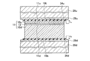
- FIG. 3 is a schematic cross-sectional view for explaining that the single crystal layer is peeled from the modified layer by bonding a metal substrate to the upper and lower surfaces of the internal modified layer forming single crystal member in the first embodiment.
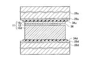
- FIG. 3 is a schematic cross-sectional view for explaining that the single crystal layer is peeled from the modified layer by bonding a metal substrate to the upper and lower surfaces of the internal modified layer forming single crystal member in the first embodiment.
- the typical perspective sectional view explaining the modification of a 1st embodiment The optical microscope photograph which shows the example of the peeling surface of a single crystal layer in 1st Embodiment.
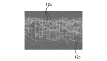
- Example 1 of Test Example 1 The optical microscope photograph of the cleaved surface of a silicon wafer in Example 1 of Test Example 1.
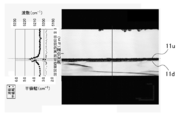
- FIG. 4 of Test example 3 the optical microscope photograph and spectrum figure of the cross section of an internal modification layer formation single crystal member.
- Example 4 of Test example 3 the optical microscope photograph and spectrum figure of the cross section of an internal modification layer formation single crystal member.
- FIG. 5 is a schematic bird's-eye view illustrating that a silicon wafer is irradiated with laser light in a comparative example of Test Example 3;
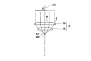
- FIG. 1 is a schematic bird's-eye view for explaining that laser light is condensed in the air by the laser condensing means in this embodiment
- FIG. 2 is a single crystal member by the laser condensing means in this embodiment. It is a typical bird's-eye view explaining that the laser beam was condensed inside.
- FIG. 3 is a schematic cross-sectional structure illustrating the single crystal substrate manufacturing method and the internal modified layer forming single crystal member 11 according to the present embodiment.
- FIG. 4 is a schematic cross-sectional view showing that a crack 12c is formed inside the single crystal member by irradiation with laser light.
- FIG. 5 is a schematic perspective sectional view showing that the modified layer 12 formed by condensing the laser beam is exposed on the side wall of the internal modified layer forming single crystal member 11.
- the single crystal substrate manufacturing method includes a step of disposing the condensing lens 15 on the single crystal member 10 as a laser condensing unit (laser condensing unit) in a non-contact manner, The step of irradiating the surface of the member 10 with the laser beam B and condensing the laser beam B inside the single crystal member 10, and the relative movement of the condenser lens 15 and the single crystal member 10, In addition, the step of forming the two-dimensional modified layer 12 and the single crystal layer 10u divided by the modified layer 12 are peeled off from the interface with the modified layer 12 so that the single layer as shown in FIG. Forming a crystal substrate 10s.
- FIG. 7 is a schematic cross-sectional view for explaining that the single crystal layer 10 u is peeled from the modified layer 12.
- the single crystal layer 10u is described as being peeled from the interface 10u with the modified layer 12.
- the present invention is not limited to peeling from the interface 10u, and the peeling is performed within the modified layer 12. It may be made to occur.
- the condensing lens 15 is configured to correct aberration due to the refractive index of the single crystal member 10. Specifically, as shown in FIG. 1, in the present embodiment, the condensing lens 15 is configured such that when the condensing lens 15 condenses in the air, the laser light that has reached the outer peripheral portion E of the condensing lens 15 is condensed. The laser beam is corrected so as to be condensed on the condensing lens side with respect to the laser light reaching the central portion M. That is, when the light is condensed, the condensing point EP of the laser light reaching the outer peripheral portion E of the condensing lens 15 is condensed compared to the condensing point MP of the laser light reaching the central portion M of the condensing lens 15. The correction is made so that the position is close to the lens 15.
- the condensing lens 15 includes a first lens 16 that condenses in the air, and a second lens 18 disposed between the first lens 16 and the single crystal member 10. .
- Both the first lens 16 and the second lens 18 are lenses capable of condensing laser light in a conical shape.
- the depth (interval) D from the surface 10t (irradiated side surface) of the single crystal member 10 on the side irradiated with the laser beam B to the modified layer 12 is mainly set to the first lens 16 and the surface 10t. It is the structure adjusted with the distance L1. Further, the thickness T of the modified layer 12 is adjusted mainly by the distance L2 between the second lens 18 and the surface 10t.
- aberration correction in the air is mainly performed by the first lens 16, and aberration correction in the single crystal member 10 is mainly performed by the second lens 18.
- the distances L1 and L2 are set.
- the first lens 16 in addition to a spherical or aspherical single lens, a combination lens can be used to correct various aberrations and ensure a working distance, and the NA is 0.3 to 0.7. It is preferable.
- the NA of the condensing lens 15 in the air defined by the light and its condensing point EP is preferably 0.3 to 0.85, and more preferably 0.5 to 0.85.
- the thickness of the modified layer 12 is not necessary, it is possible to dispose only one lens instead of the first lens 16 and the second lens 18. In that case, it is preferable to have a structure capable of correcting aberrations in the single crystal member.
- the size of the single crystal member 10 is not particularly limited, it is preferable that the surface 10t irradiated with the laser beam B is flattened in advance, for example, made of a thick silicon wafer of ⁇ 300 mm.
- the laser beam B is irradiated not on the peripheral surface of the single crystal member 10 but on the surface 10t from the irradiation device (not shown) through the condenser lens 15.
- the laser beam B is composed of, for example, a pulse laser beam having a pulse width of 1 ⁇ s or less, and a wavelength of 900 nm or more, preferably 1000 nm or more is selected.
- a YAG laser or the like is suitable. Used for.
- a laser oscillator may be disposed above the condensing lens 15 to emit light toward the condensing lens 15, or a reflecting mirror may be disposed above the condensing lens 15 to irradiate laser light toward the reflecting mirror. And you may make it the form reflected toward the condensing lens 15 with a reflective mirror.
- the laser beam B preferably has a wavelength of light transmittance of 1 to 80% when the single crystal substrate 10 is irradiated to a single crystal substrate having a thickness of 0.625 mm.
- a single crystal substrate of silicon since laser light having a wavelength of 800 nm or less has a large absorption, only the surface is processed and the internal modified layer 12 cannot be formed.
- a wavelength of 900 nm or more, preferably 1000 nm or more is selected.
- a CO 2 laser with a wavelength of 10.64 ⁇ m has a light transmittance that is too high, so that it is difficult to process a single crystal substrate. Therefore, a YAG fundamental wave laser is preferably used.
- the reason why the wavelength of the laser beam B is preferably 900 nm or more is that if the wavelength is 900 nm or more, the laser beam B is improved in the transmittance of the single crystal substrate made of silicon, and the modified layer 12 is reliably provided inside the single crystal substrate. It is because it can form. Laser light B is applied to the peripheral portion of the surface of the single crystal substrate or from the central portion of the surface of the single crystal substrate toward the peripheral portion.
- Modified layer formation process As a process of forming the modified layer 12 in the single crystal member 10 by relatively moving the condenser lens 15 and the single crystal member 10, for example, the single crystal member 10 is placed on an XY stage (not shown). The single crystal member 10 is held by a vacuum chuck or an electrostatic chuck.
- the condenser lens 15 and the single crystal member 10 are moved to the surface of the single crystal member 10 on the side where the condenser lens 15 is disposed.
- a large number of cracks 12c are formed by the laser beam B condensed inside the single crystal member 10.
- the aggregate of crack portions 12p having the cracks 12c is the modified layer 12 described above.
- the internal modified layer forming single crystal member 11 is manufactured.
- This internal modified layer forming single crystal member 11 includes a modified layer 12 formed inside the single crystal member, a single crystal layer 10u on the upper side of the modified layer 12 (that is, the irradiated side of the laser beam B), A single crystal portion 10d is provided below the material layer 12.
- the single crystal layer 10 u and the single crystal portion 10 d are formed by dividing the single crystal member 10 by the modified layer 12.
- laser beam deflecting means such as a galvanometer mirror or a polygon mirror may be used, and laser light scanning within the irradiation area of the condenser lens 15 may be used in combination.
- the laser beam B is focused on the surface 10t on the irradiated side of the single crystal member 10, that is, the surface 10t of the single crystal layer 10u. A mark indicating the region is attached, and then the single crystal member 10 is cut (cleaved) based on this mark, and the peripheral portion of the modified layer 12 is exposed and the single crystal layer 10u is peeled off as described later. May be performed.
- a large number of cracks 12c parallel to the irradiation axis BC of the laser beam B are formed as shown in FIG.
- the size, density, and the like of the crack 12c to be formed are preferably set in consideration of the material of the single crystal member 10 and the like from the viewpoint of easily peeling the single crystal layer 10u from the modified layer 12.
- the inner modified layer forming single crystal member 11 is cleaved so as to cross the region to be processed by the laser beam B, that is, the modified layer 12, and a cleavage plane (for example, 14a in FIGS. 3 and 5).
- -D may be confirmed by observing with a scanning electron microscope or a confocal microscope.
- a Y stage is fed under the same irradiation conditions to a single crystal member (for example, a silicon wafer) of the same material. It may be easily confirmed by performing linear processing inside the member at intervals of 6 to 50 ⁇ m, cleaving across the member, and observing the cleavage plane.
- the modified layer 12 and the single crystal layer 10u are separated.
- the modified layer 12 is exposed on the side wall of the internal modified layer forming single crystal member 11.
- cleavage is performed along a predetermined crystal plane of the single crystal portion 10d and the single crystal layer 10u.
- FIG. 5 a structure in which the modified layer 12 is sandwiched between the single crystal layer 10u and the single crystal portion 10d is obtained.
- the surface 10t of the single crystal layer 10u is a surface on the side irradiated with the laser beam B.
- the exposure work is omitted. It is possible.
- metal substrates 28u and 28d are bonded to the upper and lower surfaces of the internal modified layer forming single crystal member 11, respectively. That is, the metal substrate 28u is bonded to the surface 10t of the single crystal layer 10u with the adhesive 34u, and the metal substrate 28d is bonded to the surface 10b of the single crystal portion 10d with the adhesive 34d.
- Oxide layers 29u and 29d are formed on the surfaces of the metal substrates 28u and 28d, respectively.
- the oxide layer 29u is bonded to the surface 10t
- the oxide layer 29d is bonded to the surface 10b.
- a SUS peeling auxiliary plate is used as the metal substrates 28u and 28d.
- the adhesive an adhesive that is used in a normal semiconductor manufacturing process and is used as a so-called wax for fixing a commercially available silicon ingot is used.
- the adhesive bonded with this adhesive is immersed in water, the adhesive strength of the adhesive is reduced, so that the adhesive and the adherend (single crystal layer 10u) can be easily separated.
- the metal substrate 28u is attached to the surface 10t of the single crystal layer 10u with a temporary fixing adhesive, and the metal substrate 28u is lined and peeled by applying a force.
- the adhesive strength of the temporary fixing adhesive only needs to be stronger than the force necessary for peeling at the interface 11u between the modified layer 12 and the single crystal layer 10u.
- the size and density of the crack 12c to be formed may be adjusted.
- the temporary fixing adhesive for example, an adhesive made of an acrylic two-component monomer component that cures using metal ions as a reaction initiator is used.
- the uncured monomer and the cured reaction product are water-insoluble, it is possible to prevent the peeling surface 10f (for example, the peeling surface of the silicon wafer) of the single crystal layer 10u exposed when peeling in water from being contaminated. .
- the coating thickness of the temporary fixing adhesive is preferably 0.1 to 1 mm, more preferably 0.15 to 0.35 mm before curing. If the application thickness of the temporary fixing adhesive is excessively large, it takes a long time to be completely cured, and cohesive failure of the temporary fixing adhesive is likely to occur when the single crystal member (silicon wafer) is cleaved. . Moreover, when application
- the application thickness of the temporary fixing adhesive may be controlled by using a method of fixing the metal substrates 28u and 28d to be bonded to an arbitrary height, but simply using a shim plate. Can do.
- the necessary parallelism may be obtained using one or more auxiliary plates.
- the metal substrates 28u and 28d are bonded to the upper and lower surfaces of the internal modified layer-forming single crystal member 11 with a temporary fixing adhesive, they may be bonded one by one or may be bonded simultaneously on both sides.
- the metal substrate is bonded to one side and the adhesive is cured, and then the metal substrate is bonded to the other side.
- the surface to which the temporary fixing adhesive is applied may be the upper surface or the lower surface of the internal modified layer forming single crystal member 11.
- a resin film not containing metal ions may be used as the cover layer.
- machining such as a punch hole for fixing the apparatus may be performed.
- the metal substrate to be bonded undergoes a peeling process in water, it is preferable to form a passive layer for the purpose of suppressing contamination of the silicon wafer, and an oxide layer (oxide film) formed for the purpose of reducing the takt time for peeling in water. A thinner layer is preferred.
- the surface of the metal surface is easily obtained by removing the oxide layer on the metal surface by a mechanical or chemical method and providing an anchor effect.
- a mechanical or chemical method include acid cleaning using chemicals and degreasing treatment.
- Specific examples of the mechanical method include sand blasting and shot blasting.
- the method of damaging the surface of a metal substrate with sand paper is the simplest, and the particle size is preferably # 80 to 2000. Considering the surface damage of the substrate made, # 150 to 800 is more preferable.
- the method for applying the forces Fu and Fd is not particularly limited.
- the side wall of the internal modified layer forming single crystal member 11 is etched to form grooves 36 in the modified layer 12, and as shown in FIG.
- the forces Fu and Fd may be generated by press-fitting (for example, a cutter blade).
- an upward force component Fu and a downward force component Fd may be generated by applying a force F from the angular direction to the internal modified layer forming single crystal member 11.
- the peeling surface 10f of the single crystal substrate 10s obtained in this way is a rough surface as shown in FIG. 11, for example.
- FIG. 11 is an optical micrograph of the peeling surface 10f of the single crystal substrate 10s.
- a surface 10H cleaved in the crystal orientation plane is also generated in part and is shown.
- the energy of the laser beam B can be concentrated on the thin thickness portion in the single crystal member 10 with the condenser lens 15 having a large NA. Therefore, the internal modified layer forming single crystal member 11 in which the modified layer (working region) 12 having a small thickness T (length along the irradiation axis BC of the laser beam B) is formed in the single crystal member 10 is manufactured. be able to. Then, it is easy to manufacture the thin single crystal substrate 10 s by peeling the single crystal layer 10 u from the modified layer 12. Further, such a thin single crystal substrate 10s can be easily manufactured in a relatively short time. In addition, since the number of single crystal substrates 10 s can be obtained from the single crystal member 10 by suppressing the thickness of the modified layer 12, the product rate can be improved.
- the modified layer 12 an aggregate of crack portions 12p parallel to the irradiation axis BC of the laser beam B is formed. Thereby, peeling of the modified layer 12 and the single crystal layer 10 is easy.
- the peeling surface 10f is roughened by peeling from the interface 11u on the laser light irradiated side of the interfaces 11u and 11d.
- a roughened peeling surface 10f as a surface to be irradiated with sunlight, it is possible to improve the light collection efficiency when applied to a solar cell.
- the single crystal substrate 10s is obtained by bonding and peeling the metal substrate 28u having the oxide layer 29u on the surface to the surface of the single crystal layer 10u. Therefore, an adhesive used in a normal semiconductor manufacturing process can be used for bonding to a metal substrate, and a cyanoacrylate adhesive having a strong adhesive force used when bonding an acrylic plate must be used. That's it. Moreover, since the adhesive strength of the adhesive is greatly reduced by being immersed in water after peeling, the single crystal substrate 10s can be easily separated from the metal substrate 28u.
- the metal substrates 28u and 28d are respectively attached to the upper and lower surfaces of the internal modified layer forming single crystal member 11, and the metal substrates 28u and 28d are peeled by applying force to the single crystal substrate. Although it has been described by forming 10 s, it may be removed by removing the modified layer 12 by etching.
- the single crystal member 10 is not limited to a silicon wafer, but an ingot of a silicon wafer, an ingot of single crystal sapphire, SiC, or a wafer cut from the ingot, or another crystal (GaN, GaAs, InP) on this surface. Etc.) can be applied. Further, the plane orientation of the single crystal member 10 is not limited to (100), and other plane orientations can be used.
- Example 1 The inventor prepared a single-crystal silicon wafer 10 (thickness: 625 ⁇ m) that was mirror-polished as the single-crystal member 10.
- the silicon wafer 10 is placed on an XY stage, and the second plano-convex lens is used as the second lens 18 at a distance of 0.34 mm from the surface 10t on the laser beam irradiated side of the silicon wafer 10. 18 was placed.
- the second plano-convex lens 18 is a lens having a radius of curvature of 7.8 mm, a thickness of 3.8 mm, and a refractive index of 1.58.
- a first plano-convex lens 16 having an NA of 0.55 is disposed as the first lens 16.
- the modified layer 12 is formed inside the silicon wafer 10 by irradiating the laser beam B having a wavelength of 1064 nm, a repetition frequency of 100 kHz, a pulse width of 60 seconds, and an output of 1 W, and passing through the first plano-convex lens 16 and the second plano-convex lens 18. did.
- the depth D from the silicon wafer surface 10t to the processing region, that is, the depth D to the modified layer 12 was controlled by adjusting the mutual position of the first plano-convex lens 16 and the silicon wafer surface 10t.
- the thickness T of the modified layer 12 was controlled by adjusting the mutual position of the second plano-convex lens 18 and the silicon wafer surface 10t.
- the laser beam B is irradiated while being moved at a constant speed of 15 mm on the X stage, then sent 1 ⁇ m on the Y stage, and this is repeated to repeat the laser beam in an area of 15 mm ⁇ 15 mm.
- the modified layer 12 was formed by performing internal irradiation. As a result, the internal modified layer forming single crystal member 11 having the single crystal layer 10u on the upper side of the modified layer 12 (that is, the irradiated side of the laser beam B) and the single crystal part 10d on the lower side of the modified layer 12 is obtained.
- the single crystal layer 10 u and the single crystal portion 10 d are formed by dividing the silicon wafer 10 by the modified layer 12.
- the silicon wafer 10 was cleaved so as to cross the modified layer 12, and the cleaved surface was observed with an optical microscope (scanning electron microscope). An optical micrograph of the cleaved surface observed is shown in FIG. It was confirmed that clear cracks 12c were formed at intervals of 1 ⁇ m.
- the modified layer 12 was formed by changing the above-described implementation conditions only by sending the Y stage at 10 ⁇ m instead of 1 ⁇ m.
- the silicon wafer 10 was cleaved so as to cross the modified layer 12, and the cleaved surface was observed with an optical microscope (scanning electron microscope). An optical micrograph of the observed cleavage plane is shown in FIG. It was confirmed that clear cracks 12c were formed at intervals of 10 ⁇ m.
- Example 3 after irradiating the laser beam as in Example 2, the laser beam was repeatedly irradiated while being moved at a constant speed on the Y stage after being fed by 10 ⁇ m on the X stage. That is, the laser beam was irradiated in a lattice shape. Similarly, the silicon wafer 10 was cleaved so as to cross the modified layer 12, and the cleaved surface was observed with an optical microscope (scanning electron microscope). The cracks were formed more clearly than in Example 2.
- Example 2 ⁇ Test Example 2>
- the inventor uses the same silicon wafer as the silicon wafer 10 used in Test Example 1 and forms the internal modified layer-forming single crystal member 11 formed by forming the modified layer 12 under the conditions of Example 1.
- the single crystal layer 10u was peeled off using the metal substrates 28u and 28d to obtain a single crystal substrate 10s.
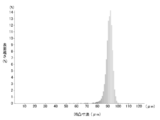
- the peeling surface 10f of the single crystal substrate 10s was observed with a laser confocal microscope, the measurement diagram shown in FIG. 14 was obtained, and it was confirmed that irregularities having a particle size of 50 to 100 ⁇ m were formed on the peeling surface 10f.
- the horizontal axis is the unevenness dimension ( ⁇ m display), and the vertical axis is the surface roughness (% display).
- Example 4 The present inventor prepared a single crystal silicon wafer 10 (thickness: 625 ⁇ m) having a mirror polished surface on both sides as the single crystal member 10. As Example 4, this silicon wafer 10 was placed on an XY stage and irradiated with a pulsed laser beam having a wavelength of 1064 nm to form a modified layer 12 having a square shape in a plan view with a side of 5 mm. The silicon wafer (internally modified layer-forming single crystal member) was cleaved to expose the cross section of the modified layer 12, and this cross section was observed with a scanning electron microscope. The thickness T of the modified layer 12 was 30 ⁇ m.
- FIG. 16 is a schematic bird's-eye view illustrating that the laser beam is collected in the air by the laser focusing unit in this comparative example.
- a condensing lens 115 is disposed instead of the condensing lens 15 as a laser condensing unit as compared with the fourth embodiment.
- the condensing lens 115 used in this comparative example includes a first lens 116 that is a plano-convex lens, and an aberration-enhancing glass plate 118 that is disposed between the first lens 116 and the surface of the silicon wafer 100.
- the laser beam B that forms the laser spot SP on the surface of the silicon wafer 100 that is the object to be irradiated is refracted by the silicon wafer surface 100t and is used as the laser beam.
- an image having a predetermined depth position and width is formed. That is, the modified layer 112 (processed region) can be formed in the silicon wafer with a predetermined thickness V at a predetermined depth position.
- the predetermined thickness V is larger than the thickness T of the modified layer 12 of the fourth embodiment.
- a cover glass having a diameter of 0.15 mm was attached as an aberration-enhancing glass plate 118 to a microscope objective lens having an NA of 0.8 and a magnification of 100 times.
- a pulsed laser having a wavelength of 1064 nm was irradiated onto the silicon wafer 100 with the same frequency and output as in the case of Example 4 to form a modified layer 112 having a square shape in plan view with a side of 5 mm.
- the silicon wafer 100 was cleaved to expose a cross section of the modified layer 112, and this cross section was observed with a scanning electron microscope.
- the thickness of the modified layer 112 was 80 to 100 ⁇ m.
- Example 4 compared with the comparative example, the thickness of the modified layer 112 processed and formed with the laser beam inside the silicon wafer (inside the single crystal member) is small, so that energy loss due to processing is reduced. It was found that it can be reduced.
- Example 4 a large compressive stress exists in the vicinity of the interfaces 11u and 11d. Even in the presence of this stress, the single crystal layer is more easily separated from the modified layer in Example 4 than in the comparative example.
- FIG. 17 is a schematic bird's-eye view of the single-crystal member internal processing apparatus used for explaining the single-crystal substrate manufacturing method and the internal modified layer-forming single crystal member according to this embodiment.
- the single crystal member internal processing apparatus 69 used in this embodiment includes a rotary stage 70 that holds the single crystal member 10 placed on the upper surface side, and a rotary stage control means 72 that controls the number of rotations of the rotary stage 70. Substrate rotating means 74 is provided.
- the single crystal member internal processing device 69 includes a laser light source 76, a condensing lens 15, and a focal position adjusting tool (not shown) that adjusts the distance from the condensing lens 15 to the rotary stage 70. 80.
- the single crystal member internal processing device 69 includes an X-direction moving stage 84 that relatively moves the rotary stage 70 and the condenser lens 15 between the rotary shaft 70 c of the rotary stage 70 and the outer periphery of the rotary stage 70.
- a Y-direction moving stage 86 is provided.
- the single crystal member internal processing apparatus 69 is used to place the single crystal member 10 on the rotary stage 70, and while rotating the single crystal member 10 at a constant speed on the rotary stage 70, Similarly, the laser beam B is irradiated, and then the rotary stage 70 is moved by the X direction moving stage 84 and the Y direction moving stage 86, and the irradiation position of the laser light B is set at a predetermined interval (1 ⁇ m,
- the two-dimensional modified layer can be formed inside the single crystal member 10 by repeating irradiation after being sent at 5 ⁇ m, 10 ⁇ m, etc.
- a plurality of square-shaped single crystal members may be arranged on the rotary stage 70 symmetrically with respect to the rotary shaft 70c with an interval.
- the crack by condensing of the laser beam B can be arrange
- the thinly cut single crystal substrate can be applied to a solar cell as long as it is a Si substrate, and a sapphire substrate such as a GaN-based semiconductor device.
- a solar cell as long as it is a Si substrate, and a sapphire substrate such as a GaN-based semiconductor device.
Landscapes
- Chemical & Material Sciences (AREA)
- Engineering & Computer Science (AREA)
- Optics & Photonics (AREA)
- Physics & Mathematics (AREA)
- Organic Chemistry (AREA)
- Crystallography & Structural Chemistry (AREA)
- Materials Engineering (AREA)
- Metallurgy (AREA)
- Mechanical Engineering (AREA)
- Plasma & Fusion (AREA)
- Inorganic Chemistry (AREA)
- Mechanical Treatment Of Semiconductor (AREA)
- Laser Beam Processing (AREA)
- Processing Of Stones Or Stones Resemblance Materials (AREA)
Abstract
Description
まず、第1実施形態について説明する。図1は、本実施形態で、レーザ集光手段により空気中でレーザ光を集光したことを説明する模式的鳥瞰図であり、図2は、本実施形態で、レーザ集光手段により単結晶部材内部にレーザ光を集光したことを説明する模式的鳥瞰図である。図3は、本実施形態に係る単結晶基板製造方法および内部改質層形成単結晶部材11を説明する模式的断面構造である。図4は、レーザ光の照射により単結晶部材内部にクラック12cが形成されていることを示す模式的断面図である。図5は、内部改質層形成単結晶部材11の側壁に、レーザ光の集光によって形成された改質層12を露出させたことを示す模式的斜視断面図である。
集光レンズ15と単結晶部材10とを相対的に移動させて単結晶部材10内部に改質層12を形成する工程としては、例えば、単結晶部材10をXYステージ(図示せず)上に載置し、真空チャック、静電チャックなどでこの単結晶部材10を保持する。
この後、改質層12と単結晶層10uとの剥離を行う。本実施形態では、まず、内部改質層形成単結晶部材11の側壁に改質層12を露出させる。露出させるには、例えば、単結晶部10d、単結晶層10uの所定の結晶面に沿ってへき開する。この結果、図5に示すように、単結晶層10uと単結晶部10dとによって改質層12が挟まれた構造のものが得られる。なお、単結晶層10uの表面10tはレーザ光Bの被照射側の面である。
本発明者は、単結晶部材10として鏡面研磨した単結晶のシリコンウェハ10(厚み625μm)を準備した。そして、実施例1として、このシリコンウェハ10をXYステージに載置し、シリコンウェハ10のレーザ光の被照射側の表面10tからの0.34mmの距離に、第2レンズ18として第2平凸レンズ18を配置した。この第2平凸レンズ18は、曲率半径7.8mm、厚み3.8mm、屈折率1.58のレンズである。また、第1レンズ16としてNAが0.55の第1平凸レンズ16を配置した。
また、本発明者は、試験例1で用いたシリコンウェハ10と同様のシリコンウェハを用い、実施例1の実施条件で改質層12を形成してなる内部改質層形成単結晶部材11を製造した。そして、金属製基板28u、28dを用いて単結晶層10uを剥離し、単結晶基板10sを得た。この単結晶基板10sの剥離面10fをレーザ共焦点顕微鏡で観察したところ、図14に示す計測図が得られ、粒径50~100μmの凹凸が剥離面10fに形成されていることが確認された。ここで、図14では、横軸が凹凸寸法(μm表示)であり、縦軸が表面粗さ(%表示)である。
(実施例4)
本発明者は、単結晶部材10として両面を鏡面研磨した単結晶のシリコンウェハ10(厚み625μm)を準備した。そして、実施例4として、このシリコンウェハ10をXYステージに載置し、波長1064nmのパルスレーザ光を照射し、一辺が5mmの平面視正方形状の改質層12を形成した。そして、このシリコンウェハ(内部改質層形成単結晶部材)をへき開することで改質層12の断面を露出させ、この断面を走査型電子顕微鏡で観察した。改質層12の厚みTは30μmであった。
また、本発明者は、実施例4で用いたシリコンウェハと同様のシリコンウェハを用い、以下のようにして比較例の試験を行った。図16は、本比較例で、レーザ集光手段により空気中でレーザ光を集光したことを説明する模式的鳥瞰図である。比較例では、実施例4に比べ、レーザ集光手段として、集光レンズ15に代えて集光レンズ115が配置されている。本比較例で用いるこの集光レンズ115は、平凸レンズである第1レンズ116と、第1レンズ116とシリコンウェハ100表面との間に配置された収差増強用のガラス板118と、で構成される。この収差増強用のガラス板118をこのように配置することによって、被照射体であるシリコンウェハ100の表面にレーザスポットSPを形成するレーザ光Bは、シリコンウェハ表面100tで屈折されてレーザ光としてシリコンウェハ内部に進入し、シリコンウェハ内部に集光点を結ぶ際に、所定の深さ位置および幅を有する像を結ぶことになる。すなわち、シリコンウェハ内部に改質層112(加工領域)を所定の深さ位置に所定の厚みVで形成することができる。ここで収差増強用のガラス板118によって収差が増強されているので、この所定の厚みVは、実施例4の改質層12の厚みTよりも大きくなる。
次に、第2実施形態について説明する。図17は、本実施形態に係る単結晶基板製造方法および内部改質層形成単結晶部材を説明する上で用いる単結晶部材内部加工装置の模式的鳥瞰図である。
10u 単結晶層
10d 単結晶部
10s 単結晶基板
10t 表面
10b 表面
10f 剥離面
11 内部改質層形成単結晶部材
11u 界面
12 改質層
12p クラック部
15 集光レンズ(レーザ集光手段)
28u 金属製基板
29u 酸化層
B レーザ光
BC 照射軸
E 外周部
M 中央部
L1 距離
L2 距離
T 厚み
Claims (10)
- レーザ光を出射するとともに単結晶部材の屈折率に起因する収差を補正するレーザ集光手段を、前記単結晶部材上に非接触に配置する工程と、
前記レーザ集光手段により、前記単結晶部材表面にレーザ光を照射して前記単結晶部材内部に前記レーザ光を集光する工程と、
前記レーザ集光手段と前記単結晶部材とを相対的に移動させて、前記単結晶部材内部に、2次元状の改質層を形成する工程と、
前記改質層により分断されてなる単結晶層を前記改質層から剥離することで単結晶基板を形成する工程と
を有することを特徴とする単結晶基板の製造方法。 - 前記改質層として、前記レーザ光の照射軸と平行なクラック部の集合体を形成することを特徴とする請求項1に記載の単結晶基板の製造方法。
- 前記剥離によって形成された剥離面が粗面であることを特徴とする請求項2に記載の単結晶基板の製造方法。
- 前記単結晶基板を形成する工程では、前記改質層の両面側のうち前記レーザ光を照射する側の界面から剥離することを特徴とする請求項1に記載の単結晶基板の製造方法。
- 前記単結晶基板を形成する工程では、表面に酸化層を有する金属製基板を前記単結晶層の表面に接着して剥離することを特徴とする請求項1に記載の単結晶基板の製造方法。
- 前記レーザ集光手段は、空気中で集光した際に、前記レーザ集光手段の外周部に到達した光線が前記レーザ集光手段の中央部に到達した光線よりも前記レーザ集光手段側で集光するように補正することを特徴とする請求項1に記載の単結晶基板の製造方法。
- 前記レーザ集光手段は、
空気中で集光する第1のレンズと、
前記第1のレンズと前記単結晶部材との間に配置される第2のレンズと、
を含むことを特徴とする請求項6に記載の単結晶基板の製造方法。 - レーザ光が照射される側の前記単結晶部材表面から前記改質層までの距離を、前記第1のレンズと該単結晶部材表面との距離で調整することを特徴とする請求項7に記載の単結晶基板の製造方法。
- 前記改質層の厚みを、レーザ光が照射される側の前記単結晶部材表面と前記第2のレンズとの距離で調整することを特徴とする請求項8に記載の単結晶基板の製造方法。
- 単結晶部材に表面からレーザ光を照射して内部で集光することで前記単結晶部材の内部に改質層を形成し、前記改質層から単結晶基板を剥離するための内部改質層形成単結晶部材の製造方法であって、
レーザ光を出射するとともに単結晶部材の屈折率に起因する収差を補正するレーザ集光手段とを、前記単結晶部材上に非接触に配置する工程と、
前記レーザ集光手段により、前記単結晶部材表面にレーザ光を照射して前記単結晶部材内部に前記レーザ光を集光する工程と、
前記レーザ集光手段と前記単結晶部材とを相対的に移動させて、前記単結晶部材内部に、2次元状の改質層を形成する工程と
を有することを特徴とする、内部改質層形成単結晶部材の製造方法。
Priority Applications (4)
| Application Number | Priority Date | Filing Date | Title |
|---|---|---|---|
| KR1020137021347A KR20130103623A (ko) | 2011-02-10 | 2011-02-10 | 단결정 기판의 제조 방법 및 내부 개질층 형성 단결정 부재의 제조 방법 |
| US13/984,047 US20130312460A1 (en) | 2011-02-10 | 2011-02-10 | Manufacturing method of single crystal substrate and manufacturing method of internal modified layer-forming single crystal member |
| JP2012556740A JP5875121B2 (ja) | 2011-02-10 | 2011-02-10 | 単結晶基板の製造方法および内部改質層形成単結晶部材の製造方法 |
| PCT/JP2011/052949 WO2012108054A1 (ja) | 2011-02-10 | 2011-02-10 | 単結晶基板の製造方法および内部改質層形成単結晶部材の製造方法 |
Applications Claiming Priority (1)
| Application Number | Priority Date | Filing Date | Title |
|---|---|---|---|
| PCT/JP2011/052949 WO2012108054A1 (ja) | 2011-02-10 | 2011-02-10 | 単結晶基板の製造方法および内部改質層形成単結晶部材の製造方法 |
Publications (1)
| Publication Number | Publication Date |
|---|---|
| WO2012108054A1 true WO2012108054A1 (ja) | 2012-08-16 |
Family
ID=46638292
Family Applications (1)
| Application Number | Title | Priority Date | Filing Date |
|---|---|---|---|
| PCT/JP2011/052949 Ceased WO2012108054A1 (ja) | 2011-02-10 | 2011-02-10 | 単結晶基板の製造方法および内部改質層形成単結晶部材の製造方法 |
Country Status (4)
| Country | Link |
|---|---|
| US (1) | US20130312460A1 (ja) |
| JP (1) | JP5875121B2 (ja) |
| KR (1) | KR20130103623A (ja) |
| WO (1) | WO2012108054A1 (ja) |
Cited By (12)
| Publication number | Priority date | Publication date | Assignee | Title |
|---|---|---|---|---|
| JP2016111147A (ja) * | 2014-12-04 | 2016-06-20 | 株式会社ディスコ | ウエーハの生成方法 |
| JP2016111146A (ja) * | 2014-12-04 | 2016-06-20 | 株式会社ディスコ | ウエーハの生成方法 |
| JP2016111145A (ja) * | 2014-12-04 | 2016-06-20 | 株式会社ディスコ | ウエーハの生成方法 |
| JP2017123405A (ja) * | 2016-01-07 | 2017-07-13 | 株式会社ディスコ | SiCウエーハの生成方法 |
| CN107053498A (zh) * | 2015-09-15 | 2017-08-18 | 株式会社迪思科 | 氮化镓基板的生成方法 |
| JP2017177214A (ja) * | 2016-03-29 | 2017-10-05 | 国立大学法人埼玉大学 | 基板加工方法および基板加工装置 |
| JP2017216266A (ja) * | 2016-05-30 | 2017-12-07 | 株式会社ディスコ | レーザー加工装置、およびウエーハの生成方法 |
| JP2017213603A (ja) * | 2013-08-02 | 2017-12-07 | ロフィン−ジナール テクノロジーズ インコーポレイテッド | 透明材料の内部でレーザーフィラメンテーションを実行するシステム |
| JP2018027565A (ja) * | 2016-08-16 | 2018-02-22 | 国立大学法人埼玉大学 | 基板加工方法および基板加工装置 |
| JP2018043340A (ja) * | 2016-09-15 | 2018-03-22 | 株式会社荏原製作所 | 基板加工方法および基板加工装置 |
| CN120193333A (zh) * | 2025-05-22 | 2025-06-24 | 浙江晶盛机电股份有限公司 | 碳化硅衬底及碳化硅衬底制备方法 |
| EP4530010A3 (de) * | 2014-11-27 | 2025-06-25 | Siltectra GmbH | Festkörperteilung mittels stoffumwandlung |
Families Citing this family (53)
| Publication number | Priority date | Publication date | Assignee | Title |
|---|---|---|---|---|
| WO2014079478A1 (en) | 2012-11-20 | 2014-05-30 | Light In Light Srl | High speed laser processing of transparent materials |
| EP2754524B1 (de) | 2013-01-15 | 2015-11-25 | Corning Laser Technologies GmbH | Verfahren und Vorrichtung zum laserbasierten Bearbeiten von flächigen Substraten, d.h. Wafer oder Glaselement, unter Verwendung einer Laserstrahlbrennlinie |
| EP2781296B1 (de) | 2013-03-21 | 2020-10-21 | Corning Laser Technologies GmbH | Vorrichtung und verfahren zum ausschneiden von konturen aus flächigen substraten mittels laser |
| ITAN20130232A1 (it) * | 2013-12-05 | 2015-06-06 | Munoz David Callejo | Metodo per ottenere una pluralita' di lamine da un lingotto di materiale con struttura monocristallina |
| ITAN20130231A1 (it) * | 2013-12-05 | 2015-06-06 | Munoz David Callejo | Procedimento per ottenere una pluralita' di lamine da un lingotto di materiale con struttura monocristallina |
| KR20160093593A (ko) * | 2013-12-05 | 2016-08-08 | 일렉트로 싸이언티픽 인더스트리이즈 인코포레이티드 | 거친 표면을 가진 기판을 내부적으로 마킹하는 방법 및 장치 |
| US9701563B2 (en) | 2013-12-17 | 2017-07-11 | Corning Incorporated | Laser cut composite glass article and method of cutting |
| US9850160B2 (en) | 2013-12-17 | 2017-12-26 | Corning Incorporated | Laser cutting of display glass compositions |
| US9676167B2 (en) | 2013-12-17 | 2017-06-13 | Corning Incorporated | Laser processing of sapphire substrate and related applications |
| US10442719B2 (en) | 2013-12-17 | 2019-10-15 | Corning Incorporated | Edge chamfering methods |
| US11556039B2 (en) | 2013-12-17 | 2023-01-17 | Corning Incorporated | Electrochromic coated glass articles and methods for laser processing the same |
| US10293436B2 (en) | 2013-12-17 | 2019-05-21 | Corning Incorporated | Method for rapid laser drilling of holes in glass and products made therefrom |
| US9815730B2 (en) | 2013-12-17 | 2017-11-14 | Corning Incorporated | Processing 3D shaped transparent brittle substrate |
| US20150165560A1 (en) | 2013-12-17 | 2015-06-18 | Corning Incorporated | Laser processing of slots and holes |
| DE102015000449A1 (de) * | 2015-01-15 | 2016-07-21 | Siltectra Gmbh | Festkörperteilung mittels Stoffumwandlung |
| TWI730945B (zh) | 2014-07-08 | 2021-06-21 | 美商康寧公司 | 用於雷射處理材料的方法與設備 |
| EP3169479B1 (en) | 2014-07-14 | 2019-10-02 | Corning Incorporated | Method of and system for arresting incident crack propagation in a transparent material |
| CN107073641B (zh) | 2014-07-14 | 2020-11-10 | 康宁股份有限公司 | 接口块;用于使用这种接口块切割在波长范围内透明的衬底的系统和方法 |
| KR20170028943A (ko) * | 2014-07-14 | 2017-03-14 | 코닝 인코포레이티드 | 조정가능한 레이저 빔 촛점 라인을 사용하여 투명한 재료를 처리하는 방법 및 시스템 |
| WO2016010949A1 (en) | 2014-07-14 | 2016-01-21 | Corning Incorporated | Method and system for forming perforations |
| TWI610411B (zh) * | 2014-08-14 | 2018-01-01 | 艾馬克科技公司 | 用於半導體晶粒互連的雷射輔助接合 |
| CN107000125B (zh) * | 2014-11-27 | 2022-08-12 | 西尔特克特拉有限责任公司 | 基于激光器的分离方法 |
| US10047001B2 (en) | 2014-12-04 | 2018-08-14 | Corning Incorporated | Glass cutting systems and methods using non-diffracting laser beams |
| CN107406293A (zh) | 2015-01-12 | 2017-11-28 | 康宁股份有限公司 | 使用多光子吸收方法来对经热回火的基板进行激光切割 |
| DE102015000451A1 (de) * | 2015-01-15 | 2016-07-21 | Siltectra Gmbh | Unebener Wafer und Verfahren zum Herstellen eines unebenen Wafers |
| US11773004B2 (en) | 2015-03-24 | 2023-10-03 | Corning Incorporated | Laser cutting and processing of display glass compositions |
| KR20170131638A (ko) | 2015-03-27 | 2017-11-29 | 코닝 인코포레이티드 | 가스 투과성 유리창 및 이의 제작방법 |
| JP6494382B2 (ja) * | 2015-04-06 | 2019-04-03 | 株式会社ディスコ | ウエーハの生成方法 |
| WO2017011296A1 (en) | 2015-07-10 | 2017-01-19 | Corning Incorporated | Methods of continuous fabrication of holes in flexible substrate sheets and products relating to the same |
| JP6482423B2 (ja) * | 2015-07-16 | 2019-03-13 | 株式会社ディスコ | ウエーハの生成方法 |
| JP6472347B2 (ja) * | 2015-07-21 | 2019-02-20 | 株式会社ディスコ | ウエーハの薄化方法 |
| JP6486239B2 (ja) | 2015-08-18 | 2019-03-20 | 株式会社ディスコ | ウエーハの加工方法 |
| JP6938543B2 (ja) | 2016-05-06 | 2021-09-22 | コーニング インコーポレイテッド | 透明基板からの、輪郭設定された形状のレーザ切断及び取り外し |
| US10410883B2 (en) | 2016-06-01 | 2019-09-10 | Corning Incorporated | Articles and methods of forming vias in substrates |
| JP6669594B2 (ja) * | 2016-06-02 | 2020-03-18 | 株式会社ディスコ | ウエーハ生成方法 |
| US10794679B2 (en) | 2016-06-29 | 2020-10-06 | Corning Incorporated | Method and system for measuring geometric parameters of through holes |
| KR20190035805A (ko) | 2016-07-29 | 2019-04-03 | 코닝 인코포레이티드 | 레이저 처리를 위한 장치 및 방법 |
| KR102423775B1 (ko) | 2016-08-30 | 2022-07-22 | 코닝 인코포레이티드 | 투명 재료의 레이저 가공 |
| US10730783B2 (en) | 2016-09-30 | 2020-08-04 | Corning Incorporated | Apparatuses and methods for laser processing transparent workpieces using non-axisymmetric beam spots |
| KR102428350B1 (ko) | 2016-10-24 | 2022-08-02 | 코닝 인코포레이티드 | 시트형 유리 기판의 레이저 기반 기계 가공을 위한 기판 프로세싱 스테이션 |
| US10752534B2 (en) | 2016-11-01 | 2020-08-25 | Corning Incorporated | Apparatuses and methods for laser processing laminate workpiece stacks |
| JP6781639B2 (ja) * | 2017-01-31 | 2020-11-04 | 株式会社ディスコ | ウエーハ生成方法 |
| US10688599B2 (en) | 2017-02-09 | 2020-06-23 | Corning Incorporated | Apparatus and methods for laser processing transparent workpieces using phase shifted focal lines |
| JP6795811B2 (ja) * | 2017-02-16 | 2020-12-02 | 国立大学法人埼玉大学 | 剥離基板製造方法 |
| US10580725B2 (en) | 2017-05-25 | 2020-03-03 | Corning Incorporated | Articles having vias with geometry attributes and methods for fabricating the same |
| US11078112B2 (en) | 2017-05-25 | 2021-08-03 | Corning Incorporated | Silica-containing substrates with vias having an axially variable sidewall taper and methods for forming the same |
| US10626040B2 (en) | 2017-06-15 | 2020-04-21 | Corning Incorporated | Articles capable of individual singulation |
| US12180108B2 (en) | 2017-12-19 | 2024-12-31 | Corning Incorporated | Methods for etching vias in glass-based articles employing positive charge organic molecules |
| US11554984B2 (en) | 2018-02-22 | 2023-01-17 | Corning Incorporated | Alkali-free borosilicate glasses with low post-HF etch roughness |
| WO2020129732A1 (ja) * | 2018-12-21 | 2020-06-25 | 東京エレクトロン株式会社 | 基板処理装置及び基板処理方法 |
| KR102797419B1 (ko) * | 2019-11-25 | 2025-04-21 | 삼성전자주식회사 | 기판 다이싱 방법, 반도체 소자의 제조 방법 및 그들에 의해 제조되는 반도체 칩 |
| CN112820796A (zh) * | 2020-12-31 | 2021-05-18 | 苏州索雷特自动化科技有限公司 | 一种太阳能电池制备方法及太阳能电池片 |
| KR102923408B1 (ko) * | 2024-03-12 | 2026-02-05 | 웨이브로드 주식회사 | 핫 셀프스플릿 공정을 통한 에피택셜 질화알루미늄 체적 탄성파 필터 소자용 웨이퍼, 그 제조 방법 및 체적 탄성파 필터 소자 |
Citations (5)
| Publication number | Priority date | Publication date | Assignee | Title |
|---|---|---|---|---|
| JPH09331077A (ja) * | 1996-06-10 | 1997-12-22 | Ion Kogaku Kenkyusho:Kk | 太陽電池およびその製造方法 |
| JP2005294325A (ja) * | 2004-03-31 | 2005-10-20 | Sharp Corp | 基板製造方法及び基板製造装置 |
| JP2006192503A (ja) * | 2005-01-12 | 2006-07-27 | L'air Liquide Sa Pour L'etude & L'exploitation Des Procede S Georges Claude | 二重焦点レンズを用いる、薄い金属被加工物のレーザー切断 |
| JP2010284712A (ja) * | 2009-06-15 | 2010-12-24 | Hamamatsu Photonics Kk | レーザ加工装置 |
| JP2011003624A (ja) * | 2009-06-17 | 2011-01-06 | Shin Etsu Polymer Co Ltd | 半導体ウェーハの製造方法及びその装置 |
Family Cites Families (4)
| Publication number | Priority date | Publication date | Assignee | Title |
|---|---|---|---|---|
| JP4749799B2 (ja) * | 2005-08-12 | 2011-08-17 | 浜松ホトニクス株式会社 | レーザ加工方法 |
| JP4752488B2 (ja) * | 2005-12-20 | 2011-08-17 | セイコーエプソン株式会社 | レーザ内部スクライブ方法 |
| WO2007087354A2 (en) * | 2006-01-24 | 2007-08-02 | Baer Stephen C | Cleaving wafers from silicon crystals |
| SG171947A1 (en) * | 2008-12-05 | 2011-07-28 | Agency Science Tech & Res | A wafer cutting method and a system thereof |
-
2011
- 2011-02-10 US US13/984,047 patent/US20130312460A1/en not_active Abandoned
- 2011-02-10 KR KR1020137021347A patent/KR20130103623A/ko not_active Ceased
- 2011-02-10 JP JP2012556740A patent/JP5875121B2/ja not_active Expired - Fee Related
- 2011-02-10 WO PCT/JP2011/052949 patent/WO2012108054A1/ja not_active Ceased
Patent Citations (5)
| Publication number | Priority date | Publication date | Assignee | Title |
|---|---|---|---|---|
| JPH09331077A (ja) * | 1996-06-10 | 1997-12-22 | Ion Kogaku Kenkyusho:Kk | 太陽電池およびその製造方法 |
| JP2005294325A (ja) * | 2004-03-31 | 2005-10-20 | Sharp Corp | 基板製造方法及び基板製造装置 |
| JP2006192503A (ja) * | 2005-01-12 | 2006-07-27 | L'air Liquide Sa Pour L'etude & L'exploitation Des Procede S Georges Claude | 二重焦点レンズを用いる、薄い金属被加工物のレーザー切断 |
| JP2010284712A (ja) * | 2009-06-15 | 2010-12-24 | Hamamatsu Photonics Kk | レーザ加工装置 |
| JP2011003624A (ja) * | 2009-06-17 | 2011-01-06 | Shin Etsu Polymer Co Ltd | 半導体ウェーハの製造方法及びその装置 |
Cited By (15)
| Publication number | Priority date | Publication date | Assignee | Title |
|---|---|---|---|---|
| TWI653115B (zh) | 2013-08-02 | 2019-03-11 | 柔芬新拿科技公司 | 於透明材料內部施行雷射絲化之方法 |
| JP2017213603A (ja) * | 2013-08-02 | 2017-12-07 | ロフィン−ジナール テクノロジーズ インコーポレイテッド | 透明材料の内部でレーザーフィラメンテーションを実行するシステム |
| JP2017221977A (ja) * | 2013-08-02 | 2017-12-21 | ロフィン−ジナール テクノロジーズ インコーポレイテッド | 透明材料の内部でレーザーフィラメンテーションを実行する方法および装置 |
| EP4530010A3 (de) * | 2014-11-27 | 2025-06-25 | Siltectra GmbH | Festkörperteilung mittels stoffumwandlung |
| JP2016111146A (ja) * | 2014-12-04 | 2016-06-20 | 株式会社ディスコ | ウエーハの生成方法 |
| JP2016111145A (ja) * | 2014-12-04 | 2016-06-20 | 株式会社ディスコ | ウエーハの生成方法 |
| JP2016111147A (ja) * | 2014-12-04 | 2016-06-20 | 株式会社ディスコ | ウエーハの生成方法 |
| CN107053498A (zh) * | 2015-09-15 | 2017-08-18 | 株式会社迪思科 | 氮化镓基板的生成方法 |
| JP2017123405A (ja) * | 2016-01-07 | 2017-07-13 | 株式会社ディスコ | SiCウエーハの生成方法 |
| JP2017177214A (ja) * | 2016-03-29 | 2017-10-05 | 国立大学法人埼玉大学 | 基板加工方法および基板加工装置 |
| JP2017216266A (ja) * | 2016-05-30 | 2017-12-07 | 株式会社ディスコ | レーザー加工装置、およびウエーハの生成方法 |
| TWI705868B (zh) * | 2016-05-30 | 2020-10-01 | 日商迪思科股份有限公司 | 晶圓的產生方法 |
| JP2018027565A (ja) * | 2016-08-16 | 2018-02-22 | 国立大学法人埼玉大学 | 基板加工方法および基板加工装置 |
| JP2018043340A (ja) * | 2016-09-15 | 2018-03-22 | 株式会社荏原製作所 | 基板加工方法および基板加工装置 |
| CN120193333A (zh) * | 2025-05-22 | 2025-06-24 | 浙江晶盛机电股份有限公司 | 碳化硅衬底及碳化硅衬底制备方法 |
Also Published As
| Publication number | Publication date |
|---|---|
| JPWO2012108054A1 (ja) | 2014-07-03 |
| US20130312460A1 (en) | 2013-11-28 |
| JP5875121B2 (ja) | 2016-03-02 |
| KR20130103623A (ko) | 2013-09-23 |
Similar Documents
| Publication | Publication Date | Title |
|---|---|---|
| JP5875121B2 (ja) | 単結晶基板の製造方法および内部改質層形成単結晶部材の製造方法 | |
| JP6004338B2 (ja) | 単結晶基板製造方法および内部改質層形成単結晶部材 | |
| JP5875122B2 (ja) | 単結晶基板製造方法および内部改質層形成単結晶部材 | |
| JP5843393B2 (ja) | 単結晶基板の製造方法、単結晶基板、および、内部改質層形成単結晶部材の製造方法 | |
| JP6004339B2 (ja) | 内部応力層形成単結晶部材および単結晶基板製造方法 | |
| JP6202696B2 (ja) | 単結晶基板製造方法 | |
| JP5509448B2 (ja) | 基板スライス方法 | |
| KR101802527B1 (ko) | 가공 대상물 절단 방법 | |
| KR101721709B1 (ko) | 가공 대상물 절단 방법 | |
| JP6032789B2 (ja) | 単結晶加工部材の製造方法、および、単結晶基板の製造方法 | |
| JP2014019120A (ja) | 内部加工層形成単結晶部材の製造方法 | |
| JP6531885B2 (ja) | 内部加工層形成単結晶部材およびその製造方法 | |
| WO2013115353A1 (ja) | 基板及び基板加工方法 | |
| JP5946112B2 (ja) | 基板加工方法 | |
| JP2015119076A (ja) | 内部加工層形成単結晶部材およびその製造方法 | |
| JP2005277136A (ja) | 基板製造方法および基板製造装置 | |
| JP2015123465A (ja) | 基板加工装置及び基板加工方法 | |
| JP5950269B2 (ja) | 基板加工方法及び基板 | |
| JP6202695B2 (ja) | 単結晶基板製造方法 | |
| US10373855B2 (en) | Method for processing a wafer and method for processing a carrier | |
| JP2019140411A (ja) | 内部加工層形成単結晶部材の製造方法 | |
| JP2019069870A (ja) | 基板製造方法 | |
| JP6265522B2 (ja) | 表面3次元構造部材の製造方法 | |
| JP2019140410A (ja) | 内部加工層形成単結晶部材およびその製造方法 |
Legal Events
| Date | Code | Title | Description |
|---|---|---|---|
| 121 | Ep: the epo has been informed by wipo that ep was designated in this application |
Ref document number: 11858323 Country of ref document: EP Kind code of ref document: A1 |
|
| ENP | Entry into the national phase |
Ref document number: 2012556740 Country of ref document: JP Kind code of ref document: A |
|
| WWE | Wipo information: entry into national phase |
Ref document number: 13984047 Country of ref document: US |
|
| NENP | Non-entry into the national phase |
Ref country code: DE |
|
| ENP | Entry into the national phase |
Ref document number: 20137021347 Country of ref document: KR Kind code of ref document: A |
|
| 122 | Ep: pct application non-entry in european phase |
Ref document number: 11858323 Country of ref document: EP Kind code of ref document: A1 |