WO2012105292A1 - 放射線検出器 - Google Patents
放射線検出器 Download PDFInfo
- Publication number
- WO2012105292A1 WO2012105292A1 PCT/JP2012/050609 JP2012050609W WO2012105292A1 WO 2012105292 A1 WO2012105292 A1 WO 2012105292A1 JP 2012050609 W JP2012050609 W JP 2012050609W WO 2012105292 A1 WO2012105292 A1 WO 2012105292A1
- Authority
- WO
- WIPO (PCT)
- Prior art keywords
- light
- radiation detector
- light scattering
- scintillator
- modified
- Prior art date
- Legal status (The legal status is an assumption and is not a legal conclusion. Google has not performed a legal analysis and makes no representation as to the accuracy of the status listed.)
- Ceased
Links
Images





Classifications
-
- G—PHYSICS
- G01—MEASURING; TESTING
- G01T—MEASUREMENT OF NUCLEAR OR X-RADIATION
- G01T1/00—Measuring X-radiation, gamma radiation, corpuscular radiation, or cosmic radiation
- G01T1/16—Measuring radiation intensity
- G01T1/20—Measuring radiation intensity with scintillation detectors
- G01T1/2006—Measuring radiation intensity with scintillation detectors using a combination of a scintillator and photodetector which measures the means radiation intensity
-
- G—PHYSICS
- G01—MEASURING; TESTING
- G01T—MEASUREMENT OF NUCLEAR OR X-RADIATION
- G01T1/00—Measuring X-radiation, gamma radiation, corpuscular radiation, or cosmic radiation
- G01T1/16—Measuring radiation intensity
- G01T1/20—Measuring radiation intensity with scintillation detectors
- G01T1/202—Measuring radiation intensity with scintillation detectors the detector being a crystal
Definitions
- the present invention relates to a radiation detector.
- Patent Documents 1 to 3 disclose radiation detectors that can be easily manufactured and realize high positional resolution.
- the radiation detector described in Patent Document 1 includes a scintillator including a plurality of modified regions, and a plurality of photodetectors optically coupled to the surface of the scintillator.
- the plurality of modified regions are formed by irradiating the inside of a crystal mass serving as a scintillator with laser light.
- the modified regions have a refractive index different from the surroundings in the scintillator and are scattered three-dimensionally.
- the radiation detector described in Patent Document 2 includes a scintillator including a crystal mass that generates scintillation light upon incidence of radiation, and a plurality of photodetectors or position detection type optical detection optically coupled to the end face of the crystal mass. With a vessel. A plurality of modified regions are formed inside the crystal mass. The plurality of modified regions each have an elongated shape having a predetermined direction as a longitudinal direction, and are arranged at intervals in a two-dimensional direction intersecting with the direction in the crystal mass.
- the radiation detector described in Patent Document 3 includes a scintillator having a crystal lump that has crystallinity and generates scintillation light upon incidence of radiation, and a photodetector optically coupled to the surface of the crystal lump.
- the scintillator has a plurality of scattering surfaces therein. Each scattering surface is formed by irradiating the inside of the crystal mass with laser light, and extends within the crystal mass along two or more plane directions parallel to a certain axis and intersects with each other. It consists of cracks.
- Patent Document 4 discloses a method of creating a detector or a light guide using laser technology.
- the medium is optically divided by forming microvoids in the target medium using laser technology.
- Patent Document 5 discloses a radiation detector capable of improving the position resolution.
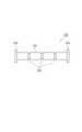
- the radiation detector 100 described in Patent Document 5 includes a columnar scintillator 101 in which a plurality of striped rough polishing portions 102 are formed on the side surface, and optically coupled to both ends of the columnar scintillator 101.
- the photodetectors 103 and 104 are provided.
- One of the methods for improving the detection accuracy of a radiation detector used in a PET apparatus is a method using information (hereinafter referred to as “detection position information”) about the position where radiation is detected in the scintillator.
- detection position information information about the position where radiation is detected in the scintillator.
- a method for obtaining the detected position information for example, there is a method in which the scintillator is optically separated into a plurality of regions and the region where the scintillation light is generated is specified.
- a method of stacking a plurality of scintillators on the PMT by providing an offset along the in-plane direction of the scintillator end face there is a method of stacking a plurality of scintillators on the PMT by providing an offset along the in-plane direction of the scintillator end face.
- a plurality of scintillator cells are formed by providing grooves on the end face of one scintillator crystal using a diamond cutter, and a predetermined offset is provided on the end face opposite to the end face.
- the scintillator cell is formed.
- such a scintillator has a complicated structure. Therefore, it takes time and money to manufacture the scintillator.
- FIG. 13 there is a method in which a comb-shaped reflector 112 is disposed between the scintillator cells 111 in order to optically separate the respective scintillator cells 111.
- the scintillator 110 when scintillation light is generated on the upper side of the scintillator cell 111, the scintillation light is scattered in the X direction.
- the scintillation light when scintillation light is generated below the scintillator cell 111, the scintillation light is scattered in the Y direction.
- the position where the scintillation light is generated can be calculated based on the direction and range in which the scintillation light is diffused.
- a method of calculating detection position information based on a ratio between a signal amplitude output from a photodetector provided at one end of the scintillator and a signal amplitude output from a photodetector provided at the other end is.
- the detection position information can be detected as spatially continuous information.
- the inside of the scintillator cell is optically almost homogeneous, the ratio of the light output at both ends depending on the light emission position in the scintillator cell tends to be small, and the detection position accuracy tends to be poor.
- a groove 123 is formed on the surface of the scintillator 121 in the longitudinal direction of the scintillator.
- There is a method of arranging them at equal intervals along the way for example, see Non-Patent Document 1).
- a process for forming the groove 123 is necessary. Therefore, manufacturing the scintillator 121 requires time and cost.
- the present invention has been made in view of the above-described problems, and an object of the present invention is to provide a radiation detector that can be easily manufactured and can realize good position detection characteristics.
- a radiation detector is a radiation detector that detects radiation, and includes a first end surface, a second end surface opposite to the first end surface, and a second end surface from the first end surface side.
- a scintillator having a plurality of light scattering surfaces spaced apart from each other along a first direction toward the end face side of the first optical detector, a first photodetector optically coupled to the first end face, A second light detector optically coupled to the two end faces, wherein the light scattering surface is formed to intersect the first direction, and the light scattering surface irradiates the inside of the scintillator with laser light.
- the first photodetector is optically coupled to the first end face of the scintillator
- the second photodetector is optically coupled to the second end face.
- the light scattering surface may be formed by irradiating the inside of the scintillator with laser light.
- a laser beam processing method for forming the light scattering surface the light scattering surface forming process can be automated. This laser beam processing method can be performed more simply than the method of polishing the surface of the scintillator or providing a groove on the surface of the scintillator. Therefore, the radiation detector described above can be easily manufactured.
- the modified region of the radiation detector may be composed of a plurality of modified spots that overlap each other. With such a configuration, a light scattering surface having a modified region that scatters scintillation light can be suitably formed.
- the light scattering surface of the radiation detector may have a modified region formed on the entire surface of the light scattering surface.
- the light scattering surface of the radiation detector has a first region in which a modified region is formed and a second region in which the modified region is not formed, and the second region is surrounded by the first region. It may be.
- the scintillation light generated by the absorption of radiation varies depending on the absorbed energy, hundreds to thousands of photons are generated, so if this part of the light is affected by this scattering surface, it will reach both ends. Since the light to be affected will be affected, the same effect can be brought about. Therefore, even when the scintillator is thick, even if the region where it is difficult to form the modified region exists on the light scattering surface due to such a configuration, the distance from the laser incident surface of the scintillator is long.
- a plurality of light scattering surfaces can be suitably formed. Further, since it is not necessary to form a modified region on the entire surface of the light scattering surface, the radiation detector can be easily manufactured.
- the light scattering surface of the radiation detector includes a plurality of third regions in which modified regions are formed and a plurality of fourth regions in which modified regions are not formed. These areas may be arranged in a checkered pattern.
- the first modified end surface has a quadrangular shape, the light scattering surface extends in a direction along one diagonal line on the first end surface, and the first end surface. And a second modified region extending in a direction along another diagonal line.
- the light scattering surface has a plurality of modified regions extending in the second direction, and the modified regions are spaced from each other along a direction substantially orthogonal to the second direction. It may be arranged open.
- the first end face may be a quadrangular shape
- the light scattering surface may have four modified regions
- the modified regions may be disposed at each of the four corners of the light scattering surface.
- the light scattering surface may have a modified region extending in a direction along a part or all of the edge of the light scattering surface.
- the area of the modified region on the light scattering surface is set to a predetermined value.
- the ratio of the scintillation light distributed to the first photodetector and the second photodetector can be set to a predetermined value.
- the amount of light reaching the photodetector can be set to an arbitrary magnitude, so that even better position detection characteristics can be realized.
- the radiation detector of the present invention it can be easily manufactured and a good position detection characteristic can be realized.
- FIG. 1 It is a perspective view which shows the external appearance and internal structure of the radiation detector which concern on 1st Embodiment. It is a figure for demonstrating the effect of the radiation detector which concerns on 1st Embodiment. It is a figure which shows the structure of the laser processing apparatus used in the process of manufacturing a scintillator. It is a flowchart which shows the method of forming a light-scattering surface using a laser processing apparatus. It is a perspective view which shows the external appearance and internal structure of the radiation detector which concern on 2nd Embodiment. It is a figure for demonstrating the effect of the radiation detector which concerns on 2nd Embodiment. It is a perspective view which shows the external appearance and internal structure of the radiation detector which concern on the modification 1. FIG.
- (A) is a figure which shows the structure of the light-scattering surface of the radiation detector which concerns on the modification 2
- (b) is a figure which shows the structure of the light-scattering surface of the radiation detector which concerns on the modification 3.
- (A) is a figure which shows the structure of the light-scattering surface of the radiation detector which concerns on the modification 4
- (b) is a figure which shows the structure of the light-scattering surface of the radiation detector which concerns on the modification 5.
- 1 is a perspective view illustrating a configuration of a radiation detector unit according to Embodiment 1.
- FIG. It is a side view which shows the structure of the radiation detector unit which concerns on Example 2.
- FIG. is a side view which shows the structure of the conventional radiation detector.
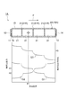
- FIG. 1 is a perspective view showing an overview and an internal configuration of a radiation detector 1A according to the first embodiment.
- the radiation detector 1A according to the present embodiment is optically coupled to the scintillator 2A, the first photodetector 12 optically coupled to the first end surface 11 of the scintillator 2A, and the second end surface 13.
- the second photodetector 14 and the reflection unit 19 are provided.
- the scintillator 2 ⁇ / b> A is a member for providing scintillation light to the first photodetector 12 and the second photodetector 14.
- the scintillator 2A is composed of a crystal lump 10A that generates scintillation light by the incidence of radiation such as gamma rays.
- the crystal lump 10A has a substantially rectangular parallelepiped outer shape.
- the scintillator 2A absorbs the radiation incident on the crystal lump 10A and generates scintillation light having an intensity corresponding to the dose.
- the crystal lump 10A includes, for example, Bi 4 Ge 3 O 12 (BGO), Ce 2 doped Lu 2 SiO 5 (LSO), Lu 2 (1-X) Y 2X SiO 5 (LYSO), Gd 2 SiO 5 (GSO). ), Pr doped LuAG (Lu 3 Al 5 O 12 ), Ce doped LaBr 3 (LaBr 3 ), Ce doped LaCl 3 (LaCl 3 ), Ce doped Lu 0.7 It is preferably composed of any crystal such as Y 0.3 AlO 3 (LuYAP).
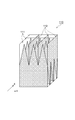
- the scintillator 2 ⁇ / b> A includes a plurality of light scattering surfaces 21 and a plurality of light emitting regions 31.
- the scintillator 2 ⁇ / b> A is separated into a plurality of light emitting regions 31 by a plurality of light scattering surfaces 21.
- the plurality of light scattering surfaces 21 are formed at intervals from each other along the first direction P from the first end surface 11 toward the second end surface 13.
- the plurality of light scattering surfaces 21 are formed so as to intersect the first direction P.
- These light scattering surfaces 21 have the same planar shape as the first end surface 11 or the second end surface 13 of the scintillator 2A.
- three light scattering surfaces 21 are formed in the scintillator 2A shown in FIG. 1, the present invention is not limited to this. Four or more light scattering surfaces 21 may be formed.
- the light scattering surface 21 is constituted by a modified region 21R formed on the entire surface of the light scattering surface 21.
- the modified region 21R is constituted by a plurality of modified spots formed so as to overlap each other by irradiation with laser light, and the plurality of modified spots form an optical scattering surface.
- the modified spot has, for example, a void shape. Since the modified region 21R does not block or absorb scintillation light, even if the modified region 21R is formed on the entire surface of the light scattering surface 21, part of the scintillation light is transmitted.
- the light scattering surface 21 has a property that the transmittance of the scintillation light varies depending on the incident angle to the light scattering surface 21.
- the transmittance of the light scattering surface 21 changes according to the incident angle of the scintillation light. For example, when the scintillation light enters the light scattering surface 21 vertically, the incident scintillation light is almost transmitted. On the other hand, as the incident angle increases, the transmittance decreases as compared with the case where the incident angle is perpendicular.
- the first photodetector 12 and the second photodetector 14 are, for example, a semiconductor photodetector such as a photomultiplier tube, an avalanche photodiode (APD), or an MPPC (Multi-Pixel Photo Counter). It is suitably configured.
- the MPPC is a photon counting device composed of a plurality of Geiger mode APD pixels.
- the radiation detector 1 ⁇ / b> A of the present embodiment includes a first photodetector 12 and a second photodetector 14.
- the first photodetector 12, which is one of the photodetectors, is attached on the crystal lump 10A so as to face the first end face 11 of the crystal lump 10A.
- the second photodetector 14 which is another photodetector is mounted on the crystal lump 10 so as to face the second end face 13 of the crystal lump 10A.
- the first photodetector 12 is optically coupled to the first end face 11 of the crystal lump 10A
- the second photodetector 14 is optically coupled to the second end face 13 of the crystal lump 10A.
- the reflection portion 19 is provided so as to cover a side surface extending between the first end surface 11 and the second end surface 13 in the scintillator 2A.
- the reflecting portion 19 is preferably composed of, for example, any member such as Teflon tape (Teflon is a registered trademark), barium sulfate, aluminum oxide, titanium oxide, an enhanced specular reflector (ESR) film, and a polyester film.
- the graph G1 in FIG. 2 shows the relationship between the light emission position of the scintillation light in the scintillator 2A and the light output output from the first photodetector 12.
- the graph G2 shows the relationship between the light emission position of the scintillation light in the scintillator 2A and the light output output from the second photodetector 14.
- Graph G3 shows the relationship between the ratio of light output and the emission position of scintillation light.
- the ratio of the light output is the ratio between the light output output from the first photodetector 12 and the light output output from the second photodetector 14.
- the first photodetector 12 is optically coupled to the first end face 11 of the scintillator 2A.
- the second photodetector 14 is optically coupled to the second end face 13.
- the scintillator 2A has a plurality of light scattering surfaces 21. With the plurality of light scattering surfaces 21, the amount of light reaching the first photodetector 12 and the second photodetector 14 can be attenuated step by step. For example, when scintillation light is generated at the position F1 in the scintillator 2A, the scintillation light passes through the light scattering surface 21 and reaches the first photodetector 12. Since part of the scintillation light is scattered when passing through the light scattering surface 21, the amount of light is reduced after transmission through the light scattering surface 21 than before transmission. Then, the optical output H1 is output from the first photodetector 12. On the other hand, the optical output H2 is output from the second photodetector 14.
- the light output ratio H3 has a predetermined difference that can be easily discriminated for each light emitting region 31, as shown in the graph G3. Accordingly, it is possible to accurately identify the light emitting region 31 where the scintillation light is generated based on the light output ratio H3, and the radiation detector 1A can realize a good position detection characteristic.
- the light scattering surface 21 is formed by irradiating the inside of the scintillator 2A with laser light.
- a laser beam processing method for forming the light scattering surface 21 it is possible to automate the process of forming the light scattering surface 21.
- This laser beam processing method can be performed more simply than the method of polishing the surface of the scintillator or providing a groove on the surface of the scintillator. Therefore, the radiation detector 1A described above can be easily manufactured.
- a modified region 21R is formed on the entire surface of the light scattering surface 21.
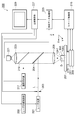
- FIG. 3 is a diagram for explaining one process of manufacturing the scintillator 2A including a plurality of modified regions 21R, and shows the configuration of the laser processing apparatus 200 used in this process.
- the laser processing apparatus 200 includes a laser light source 201 that generates laser light L, a laser light source control unit 202 that controls the laser light source 201 in order to adjust the output and pulse width of the laser light L, and the optical path of the laser light L. , A dichroic mirror 204 having a function of reflecting the laser light L and changing the direction of the optical axis of the laser light L by 90 °, and the laser light L reflected by the dichroic mirror 204 A condensing lens 205, a mounting table 207 on which the crystal lump 10A irradiated with the laser light L collected by the condensing lens 205 is mounted, and the mounting table 207 is moved in the X-axis direction.
- the Z-axis direction is the direction of the focal depth of the laser light L incident on the crystal lump 10A. Therefore, by moving the Z-axis stage 213 in the Z-axis direction, the condensing point D of the laser light L can be adjusted inside the crystal lump 10A. Further, each movement of the condensing point D in the X-axis direction and the Y-axis direction is performed by moving the crystal lump 10A in the X-axis direction and the Y-axis direction by the X-axis stage 209 and the Y-axis stage 211, respectively.
- the pulse laser beam examples include femtosecond pulse laser beam and picosecond pulse laser beam. Since femtosecond and picosecond laser pulses absorb laser energy faster than the thermal diffusion rate, there is little influence of heat on the periphery of the workpiece, and high electric field density can be easily obtained. It is possible to suitably form a modified region 21R such as a change in refractive index that does not cause the problem.
- the nanosecond laser pulse requires irradiation energy several times that of a femtosecond or picosecond laser pulse in order to obtain an electric field density equal to or higher than the processing threshold, and the laser energy is easily stored in the material to be processed. Further contrivance is required to form the modified region 21R such as a change in refractive index.
- the laser processing apparatus 200 further includes an observation light source 217 that generates visible light to illuminate the crystal lump 10A mounted on the mounting table 207 with visible light, and the same optical axis as the dichroic mirror 204 and the condensing lens 205. And a visible light beam splitter 219 disposed above.
- a dichroic mirror 204 is disposed between the beam splitter 219 and the condensing lens 205.
- the beam splitter 219 has a function of reflecting about half of visible light and transmitting the other half, and is arranged so as to change the direction of the optical axis of visible light by 90 °.
- the laser processing apparatus 200 further includes an imaging data processing unit 225 to which imaging data output from the CCD camera 221 is input, an overall control unit 227 that controls the entire laser processing apparatus 200, and a monitor 229.
- the imaging data processing unit 225 calculates focus data for focusing the visible light generated by the observation light source 217 on the crystal lump 10A based on the imaging data.
- the stage control unit 215 controls the movement of the Z-axis stage 213 based on the focus data so that the visible light is focused on the crystal lump 10A. Therefore, the imaging data processing unit 225 functions as an autofocus unit.
- the imaging data processing unit 225 calculates image data such as an enlarged image of the crystal lump 10A based on the imaging data. This image data is sent to the overall control unit 227, where various processes are performed by the overall control unit 227 and sent to the monitor 229. Thereby, an enlarged image or the like is displayed on the monitor 229.
- the condensing point D of the laser beam L for forming the modified region 21R inside the crystal lump 10A is the initial processing position of one modified region 21R on or inside the crystal lump 10A.
- the crystal lump 10A is moved by the X-axis stage 209, the Y-axis stage 211, and the Z-axis stage 213 (S103).
- the shutter 203 is opened and the laser beam L is irradiated to modify (amorphize) the scintillator material in the condensing portion, thereby forming a modified spot inside the crystal lump 10A.
- This modified spot is, for example, at least one of a region having a refractive index smaller than the surroundings, a region that scatters light, and a region that constitutes a diffractive lens. Thereafter, the shutter 203 of the laser light L is closed (S109).
- FIG. 5 is a diagram illustrating an overview and an internal configuration of the radiation detector 1B according to the second embodiment.
- the radiation detector 1 ⁇ / b> B according to the present embodiment includes a scintillator 2 ⁇ / b> B having a plurality of light scattering surfaces 22, a first photodetector 12, a second photodetector 14, and a reflection unit 19.
- the radiation detector 1B according to the present embodiment is different from the radiation detector 1A according to the first embodiment in that it has a light scattering surface 22 different from the light scattering surface 21 according to the first embodiment. .
- a plurality of light scattering surfaces 22 are formed inside the crystal lump 10B of the scintillator 2B.
- the light scattering surface 22 includes a modified region 22R (first region) and a non-modified region 22N (second region) in which the modified region 22R is not formed.
- the modified region 22R is preferably formed by irradiating the inside of the crystal lump 10B with laser light.
- the non-modified region 22N is surrounded by the modified region 22R.
- the radiation detector 1B including the scintillator 2B in which a plurality of light scattering surfaces 22 are formed as in the present embodiment it is possible to suitably obtain the effects of the radiation detector 1A according to the first embodiment described above. it can.
- the present embodiment even when the region where the formation of the modified region 22R is difficult exists on the light scattering surface 22 because the distance from the side surface 15 that is the laser incident surface of the scintillator 2B is long, It is not necessary to form the modified region 22R in that place. Therefore, a plurality of light scattering surfaces 22 can be formed suitably. Further, it is not necessary to form the modified region 22R on the entire surface of the light scattering surface 22. Therefore, the processing time for forming the light scattering surface 22 can be shortened.
- FIG. 6 shows the relationship between the light emission position of the scintillation light in the scintillator 2B and the light output detected by the first photodetector 12.
- a graph G4 shows the relationship between the light emission position of the scintillation light and the light output in the scintillator 2B.
- the graph G5 shows the relationship between the light emission position of the scintillation light in the scintillator 2A according to the first embodiment and the light output detected by the first photodetector 12.
- the graph G6 shows the relationship between the light emission position of the scintillation light in the scintillator having no light scattering surface and the light output detected by the first photodetector 12.
- the degree to which scintillation light is scattered when passing through the light scattering surface is considered to be basically affected by the area of the modified region on the light scattering surface. Therefore, as shown in the graph G5, in the scintillator 2A having the light scattering surface 21 in which the modified region 21R is formed on the entire surface, the scintillation light generated in the region close to the first photodetector 12 is detected by the first light detection.
- a light output difference D2 that is a difference between the light output when detected by the detector 12 and the light output when the first photodetector 12 detects scintillation light generated in a region far from the first photodetector 12 Is the largest.
- the light output difference D3 is the smallest in the scintillator having no light scattering surface.
- the area of the modified region 22R of the light scattering surface 22 according to the present embodiment can be set to an arbitrary value. Therefore, in the scintillator 2B having the light scattering surface 22 according to the present embodiment, the light output difference D1 can be set so as to have a size between the light output difference D2 and the light output difference D3.
- the amount of light reaching the first photodetector 12 and the second photodetector 14 can be freely controlled, so the first photodetector Based on the ratio of the light outputs detected by the second light detector 12 and the second light detector 14, it is possible to specify the light emitting region with higher accuracy, and the radiation detector 1B can realize good position detection characteristics.
- the non-modified region 22N is surrounded by the modified region 22R.
- the shape and arrangement of the modified region 22R and the non-modified region 22N are not limited to this, and various modifications are possible.
- FIG. 7 is a diagram illustrating an overview and an internal configuration of the radiation detector 1C according to the first modification.
- the radiation detector 1 ⁇ / b> C according to this modification includes a scintillator 2 ⁇ / b> C having a plurality of light scattering surfaces 23, a first photodetector 12, a second photodetector 14, and a reflector 19.
- the radiation detector 1C according to this modification is different from the radiation detector 1B according to the second embodiment in that the radiation detector 1C has a light scattering surface 23 different from the light scattering surface 22 according to the second embodiment. .
- a plurality of light scattering surfaces 23 are formed inside the crystal lump 10C of the scintillator 2C.
- the light scattering surface 23 has a plurality of modified regions 23R (a plurality of third regions) and a plurality of non-modified regions 23N (a plurality of fourth regions) in which the modified regions 23R are not formed. ing.
- the plurality of modified regions 23R are preferably formed by irradiating the inside of the crystal lump 10C with laser light.
- the modified region 23R and the non-modified region 23N are arranged in a checkered pattern.
- the radiation detector 1C including the scintillator 2C in which a plurality of light scattering surfaces 23 are formed as in the present modification it is possible to suitably obtain the effects of the radiation detector 1B according to the second embodiment described above. it can.
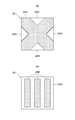
- Fig.8 (a) is a figure which shows the structure of the light-scattering surface 24 of the radiation detector which concerns on the modification 2 of the radiation detector 1B which concerns on 2nd Embodiment mentioned above.
- the first end face 11 (see FIG. 5) has a quadrangular shape.
- the light scattering surface 24 is formed by a modified region extending in a direction along one diagonal line in the first end surface 11 and a modified region extending in a direction along another diagonal line in the first end surface 11.
- the modified region 24R is configured. Even in the case of a radiation detector including the light scattering surface 24 having the modified region 24R as in the present modification, the effects of the invention according to the second embodiment described above can be suitably obtained.
- FIG. 8B is a diagram illustrating a configuration of the light scattering surface 25 of the radiation detector according to the third modification of the second embodiment described above.
- the light scattering surface 25 has a plurality of modified regions 25R extending in a predetermined direction (second direction) within the surface of the light scattering surface 25, and the modified regions 25R are substantially perpendicular to the predetermined direction. Are spaced apart from each other.
- Each of the plurality of modified regions 25R is surrounded by a non-modified region 25N where the modified region 25R is not formed. Even in the case of a radiation detector including the light scattering surface 25 having the modified region 25R as in the present modification, the effect of the invention according to the second embodiment described above can be suitably obtained.
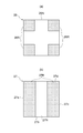
- Fig.9 (a) is a figure which shows the structure of the light-scattering surface 26 of the radiation detector which concerns on the modification 4 of 2nd Embodiment mentioned above.
- the first end face 11 (see FIG. 5) has a quadrangular shape.
- the light scattering surface 26 has four modified regions 26R, and the modified regions 26R are disposed at the four corners of the light scattering surface 26, respectively.
- each of the four modified regions 26R has a substantially square shape.
- the non-modified region 26N in which the modified region 26R is not formed is formed in a substantially cross shape. Even in the case of a radiation detector including the light scattering surface 26 having the modified region 26R as in the present modification, the effects of the invention according to the third embodiment described above can be suitably obtained.
- FIG. 9B is a diagram illustrating a configuration of the light scattering surface 27 of the radiation detector according to the fifth modification of the second embodiment described above.
- the light scattering surface 27 has a modified region 27 ⁇ / b> R extending in a direction along part or all of the edge of the light scattering surface 27.
- the modified region 27R includes, for example, one of the four edges 27a to 27d of the light scattering surface 27 that has a rectangular shape, and one edge 27a and the other edge 27c opposite to the one edge 27a. It may be formed.
- the modified region 27R and the non-modified region 27N in which the modified region is not formed are arranged in a striped pattern. Even in the case of a radiation detector including the light scattering surface 27 having the modified region 27R as in this modification, the effects of the invention according to the second embodiment described above can be suitably obtained.
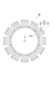
- FIG. 10 is a perspective view showing a configuration of a radiation detector unit 50 that constitutes a part of the PET apparatus.
- the radiation detector unit 50 includes a plurality of radiation detector arrays 51.
- the radiation detector array 51 includes a scintillator array 52, a first photodetector array 53, and a second photodetector array 54.
- the first photodetector 12 constituting the first photodetector array 53 is optically coupled to the first end face 11 of the scintillator 2A (see FIG. 1) constituting the scintillator array 52, and the second end face. 13, the second photodetector 14 constituting the second photodetector array 54 is optically coupled to form the radiation detector 1A according to the first embodiment.
- Each of the plurality of radiation detector arrays 51 is arranged along the circumference of a circle centered on the measurement target T.
- the radiation detector array 51 is arranged so that the side surface 52a of the scintillator array 52 and the measurement target T face each other.
- a set of radiation detector arrays 51 that perform coincidence counting includes one radiation detector array 51 and a plurality of other radiation detectors on the opposite side of the radiation detector array 51. And an instrument array 51.
- FIG. 11 is a diagram showing a configuration of a radiation detector unit 60 that constitutes a part of the PET apparatus.
- the radiation detector unit 60 includes a plurality of radiation detector arrays 61.
- the radiation detector array 61 includes a scintillator array 62, a first photodetector array 63, and a second photodetector array 64.
- the first photodetector 12 constituting the first photodetector array 63 is optically coupled to the first end face 11 of the scintillator 2A (see FIG. 1) constituting the scintillator array 62, and the second end face. 13, the second photodetector 14 constituting the second photodetector array 64 is optically coupled to form the radiation detector 1A according to the first embodiment.
- the radiation detector of the present invention it can be easily manufactured and a good position detection characteristic can be realized.
- second photodetector array 103, 104, 122, 124 ... Photodetector, 200 ... Laser processing apparatus, 201 ... Laser light source, 202 ... Laser light source controller, 203 ... Shutter, 204 ... Dichroic mirror, 205 ... Condensing lens, 207 ... Place, 209 ... X-axis stage 211 ... Y-axis stage, 213 ... Z-axis stage, 215 ... stage controller, 217 ... light source for observation, 219 ... beam splitter, 221 ... CCD camera, 223 ... imaging lens, 225 ... imaging data processor, 227 ... whole Control unit, 229 ... monitor, D ... condensing point, P ... first direction.
Landscapes
- Physics & Mathematics (AREA)
- Health & Medical Sciences (AREA)
- Life Sciences & Earth Sciences (AREA)
- General Physics & Mathematics (AREA)
- High Energy & Nuclear Physics (AREA)
- Molecular Biology (AREA)
- Spectroscopy & Molecular Physics (AREA)
- Chemical & Material Sciences (AREA)
- Crystallography & Structural Chemistry (AREA)
- Measurement Of Radiation (AREA)
- Nuclear Medicine (AREA)
Abstract
Description
図1は、第1実施形態に係る放射線検出器1Aの概観と内部構成とを示す斜視図である。本実施形態に係る放射線検出器1Aは、シンチレータ2Aと、シンチレータ2Aの第1の端面11に光学的に結合される第1の光検出器12と、第2の端面13に光学的に結合される第2の光検出器14と、反射部19とを備えている。
図5は、第2実施形態に係る放射線検出器1Bの概観と内部構成とを示す図である。本実施形態に係る放射線検出器1Bは、複数の光散乱面22を有するシンチレータ2Bと、第1の光検出器12及び第2の光検出器14と、反射部19とを備える。本実施形態に係る放射線検出器1Bは、第1実施形態に係る光散乱面21とは異なる光散乱面22を有している点で、第1実施形態に係る放射線検出器1Aと異なっている。なお、第1の光検出器12及び第2の光検出器14、及び反射部19の構成及び配置は、上述した第1実施形態に係る放射線検出器1Aと同様であるため、詳細な説明は省略する。
図7は、変形例1に係る放射線検出器1Cの概観と内部構成とを示す図である。本変形例に係る放射線検出器1Cは、複数の光散乱面23を有するシンチレータ2Cと、第1の光検出器12及び第2の光検出器14と、反射部19とを備える。本変形例に係る放射線検出器1Cは、第2実施形態に係る光散乱面22とは異なる光散乱面23を有している点で、第2実施形態に係る放射線検出器1Bと異なっている。なお、第1の光検出器12及び第2の光検出器14、及び反射部19の構成及び配置は、上述した第2実施形態に係る放射線検出器1Bと同様であるため、詳細な説明は省略する。
図8(a)は、上述した第2実施形態に係る放射線検出器1Bの変形例2に係る放射線検出器の光散乱面24の構成を示す図である。第1の端面11(図5参照)は四角形状である。更に、光散乱面24は、第1の端面11における一の対角線に沿った方向に延びた改質領域と、第1の端面11における他の対角線に沿った方向に延びた改質領域とにより構成される改質領域24Rを有している。本変形例のように、改質領域24Rを有する光散乱面24を備える放射線検出器であっても、上述した第2実施形態に係る発明の効果を好適に得ることができる。
図8(b)は、上述した第2実施形態の変形例3に係る放射線検出器の光散乱面25の構成を示す図である。光散乱面25は、光散乱面25の面内における所定の方向(第2の方向)に延びた複数の改質領域25Rを有し、改質領域25Rは、所定の方向と略直交する方向に沿って互いに間隔をあけて配置されている。複数の改質領域25Rのそれぞれは、改質領域25Rが形成されていない非改質領域25Nに囲まれている。本変形例のように、改質領域25Rを有する光散乱面25を備える放射線検出器であっても、上述した第2実施形態に係る発明の効果を好適に得ることができる。
図9(a)は、上述した第2実施形態の変形例4に係る放射線検出器の光散乱面26の構成を示す図である。第1の端面11(図5参照)は四角形状である。光散乱面26は、4つの改質領域26Rを有し、改質領域26Rは、光散乱面26の四隅のそれぞれに配置されている。例えば、4つの改質領域26Rのそれぞれは、略正方形状である。改質領域26Rが形成されていない非改質領域26Nは、略十字状に形成されている。本変形例のように、改質領域26Rを有する光散乱面26を備える放射線検出器であっても、上述した第3実施形態に係る発明の効果を好適に得ることができる。
図9(b)は、上述した第2実施形態の変形例5に係る放射線検出器の光散乱面27の構成を示す図である。光散乱面27は、光散乱面27の縁部の一部又は全部に沿った方向に延びた改質領域27Rを有する。改質領域27Rは、例えば、四角形状である光散乱面27の4つの縁部27a~27dのうち、一の縁部27aと、一の縁部27aとは反対側の他の縁部27cとに形成されていてもよい。本変形例では、改質領域27Rと、改質領域が形成されていない非改質領域27Nとは、縞状に配置されている。本変形例のように、改質領域27Rを有する光散乱面27を備える放射線検出器であっても、上述した第2実施形態に係る発明の効果を好適に得ることができる。
次に、上述した放射線検出器1Aを用いた実施例1について説明する。図10は、PET装置の一部を構成する放射線検出器ユニット50の構成を示す斜視図である。この放射線検出器ユニット50は、複数の放射線検出器アレイ51を備えている。放射線検出器アレイ51は、シンチレータアレイ52と、第1の光検出器アレイ53と、第2の光検出器アレイ54とを備えている。シンチレータアレイ52を構成するシンチレータ2A(図1参照)の第1の端面11に、第1の光検出器アレイ53を構成する第1の光検出器12が光学的に結合され、第2の端面13に第2の光検出器アレイ54を構成する第2の光検出器14が光学的に結合されて第1実施形態に係る放射線検出器1Aを構成している。
次に、上述した放射線検出器1Aを用いた実施例2について説明する。図11は、PET装置の一部を構成する放射線検出器ユニット60の構成を示す図である。この放射線検出器ユニット60は、複数の放射線検出器アレイ61を備えている。放射線検出器アレイ61は、シンチレータアレイ62と、第1の光検出器アレイ63と、第2の光検出器アレイ64とを備えている。シンチレータアレイ62を構成するシンチレータ2A(図1参照)の第1の端面11に、第1の光検出器アレイ63を構成する第1の光検出器12が光学的に結合され、第2の端面13に第2の光検出器アレイ64を構成する第2の光検出器14が光学的に結合されて第1実施形態に係る放射線検出器1Aを構成している。
Claims (9)
- 放射線を検出する放射線検出器であって、
第1の端面、前記第1の端面の反対側にある第2の端面、及び前記第1の端面側から前記第2の端面側に向かう第1の方向に沿って互いに間隔をあけて形成された複数の光散乱面を有するシンチレータと、
前記第1の端面と光学的に結合された第1の光検出器と、
前記第2の端面と光学的に結合された第2の光検出器と、を備え、
前記光散乱面は、前記第1の方向と交わるように形成され、
前記光散乱面は、前記シンチレータの内部にレーザ光を照射することにより形成された一又は複数の改質領域を含む放射線検出器。 - 前記改質領域は、互いに重なり合う複数の改質スポットから構成されている請求項1に記載の放射線検出器。
- 前記光散乱面は、前記改質領域が前記光散乱面の全面に形成されて成る請求項1又は2に記載の放射線検出器。
- 前記光散乱面は、前記改質領域が形成された第1の領域と前記改質領域が形成されていない第2の領域とを有し、前記第2の領域は前記第1の領域によって囲まれている請求項1又は2に記載の放射線検出器。
- 前記光散乱面は、前記改質領域が形成された複数の第3の領域と前記改質領域が形成されていない複数の第4の領域とを有し、前記第3の領域と前記第4の領域とが市松模様状に配置されている請求項1又は2に記載の放射線検出器。
- 前記第1の端面は四角形状であり、前記光散乱面は、前記第1の端面における一の対角線に沿った方向に延びた第1の前記改質領域と、前記第1の端面における他の対角線に沿った方向に延びた第2の前記改質領域とを有する請求項1又は2に記載の放射線検出器。
- 前記光散乱面は、第2の方向に延びた前記複数の改質領域を有し、前記複数の改質領域は、前記第2の方向と略直交する方向に沿って互いに間隔をあけて配置されている請求項1又は2に記載の放射線検出器。
- 前記第1の端面は四角形状であり、前記光散乱面は4つの前記改質領域を有し、前記改質領域は前記光散乱面の四隅のそれぞれに配置されている請求項1又は2に記載の放射線検出器。
- 前記光散乱面は、前記光散乱面の縁部の一部又は全部に沿った方向に延びた前記改質領域を有する請求項1又は2に記載の放射線検出器。
Priority Applications (2)
| Application Number | Priority Date | Filing Date | Title |
|---|---|---|---|
| JP2012555774A JP6012475B2 (ja) | 2011-02-02 | 2012-01-13 | 放射線検出器、放射線検出器の製造方法及び放射線検出方法 |
| US13/983,167 US8809794B2 (en) | 2011-02-02 | 2012-01-13 | Radiation detector |
Applications Claiming Priority (2)
| Application Number | Priority Date | Filing Date | Title |
|---|---|---|---|
| JP2011-020942 | 2011-02-02 | ||
| JP2011020942 | 2011-02-02 |
Publications (1)
| Publication Number | Publication Date |
|---|---|
| WO2012105292A1 true WO2012105292A1 (ja) | 2012-08-09 |
Family
ID=46602513
Family Applications (1)
| Application Number | Title | Priority Date | Filing Date |
|---|---|---|---|
| PCT/JP2012/050609 Ceased WO2012105292A1 (ja) | 2011-02-02 | 2012-01-13 | 放射線検出器 |
Country Status (3)
| Country | Link |
|---|---|
| US (1) | US8809794B2 (ja) |
| JP (1) | JP6012475B2 (ja) |
| WO (1) | WO2012105292A1 (ja) |
Cited By (12)
| Publication number | Priority date | Publication date | Assignee | Title |
|---|---|---|---|---|
| WO2013099162A1 (ja) * | 2011-12-28 | 2013-07-04 | 学校法人早稲田大学 | 放射線検出器 |
| WO2015040527A1 (en) * | 2013-09-18 | 2015-03-26 | Koninklijke Philips N.V. | Laser etched scintillation crystals for increased performance |
| JP2016031289A (ja) * | 2014-07-29 | 2016-03-07 | 浜松ホトニクス株式会社 | 放射線検出器 |
| JP2016145820A (ja) * | 2015-01-30 | 2016-08-12 | 浜松ホトニクス株式会社 | 放射線検出器 |
| JP2016145819A (ja) * | 2015-01-30 | 2016-08-12 | 浜松ホトニクス株式会社 | 放射線検出器 |
| WO2016175318A1 (ja) * | 2015-04-30 | 2016-11-03 | 浜松ホトニクス株式会社 | シンチレータ体、放射線検出器及びシンチレータ体の製造方法 |
| US9529096B2 (en) | 2015-01-30 | 2016-12-27 | Hamamatsu Photonics K.K. | Radiation detector |
| US9753149B2 (en) | 2015-01-30 | 2017-09-05 | Hamamatsu Photonics K.K. | Radiation detector |
| US9804277B2 (en) | 2015-01-30 | 2017-10-31 | Hamamatsu Photonics K.K. | Radiation detector |
| US9945967B2 (en) | 2015-01-30 | 2018-04-17 | Hamamatsu Photonics K.K. | Radiation detector |
| US10094937B2 (en) | 2015-01-30 | 2018-10-09 | Hamamatsu Photonics K.K. | Radiation detector |
| WO2024111385A1 (ja) * | 2022-11-24 | 2024-05-30 | 国立研究開発法人量子科学技術研究開発機構 | シンチレータアレイ、放射線検出装置、及び陽電子放出断層撮影装置 |
Families Citing this family (11)
| Publication number | Priority date | Publication date | Assignee | Title |
|---|---|---|---|---|
| WO2015130770A1 (en) * | 2014-02-26 | 2015-09-03 | Saint-Gobain Ceramics & Plastics, Inc. | Scintillator array and methods of forming a scintillator array and a radiation detector |
| DE102014224449A1 (de) * | 2014-11-28 | 2016-06-02 | Forschungszentrum Jülich GmbH | Szintillationsdetektor mit hoher Zählrate |
| US9709684B2 (en) * | 2014-12-15 | 2017-07-18 | General Electric Company | Systems and methods for scintillators having micro-crack surfaces |
| US9903961B1 (en) * | 2016-09-01 | 2018-02-27 | FMI Medical Systems Co., Ltd. | Photodetector array readout multiplexer having summing, pulse shaping, and dynamic-switching circuits |
| JP6707048B2 (ja) * | 2017-03-22 | 2020-06-10 | 富士フイルム株式会社 | マンモグラフィ装置 |
| US10208587B1 (en) * | 2017-08-28 | 2019-02-19 | General Electric Company | System and method for monitoring integrity of a wellbore |
| JP7109168B2 (ja) | 2017-09-13 | 2022-07-29 | 浜松ホトニクス株式会社 | 放射線位置検出方法、放射線位置検出器及びpet装置 |
| CN112068178B (zh) * | 2019-06-10 | 2023-08-29 | 睿生光电股份有限公司 | 放射线感测装置 |
| IT201900010638A1 (it) * | 2019-07-02 | 2021-01-02 | St Microelectronics Srl | Rilevatore di radiazione a scintillatore e dosimetro corrispondente |
| US12013503B2 (en) * | 2022-10-07 | 2024-06-18 | Cintilight, Llc | Lateral crystal photodiode readouts and switched diode networks for processing nuclear events |
| US12449554B2 (en) | 2023-10-05 | 2025-10-21 | Cintilight, Llc | Scintillator detectors and methods for positron emission tomography |
Citations (8)
| Publication number | Priority date | Publication date | Assignee | Title |
|---|---|---|---|---|
| JPS6375587A (ja) * | 1986-09-18 | 1988-04-05 | Hamamatsu Photonics Kk | ポジトロンct装置 |
| JPH0518390B2 (ja) * | 1986-12-11 | 1993-03-11 | Hamamatsu Hotonikusu Kk | |
| JPH06331748A (ja) * | 1993-05-21 | 1994-12-02 | Horiba Ltd | シンチレータおよびその製造法 |
| JP2007525652A (ja) * | 2003-05-30 | 2007-09-06 | シーティーアイ ペット システムズ インコーポレイテッド | レーザー技術による検知器コンポーネントの作製方法 |
| JP2009031132A (ja) * | 2007-07-27 | 2009-02-12 | Tohoku Univ | 放射線検出器 |
| JP2009270971A (ja) * | 2008-05-08 | 2009-11-19 | Hamamatsu Photonics Kk | シンチレータの製造方法および放射線位置検出器 |
| JP2010139383A (ja) * | 2008-12-11 | 2010-06-24 | Hamamatsu Photonics Kk | シンチレータ、放射線検出器、およびシンチレータの製造方法 |
| JP2010139375A (ja) * | 2008-12-11 | 2010-06-24 | Hamamatsu Photonics Kk | シンチレータ、放射線検出器、およびシンチレータの製造方法 |
Family Cites Families (19)
| Publication number | Priority date | Publication date | Assignee | Title |
|---|---|---|---|---|
| US3825758A (en) * | 1971-09-13 | 1974-07-23 | F Miraldi | Scintillation crystal |
| US5118934A (en) * | 1990-08-03 | 1992-06-02 | The United States Of America As Represented By The United States Department Of Energy | Fiber fed x-ray/gamma ray imaging apparatus |
| JP2939365B2 (ja) | 1991-07-15 | 1999-08-25 | 株式会社東芝 | ポンプの運転台数制御装置 |
| US5132539A (en) * | 1991-08-29 | 1992-07-21 | General Electric Company | Planar X-ray imager having a moisture-resistant sealing structure |
| DE69837429T2 (de) * | 1997-02-10 | 2007-12-06 | The University of Alberta, Simon Fraser University, the Univ. of Victoria, the Univ. of British Columbia, carrying on as Triumf, Vancouver | Unterteilter szintillationsdetektor zur feststellung der koordinaten von photoneninteraktionen |
| CA2492587A1 (en) * | 2002-07-17 | 2004-01-22 | Christian Joram | Gamma ray detector for positron emission tomography (pet) and single photon emmission computed tomography (spect) |
| US6989541B2 (en) * | 2003-05-30 | 2006-01-24 | General Dynamics Advanced Information Systems, Inc. | Coincident neutron detector for providing energy and directional information |
| US7238946B2 (en) * | 2003-06-27 | 2007-07-03 | Siemens Medical Solutions Usa, Inc. | Nuclear imaging system using scintillation bar detectors and method for event position calculation using the same |
| GB2418015B (en) * | 2004-05-24 | 2006-12-20 | Symetrica Ltd | Gamma ray spectrometers |
| WO2006071922A2 (en) * | 2004-12-29 | 2006-07-06 | Siemens Medical Solutions Usa, Inc. | Combined pet/mr imaging system and apd-bassed pet detector for use in simultaneous pet/mr imaging |
| US20070057194A1 (en) * | 2005-08-31 | 2007-03-15 | Ryan James M | Neutron and gamma-ray detection system |
| GB2437979B (en) * | 2006-05-12 | 2010-12-01 | Symetrica Ltd | Plastic scintillators |
| US7737408B2 (en) * | 2007-07-24 | 2010-06-15 | Siemens Medical Solutions Usa, Inc. | Monolithic scintillators with optical fiber read-out |
| JP5307673B2 (ja) * | 2009-09-28 | 2013-10-02 | 浜松ホトニクス株式会社 | シンチレータ、放射線検出器、及びシンチレータの製造方法 |
| CN105676258B (zh) * | 2009-10-07 | 2019-03-22 | 圣戈本陶瓷及塑料股份有限公司 | 检测目标辐射的系统和方法 |
| CN102655813B (zh) * | 2009-10-27 | 2015-08-12 | 华盛顿大学商业中心 | 用于辐射检测器晶体的光学界面图案形成 |
| US8426827B2 (en) * | 2010-02-10 | 2013-04-23 | Vega Grieshaber Kg | Automatic gain stabilization and temperature compensation for organic and/or plastic scintillation devices |
| KR101169708B1 (ko) * | 2010-04-26 | 2012-07-30 | 서강대학교산학협력단 | 큰 면적을 가진 마이크로셀로 구성된 gapd를 이용한 pet 검출기 모듈 |
| US8519349B2 (en) * | 2010-11-08 | 2013-08-27 | Nucsafe, Inc. | Scintillator panel having uniform output response |
-
2012
- 2012-01-13 WO PCT/JP2012/050609 patent/WO2012105292A1/ja not_active Ceased
- 2012-01-13 JP JP2012555774A patent/JP6012475B2/ja active Active
- 2012-01-13 US US13/983,167 patent/US8809794B2/en active Active
Patent Citations (8)
| Publication number | Priority date | Publication date | Assignee | Title |
|---|---|---|---|---|
| JPS6375587A (ja) * | 1986-09-18 | 1988-04-05 | Hamamatsu Photonics Kk | ポジトロンct装置 |
| JPH0518390B2 (ja) * | 1986-12-11 | 1993-03-11 | Hamamatsu Hotonikusu Kk | |
| JPH06331748A (ja) * | 1993-05-21 | 1994-12-02 | Horiba Ltd | シンチレータおよびその製造法 |
| JP2007525652A (ja) * | 2003-05-30 | 2007-09-06 | シーティーアイ ペット システムズ インコーポレイテッド | レーザー技術による検知器コンポーネントの作製方法 |
| JP2009031132A (ja) * | 2007-07-27 | 2009-02-12 | Tohoku Univ | 放射線検出器 |
| JP2009270971A (ja) * | 2008-05-08 | 2009-11-19 | Hamamatsu Photonics Kk | シンチレータの製造方法および放射線位置検出器 |
| JP2010139383A (ja) * | 2008-12-11 | 2010-06-24 | Hamamatsu Photonics Kk | シンチレータ、放射線検出器、およびシンチレータの製造方法 |
| JP2010139375A (ja) * | 2008-12-11 | 2010-06-24 | Hamamatsu Photonics Kk | シンチレータ、放射線検出器、およびシンチレータの製造方法 |
Cited By (17)
| Publication number | Priority date | Publication date | Assignee | Title |
|---|---|---|---|---|
| WO2013099162A1 (ja) * | 2011-12-28 | 2013-07-04 | 学校法人早稲田大学 | 放射線検出器 |
| WO2015040527A1 (en) * | 2013-09-18 | 2015-03-26 | Koninklijke Philips N.V. | Laser etched scintillation crystals for increased performance |
| EP3047308B1 (en) * | 2013-09-18 | 2020-11-11 | Koninklijke Philips N.V. | Laser etched scintillation crystals for increased performance |
| RU2676798C2 (ru) * | 2013-09-18 | 2019-01-11 | Конинклейке Филипс Н.В. | Протравленные лазером сцинтиллирующие кристаллы для повышенной эффективности |
| US10101470B2 (en) | 2013-09-18 | 2018-10-16 | Koninklijke Philips N.V. | Laser etched scintillation crystals for increased performance |
| JP2016534369A (ja) * | 2013-09-18 | 2016-11-04 | コーニンクレッカ フィリップス エヌ ヴェKoninklijke Philips N.V. | ディテクタアレイ及び方法 |
| JP2016031289A (ja) * | 2014-07-29 | 2016-03-07 | 浜松ホトニクス株式会社 | 放射線検出器 |
| US9529096B2 (en) | 2015-01-30 | 2016-12-27 | Hamamatsu Photonics K.K. | Radiation detector |
| US9753149B2 (en) | 2015-01-30 | 2017-09-05 | Hamamatsu Photonics K.K. | Radiation detector |
| US9804277B2 (en) | 2015-01-30 | 2017-10-31 | Hamamatsu Photonics K.K. | Radiation detector |
| US9945967B2 (en) | 2015-01-30 | 2018-04-17 | Hamamatsu Photonics K.K. | Radiation detector |
| US10094937B2 (en) | 2015-01-30 | 2018-10-09 | Hamamatsu Photonics K.K. | Radiation detector |
| JP2016145819A (ja) * | 2015-01-30 | 2016-08-12 | 浜松ホトニクス株式会社 | 放射線検出器 |
| JP2016145820A (ja) * | 2015-01-30 | 2016-08-12 | 浜松ホトニクス株式会社 | 放射線検出器 |
| JP2016211880A (ja) * | 2015-04-30 | 2016-12-15 | 浜松ホトニクス株式会社 | シンチレータ体、放射線検出器及びシンチレータ体の製造方法 |
| WO2016175318A1 (ja) * | 2015-04-30 | 2016-11-03 | 浜松ホトニクス株式会社 | シンチレータ体、放射線検出器及びシンチレータ体の製造方法 |
| WO2024111385A1 (ja) * | 2022-11-24 | 2024-05-30 | 国立研究開発法人量子科学技術研究開発機構 | シンチレータアレイ、放射線検出装置、及び陽電子放出断層撮影装置 |
Also Published As
| Publication number | Publication date |
|---|---|
| JP6012475B2 (ja) | 2016-10-25 |
| US8809794B2 (en) | 2014-08-19 |
| JPWO2012105292A1 (ja) | 2014-07-03 |
| US20130299710A1 (en) | 2013-11-14 |
Similar Documents
| Publication | Publication Date | Title |
|---|---|---|
| JP6012475B2 (ja) | 放射線検出器、放射線検出器の製造方法及び放射線検出方法 | |
| JP5225051B2 (ja) | シンチレータ、放射線検出器、およびシンチレータの製造方法 | |
| JP5139881B2 (ja) | シンチレータの製造方法および放射線位置検出器 | |
| US11385362B2 (en) | Scintillation detector and associated scintillation detector ring and method | |
| US8470214B2 (en) | Method for fabrication of a detector component using laser technology | |
| CN115343310B (zh) | 晶片检查 | |
| JP5167101B2 (ja) | シンチレータ、放射線検出器、およびシンチレータの製造方法 | |
| US11819346B2 (en) | Scintillation detector based systems and methods for using the same | |
| CN108369281A (zh) | 高dqe成像设备 | |
| JP5739683B2 (ja) | シンチレータ、放射線検出器、及びシンチレータの製造方法 | |
| JP2018517147A (ja) | レーザビームの特性を決定するための装置および方法 | |
| CN117836614B (zh) | 放射线成像装置和放射线成像方法 | |
| JP5307673B2 (ja) | シンチレータ、放射線検出器、及びシンチレータの製造方法 | |
| US9020098B2 (en) | Radiation imaging apparatus | |
| Ebert et al. | Development and characterization of a laser-gated, high resolution x-ray radiography platform for high energy density experiments using toroidally bent crystals | |
| JP6699018B2 (ja) | 放射線計測システム | |
| CN109975259A (zh) | 一种生物细胞三维成像系统及方法 | |
| Zhang et al. | Enhancing gamma‐ray detection: Processing grooved microstructures on LYSO crystal with femtosecond laser | |
| JP6516981B2 (ja) | 放射線検出器 | |
| US20220223311A1 (en) | Light field x-ray optics | |
| Sabet et al. | Laser pixelation of thick scintillators for medical imaging applications: x-ray studies | |
| JP2016033450A (ja) | 放射線検出器 | |
| Izumi et al. | Development of a laser-produced plasma x-ray source for phase-contrast radiography of DT ice layers |
Legal Events
| Date | Code | Title | Description |
|---|---|---|---|
| 121 | Ep: the epo has been informed by wipo that ep was designated in this application |
Ref document number: 12741813 Country of ref document: EP Kind code of ref document: A1 |
|
| ENP | Entry into the national phase |
Ref document number: 2012555774 Country of ref document: JP Kind code of ref document: A |
|
| WWE | Wipo information: entry into national phase |
Ref document number: 13983167 Country of ref document: US |
|
| NENP | Non-entry into the national phase |
Ref country code: DE |
|
| 122 | Ep: pct application non-entry in european phase |
Ref document number: 12741813 Country of ref document: EP Kind code of ref document: A1 |