WO2012102200A1 - 照明装置、表示装置、及びテレビ受信装置 - Google Patents
照明装置、表示装置、及びテレビ受信装置 Download PDFInfo
- Publication number
- WO2012102200A1 WO2012102200A1 PCT/JP2012/051188 JP2012051188W WO2012102200A1 WO 2012102200 A1 WO2012102200 A1 WO 2012102200A1 JP 2012051188 W JP2012051188 W JP 2012051188W WO 2012102200 A1 WO2012102200 A1 WO 2012102200A1
- Authority
- WO
- WIPO (PCT)
- Prior art keywords
- chassis
- heat radiating
- heat
- light source
- light
- Prior art date
- Legal status (The legal status is an assumption and is not a legal conclusion. Google has not performed a legal analysis and makes no representation as to the accuracy of the status listed.)
- Ceased
Links
Images








Classifications
-
- G—PHYSICS
- G02—OPTICS
- G02B—OPTICAL ELEMENTS, SYSTEMS OR APPARATUS
- G02B6/00—Light guides; Structural details of arrangements comprising light guides and other optical elements, e.g. couplings
- G02B6/0001—Light guides; Structural details of arrangements comprising light guides and other optical elements, e.g. couplings specially adapted for lighting devices or systems
- G02B6/0011—Light guides; Structural details of arrangements comprising light guides and other optical elements, e.g. couplings specially adapted for lighting devices or systems the light guides being planar or of plate-like form
- G02B6/0081—Mechanical or electrical aspects of the light guide and light source in the lighting device peculiar to the adaptation to planar light guides, e.g. concerning packaging
- G02B6/0085—Means for removing heat created by the light source from the package
Definitions
- the present invention relates to a lighting device, a display device, and a television receiver.
- the liquid crystal display device requires a backlight device as a separate lighting device because the liquid crystal panel used for this does not emit light.
- This backlight device is installed on the back surface opposite to the display surface of the display panel, and includes, for example, a light source, a light guide plate that converts a light beam from the light source into surface light emission, and a metal chassis that accommodates these.
- the backlight device is mainly divided into a direct type and an edge light type. Of these, the edge light type is more advantageous in reducing the thickness than the direct type.
- the edge-light type backlight device has a light incident surface on the side of the light exit surface of the light guide plate facing the display panel, and a light source is disposed so as to face the light incident surface.
- An LED is preferably used as the light source.
- the thing of patent document 1 is known as what solved this subject.
- the backlight device described in Patent Document 1 has a plurality of light guide plates arranged in tandem in a chassis, and LEDs corresponding to the respective light guide plates are mounted on an LED substrate having an L-shaped cross section.
- the bottom surface of the LED substrate is bonded to the chassis, and the back surface is bonded to the heat sink.
- the heat radiating plate has an L-shaped cross section and is bonded to the entire back surface of the LED substrate, and its extended end is fixed to the chassis with screws.
- the present invention has been completed based on the above situation, and aims to improve the heat radiation efficiency.
- the present invention includes a light source, a light source substrate on which the light source is mounted, a light incident surface that faces the light source and receives light from the light source, and a light guide member that has a light emission surface that emits the light.
- the light source board and the chassis for housing the light guide member, and the light source board and the chassis are in close contact with each other by filling a liquid heat dissipation material between the light source board and the chassis. It has the characteristics.
- the liquid heat dissipation material is filled between the light source board and the chassis, the light source board and the chassis can be brought into close contact regardless of the surface shape of the light source board or the chassis. It is possible to improve the heat radiation efficiency of radiating the heat from the light source to the external space through the chassis.
- the chassis and the light source substrate are only overlapped and fixed with screws or the like, if there are uneven shapes or undulations on the contact surfaces of the chassis or the light source substrate, the parts that do not contact each other As a result, the actual contact area was smaller than the assumed contact area, and there was a concern about a decrease in heat dissipation efficiency.
- the configuration of the present invention even if irregularities and undulations exist on the surface of the chassis and the light source substrate, by filling the gap with the liquid heat dissipation material, the heat dissipation material from the light source substrate.
- a concave portion is formed in at least one of contact surfaces where the chassis and the light source substrate are in contact, and the concave portion is filled with the heat dissipation material.
- Such a configuration makes it possible to hold the heat radiating material in the recess, so that it becomes easy to handle one or both of the heat radiating material and the light source board and the chassis filled with the heat radiating material.
- a recess is formed in the light source substrate, if the structure is assembled in the chassis after the heat sink is filled in advance in the recess of the light source substrate, a special change may occur in the existing assembly process. Absent. Therefore, the present invention can be easily applied to a lighting device that has already been implemented, and is excellent in versatility.
- the amount of the heat sink used per lighting device can be made constant.
- the amount of the required heat sink depends on the volume of the gap, and the amount of heat sink injected is determined each time. Therefore, it is inferior in productivity and easily produces defective products.
- the amount of the required heat sink can be determined in advance by the internal volume of the recesses, so that the productivity can be improved.
- the light source board includes a main board on which the light source is mounted, and a heat radiating plate that holds the main board in a heat transferable manner and is fixed to the chassis.
- the main board may be a flat plate on which a light source can be easily mounted, and the heat radiating plate may have a shape with a large contact surface with respect to the chassis.
- At least one end of the recess is an open end that reaches the outer edge of the contact surface where the recess is formed, and the heat dissipation material is in the open end in a state where the recess is closed by the contact surface facing the recess. Can be injected from.
- the heat radiation material can be injected and filled from the open end, so that the workability is excellent. Further, if one open end is provided for one recess, it is possible to suppress leakage of the heat radiating material filled from the open end. That is, if both ends of the recess are open ends, the heat radiation material injected from one side may leak from the other, and therefore the other open end must be blocked by some means. On the other hand, by setting only one end of the recess as an open end, the heat dissipation material can be filled in the recess without leaking.
- the space filled with the contact surface is filled with the heat radiation material without deviation. Therefore, a larger contact area between the light source substrate and the chassis via the heat dissipating material can be ensured, and an improvement in heat dissipation efficiency can be expected.
- the concave portion includes a plurality of linear grooves. If the concave portion is linear, it is easy to fill the heat dissipation material. Further, if the concave portion is a linear groove, after forming one or both of the light source substrate and the chassis, the concave portion can be easily formed by scratching the surface or the like.
- the recess is formed in the light source substrate. If the concave portion is formed on the light source substrate, the surface area is increased by the amount of the concave portion. By further ensuring the contact area of the light source substrate holding the heat source (light source) to be radiated with respect to the chassis and the heat radiating material, further improvement in heat radiation efficiency can be expected. Further, since the chassis accommodates the light source substrate and the light guide member, at least the light source substrate is smaller than the chassis. Therefore, it is easier to form the recesses in the light source substrate.
- the heat radiating plate includes a heat radiating portion facing the chassis, and a board mounting portion that can rise from one end of the heat radiating portion and to which the main board can be attached, and has a substantially L shape in cross section.
- the chassis and the heat sink are made of the same material. If at least the chassis and the heat dissipation plate are made of the same material in the heat transfer path between the light source and the chassis, the thermal resistance can be suppressed and the heat dissipation efficiency can be improved.
- the heat sink is made of metal. If at least the heat radiating plate is made of metal in the heat transfer path between the light source and the chassis, it is excellent in thermal conductivity, which can contribute to improvement in heat radiation efficiency.
- the light guide member has a flat plate shape, the plate surface is the light emitting surface, and the side surface facing the light source is the light incident surface, and the chassis is parallel to the light emitting surface. And a side plate that rises from the periphery of the bottom plate and is arranged in parallel with the light incident surface.
- the light source is mounted on the light source substrate at a high density in order to obtain a necessary light amount, and the heat generation amount per unit area of the light source substrate tends to be high. Therefore, it is particularly useful to apply a structure in close contact by filling a heat dissipation material between the chassis and the light source substrate of the present invention.
- the light source is an LED. If the present invention is applied to an LED having a light source, it is possible to further extend the life of the light source and reduce power consumption.
- the heat dissipation material is cured after being filled in a liquid state.
- the heat radiating material in which the liquid state is maintained for example, it is difficult to hold the heat radiating material on the contact surface of the light source substrate or the chassis and then assemble both members. It also takes time to dispose of the product.
- a heat-dissipating material that hardens it can be held on the light source substrate or the chassis, and can be handled as a solid even when discarded.
- the heat radiating material is cured, it is not necessary to configure the portion filled with the heat radiating material so that the heat radiating material does not leak, and the cost can be reduced.
- the heat dissipation material is silicone rubber. If silicone rubber having a relatively fast curing speed is used, the time required for curing can be shortened and the manufacturing cost can be reduced.
- a display device of the present invention includes the above-described illumination device and a display panel that performs display using light from the illumination device.
- the illuminating device that supplies light to the display panel can improve the heat dissipation efficiency of the heat emitted from the light source. Therefore, the display device is also excellent in heat dissipation efficiency. can do.
- a liquid crystal panel can be exemplified as the display panel.
- Such a display device can be applied as a liquid crystal display device to various uses such as a display of a television or a personal computer, and is particularly suitable for a large screen.
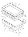
- FIG. 1 is an exploded perspective view showing a schematic configuration of a television receiver according to Embodiment 1 of the present invention.
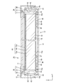
- the exploded perspective view which shows schematic structure of the liquid crystal display device with which a television receiver is equipped Sectional drawing which shows the cross-sectional structure along the short side direction of a liquid crystal display device
- the top view which shows the arrangement structure seen from the front side of the backlight apparatus
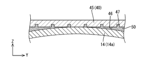
- Partial enlarged plan view of LED unit Schematic showing a cross-section of the contact surface between the LED unit and the chassis when the chassis has undulations
- the expanded sectional view of the LED unit and chassis which concern on the modification 1 of Embodiment 1.
- Partial enlarged plan view of LED unit The expanded sectional view of the LED unit and chassis which concern on the modification 2 of Embodiment 1.
- Partial enlarged plan view of LED unit The expanded sectional view of the LED unit which concerns on the modification 3 of Embodiment 1, and a chassis Partial enlarged plan view of LED unit The partial enlarged plan view of the LED unit which concerns on the modification 4 of Embodiment 1.
- FIG. The expanded sectional view of the LED unit and chassis concerning Embodiment 2
- FIG. 1 is an exploded perspective view showing a schematic configuration of a television receiver according to the present embodiment
- FIG. 2 is an exploded perspective view showing a schematic configuration of a liquid crystal display device 10
- FIG. 3 is along the short side direction of the liquid crystal display device 10.
- 4 is a plan view showing an arrangement configuration viewed from the front side of the backlight device 12
- FIG. 5 is a partially enlarged plan view of the LED unit 30,
- FIG. 6 is a case where undulation is present in the chassis 14.
- FIG. 2 is a schematic view showing a cross section of a contact surface between an LED unit 30 and a chassis 14.
- FIG. 2 Each drawing shows an X axis, a Y axis, and a Z axis, and the directions of the axes are drawn in the same direction in the drawings. Also, the upper side shown in FIG. 2 is the front side (front side, light emission side), and the lower side is the back side (back side, opposite to the light emission side).
- the television receiver TV includes a liquid crystal display device 10 (display device), front and back cabinets Ca and Cb that are accommodated so as to sandwich the liquid crystal display device 10, and a power source P.
- a tuner T and a stand S are provided.
- the liquid crystal display device 10 has a horizontally long rectangular shape (rectangular shape) as a whole and is accommodated in a vertically placed state.
- the liquid crystal display device 10 includes a liquid crystal panel 11 that is a display panel and a backlight device 12 (illumination device) that is an external light source, which are integrated by a frame-like bezel 13 or the like. Is supposed to be retained.
- the liquid crystal panel 11 has a rectangular shape in plan view, and a pair of glass substrates are bonded together with a predetermined gap therebetween, and liquid crystal is sealed between the glass substrates. It is said.
- One glass substrate is provided with a switching element (for example, TFT) connected to a source wiring and a gate wiring orthogonal to each other, a pixel electrode connected to the switching element, an alignment film, and the like.
- the substrate is provided with a color filter and counter electrodes in which colored portions such as R (red), G (green), and B (blue) are arranged in a predetermined arrangement, and an alignment film.
- a polarizing plate (not shown) is disposed outside both substrates.
- the driving of the liquid crystal panel 11 is controlled by a liquid crystal panel control unit (not shown).
- the liquid crystal panel control unit can output a control signal toward the liquid crystal panel 11 and control driving of the liquid crystal panel 11 based on an output signal output from an image signal processing unit (not shown).
- an image signal such as a television broadcast signal input to the tuner T via the antenna is input to the image signal processing unit.
- the input signal is subjected to image processing and the processed signal is processed. Output to a liquid crystal panel control unit or the like is possible.
- the backlight device 12 is disposed so as to cover a substantially box-shaped chassis 14 having an opening on the light emitting surface side (the liquid crystal panel 11 side), and the opening of the chassis 14.
- Optical member 15 group (diffusion sheet 15 a, lens sheet 15 b, reflective polarizing sheet 15 c), a frame disposed along the outer edge portion of the chassis 14 and holding the outer edge portion of the optical member 15 group sandwiched between the chassis 14 16.
- the backlight device 12 includes an LED unit 30 having LEDs 17 at both ends on the long side, and a so-called edge light type (side-light type) in which a light guide plate 18 is interposed between the LED units 30. Light type).
- edge light type side-light type
- Light type each component of the backlight device 12 will be described in detail.
- the chassis 14 is made of a metal such as an aluminum-based material, and has a rectangular bottom plate 14a similar to the liquid crystal panel 11 and a pair of the bottom plate 14a that rises from the outer end of the long side.
- the long side direction of the chassis 14 coincides with the X-axis direction (horizontal direction), and the short side direction coincides with the Y-axis direction (vertical direction).
- the bottom plate 14a is arranged in an opposing manner so as to cover the back side of the light guide plate 18 described later, that is, the surface opposite to the light emitting surface 18a.
- a power supply circuit board that supplies power to the liquid crystal panel 11 and the LED 17 and an LED control circuit board that controls driving of the LED are not shown on the back side of the bottom plate 14a of the chassis 14, that is, the back side of the backlight device 12.
- a liquid crystal control circuit board having the above-described liquid crystal panel control unit is attached.
- the optical member 15 has a rectangular shape in plan view, like the liquid crystal panel 11 and the chassis 14.
- the optical member 15 is configured by laminating a diffusion sheet 15a, a lens sheet 15b, and a reflective polarizing sheet 15c in this order from the light guide plate 18 side, and is disposed between the liquid crystal panel 11 and the light guide plate 18. Yes.
- Such an optical member 15 has a function of converting light emitted from the LED 17 and passing through the light guide plate 18 into planar light.
- the frame 16 arranged on the optical member 15 has a frame shape like the bezel 13 and is fixed to the long side of the chassis 14 and receives the outer peripheral edge of the liquid crystal panel 11 from the back side. It is supposed to be possible.
- the light guide plate 18 is made of a synthetic resin material (for example, acrylic) having a refractive index sufficiently higher than air and substantially transparent (exceeding translucency), has a rectangular shape in plan view, and has a predetermined thickness. It is formed in a plate shape. As shown in FIG. 2, the light guide plate 18 is disposed in the chassis 14 immediately below the liquid crystal panel 11 and the optical member 15, and is sandwiched between a pair of LED units 30 disposed at both ends in the long side direction of the chassis 14. It is arranged in a form. Specifically, the main plate surface of the light guide plate 18 is directed to the front side (optical member 15 side), and is arranged along the display surface of the liquid crystal panel 11 in parallel.
- a synthetic resin material for example, acrylic
- the light guide plate 18 is disposed in the chassis 14 immediately below the liquid crystal panel 11 and the optical member 15, and is sandwiched between a pair of LED units 30 disposed at both ends in the long side direction of the chassis 14. It is arranged in a form. Specifically, the
- both side surfaces on the long side disposed facing the LED 17 are light incident surfaces 18 a on which light from the LED 17 is incident.
- the main plate surface arranged on the front side (optical member 15 side) of the light guide plate 18 is a light emitting surface 18b that emits light from the LED 17 (see FIGS. 2 and 3).
- the light guide plate 18 introduces light emitted from the LED 17 in the Y-axis direction from the light incident surface 18a and directs the light toward the optical member 15 side (Z-axis direction) while propagating the light inside. And has a function of emitting from the light exit surface 18b.
- the reflection sheet 19 is made of synthetic resin (for example, made of foamed PET), and its surface is white with excellent light reflectivity.
- the reflection sheet 19 is disposed so as to cover the entire back surface of the light guide plate 18, that is, the surface opposite to the light emitting surface 18b.
- the reflection sheet 19 allows the light in the light guide plate 18 to be reflected and raised to the light exit surface 18b side.
- the LED unit 30 includes an LED 17, a main board 31 on which the LED 17 is mounted, and a heat dissipation plate 40 that fixes the main board 31. 2 to 4, the LED 17 is fixed on the main substrate 31 constituting the LED unit 30 and the LED chip is sealed with a resin material.
- the LED chip mounted on the mounting surface 32 of the main substrate 31 has a single main emission wavelength, and specifically, one that emits blue in a single color.
- the resin material that seals the LED chip is dispersed and blended with a phosphor that emits a predetermined color when excited by the blue light emitted from the LED chip, and generally emits white light as a whole. It is said.
- the phosphor for example, a yellow phosphor that emits yellow light, a green phosphor that emits green light, and a red phosphor that emits red light are used in appropriate combination, or any one of them is used. It can be used alone. As a result, the LED 17 can emit white light.
- the LED 17 is a so-called top type in which a surface opposite to the mounting surface 32 to be mounted is a light emitting surface.
- the main board 31 on which the LED 17 is mounted has an elongated plate shape extending along the long side plate 14 b of the chassis 14, and the main board surface extends in the X axis direction and the Z axis. It is accommodated in the chassis 14 in a posture parallel to the direction, that is, a posture orthogonal to the plate surfaces of the liquid crystal panel 11 and the optical member 15.
- a pair of main substrates 31 are arranged corresponding to both ends on the long side in the chassis 14, that is, arranged so as to face the light incident surfaces 18 a that are both side surfaces on the long side of the light guide plate 18. Become.
- the main substrate 31 has a mounting surface 32 that faces the light incident surface 18 a of the light guide plate 18, and the LEDs 17 are surface-mounted on the mounting surface 32.
- a plurality of LEDs 17 are intermittently arranged in parallel along the longitudinal direction (X-axis direction) on the mounting surface 32.
- the base material of the main board 31 is made of the same metal as the chassis 14 such as an aluminum-based material.
- the mounting surface 32 has an insulating layer formed by applying an insulating material, and an insulating layer on the insulating layer. And patterned circuit wiring.
- the circuit wiring is made of a metal film such as copper foil, and adjacent LEDs 17 are connected in series by this circuit wiring.
- the heat radiating plate 40 is made of a metal such as the same aluminum material as the chassis 14, and the overall shape thereof is in the long side direction (X-axis direction) of the chassis 14 (light guide plate 18) as shown in FIGS. 2 to 4.
- the elongated thin flat plate is bent so as to have an L-shaped cross section.
- a portion disposed along the long side plate 14 b of the chassis 14 is a board mounting portion 41
- a portion disposed along the bottom plate 14 a of the chassis 14 is a heat radiating portion 45. That is, the board mounting portion 41 is configured to rise substantially vertically from the end of the heat radiating portion 45 to the front side.
- the substrate mounting portion 41 is parallel to the light incident surface 18a of the light guide plate 18 and faces the light incident surface 18a.
- the substrate mounting portion 42 is a substrate mounting surface 42 to which the main substrate 31 is mounted, and the opposite surface, which is a chassis. 14 and a chassis attachment surface 43 attached in contact with the inner surface of the long side plate 14b.
- the entire surface opposite to the mounting surface 32 of the main substrate 31 is attached to the substrate mounting surface 42 in close contact with the light mounting surface 18a of the light guide plate 18 and the main substrate 31. The distance from the LED 17 is kept constant.
- the heat radiation part 45 is configured to extend along the bottom plate 14 a in parallel with the bottom plate 14 a of the chassis 14, and the extending direction is a direction from the substrate mounting part 41 toward the light guide plate 18.
- the extending edge of the heat radiating portion 45 has an extending length that exceeds the light incident surface 18 a of the light guide plate 18, that is, is arranged so as to partially overlap the light guide plate 18.
- the extending length of the heat dissipating part 45 is longer than the length of the board mounting part 41 in the Z-axis direction, and ensures a wider contact area with the bottom plate 14a of the chassis 14.
- the heat radiation portion 45 has a heat radiation surface 46 facing the bottom plate 14a of the chassis 14.
- the heat radiating surface 46 has a groove 47 extending linearly along the long side direction thereof, that is, the long side direction (X-axis direction) of the chassis 14 and along the parallel direction of the LEDs 17.
- a plurality of recesses are provided.
- the grooves 47 are parallel to each other, and the cross section in the Y-axis direction is rectangular. Both ends of each groove 47 are open ends 48 that reach both ends in the long side direction of the heat radiating surface 46, that is, each groove 47 is configured to penetrate the heat radiating surface 46 in the long side direction.
- the depth of the groove 47 from the surface of the heat radiating surface 46 is preferably about 1 mm to 5 mm.
- the heat radiating surface 46 in which the groove 47 is formed is fixed with screws or the like so as to contact the bottom plate 14a over the entire surface. And the clearance gap between the groove
- the heat radiating material 50 may be at least a heat conductive material that is in a liquid state at the time of filling.
- a liquid silicone material before polymerization as silicone rubber is used.
- the silicone material a thermosetting type that cures (polymerizes) by heating, a room temperature curing type that absorbs moisture in the air and cures, a photocuring type that cures by UV irradiation, and the like can be selected as appropriate.
- both members are in contact with each other and a slight gap is filled with the heat radiating material 50. That is, the entire surface of the heat radiating surface 46 is in contact with the bottom plate 14 a of the chassis 14 facing directly or through the heat radiating material 50. Therefore, the heat generated from the LED 17 is conducted from the main board 31 to the heat radiating plate 40, and is conducted from the heat radiating surface 46 of the heat radiating portion 45 directly or through the heat radiating material 50 to the bottom plate 14 a of the chassis 14. Heat is radiated to the external space. There is also a route in which heat is transferred from the chassis mounting surface 43 of the board mounting portion 41 to the long side plate 14b of the chassis 14 and radiated to the external space.
- the liquid crystal display device 10 having the above-described configuration is manufactured by assembling a separately manufactured liquid crystal panel 11 and backlight device 12 with a bezel 13 or the like.
- the LED unit 30 which is a component of the backlight device 12 is housed in the chassis 14 when assembled, as shown in FIG. Specifically, screws or the like are used so that the chassis mounting surface 43 of the board mounting portion 41 of the heat radiating plate 40 contacts the long side plate 14b, and the heat radiating surface 46 of the heat radiating portion 45 contacts the bottom plate 14a. To fix.
- the heat radiating material 50 is injected into the groove 47 by injecting the heat radiating material 50 from the open ends 48 of the grooves 47 opened at both ends in the long side direction of the heat radiating plate 40. Filled. At this time, if there are irregularities or undulations on the surface of the bottom plate 14a of the chassis 14 facing the heat radiating surface 46 of the heat radiating plate 40, the heat radiating material 50 injected into the groove 47 as shown in FIG. By flowing out into the gap, the heat radiation material 50 is also filled in the gap between the heat radiation surface 46 and the bottom plate 14a of the chassis 14.
- the heat radiating surface 46 is in direct contact with the bottom plate 14a of the chassis 14 without a gap or in contact with the heat radiating member 50. As will be described in detail later, the heat generated from the LED 17 is generated by the heat radiating plate 40. Heat is transferred to the bottom plate 14 a of the chassis 14 through the entire heat radiating surface 46.
- the drive of the liquid crystal panel 11 is controlled by a liquid crystal panel control unit (not shown), and the drive of each LED 17 in the backlight device 12 is controlled by the LED control circuit board.
- illumination light is applied to the liquid crystal panel 11, and a predetermined image is displayed on the liquid crystal panel 11.
- each LED 17 is turned on, the light emitted from each LED 17 enters the light incident surface 18 a of the light guide plate 18.
- the light taken in from the light incident surface 18a propagates through the light guide plate 18 by being reflected by the reflection sheet 19, and is emitted as substantially planar light from the light emitting surface 18b.
- the heat radiation action in the LED unit 30 will be described.
- the heat generated from each LED 17 is transferred from the main board 31 to the heat radiating plate 40 through the board mounting surface 42.
- the heat conducted to the heat radiating plate 40 is transferred from the chassis mounting surface 43 to the long side plate 14 b of the chassis 14.
- heat is transferred from the heat radiation surface 46 of the heat radiation portion 45 to the bottom plate 14 a of the chassis 14.
- the heat conducted to the chassis 14 is radiated to an external space outside the liquid crystal display device 10.
- it is set as the structure excellent in the heat dissipation effect by ensuring the contact area to the chassis 14 used as the heat medium of LED unit 30 with which LED17 which is a heat source was mounted.
- a plurality of grooves 47 are formed in the heat dissipation surface 46 having the largest area, and at least the grooves 47 are filled with the heat dissipation material 50. ing. If the surface of the chassis 14 has irregularities or undulations, the heat radiation material 50 is also filled in the gap formed between the heat radiation surface 46 and the chassis 14 due to the surface shape in addition to the grooves 47. (See FIG. 6). With this heat radiating material 50, the heat radiating surface 46 can transfer heat over the entire surface of the bottom plate 14 a of the chassis 14, so that the heat radiating efficiency can be improved.
- the efficiency is inferior to the theoretical heat radiating efficiency in which the entire heat radiating surface 46 is in close contact with the chassis 14 due to this gap.
- a heat insulation effect is generated by sandwiching air in the gap between the heat dissipation surface 46 and the chassis 14, and This is because the heat transfer efficiency is lowered.
- a plurality of grooves 47 are provided in the heat dissipation surface 46 having the widest contact area, and the surface area is increased.
- the heat transfer surface 46 can be used directly or via the heat dissipation material 50 as a path for transferring heat to the bottom plate 14a. Therefore, the heat dissipation efficiency can be improved. Further, by filling the heat dissipation material 50 in the groove 47 and the gap between the chassis 14 and the LED unit 30, a contact area can be ensured and a stable thermal design can be performed.
- the backlight device 12 of the present embodiment includes the LED 17, the LED unit 30 on which the LED 17 is mounted, the light incident surface 18a that faces the LED 17 and the light from the LED 17 is incident thereon, and the light.
- the LED unit 30 and the chassis 14 are disposed between the LED unit 30 and the chassis 14. It is intimately contacted by filling the liquid heat dissipation material 50.
- the liquid heat radiation material 50 is filled between the heat radiation surface 46 of the heat radiation plate 40 and the bottom plate 14 a of the chassis 14. Regardless of the surface shape of the bottom plate 14a, the heat radiation surface 46 and the bottom plate 14a of the chassis 14 can be brought into close contact with each other, and the heat radiation efficiency for radiating the heat from the LED 17 to the external space through the chassis 14 can be improved. It is.
- a groove 47 is formed in the heat dissipation surface 46 on the LED unit 30 side, and at least the groove 47 is filled with the heat dissipation material 50.
- the surface area of the heat radiating surface 46 can be increased by forming the groove 47, and heat can be transferred to the bottom plate 14a of the chassis 14 via the heat radiating member 50 without leaving the increased surface area. By doing so, the heat dissipation efficiency can be further improved.
- the LED unit 30 includes a main board 31 on which the LEDs 17 are mounted, and a heat radiating plate 40 that is fixed to the chassis 14 by fixing the main board 31 so that heat can be transferred.
- the main board 31 is a flat plate on which the LED 17 can be easily mounted, and the heat radiating plate 40 has a shape that ensures a large contact surface with the chassis 14 (in this embodiment, the chassis mounting surface 43 and the heat radiating surface 46). it can.
- both ends of the groove 47 are open ends 48 that reach both ends in the long side direction of the heat radiating surface 46 in which the groove 47 is formed, and the heat radiating material in a state in which the groove 47 is blocked by the bottom plate 14a of the chassis 14 facing the groove 47. 50 can be injected from the open end 48. With such a configuration, since the heat dissipation material 50 can be injected and filled from the open end 48 after the LED unit 30 is attached to the chassis 14, the workability is excellent. Further, since the groove 47 is linear, it is easy to fill the heat dissipation material 50.
- the groove 47 is formed in the heat radiating surface 46 of the LED unit 30. Since the LED unit 30 is smaller than the chassis 14, it is easier to form the LED unit 30 than to form the groove 47 in the bottom plate 14 a of the chassis 14.
- the heat radiating plate 40 includes a heat radiating portion 45 facing the chassis 14 and a substrate mounting portion 41 that can be raised from one end of the heat radiating portion 45 and to which the main substrate 31 can be attached, and has a substantially L shape in sectional view.
- chassis 14, the heat sink 40, and the main board 31 are all made of a metal such as an aluminum material and are made of the same material. As described above, if the same material is used in the heat transfer path between the LED 17 and the chassis 14, the thermal resistance can be suppressed and the heat radiation efficiency can be improved. Moreover, by making it metal, it shall be excellent in thermal conductivity and the improvement of the thermal radiation efficiency can be anticipated further.
- the light guide plate 18 has a flat plate shape, the plate surface is a light emitting surface 18b, and the side surface facing the LED 17 is a light incident surface 18a.
- the chassis 14 is arranged in parallel to the light emitting surface 18b.
- a long side plate 14b that rises from the periphery of the bottom plate 14a and is arranged in parallel to the light incident surface 18a.
- the LEDs 17 are mounted on the main board 31 with a high density in order to obtain a necessary light amount, and the amount of heat generated per unit area on the main board 31 tends to increase. Therefore, it is particularly useful to apply a configuration in which the chassis 14 and the LED unit 30 of the present embodiment are in close contact with each other by filling the heat dissipation material 50.
- the LED 17 as the light source, it is possible to extend the life of the light source and reduce power consumption.
- the heat dissipation material 50 is excellent in handling because it can be treated as a solid when discarded by using a material that is hardened after being filled in a liquid state. Moreover, if it is the sclerosing
- the heat dissipation material 50 is preferably silicone rubber. If a liquid silicone material having a high curing rate is used, the time required for curing can be shortened and the manufacturing cost can be reduced.
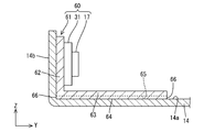
- FIG. 7 is an enlarged cross-sectional view of the LED unit 60 and the chassis 14 according to this modification
- FIG. 8 is an enlarged plan view of the LED unit 60.
- the LED unit 60 includes a main board 31 on which the LEDs 17 are mounted, and a heat radiating plate 61 that attaches the main board 31 to the board mounting portion 62.
- the heat radiating plate 61 is formed by bending an elongated flat plate extending in the long side direction (X-axis direction) of the chassis 14 so as to have an L-shaped cross section.
- the board attaching part 62 which faces the inner surface of 14b, and the thermal radiation part 63 distribute
- the surface of the heat radiating portion 63 that faces the bottom plate 14 a of the chassis 14 is a heat radiating surface 64, and a plurality of grooves 65 are formed in the heat radiating surface 64.
- Each groove 65 is recessed in the heat radiation surface 64 so as to form a straight line extending in the short side direction (Y-axis direction) of the chassis 14, that is, in the direction orthogonal to the parallel direction of the LEDs 17.
- the grooves 65 are parallel to each other, and the cross section in the X-axis direction is rectangular. Both ends of each groove 65 are open ends 66 that reach both ends of the heat radiating surface 64 in the short side direction, that is, each groove 65 is configured to penetrate the heat radiating surface 64 in the short side direction.
- a liquid heat dissipating material (not shown) is assumed to be the same as in the first embodiment. Inject from open end 66. At this time, the open end 66 opened on the board mounting portion 62 is in a state of being blocked by the long side plate 14b of the chassis 14 that abuts. Therefore, if the heat radiating material is injected from the other open end 66, the injected heat radiating material can be filled in the groove 65 without leaking.
- the two may not be in close contact with each other and a gap may be formed.
- the heat radiating material injected into the groove 65 flows into the gap, so that the heat radiating material is filled with no gap between the two members.
- the heat radiating surface 64 of the heat radiating plate 61 of the LED unit 60 it is possible to secure a larger contact area of the heat radiating surface 64 of the heat radiating plate 61 of the LED unit 60 with the bottom plate 14a of the chassis 14, so that the heat radiating efficiency is improved.
- a plurality of grooves 65 are formed in the heat radiation surface 64, and the heat radiation material is filled by filling the gaps formed in the grooves 65 and between the heat radiation surface 64 and the bottom plate 14a of the chassis 14 so that the heat radiation. Since the surface 64 can conduct heat over the entire surface of the bottom plate 14a of the chassis 14, the heat radiation efficiency can be improved. Further, by increasing the surface area by forming the groove 65 in the heat radiating surface 64, it is possible to expect an improvement in heat radiating efficiency by ensuring a large surface area for radiating heat.
- one end of the open end 66 of the groove 65 is the length of the chassis 14 when the extending direction of the groove 65 is the short side direction (Y-axis direction) of the chassis 14. It will be blocked by the side plate 14b. Thereby, the heat radiating material injected from the other open end 66 can be filled without leaking from the other open end 66. Further, since the extension length of each groove 65 is shorter than that of the first embodiment, it is possible to fill the groove 65 with the heat dissipation material evenly without increasing the injection pressure when injecting the heat dissipation material. .
- FIG. 9 is an enlarged cross-sectional view of the LED unit 70 and the chassis 14 according to this modification
- FIG. 10 is an enlarged plan view of the LED unit 70.
- the LED unit 70 includes a main board 31 on which the LEDs 17 are mounted, and a heat radiating plate 71 in which the main board 31 is attached to the board attaching portion 72.
- the heat radiating plate 71 is formed by bending an elongated flat plate extending in the long side direction (X-axis direction) of the chassis 14 so as to have an L-shaped cross section.
- a board mounting portion 72 facing the inner surface of the long side plate 14b of the chassis 14 and a heat radiating portion 73 disposed along the bottom plate 14a of the chassis 14 are provided.
- a surface of the heat radiating portion 73 facing the bottom plate 14 a of the chassis 14 is a heat radiating surface 74, and a groove 75 is formed in the heat radiating surface 74.
- the grooves 75 are formed in a lattice shape on the heat dissipation surface 74. Specifically, linear grooves extending along the long side direction (X-axis direction) of the chassis 14 are formed in parallel at predetermined intervals, and the short side direction (Y-axis direction) of the chassis 14 is formed. Are formed in parallel with each other at predetermined intervals, and the grooves extending in the X-axis direction and the grooves extending in the Y-axis direction intersect to form a lattice-like groove 75. ing.
- the groove 75 has a square cross section, and the end of the groove 75 reaches the outer edge of the heat radiating surface 74, that is, both ends in the short side direction and both ends in the long side direction of the heat radiating surface 74.
- the open end 76 is open to the front.
- the liquid heat radiating material 77 (same as in the first embodiment) is used as the open end of the groove 75. Inject from 76. At this time, the open end 76 opened on the board mounting portion 72 is closed by the long side plate 14b of the chassis 14 that abuts, but the other open end 76 opened to the other is open. Therefore, from which open end 76 the heat radiating material 77 is injected at the same time from each open end 76, or selected from a plurality of open ends 76 and the heat radiating material 77 is injected, it can be appropriately selected. Yes.
- the heat radiating material 77 injected into the groove 75 flows into the gap, so that the heat radiating material 77 is filled with no gap between the two members.
- the contact area of the heat dissipation surface 74 of the heat dissipation plate 71 of the LED unit 70 with the bottom plate 14a of the chassis 14 can be ensured as in the first embodiment and the first modification of the first embodiment.
- the heat radiation efficiency can be improved. That is, a grid-like groove 75 is formed in the heat radiating surface 74, and the heat radiating material 77 is filled in the gap 75 formed between the groove 75 and the heat radiating surface 74 and the bottom plate 14 a of the chassis 14. Since the heat radiating surface 74 can transfer heat to the bottom plate 14a of the chassis 14 over the entire surface, the heat radiating efficiency can be improved. Further, by increasing the surface area by forming the groove 75 in the heat radiating surface 74, it is possible to expect improvement in heat radiating efficiency by ensuring a large surface area for radiating heat.
- the grooves 75 are not formed in one direction as in the first embodiment or the first modification of the first embodiment, but are formed in a lattice shape so as to intersect the two directions, thereby forming the grooves 75. Not only can the surface area of the heat dissipation surface 74 be increased, but also more heat dissipation material 77 can be filled.
- the heat radiating material 77 injected into the groove 75 is similarly formed in the gap.
- the gap is filled by flowing out.
- the grooves 75 are formed in a lattice shape as in the present modification, the grooves 75 are arranged closer to each gap, so that the heat radiating material 77 passes through the grooves 75. Easy to fill inside. In other words, it is easy to avoid a situation in which the gap between the chassis 14 and the heat radiation surface 74 is not filled with the heat radiation material 77. Therefore, the heat radiation material 77 is more evenly filled in the groove 75 and the gap between the chassis 14 and the heat radiation surface 74, so that the heat radiation efficiency in the heat transfer path via the heat radiation material 77 can be improved.
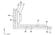
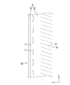
- FIG. 11 is an enlarged cross-sectional view of the LED unit 80 and the chassis 14 according to this modification
- FIG. 12 is an enlarged plan view of the LED unit 80.
- the LED unit 80 includes a main board 31 on which the LEDs 17 are mounted, and a heat radiating plate 81 that attaches the main board 31 to the board mounting portion 82.
- the heat radiating plate 81 is formed by bending an elongated flat plate extending in the long side direction (X-axis direction) of the chassis 14 so as to have an L-shaped cross section.
- the board attaching part 82 which faces the inner surface of the long side plate 14b of the chassis 14 and the heat radiating part 83 arranged along the bottom plate 14a of the chassis 14 are provided.
- the surface of the heat radiating portion 83 that faces the bottom plate 14 a of the chassis 14 is a heat radiating surface 84, and a plurality of grooves 85 are formed in the heat radiating surface 84.
- Each groove 85 extends along the Y-axis direction from the long side on the chassis 14 center side toward the long side plate 14 b on the outer edge of the heat radiating surface 84, and the tip thereof is at the substantially central portion in the short side direction of the heat radiating surface 84. Has reached.
- the grooves 85 are parallel to each other, and the cross section in the X-axis direction is rectangular.
- the edge that opens toward the center of the chassis 14 is an open end 86, that is, only one end of the groove 85 reaches the outer edge of the heat dissipation surface 84.
- a liquid heat radiating material (not shown) is assumed to be the same as in the first embodiment. Inject from the open end 86. At this time, since there is one open end 86 for each groove 85, it is possible to fill the groove 85 with the heat radiating material without the heat radiating material filled from the open end 86 leaking out. Moreover, between the bottom plate 14a of the chassis 14 and the heat radiating surface 84, if there are uneven shapes or undulations on the mutual contact surfaces, they may not be in close contact with each other and a gap may be formed. In this case, the heat radiating material injected into the groove 85 flows into the gap, so that the heat radiating material is filled with no gap between the two members.
- the surface area is increased by forming the groove 85 on the heat radiating surface 84 and the heat radiating member is formed in the groove 85 and the same as in the first and second modifications of the first embodiment and the first embodiment.
- channel 85 in the thermal radiation surface 84 is not made into the open end 86, but the possibility that the thermal radiation material to inject
- the region close to the light guide plate 18 not only transfers heat from the LED 17 through the main substrate 31, but also absorbs heat from the atmosphere that has been heated by the light source light emitted from the LED 17. Therefore, it is necessary to increase the heat radiation efficiency compared to other parts. By disposing the groove 85 and the heat radiating material in this region, it is possible to improve the heat radiating efficiency while reducing the use amount of the heat radiating material and reducing the cost.
- FIG. 13 is an enlarged plan view of an LED unit 90 according to this modification.
- the LED unit 90 includes a main board 31 on which the LEDs 17 are mounted and a heat radiating plate 91 to which the main board 31 is attached.
- the heat radiating plate 91 includes a board mounting portion 92 facing the inner surface of the long side plate 14 b of the chassis 14, and a heat radiating portion 93 disposed along the bottom plate 14 a of the chassis 14.
- a surface of the heat radiating portion 93 that faces the bottom plate 14a of the chassis 14 is a heat radiating surface, and a plurality of grooves 94 are formed on the heat radiating surface.
- Each groove 94 extends from the long side of the outer side of the heat radiating surface toward the long side plate 14b toward the long side plate 14b with a slight inclination in the X-axis direction. Has reached the department.
- the grooves 94 are parallel to each other, and an edge that opens toward the center of the chassis 14 is an open end 95.
- the groove 94 is formed on the heat radiating surface to increase the surface area, and the heat radiating material is formed on the groove 94 and the heat radiating surface. And filling the gap between the bottom plate 14a of the chassis 14 facing the heat dissipation efficiency in the heat transfer path for dissipating the heat from the LED 17 to the external space.
- FIG. 14 is an enlarged cross-sectional view of the LED unit 100 and the chassis 14 according to the present embodiment.
- the shape of the heat radiating plate 101 is a mode in which an elongated flat plate extending in the long side direction (X-axis direction) of the chassis 14 is bent so as to have an L-shaped cross section, and the main board on which the LEDs 17 are mounted.
- the board attaching part 102 to which 31 is fixed and the heat radiating part 103 in contact with the bottom plate 14a of the chassis 14 are formed.
- the extending direction of the heat dissipating part 103 with respect to the substrate mounting part 102 extends to the long side plate 14b side, that is, the side opposite to the light guide plate 18.
- the surface of the heat radiating portion 103 facing the bottom plate 14a of the chassis 14 is a heat radiating surface 104.
- a plurality of linear grooves 105 are provided in the heat radiating surface 104 as in the first embodiment.
- the extending direction of each groove 105 is the long side direction (X-axis direction) of the chassis 14 and is parallel to each other. Both ends of each groove 105 reach both ends in the long side direction of the heat radiating surface 104, that is, each groove 105 is configured to penetrate the heat radiating surface 104 in the short side direction.
- a heat radiating material 106 is injected into each groove 105, and a gap formed between the groove 105 and the bottom plate 14 a of the chassis 14 facing the heat radiating surface 104 is filled with the heat radiating material 106.
- the heat radiating part 103 is arranged on the outer peripheral edge side of the chassis 14 on the opposite side of the light guide plate 18 with respect to the board mounting part 102, the heat radiating efficiency can be further improved.
- the heat dissipating part 103 when the heat dissipating part 103 is disposed on the light guide plate 18 side with respect to the substrate mounting part 102 and covers the region for mixing the light source light from the LED 17 to the light incident surface 18a of the light guide plate 18, the heat dissipating part 103 is the main substrate.
- the heat is absorbed not only from the heat transfer from 31 but also from the atmosphere that is higher in temperature than the other parts by the light source light, and the heat radiation efficiency of the heat radiation unit 103 is lowered.
- the heat radiation efficiency can be improved by arranging the heat radiation part 103 on the outer peripheral edge side of the chassis 14 having a low ambient temperature.
- the heat radiating part 103 is arranged on the light guide plate 18 side with respect to the substrate mounting part 102, there is a possibility that a part of the light guide plate 18 and the heat radiating part 103 overlap to increase the thickness of the backlight device 12. is there.
- the heat radiating portion 103 is formed on the opposite side of the light guide plate 18 with respect to the substrate mounting portion 102, the backlight device 12 is made thinner, and the heat radiating efficiency is further improved. be able to.
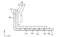
- FIG. 15 is an enlarged cross-sectional view of the LED unit 110 and the chassis 14 according to the present embodiment.
- the LED unit 110 includes a main board 31 on which the LEDs 17 are mounted, and a heat sink 111 that fixes the main board 31 to the board mounting portion 112.
- the heat radiating plate 111 is formed by bending an elongated flat plate extending in the long side direction (X-axis direction) of the chassis 14 so as to have an L-shaped cross section.
- arranged along the bottom plate 14a of the chassis 14 are provided.
- a surface of the heat radiating portion 113 facing the bottom plate 14 a of the chassis 14 is a heat radiating surface 114.
- a plurality of linear grooves 115 are formed in a portion of the bottom plate 14 a of the chassis 14 that faces the heat radiating surface 114. Each groove 115 extends along the long side plate 14b of the chassis 14 and is parallel to each other. The groove 115 is filled with a heat dissipation material 116 (similar to the first embodiment).
- the present invention is not limited to forming the groove 115 on the LED unit 110 side and filling the heat dissipation material, but forming the groove 115 on the chassis 14 side and filling the groove 115 with the heat dissipation material 116.
- the effect of can be obtained. That is, when the heat dissipation surface 114 and the surface of the bottom plate 14a of the chassis 14 opposite to the heat dissipation surface 114 have uneven shapes and undulations, the entire heat dissipation surface 114 cannot be brought into close contact with the chassis 14, and the heat is released by the amount of the gap. There is a risk that the efficiency may decrease.
- the groove 115 is formed in the bottom plate 14a of the chassis 14 facing the heat radiating surface 114, and the heat radiating material 116 is filled therein, so that at least the heat radiating material 116 has the heat radiating surface 114 and the inner surface of the groove 115 of the chassis 14. Therefore, a heat transfer path through the heat dissipating material 116 can be established.
- heat dissipation efficiency can be improved.
- stable thermal design is possible.
- FIG. 16 is an enlarged cross-sectional view of the LED unit 120 and the chassis 14 according to the present embodiment.
- the LED unit 120 includes an LED 17 and a heat radiating plate 121 on which the LED 17 is mounted and fixed to the chassis 14.
- the shape of the heat sink 121 is a mode in which an elongated flat plate extending in the long side direction (X-axis direction) of the chassis 14 is bent so as to have an L-shaped cross section.
- a mounting portion 122 facing the inner surface of the side plate 14b and a heat radiating portion 123 disposed along the bottom plate 14a of the chassis 14 are provided.
- a surface of the heat radiating portion 123 that faces the bottom plate 14 a of the chassis 14 is a heat radiating surface 124.
- a plurality of linear grooves 125 are formed on the heat radiating surface 124, and the grooves 125 extend in the long side direction (X-axis direction) of the chassis 14 and are parallel to each other. Both ends of each groove 125 reach both ends in the long side direction of the heat radiating surface 124, that is, each groove 125 is configured to penetrate the heat radiating surface 124 in the long side direction.
- the gaps formed in the grooves 125 and between the heat sink surface 124 and the bottom plate 14a of the chassis 14 facing each other are filled with a heat dissipation material 126.
- the mounting part 122 has a mounting surface 122a facing the light incident surface 18a of the light guide plate 18, and the LED 17 is surface-mounted on the mounting surface 122a.
- the mounting form is the same as the mounting form of the LED 17 on the main board 31 of the first embodiment.
- the mounting surface 122a has an insulating layer formed by applying an insulating material, and an insulating layer on the insulating layer. Patterned circuit wiring is arranged.
- the circuit wiring is made of a metal film such as copper foil, and adjacent LEDs 17 are connected in series by this circuit wiring.
- the heat radiating surface 124 is provided with a plurality of grooves 125, and a heat radiating material 126 is filled in the gap 125 and between the heat radiating surface 124 and the bottom plate 14 a of the chassis 14 facing the heat radiating surface 124.
- the heat dissipation surface 124 can be used as a heat transfer path that leads to the chassis 14 without leaving any excess, and the heat dissipation efficiency can be further improved. Further, by eliminating the main substrate 31, it is possible to save space, which is advantageous in reducing the size of the backlight device 12, particularly the narrow frame around the light guide plate 18.
- the present invention is not limited to the above-described embodiment, and for example, the following modifications may be included.
- the same members as those in the above embodiment are denoted by the same reference numerals as those in the above embodiment, and description thereof may be omitted.
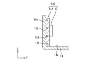
- FIG. 17 is an enlarged cross-sectional view of the LED unit 130 and the chassis 14 according to the present embodiment.
- the LED unit 130 includes an LED 17 and a heat radiating plate 131 on which the LED 17 is mounted and fixed to the chassis 14.
- the shape of the heat radiating plate 131 is an elongated flat plate extending in the long side direction (X-axis direction) of the chassis 14, and the mounting surface 132 facing the light incident surface 18 a of the light guide plate 18, and It is provided with a heat radiating surface 133 which is the opposite surface and faces the long side plate 14 b of the chassis 14.
- the LED 17 is surface-mounted on the mounting surface 132.
- the mounting form is the same as that of the fourth embodiment.
- a plurality of linear grooves 134 are formed on the heat radiation surface 133, and each groove 134 extends in the long side direction (X-axis direction) of the chassis 14 and is parallel to each other. Both ends of each groove 134 reach both ends in the long side direction of the heat radiating surface 133, that is, each groove 134 is configured to penetrate the heat radiating surface 133 in the long side direction.
- the main board 31 is not interposed.
- the number of interfaces can be reduced to reduce the thermal resistance, thereby improving the heat dissipation efficiency.
- space-saving can be achieved by using a flat plate shape instead of the heat radiating plate 131 bent in an L-shaped cross section as in the first to fourth embodiments. That is, although the contact area of the heat sink 131 with respect to the chassis 14 is reduced as compared with the first to fourth embodiments, a part of the heat radiating portion 45 does not overlap the light guide plate 18 as in the first embodiment.
- the backlight device 12 can be thinned.
- the heat radiating surface 133 is provided with a plurality of grooves 134, and a heat radiating material 135 is formed in the gap formed between the groove 134 and the long side plate 14 b of the chassis 14 facing the heat radiating surface 133. Therefore, even if the contact area with respect to the chassis 14 is reduced, it can be expected to improve the heat dissipation efficiency.
- silicone rubber is exemplified as the heat radiating material.
- the present invention is not limited to this, and any heat conductive material that is liquid at the time of filling may be used. It may be a material that can be cured or a material that cures over time. Moreover, it is not limited to filling, and a heat radiating material that maintains a liquid state may be used, or a material that is liquid at room temperature and is cured by a temperature increase caused by lighting of the LED 17 may be used.
- the groove formed in the heat radiating surface or the chassis 14 has a depth direction perpendicular to the forming surface.
- the groove may be cut obliquely.
- the heat dissipation material is injected from the open end of the groove.
- the present invention is not limited to this.
- the heat dissipation material is previously injected into the groove. It may be cured. With such a configuration, it is possible to assemble in the same assembling process as before, so that no special change occurs and the versatility can be improved.
- a groove is formed as a recess, and the groove is exemplified as a linear or grid-like one.
- the present invention is not limited to this.
- a single recess having a square shape or a circular shape is provided. It may be formed, or a so-called zigzag-shaped recess having continuous peaks and valleys may be formed.
- the substrate holding part and the heat radiating part of the heat radiating plate are exemplified in which the surface area of the heat radiating part is larger than the surface area of the substrate holding part.
- the substrate holding unit and the heat radiating unit may have substantially the same surface area, or the substrate holding unit may have a surface area larger than that of the heat radiating unit.
- the recess (groove) is provided only in the heat radiating portion.
- the present invention is not limited to this.
- the heat radiating portion not only the heat radiating portion but also the substrate holding portion or the mounting portion is mounted with the LED 17.
- a configuration may also be adopted in which a concave portion is formed on the surface opposite to the surface on which the heat sink is provided and the heat dissipation material is filled.
- a configuration may be employed in which a recess is formed in only the substrate holding portion or the mounting portion and the heat dissipation material is filled without forming the recess in the heat dissipation portion.
- the LED units are disposed at both ends on the long side of the backlight device 12.
- the present invention is not limited to this, and either one of the long sides of the backlight device 12 is used.
- the LED unit is disposed on the both ends of the short side, or the LED unit is disposed on either one of the both sides.
- the edge light type backlight device 12 using the LED 17 as the light source is adopted.
- the present invention is not limited to this.
- the edge light type backlight device 12 using a linear light source such as a discharge tube is used.
- a backlight device may be employed.
- the LED 17 including the LED chip that emits blue monochromatic light is used.
- an LED including the LED chip that emits purple monochromatic light is used.
- an LED incorporating three types of LED chips each emitting R, G, and B in a single color is also possible.
- the TFT is used as the switching element of the liquid crystal display device 10, but the present invention can also be applied to a liquid crystal display device using a switching element other than the TFT (for example, a thin film diode (TFD)).
- a switching element other than the TFT for example, a thin film diode (TFD)
- the present invention can also be applied to a liquid crystal display device for monochrome display.
- liquid crystal display device 10 using the liquid crystal panel 11 as the display panel has been illustrated, but the present invention can also be applied to display devices using other types of display panels.
- the television receiver 10 including the tuner T is illustrated, but the present invention can also be applied to a display device that does not include the tuner.
- SYMBOLS 10 Liquid crystal display device (display device), 11 ... Liquid crystal panel (display panel), 12 ... Backlight device (illumination device), 14 ... Chassis, 14a ... Bottom plate, 14b ... Long side side plate, 14c ... Short side side plate DESCRIPTION OF SYMBOLS 15 ... Optical member, 17 ... LED (light source), 18 ... Light guide plate (light guide member), 18a ... Light incident surface, 18b ... Light emission surface, 30 ... LED unit (light source substrate), 31 ... Main substrate, 32 DESCRIPTION OF SYMBOLS ... Mounting surface, 40 ... Heat sink, 41 ... Substrate attachment part, 45 ... Heat sink, 46 ... Heat sink, 47 ... Groove (concave part), 48 ... Open end, 50 ... Heat sink, TV ... Television receiver
Landscapes
- Physics & Mathematics (AREA)
- General Physics & Mathematics (AREA)
- Optics & Photonics (AREA)
- Liquid Crystal (AREA)
- Planar Illumination Modules (AREA)
Abstract
本発明に係る照明装置は、光源17と、光源17が実装された光源基板30と、光源17に対向し光源17からの光が入射される光入射面18a、及びその光を出射する光出射面18bを有する導光部材18と、光源基板30及び導光部材18を収容するシャーシ14と、を備え、光源基板30とシャーシ14とは、これら光源基板30とシャーシ14との間に液状の放熱材50を充填することで密接されている。また、シャーシ14と光源基板30とが接する接触面のうち、少なくともいずれか一方に凹部47が形成され、この凹部47に放熱材50が充填されている。
Description
本発明は、照明装置、表示装置、及びテレビ受信装置に関する。
近年、テレビ受信装置をはじめとする画像表示装置の表示素子は、従来のブラウン管から液晶パネルやプラズマディスプレイパネルなどの薄型の表示パネルに移行しつつあり、画像表示装置の薄型化を可能としている。液晶表示装置は、これに用いる液晶パネルが自発光しないため、別途照明装置としてバックライト装置を必要としている。このバックライト装置は、表示パネルの表示面とは反対側の裏面に設置され、例えば、光源と、光源からの光束を面発光に変換する導光板と、これらを収容する金属製のシャーシとを有する。バックライト装置は主に直下型とエッジライト型に分かれ、このうちエッジライト型は直下型よりも薄型化に有利とされている。
エッジライト型のバックライト装置は、表示パネルに対向する導光板の光出射面に対し、その側部に入光面を備え、入光面に対向するように光源が配置されたものである。光源としてはLEDが好適に用いられているが、エッジライト型に適用するには必要光量を得るためにLEDを高密度に実装する必要がある。このため、LED周辺の温度が上昇しやすく、LEDの発光効率の低下や熱劣化等を招き易いという課題がある。かかる課題を解決したものとして、特許文献1に記載のものが知られている。
この特許文献1に記載のバックライト装置は、複数の導光板をシャーシ内にタンデム配列したものであって、各導光板に対応するLEDを断面L字状のLED基板に実装したものである。LED基板の底面はシャーシに接合され、背面は放熱板に接合されている。放熱板は断面L字状をなしてLED基板の背面全面に接合すると共に、その延出端部はシャーシにネジによって固定されている。このような構成とすれば、LEDから生じた熱を放熱板及びシャーシを介して外部空間に放熱することができる。また、LED基板に対する放熱板の接合面積を大きく確保することで、放熱効率の向上を図ろうとしたものである。
(発明が解決しようとする課題)
しかしながら、上記のようにLED基板に対する放熱板及びシャーシの接合面積を大きく確保したとしても、各接合面に凹凸形状やうねりが生じている場合には、実際にLED基板に接触する面積は少なくなり、放熱効率は低下する。このため、シャーシ及びそれに接合するLED基板や放熱板の表面粗さを指定することも考えられるが、加工コストの増大に繋がり好ましくない。そこで、シャーシ等部材の表面形状によらない更なる放熱効率の向上が望まれている。
しかしながら、上記のようにLED基板に対する放熱板及びシャーシの接合面積を大きく確保したとしても、各接合面に凹凸形状やうねりが生じている場合には、実際にLED基板に接触する面積は少なくなり、放熱効率は低下する。このため、シャーシ及びそれに接合するLED基板や放熱板の表面粗さを指定することも考えられるが、加工コストの増大に繋がり好ましくない。そこで、シャーシ等部材の表面形状によらない更なる放熱効率の向上が望まれている。
本発明は上記のような事情に基づいて完成されたものであって、放熱効率の向上を図ることを目的とする。
(課題を解決するための手段)
本発明は、光源と、前記光源が実装された光源基板と、前記光源に対向し前記光源からの光が入射される光入射面、及びその光を出射する光出射面を有する導光部材と、前記光源基板及び前記導光部材を収容するシャーシと、を備え、前記光源基板と前記シャーシとは、これら光源基板とシャーシとの間に液状の放熱材を充填することで密接されていることに特徴を有する。
本発明は、光源と、前記光源が実装された光源基板と、前記光源に対向し前記光源からの光が入射される光入射面、及びその光を出射する光出射面を有する導光部材と、前記光源基板及び前記導光部材を収容するシャーシと、を備え、前記光源基板と前記シャーシとは、これら光源基板とシャーシとの間に液状の放熱材を充填することで密接されていることに特徴を有する。
このような構成とすれば、光源基板とシャーシとの間には液状の放熱材が充填されているから、光源基板やシャーシの表面形状に関わらず、光源基板とシャーシとを密接させることができ、光源からの熱をシャーシを介して外部空間に放熱する放熱効率を向上させることが可能である。
即ち、従来の例えば、シャーシと光源基板とを重ね合わせ、ビス等で固定するのみであった場合には、シャーシや光源基板の互いの接触面に凹凸形状やうねりが存在すると、互いに接触しない部位が生じ、想定した接触面積よりも実際の接触面積は小さくなり、放熱効率の低下が懸念されていた。これに対して、本発明の構成によれば、たとえシャーシや光源基板の表面に凹凸やうねりが存在していたとしても、その隙間に液状の放熱材を充填することで、光源基板から放熱材を介してシャーシに伝熱することも可能となる。このように、シャーシや光源基板の表面形状に関わらず、両部材の接触面積を放熱材により確保することで、一定以上の放熱効果が確実に得られる安定した熱設計を行うことができる。また、この接触面積をより多く確保することで、更なる放熱効率の向上が期待できる。
本発明の実施態様として、次の構成が好ましい。
(1)前記シャーシと前記光源基板とが接する接触面のうち、少なくともいずれか一方に凹部が形成され、前記凹部には前記放熱材が充填されている。
(1)前記シャーシと前記光源基板とが接する接触面のうち、少なくともいずれか一方に凹部が形成され、前記凹部には前記放熱材が充填されている。
このような構成とすれば、放熱材を凹部に保持させることが可能となるから、放熱材及びその放熱材が充填された光源基板とシャーシの一方又は両方の取扱いが容易となる。また、例えば光源基板に凹部が形成されていた場合、予め光源基板の凹部に放熱材を充填させた上で、シャーシに組み付ける構成とすれば、既存の組立工程において、特段の変更が生じることもない。よって、既に実施されているような照明装置においても、本発明を適用することが容易であり、汎用性に優れる。
また、凹部のみに放熱材を充填する場合、一照明装置当たりに使われる放熱材の量を一定のものとすることができる。つまり、シャーシと光源基板とを当接させた状態でその間に放熱材を充填するものとすると、必要とされる放熱材の量はその隙間の体積に依存し、都度放熱材の注入量を決定しなければならないため、生産性に劣るし、不良品も生じやすい。しかしながら、凹部にのみ放熱材を充填する構成とすれば、必要とされる放熱材の量を予め凹部の内容積によって決めることができるから、生産性に優れたものとすることができる。
(2)前記光源基板は、前記光源を実装した主基板と、前記主基板を伝熱可能に保持して前記シャーシに固定される放熱板と、を備える。このような構成とすれば、製造上の都合に縛られることなく、主基板と放熱板のそれぞれに必要とされる機能を重視した形状とすることが可能となる。例えば、主基板は光源を実装し易い平板状のものとし、放熱板は、シャーシに対する接触面を大きく確保した形状とすることができる。
(3)前記凹部の少なくとも一端はこの凹部が形成された前記接触面の外縁に到達した開放端とされ、前記凹部が対向する前記接触面によって塞がれた状態で前記放熱材が前記開放端から注入可能とされている。
このような構成とすれば、例えばシャーシに光源基板を取り付けた後に放熱材を開放端から注入して充填することができるから、作業性に優れる。また、一つの凹部に対して開放端を1つとすれば、開放端から充填された放熱材が漏れ出すのを抑制することができる。即ち、凹部の両端を開放端とすると、一方から注入した放熱材は他方から漏れ出す可能性があるため、何らかの手段で他方の開放端を塞ぐ必要がある。これに対して、凹部の一端のみを開放端とすることで、放熱材が漏れ出すことなく、凹部内に充填させることができる。また、凹部の一端のみを開放端とし、開放端から放熱材を注入する際に、放熱材の射出圧を適度に高めれば、接触面によって塞がれた空間内に偏りなく放熱材を充填することができるから、放熱材を介した光源基板とシャーシとの接触面積をより大きく確保することができ、放熱効率の向上が期待できる。
(4)前記凹部は直線状をなした複数の溝からなる。凹部を直線状とすれば放熱材を充填し易い。また、凹部を直線状の溝とするならば、光源基板とシャーシの一方又は両方を成形したのち、その表面を引?く等して傷を付けることで凹部を容易に成形することができる。
(5)前記凹部は前記光源基板に形成されている。光源基板に凹部を形成すれば、凹部を形成した分、その表面積は大きくなる。この放熱したい熱源(光源)を保持する光源基板の、シャーシ及び放熱材に対する接触面積をより大きく確保することで、放熱効率の更なる向上が期待できる。また、シャーシは光源基板と導光部材を収容するから、少なくともシャーシよりも光源基板の方が小さい。よって、光源基板に凹部を形成することとした方が、その作業が容易となる。
(6)前記放熱板はシャーシに面する放熱部と、前記放熱部の一端から立ち上がり前記主基板を取付可能な基板取付部と、からなり、断面視略L字形状をなしている。このような構成とすれば、主基板が取り付けられる基板取付部とは別に、シャーシに接する放熱部が設けられているから、シャーシ及び放熱材に対する接触面積をより大きく確保することができる。よって、放熱効率の更なる向上が期待できる。
(7)前記シャーシと前記放熱板とは同一材料からなる。光源からシャーシ間の熱伝達経路のうち、少なくともシャーシと放熱板を同一材料とすれば、熱抵抗を抑え、放熱効率の向上を図ることができる。
(8)前記放熱板は金属からなる。光源からシャーシ間の熱伝達経路のうち、少なくとも放熱板を金属製とすれば、熱伝導性に優れるから、放熱効率の向上に寄与できる。
(9)前記導光部材は平板状をなし、その板面を前記光出射面とし、前記光源に対向する側面を前記光入射面とするのであって、前記シャーシは、前記光出射面に並列に配される底板と、その底板の周縁から立ち上がり、前記光入射面に並列に配される側板と、を有する。所謂エッジライト型の照明装置においては、必要光量を得るために光源が光源基板に高密度に実装され、光源基板における単位面積当たりの発熱量が高くなりがちである。よって、本発明のシャーシと光源基板との間に放熱材を充填することで密接する構成を適用すれば、特に有用となる。
(10)前記光源はLEDからなる。光源をLEDとするものに本発明を適用すれば、さらに光源の長寿命化及び低消費電力化を図ることが可能となる。
(11)前記放熱材は、液状にて充填された後、硬化する。液状が維持されるような放熱材では、例えば光源基板やシャーシの接触面上に放熱材を保持させておいて、その後両部材を組み付けるといったことが困難である。また、製品を廃棄する際にも手間がかかる。これに対して、硬化する放熱材を用いれば、光源基板又はシャーシに保持させることができ、廃棄する際にも固体として扱うことができるから、取扱いに優れる。また、放熱材を硬化するものとすれば、放熱材を充填する部分を、放熱材が漏れないような構成にする必要もなく、低コスト化を図ることができる。
(12)前記放熱材はシリコーンゴムである。硬化速度が比較的速いシリコーンゴムを用いれば、硬化に要する時間を短縮でき、製造コストの低減を図ることができる。
次に、上記課題を解決するために、本発明の表示装置は、上記記載の照明装置と、前記照明装置からの光を利用して表示を行う表示パネルとを備える。このような表示装置によると、表示パネルに対して光を供給する照明装置が、光源から発せられる熱の放熱効率を向上させることができるから、同様に表示装置としても放熱効率に優れたものとすることができる。
前記表示パネルとしては液晶パネルを例示することができる。このような表示装置は液晶表示装置として、種々の用途、例えばテレビやパソコンのディスプレイ等に適用でき、特に大型画面用として好適である。
(発明の効果)
本発明によれば、放熱効率の向上を図ることができる。
本発明によれば、放熱効率の向上を図ることができる。
<実施形態1>
本発明の実施形態1を図1から図6を用いて説明する。
本実施形態では、液晶表示装置10について例示する。図1は本実施形態に係るテレビ受信装置の概略構成を示す分解斜視図、図2は液晶表示装置10の概略構成を示す分解斜視図、図3は液晶表示装置10の短辺方向に沿った断面構成を示す断面図、図4はバックライト装置12の表側から視た配置構成を示す平面図、図5はLEDユニット30の部分拡大平面図、図6はシャーシ14にうねりが存在する場合のLEDユニット30とシャーシ14との接触面の断面を示した概略図である。なお、各図面にはX軸、Y軸及びZ軸を示しており、各軸方向が各図面で共通した方向となるように描かれている。また、図2に示す上側を表側(正面側、光出射側)とし、同下側を裏側(背面側、光出射側とは反対側)とする。
本発明の実施形態1を図1から図6を用いて説明する。
本実施形態では、液晶表示装置10について例示する。図1は本実施形態に係るテレビ受信装置の概略構成を示す分解斜視図、図2は液晶表示装置10の概略構成を示す分解斜視図、図3は液晶表示装置10の短辺方向に沿った断面構成を示す断面図、図4はバックライト装置12の表側から視た配置構成を示す平面図、図5はLEDユニット30の部分拡大平面図、図6はシャーシ14にうねりが存在する場合のLEDユニット30とシャーシ14との接触面の断面を示した概略図である。なお、各図面にはX軸、Y軸及びZ軸を示しており、各軸方向が各図面で共通した方向となるように描かれている。また、図2に示す上側を表側(正面側、光出射側)とし、同下側を裏側(背面側、光出射側とは反対側)とする。
本実施形態に係るテレビ受信装置TVは、図1に示すように、液晶表示装置10(表示装置)と、当該液晶表示装置10を挟むようにして収容する表裏両キャビネットCa,Cbと、電源Pと、チューナーTと、スタンドSとを備えて構成される。液晶表示装置10は、全体として横長の方形(矩形状)をなし、縦置き状態で収容されている。この液晶表示装置10は、図2に示すように、表示パネルである液晶パネル11と、外部光源であるバックライト装置12(照明装置)とを備え、これらが枠状のベゼル13などにより一体的に保持されるようになっている。
液晶パネル11は、図2に示すように、平面視矩形状をなしており、一対のガラス基板が所定のギャップを隔てた状態で貼り合わせられるとともに、両ガラス基板間に液晶が封入された構成とされる。一方のガラス基板には、互いに直交するソース配線とゲート配線とに接続されたスイッチング素子(例えばTFT)と、そのスイッチング素子に接続された画素電極、さらには配向膜等が設けられ、他方のガラス基板には、R(赤色),G(緑色),B(青色)等の各着色部が所定配列で配置されたカラーフィルタや対向電極、さらには配向膜等が設けられている。なお、両基板の外側には偏光板(図示せず)が配されている。
この液晶パネル11は、図示しない液晶パネル制御部によってその駆動が制御されるようになっている。この液晶パネル制御部は、図示しない画像信号処理部から出力された出力信号に基づいて、液晶パネル11へ向けて制御信号を出力するとともに液晶パネル11の駆動を制御することができる。この液晶パネル制御部による制御と協働してバックライト装置12から光が供給されることで、液晶パネル11の表示画面に所望の画像を表示することが可能とされる。画像信号処理部には、アンテナを介してチューナーTに入力されたテレビジョン放送信号などの画像信号が入力されるようになっており、その入力された信号を画像処理するとともに、処理した信号を液晶パネル制御部等に出力可能とされる。
バックライト装置12は、図2に示すように、光出射面側(液晶パネル11側)に開口部を有した略箱型をなすシャーシ14と、シャーシ14の開口部を覆うようにして配される光学部材15群(拡散シート15a、レンズシート15b、反射型偏光シート15c)、シャーシ14の外縁部に沿って配され光学部材15群の外縁部をシャーシ14との間で挟んで保持するフレーム16とを備える。さらに、シャーシ14内には、光源であるLED17(Light Emitting Diode:発光ダイオード)を実装した一対のLEDユニット30と、LED17からの光を導光して光学部材15群(液晶パネル11)へと導く導光板18と、導光板18の裏側に配される反射シート19とが備えられる。このバックライト装置12は、その長辺側の両端部にLED17を有するLEDユニット30をそれぞれ備えるとともに、両LEDユニット30の間に導光板18を挟んで配置してなる、いわゆるエッジライト型(サイドライト型)とされている。以下、バックライト装置12の各構成部品について詳しく説明する。
シャーシ14は、アルミ系材料等の金属製とされ、図2及び図3に示すように、液晶パネル11と同様に矩形状をなす底板14aと、底板14aのうち長辺の外端から立ち上がる一対の長辺側側板14bと、底板14aのうち短辺の外端から立ち上がる一対の短辺側側板14cとからなり、全体としては表側に向けて開口した浅い略箱型をなしている。シャーシ14は、その長辺方向がX軸方向(水平方向)と一致し、短辺方向がY軸方向(鉛直方向)と一致している。底板14aは、後述する導光板18の裏側、つまり光出射面18aとは反対側の面を覆う形で対向状に配される。なお、シャーシ14の底板14aの裏側、つまりバックライト装置12の背面側には、図示はしないが、液晶パネル11やLED17に電力を供給する電源回路基板やLEDの駆動を制御するLED制御回路基板や既述した液晶パネル制御部を有する液晶制御回路基板等が取り付けられている。
光学部材15は、図2に示すように、液晶パネル11及びシャーシ14と同様に平面に視て矩形状をなしている。光学部材15は、導光板18側から順に拡散シート15a、レンズシート15b、反射型偏光シート15cが積層されて構成されており、液晶パネル11と導光板18との間に介在して配されている。このような光学部材15は、LED17から出射し、導光板18を通過した光を面状の光とする機能を有している。そして、この光学部材15上に配されるフレーム16は、ベゼル13と同様に枠状をなし、シャーシ14の長辺側に固定されるとともに、液晶パネル11の外周縁部をその裏側から受けることができるものとされている。
導光板18は、屈折率が空気よりも十分に高く且つ略透明な(透光性に優れた)合成樹脂材料(例えばアクリル等)からなり、平面視矩形状をなすとともに、所定の厚みを有する板状に形成されている。導光板18は、図2に示すようにシャーシ14内において液晶パネル11及び光学部材15の直下位置に配され、シャーシ14の長辺方向の両端部に配された一対のLEDユニット30に挟み込まれる形で配されている。具体的には、導光板18の主板面が表側(光学部材15側)に指向され、液晶パネル11の表示面に沿って並行して配されている。
導光板18のうち、LED17と対向して配されている長辺側の両側面は、それぞれLED17からの光が入射される光入射面18aとされる。導光板18のうち表側(光学部材15側)に配される主板面は、LED17からの光を出射する光出射面18bとされている(図2及び図3参照)。そして、この導光板18は、LED17からY軸方向に向けて発せられた光を光入射面18aから導入するとともに、その光を内部で伝播させつつ光学部材15側(Z軸方向)へ向くように立ち上げて光出射面18bから出射させる機能を有する。
反射シート19は合成樹脂製(例えば発砲PET製)とされ、その表面が光反射性に優れた白色とされている。反射シート19は、導光板18の裏側、つまり光出射面18bとは反対側の面をほぼ全域にわたって覆う形で配されている。この反射シート19により、導光板18内の光を反射させて光出射面18b側に立ち上げることが可能となっている。
LEDユニット30は、LED17と、LED17を実装する主基板31と、主基板31を固着する放熱板40とから構成されている。そのうち、LED17は、図2から図4に示すように、LEDユニット30を構成する主基板31上に固着され、LEDチップを樹脂材により封止した構成とされる。主基板31の実装面32に実装されるLEDチップは、主発光波長が1種類とされ、具体的には、青色を単色発光するものが用いられている。その一方、LEDチップを封止する樹脂材には、LEDチップから発せられた青色の光により励起されて所定の色を発光する蛍光体が分散配合されており、全体として概ね白色光を発するものとされる。なお、蛍光体としては、例えば黄色光を発光する黄色蛍光体、緑色光を発光する緑色蛍光体、及び赤色光を発光する赤色蛍光体の中から適宜組み合わせて用いたり、またはいずれか1つを単独で用いることができる。これにより、このLED17は、白色発光が可能とされる。このLED17は、実装される実装面32とは反対側の面が発光面となる、いわゆるトップ型とされる。
このLED17が実装される主基板31は、図2から図4に示すように、シャーシ14の長辺側側板14bに沿って延びる細長い板状をなすとともに、その主板面をX軸方向及びZ軸方向に並行した姿勢、つまり液晶パネル11及び光学部材15の板面と直交させた姿勢でシャーシ14内に収容されている。主基板31は、シャーシ14内における長辺側の両端部に対応して一対配され、即ち、導光板18の長辺側の両側面である光入射面18aに対向して配されることとなる。
主基板31は、導光板18の光入射面18aに面する実装面32を有し、この実装面32にLED17が表面実装されている。LED17は実装面32において、その長手方向(X軸方向)に沿って複数が間欠的に並列して配置されている。主基板31の基材は、シャーシ14と同じアルミ系材料などの金属製とされ、実装面32には、図示はしないが、絶縁材料が塗布されて形成された絶縁層と、絶縁層上にパターニングされた回路配線とを有している。回路配線は銅箔などの金属膜からなり、この回路配線によって隣り合うLED17同士が直列に接続されている。
放熱板40は、シャーシ14と同じアルミ系材料等の金属製とされ、その全体形状は図2から図4に示すように、シャーシ14(導光板18)の長辺方向(X軸方向)に延びる細長い平板を断面L字状となるように屈曲させた態様をなしている。このうち、シャーシ14の長辺側側板14bに沿って配される部位は基板取付部41、シャーシ14の底板14aに沿って配される部位は放熱部45とされている。つまり、基板取付部41は放熱部45の端部から表側に略垂直に立ち上がる形態とされている。
基板取付部41は、導光板18の光入射面18aに並行しつつその光入射面18aと対向状をなし、主基板31が取り付けられる基板取付面42と、その反対側の面であってシャーシ14の長辺側側板14bの内面に接して取り付けられるシャーシ取付面43とを有している。基板取付面42には、主基板31の実装面32とは反対側の面全体が密着して取り付けられており、これにより、導光板18の光入射面18aと、主基板31に実装されたLED17との間隔が一定に保持されている。
放熱部45は、シャーシ14の底板14aに並行しつつ底板14aに沿って延在する形態とされ、その延出方向は基板取付部41から導光板18側に向かう方向とされている。放熱部45の延出端縁は導光板18の光入射面18aを超えるような延出長さを有し、即ち、部分的に導光板18と重畳するような配置とされている。この放熱部45の延出長さは基板取付部41のZ軸方向の長さよりも長く、シャーシ14の底板14aへの接触面積をより広く確保している。
この放熱部45は、シャーシ14の底板14aに面する放熱面46を有している。放熱面46には、図3及び図5に示すように、その長辺方向、つまりシャーシ14の長辺方向(X軸方向)であって、LED17の並列方向に沿って直線状に延びる溝47(凹部に相当する)が複数凹設されている。各溝47は互いに平行をなしており、そのY軸方向の断面は方形状とされている。各溝47の両端は、放熱面46の長辺方向両端に達した開放端48とされ、即ち、各溝47は放熱面46を長辺方向に貫通した態様をなしている。なお、溝47の放熱面46の表面からの深さは、1mm~5mm程度が好適とされている。
溝47が形成された放熱面46は、全面にわたって底板14aに当接するようにビス等で固定される。そして、溝47及び放熱面46と底板14aとの間の隙間には、図3及び図6に示すように、放熱材50が充填されている。放熱材50は少なくとも充填時に液状をなす熱伝導性材料であればよく、例えばシリコーンゴムとして重合する前の、液状のシリコーン材料が用いられる。このシリコーン材料としては、加熱により硬化(重合)する熱硬化型や、空気中の水分を吸収して硬化する室温硬化型、UV照射により硬化する光硬化型等が適宜選択可能とされている。
放熱板40の放熱面46とシャーシ14の底板14aとの間は、両部材同士が当接するのに加えて、放熱材50により僅かな隙間をも埋められた状態にある。つまり、放熱面46の全面が直接、又は放熱材50を介して対向するシャーシ14の底板14aに接した状態にある。よって、LED17から発せられた熱は、主基板31から放熱板40に伝導し、放熱部45の放熱面46から直接、もしくは放熱材50を介してシャーシ14の底板14aに伝導し、その底板14aから外部空間へと放熱される。また、基板取付部41のシャーシ取付面43からシャーシ14の長辺側側板14bに伝熱され、外部空間に放熱されるというルートもある。
本実施形態は、以上のような構成であって、続いてその作用を説明する。上記した構成の液晶表示装置10は、それぞれ別途に製造された液晶パネル11及びバックライト装置12をベゼル13等により互いに組み付けることで製造される。このうちバックライト装置12の構成部品であるLEDユニット30は、図3に示すように、組付けに際してシャーシ14内に収容する。具体的には、放熱板40の基板取付部41のシャーシ取付面43が長辺側側板14bに当接するように、また、放熱部45の放熱面46が底板14aに当接するように、ビス等により固定する。そして、LEDユニット30をシャーシ14に取り付けた後、放熱板40の長辺方向の両端部に開口した溝47の開放端48から放熱材50を注入することで、溝47内に放熱材50が充填される。この際、シャーシ14の底板14aのうち、放熱板40の放熱面46に面する部分の表面に凹凸やうねりが存在した場合、図6に示すように、溝47に注入された放熱材50がその隙間へと流れ出すことで、放熱面46とシャーシ14の底板14aとの間の隙間にも放熱材50が充填される。つまり、放熱面46はシャーシ14の底板14aに対して隙間なく直接当接する、もしくは放熱材50を介して接した状態にあり、詳しくは後述するが、LED17から発せられた熱は放熱板40の放熱面46全面を通じてシャーシ14の底板14aに伝熱される。
さて、製造された液晶表示装置10の電源をONにすると、図示しない液晶パネル制御部により液晶パネル11の駆動が制御されるとともに、LED制御回路基板によりバックライト装置12における各LED17の駆動が制御されることで液晶パネル11に照明光が照射され、もって液晶パネル11に所定の画像が表示される。詳しくは、各LED17を点灯させると、各LED17から出射した光は、導光板18の光入射面18aに入射する。光入射面18aから採り込まれた光は、反射シート19により反射される等して、導光板18内を伝播し、光出射面18bからほぼ面状の光となって出射される。
続いて、LEDユニット30における放熱作用について説明する。各LED17から発せられた熱は、図3に示すように、主基板31から基板取付面42を通じて放熱板40に伝熱される。放熱板40に伝導した熱は、シャーシ取付面43からシャーシ14の長辺側側板14bに伝熱する。又は、放熱部45の放熱面46からシャーシ14の底板14aに伝熱する。そしてシャーシ14に伝導した熱は、液晶表示装置10外の外部空間へと放熱される。このように、熱源であるLED17が実装されたLEDユニット30の熱媒体となるシャーシ14への接触面積をより広く確保することで、放熱効果に優れた構成としている。
ここで、LEDユニット30におけるシャーシ14への接触面のうち、最もその面積が広く確保された放熱面46においては、複数の溝47が形成され、少なくとも溝47内には放熱材50が充填されている。シャーシ14の表面に凹凸形状やうねりが生じている場合には、溝47に加えて、その表面形状によって放熱面46とシャーシ14との間に生じた隙間にも放熱材50が充填されることとなる(図6参照)。この放熱材50により、放熱面46はシャーシ14の底板14aに対してその全面にわたって伝熱が可能となるから、放熱効率の向上を図ることができる。
即ち、放熱材50が充填されていない場合においては、この隙間が生じることにより、放熱面46全面がシャーシ14に密接するとした理論上の放熱効率よりもその効率は劣っていた。これは、LEDユニット30におけるシャーシ14に対する接触面積が減少することに加えて、放熱面46とシャーシ14との間の隙間に空気を挟むことにより断熱効果が生じ、放熱面46からシャーシ14への伝熱効率が低下するためである。これに対して、本実施形態では、シャーシ14とLEDユニット30の接触面のうち、もっとも接触面積の広い放熱面46に複数の溝47を設け、その表面積を増やした上に、さらに溝47及びシャーシ14との間に生じる隙間に放熱材50を充填する構成としたことで、放熱面46を余すことなく、直接又は放熱材50を介してシャーシ14の底板14aに熱伝達する経路として利用でき、よって放熱効率を向上させることができる。また、放熱材50を溝47及びシャーシ14とLEDユニット30との間の隙間に充填することで、接触面積を確保し、安定した熱設計を行うことができる。
以上説明したように、本実施形態のバックライト装置12は、LED17と、LED17が実装されたLEDユニット30と、LED17に対向しLED17からの光が入射される光入射面18a、及びその光を出射する光出射面18bを有する導光板18と、LEDユニット30及び導光板18を収容するシャーシ14と、を備え、LEDユニット30とシャーシ14とは、これらLEDユニット30とシャーシ14との間に液状の放熱材50を充填することで密接されている。
このような構成によれば、LEDユニット30のうち、放熱板40の放熱面46とシャーシ14の底板14aとの間には液状の放熱材50が充填されているから、放熱面46やシャーシ14の底板14aの表面形状に関わらず、放熱面46とシャーシ14の底板14aとを密接させることができ、LED17からの熱をシャーシ14を介して外部空間に放熱する放熱効率を向上させることが可能である。
即ち、従来の例えば、シャーシ14とLEDユニット30とを重ね合わせ、ビス等で固定するのみであった場合には、シャーシ14やLEDユニット30の互いの接触面に凹凸形状やうねりが存在すると、互いに接触しない部位が生じ、想定した接触面積よりも実際の接触面積は小さくなり、放熱効率の低下が懸念されていた。これに対して、本実施形態の構成によれば、たとえシャーシ14やLEDユニット30の表面に凹凸やうねりが存在していたとしても、その隙間に液状の放熱材50を充填することで、LEDユニット30から放熱材50を介してシャーシ14に伝熱することも可能となる。このように、シャーシ14やLEDユニット30の表面形状に関わらず、両部材の接触面積を放熱材50により確保することで、一定以上の放熱効果が確実に得られる安定した熱設計を行うことができる。また、この接触面積をより多く確保することで、更なる放熱効率の向上が期待できる。
また、シャーシ14とLEDユニット30とが接する接触面のうち、LEDユニット30側の放熱面46に溝47が形成され、少なくとも溝47には放熱材50が充填されている。このような構成によれば、溝47の形成により放熱面46の表面積を増やすことができ、その増やした表面積を余すことなく放熱材50を介してシャーシ14の底板14aに熱伝達可能なものとすることで、さらに放熱効率を向上させることができる。
また、LEDユニット30は、LED17を実装した主基板31と、主基板31を伝熱可能に固着しシャーシ14に固定される放熱板40と、を備える。このような構成によれば、製造上の都合に縛られることなく、主基板31と放熱板40のそれぞれに必要とされる機能を重視した形状とすることが可能となる。つまり、主基板31はLED17を実装し易い平板状のものとし、放熱板40は、シャーシ14に対する接触面を大きく確保した(本実施形態ではシャーシ取付面43と放熱面46)形状とすることができる。
また、溝47の両端はこの溝47が形成された放熱面46の長辺方向両端に達した開放端48とされ、溝47が対向するシャーシ14の底板14aによって塞がれた状態で放熱材50が開放端48から注入可能とされている。このような構成とすれば、シャーシ14にLEDユニット30を取り付けた後に放熱材50を開放端48から注入して充填することができるから、作業性に優れる。また、溝47は直線状をなすから、放熱材50を充填し易い。
また、溝47はLEDユニット30の放熱面46に形成されている。LEDユニット30はシャーシ14よりも小型であるから、シャーシ14の底板14aに溝47を形成するよりも、LEDユニット30に形成する方が、その作業を容易なものとすることができる。
また、放熱板40はシャーシ14に面する放熱部45と、放熱部45の一端から立ち上がり主基板31を取付可能な基板取付部41と、からなり、断面視略L字形状をなしている。このような構成とすれば、主基板31が取り付けられる基板取付部41とは別に、シャーシ14に接する放熱部45が設けられているから、シャーシ14及び放熱材50に対する接触面積をより大きく確保することができる。よって、放熱効率の更なる向上が期待できる。
また、シャーシ14、放熱板40、主基板31はすべてアルミ系材料等の金属製であって同一材料からなる。このように、LED17からシャーシ14間の熱伝達経路においてすべて同一材料とすれば、熱抵抗を抑え、放熱効率の向上を図ることができる。また、金属製とすることで、熱伝導性に優れたものとし、更なる放熱効率の向上が期待できる。
また、導光板18は平板状をなし、その板面を光出射面18bとし、LED17に対向する側面を光入射面18aとするのであって、シャーシ14は、光出射面18bに並列に配される底板14aと、その底板14aの周縁から立ち上がり、光入射面18aに並列に配される長辺側側板14bと、を有する。所謂エッジライト型のバックライト装置12においては、必要光量を得るためにLED17が主基板31に高密度に実装され、主基板31における単位面積当たりの発熱量が高くなりがちである。よって、本実施形態のシャーシ14とLEDユニット30との間に放熱材50を充填することで密接する構成を適用すれば、特に有用となる。
また、光源をLED17とすることで、光源の長寿命化及び低消費電力化を図ることが可能となる。
また、放熱材50は、液状にて充填された後、硬化するものを用いることで、廃棄する際に固体として扱うことができるから、取扱いに優れる。また、硬化性の放熱材50であれば、その放熱材50を充填する部分を、放熱材50が漏れないような構成にする必要もなく、低コスト化を図ることができる。
また、放熱材50はシリコーンゴムが望ましい。硬化速度の速い液状のシリコーン材料を用いれば、硬化に要する時間を短縮でき、製造コストの低減を図ることができる。
以上本発明の実施形態1を示したが、本発明は上記実施形態に限られるものではなく、例えば以下のような変形例を含むこともできる。なお、以下の変形例において、上記実施形態と同様の部材には、上記実施形態と同符号を付して説明を省略するものもある。
[実施形態1の変形例1]
実施形態1の変形例1について図7および図8を用いて説明する。本変形例は、実施形態1とは溝形状が相違する。図7は、本変形例に係るLEDユニット60とシャーシ14の拡大断面図、図8はLEDユニット60の拡大平面図である。
実施形態1の変形例1について図7および図8を用いて説明する。本変形例は、実施形態1とは溝形状が相違する。図7は、本変形例に係るLEDユニット60とシャーシ14の拡大断面図、図8はLEDユニット60の拡大平面図である。
LEDユニット60は、図7及び図8に示すように、LED17が実装された主基板31と、主基板31をその基板取付部62に取り付ける放熱板61とから構成されている。放熱板61は、実施形態1と同様に、シャーシ14の長辺方向(X軸方向)に延びる細長い平板を断面L字状となるように屈曲させた態様をなし、シャーシ14の長辺側側板14bの内面に面する基板取付部62と、シャーシ14の底板14aに沿って配される放熱部63とを備えている。放熱部63のうち、シャーシ14の底板14aに対向する面は放熱面64とされ、この放熱面64には、複数の溝65が形成されている。各溝65は、放熱面64においてシャーシ14の短辺方向(Y軸方向)、つまりLED17の並列方向に直交する方向に延びる直線状をなして凹設されている。
各溝65は互いに平行をなしており、そのX軸方向の断面は方形状とされている。各溝65の両端は放熱面64の短辺方向両端に達した開放端66とされ、即ち、各溝65は放熱面64を短辺方向に貫通した態様をなしている。
各溝65は互いに平行をなしており、そのX軸方向の断面は方形状とされている。各溝65の両端は放熱面64の短辺方向両端に達した開放端66とされ、即ち、各溝65は放熱面64を短辺方向に貫通した態様をなしている。
溝65が形成された放熱面64がシャーシ14の底板14aに当接するようにビス等で固定されたのち、図示しない液状の放熱材(実施形態1と同様のものとする)を各溝65の開放端66から注入する。このとき、基板取付部62上に開口した開放端66は、当接するシャーシ14の長辺側側板14bによって塞がれた状態にある。よって、他方の開放端66から放熱材を注入すれば、注入した放熱材が漏れ出すことなく、溝65内に充填させることが可能である。また、シャーシ14の底板14aと放熱面64との間には、互いの接触面上に凹凸形状やうねりなどが存在すると互いが完全には密接せず、隙間が生じる場合がある。この場合には、溝65に注入した放熱材がその隙間に流れ込むことで、両部材間には隙間なく放熱材が充填されることとなる。
このような構成によれば、実施形態1と同様に、LEDユニット60の放熱板61における放熱面64の、シャーシ14の底板14aに対する接触面積をより大きく確保できるから、放熱効率の向上を図ることができる。つまり、放熱面64には複数の溝65が形成されており、この溝65内と、放熱面64とシャーシ14の底板14aとの間に生じた隙間に放熱材が充填されることで、放熱面64はシャーシ14の底板14aに対してその全面にわたって伝熱が可能となるから、放熱効率の向上を図ることができる。また、放熱面64に溝65を形成することで表面積を増やすことによって、放熱するための表面積を広く確保することによっても、放熱効率の向上が期待できる。
また、溝65の延出方向をシャーシ14の短辺方向(Y軸方向)とすることで、LEDユニット30をシャーシ14に取り付けた際に、溝65の開放端66の一端はシャーシ14の長辺側側板14bによって塞がれることとなる。これにより、他方の開放端66から注入した放熱材が、もう一方の開放端66から漏れ出すことなく、充填することができる。また、各溝65の延出長さが実施形態1と比較して短いため、放熱材を注入する際の射出圧を高めずとも溝65内に放熱材を偏りなく充填することが可能となる。
[実施形態1の変形例2]
実施形態1の変形例2について図9及び図10を用いて説明する。本変形例は、実施形態1、実施形態1の変形例1とはLEDユニット70のうち、放熱板71に形成された溝75の形状が相違する。他の構成については実施形態1と同様であるため、説明を省略する。図9は本変形例に係るLEDユニット70とシャーシ14の拡大断面図、図10はLEDユニット70の拡大平面図である。
実施形態1の変形例2について図9及び図10を用いて説明する。本変形例は、実施形態1、実施形態1の変形例1とはLEDユニット70のうち、放熱板71に形成された溝75の形状が相違する。他の構成については実施形態1と同様であるため、説明を省略する。図9は本変形例に係るLEDユニット70とシャーシ14の拡大断面図、図10はLEDユニット70の拡大平面図である。
LEDユニット70は、図9及び図10に示すように、LED17が実装された主基板31と、主基板31をその基板取付部72に取り付けた放熱板71とから構成されている。放熱板71は、実施形態1、実施形態1の変形例1と同様に、シャーシ14の長辺方向(X軸方向)に延びる細長い平板を断面L字状となるように屈曲させた態様をなし、シャーシ14の長辺側側板14bの内面に面する基板取付部72と、シャーシ14の底板14aに沿って配される放熱部73とを備えている。放熱部73のうち、シャーシ14の底板14aに対向する面は放熱面74とされ、この放熱面74には、溝75が形成されている。
溝75は、放熱面74上に格子状に形成されている。具体的には、シャーシ14の長辺方向(X軸方向)に沿って延びる直線状の溝が所定の間隔毎に平行をなして形成され、また、シャーシ14の短辺方向(Y軸方向)に沿って延びる直線状の溝が所定の間隔毎に平行をなして形成され、このX軸方向に延びる溝とY軸方向に延びる溝とが交差することによって、格子状の溝75が形成されている。この溝75は断面方形状をなし、溝75の端部は放熱面74の外縁、つまり放熱面74の短辺方向両端と、長辺方向両端とに達しており、放熱部73の厚さ方向に開口する開放端76とされている。
溝75が形成された放熱面74がシャーシ14の底板14aに当接するようにビス等で固定されたのち、液状の放熱材77(実施形態1と同様のものとする)を溝75の開放端76から注入する。このとき、基板取付部72上に開口した開放端76は、当接するシャーシ14の長辺側側板14bによって塞がれるものの、他方に開口したその他の開放端76は、開放された状態にある。よって、各開放端76から同時に放熱材77を注入する、もしくは複数の開放端76から選択して放熱材77を注入するなど、どの開放端76から注入するかについては、適宜選択可能とされている。なお、シャーシ14の底板14aと放熱面74との間には、互いの接触面上に凹凸形状やうねりなどが存在すると互いが完全には密接せず、隙間が生じる場合がある。この場合には、溝75に注入した放熱材77がその隙間に流れ込むことで、両部材間には隙間なく放熱材77が充填されることとなる。
このような構成によれば、実施形態1及び実施形態1の変形例1と同様に、LEDユニット70の放熱板71における放熱面74の、シャーシ14の底板14aに対する接触面積をより大きく確保できるから、放熱効率の向上を図ることができる。つまり、放熱面74には格子状の溝75が形成されており、この溝75内と、放熱面74とシャーシ14の底板14aとの間に生じた隙間に放熱材77が充填されることで、放熱面74はシャーシ14の底板14aに対してその全面にわたって伝熱が可能となるから、放熱効率の向上を図ることができる。また、放熱面74に溝75を形成することで表面積を増やすことによって、放熱するための表面積を広く確保することによっても、放熱効率の向上が期待できる。
また、溝75を実施形態1や実施形態1の変形例1のように、一方向に形成するのではなく、二方向に交差して格子状に形成することで、溝75を形成することによる放熱面74の表面積をより増やすことができるだけでなく、放熱材77をより多く充填することが可能となる。
また、放熱面74または対向するシャーシ14の底板14aに凹凸形状やうねりが存在する等して両部材間に隙間が生じる場合には、同様に溝75に注入された放熱材77がその隙間に流れ出すことで当該隙間に充填される。この際、本変形例のように格子状に溝75が形成されていれば、溝75が各隙間により近接して配されることとなるから、より放熱材77が溝75を介して当該隙間内に充填されやすい。つまり、シャーシ14と放熱面74との間に生じた隙間に放熱材77が充填されないといった事態を回避し易い構成である。よって、より放熱材77が偏りなく溝75及びシャーシ14と放熱面74との隙間に充填されることで、この放熱材77を介した熱伝達経路における放熱効率を向上させることができる。
[実施形態1の変形例3]
実施形態1の変形例3について図11及び図12を用いて説明する。本変形例は、実施形態1、実施形態1の変形例1、変形例2とはLEDユニット80のうち、放熱板81に形成された溝85の形状が相違する。他の構成については実施形態1と同様であるため、説明を省略する。図11は本変形例に係るLEDユニット80とシャーシ14の拡大断面図、図12はLEDユニット80の拡大平面図である。
実施形態1の変形例3について図11及び図12を用いて説明する。本変形例は、実施形態1、実施形態1の変形例1、変形例2とはLEDユニット80のうち、放熱板81に形成された溝85の形状が相違する。他の構成については実施形態1と同様であるため、説明を省略する。図11は本変形例に係るLEDユニット80とシャーシ14の拡大断面図、図12はLEDユニット80の拡大平面図である。
LEDユニット80は、図11及び図12に示すように、LED17が実装された主基板31と、主基板31をその基板取付部82に取り付ける放熱板81とから構成されている。放熱板81は、実施形態1、実施形態1の変形例1、変形例2と同様に、シャーシ14の長辺方向(X軸方向)に延びる細長い平板を断面L字状となるように屈曲させた態様をなし、シャーシ14の長辺側側板14bの内面に面する基板取付部82と、シャーシ14の底板14aに沿って配される放熱部83とを備えている。放熱部83のうち、シャーシ14の底板14aに対向する面は放熱面84とされ、この放熱面84には、複数の溝85が形成されている。
各溝85は、放熱面84の外縁のうちシャーシ14中央側の長辺から長辺側側板14bに向けてY軸方向に沿って延び、その先端は放熱面84の短辺方向略中央部に達している。各溝85は互いに平行をなしており、そのX軸方向の断面は方形状とされている。各溝85のうち、シャーシ14中央側に開口する端縁は開放端86とされ、即ち、溝85の一端のみが放熱面84の外縁に達した態様をなしている。
さて、溝85が形成された放熱面84がシャーシの底板14aに当接するようにビス等で固定されたのち、図示しない液状の放熱材(実施形態1と同様のものとする)を各溝85の開放端86から注入する。このとき、各溝85に対して開放端86は一つとされているから、開放端86から充填された放熱材が漏れ出すことなく、溝85内に放熱材を充填させることが可能である。また、シャーシ14の底板14aと放熱面84との間には、互いの接触面上に凹凸形状やうねりなどが存在すると互いが完全には密接せず、隙間が生じる場合がある。この場合には、溝85に注入した放熱材がその隙間に流れ込むことで、両部材間には隙間なく放熱材が充填されることとなる。
このような構成とすれば、実施形態1及び実施形態1の変形例1、変形例2と同様に、溝85を放熱面84に形成することによりその表面積を増やし、且つ放熱材を溝85及び放熱面84と対向するシャーシ14の底板14aとの間の隙間に充填することで、LED17からの熱を外部空間に放熱するその熱伝達経路における放熱効率を向上させることができる。
また、溝85を放熱面84において貫通する形状とはせず、一端のみを開放端86とすることで、注入する放熱材が例えばシャーシ14の長辺側側板14b側に漏れ出す可能性を低減できる。また、放熱部83のうち、導光板18に近い領域は、主基板31を通じてLED17からの熱が伝熱されるだけでなく、LED17から発せられた光源光により高温となった雰囲気からも吸熱することとなり、他の部位に比べて放熱効率を高める必要性がある。この領域に溝85及び放熱材を配することで、放熱材の使用量を抑えコスト削減を図りつつも、放熱効率に優れたものとすることができる。
[実施形態1の変形例4]
実施形態1の変形例4について図13を用いて説明する。本変形例は、実施形態1、実施形態1の変形例1~変形例3とはLEDユニット90のうち、放熱板91に形成された溝94の形状が相違する。他の構成については実施形態1と同様であるため、説明を省略する。図13は本変形例に係るLEDユニット90の拡大平面図である。
実施形態1の変形例4について図13を用いて説明する。本変形例は、実施形態1、実施形態1の変形例1~変形例3とはLEDユニット90のうち、放熱板91に形成された溝94の形状が相違する。他の構成については実施形態1と同様であるため、説明を省略する。図13は本変形例に係るLEDユニット90の拡大平面図である。
LEDユニット90は、図13に示すように、LED17が実装された主基板31と、主基板31を取り付けた放熱板91とから構成されている。放熱板91は、シャーシ14の長辺側側板14bの内面に面する基板取付部92と、シャーシ14の底板14aに沿って配される放熱部93とを備えている。放熱部93のうち、シャーシ14の底板14aに対向する面は放熱面とされ、この放熱面には、複数の溝94が形成されている。各溝94は、放熱面の外縁のうちシャーシ14中央側の長辺から長辺側側板14bに向けて、ややX軸方向に傾斜して延出し、その先端は放熱面の短辺方向略中央部に達している。各溝94は互いに平行をなし、シャーシ14中央側に開口する端縁は開放端95とされている。
このような構成によっても、実施形態1及び実施形態1の変形例1~変形例3と同様に、溝94を放熱面に形成することによりその表面積を増やし、且つ放熱材を溝94及び放熱面と対向するシャーシ14の底板14aとの間の隙間に充填することで、LED17からの熱を外部空間に放熱するその熱伝達経路における放熱効率を向上させることができる。
<実施形態2>
次に本発明の実施形態2を図14によって説明する。
本実施形態は、実施形態1とは、LEDユニット100における放熱板101の放熱部103の延出方向が相違する。他の構成については実施形態1と同様であるため、説明を省略する。図14は、本実施形態に係るLEDユニット100とシャーシ14の拡大断面図である。
次に本発明の実施形態2を図14によって説明する。
本実施形態は、実施形態1とは、LEDユニット100における放熱板101の放熱部103の延出方向が相違する。他の構成については実施形態1と同様であるため、説明を省略する。図14は、本実施形態に係るLEDユニット100とシャーシ14の拡大断面図である。
放熱板101の形状は、図14に示すようにシャーシ14の長辺方向(X軸方向)に延びる細長い平板を断面L字状となるように屈曲させた態様をなし、LED17を実装した主基板31が固着された基板取付部102と、シャーシ14の底板14aに接する放熱部103とからなる。基板取付部102に対する放熱部103の延出方向は、実施形態1とは異なり、長辺側側板14b側、つまり導光板18とは反対側に延出している。
その他の構成は実施形態1と同様であるが、簡単に説明すると、放熱部103のシャーシ14の底板14aに対向する面は放熱面104とされている。この放熱面104には実施形態1と同様の、直線状の溝105が複数凹設されている。各溝105の延出方向は、シャーシ14の長辺方向(X軸方向)であって、互いに平行をなしている。各溝105の両端は放熱面104の長辺方向両端に達しており、即ち、各溝105は放熱面104を短辺方向に貫通した態様をなしている。各溝105には放熱材106が注入され、溝105内及び放熱面104と対向するシャーシ14の底板14aとの間に生じた隙間には放熱材106が充填されている。
このような構成によれば、実施形態1と同様の、溝105、及び溝105や放熱面104とシャーシ14の底板14aとの間の隙間に配された放熱材106による放熱効率の向上に加えて以下の効果が期待できる。まず、放熱部103は基板取付部102に対して導光板18とは反対側のシャーシ14の外周縁部側に配されているから、更に放熱効率を向上させることができる。即ち、放熱部103が基板取付部102よりも導光板18側に配され、LED17から導光板18の光入射面18aまでの光源光を混合するための領域に被さる場合、放熱部103は主基板31からの伝熱だけでなく、光源光により他の部位よりも高温となった雰囲気からも吸熱し、放熱部103の放熱効率は低下する。これに対して、放熱部103を雰囲気温度の低い、シャーシ14の外周縁部側に配することで、放熱効率を高めることができるのである。
また、放熱部103が基板取付部102よりも導光板18側に配された場合、導光板18と放熱部103の一部が重畳して、バックライト装置12の厚さが増してしまう虞がある。これに対して、放熱部103を基板取付部102に対して導光板18とは反対側に配することで、バックライト装置12の薄型化を図りつつも、更に放熱効率に優れたものとすることができる。
<実施形態3>
次に本発明の実施形態3を図15によって説明する。
本実施形態は、実施形態1及び実施形態2とは、溝115がシャーシ14に形成されているところが相違する。他の構成については実施形態1と同様であるため、説明を省略する。図15は、本実施形態に係るLEDユニット110とシャーシ14の拡大断面図である。
次に本発明の実施形態3を図15によって説明する。
本実施形態は、実施形態1及び実施形態2とは、溝115がシャーシ14に形成されているところが相違する。他の構成については実施形態1と同様であるため、説明を省略する。図15は、本実施形態に係るLEDユニット110とシャーシ14の拡大断面図である。
LEDユニット110は、図15に示すように、LED17が実装された主基板31と、主基板31をその基板取付部112に固着した放熱板111とから構成されている。放熱板111は、実施形態1と同様に、シャーシ14の長辺方向(X軸方向)に延びる細長い平板を断面L字状となるように屈曲させた態様をなし、シャーシ14の長辺側側板14bの内面に面する基板取付部112と、シャーシ14の底板14aに沿って配される放熱部113とを備えている。放熱部113のうち、シャーシ14の底板14aに対向する面は放熱面114とされている。そして、シャーシ14の底板14aのうち、放熱面114に対向する部位には、直線状の溝115が複数形成されている。各溝115はシャーシ14の長辺側側板14bに沿うように延び、互いに平行をなしている。この溝115には放熱材116(実施形態1と同様のものとする)が充填されている。
このように、LEDユニット110側に溝115を形成し、放熱材を充填するのではなく、シャーシ14側に溝115を形成し、その溝115に放熱材116を充填することによっても、本発明の効果を得ることができる。つまり、放熱面114及びそれに対向するシャーシ14の底板14aの表面に凹凸形状やうねりが存在する場合、放熱面114はその全面をシャーシ14に密接させることができず、隙間が生じた分、放熱効率が低下する虞がある。これに対して、放熱面114に対向するシャーシ14の底板14aに溝115を形成し、そこに放熱材116を充填させることで、少なくとも放熱材116は放熱面114とシャーシ14の溝115内面と接することとなり、放熱材116を介した熱伝達経路を確立できる。これにより、溝115を形成せず、溝115及びシャーシ14と放熱面114との間に放熱材116を充填しない構成と比較して、放熱効率を高めることができる。また、安定した熱設計が可能となる。
<実施形態4>
次に本発明の実施形態4を図16によって説明する。
本実施形態は、実施形態1から実施形態3とは、LEDユニット120の構成が異なり、LED17が直接放熱板121に実装されているところが相違する。他の構成については実施形態1と同様であるため、説明を省略する。図16は、本実施形態に係るLEDユニット120とシャーシ14の拡大断面図である。
次に本発明の実施形態4を図16によって説明する。
本実施形態は、実施形態1から実施形態3とは、LEDユニット120の構成が異なり、LED17が直接放熱板121に実装されているところが相違する。他の構成については実施形態1と同様であるため、説明を省略する。図16は、本実施形態に係るLEDユニット120とシャーシ14の拡大断面図である。
LEDユニット120は、LED17とLED17を実装し、シャーシ14に固定される放熱板121とから構成されている。放熱板121の形状は、実施形態1と同様に、シャーシ14の長辺方向(X軸方向)に延びる細長い平板を断面L字状となるように屈曲させた態様をなし、シャーシ14の長辺側側板14bの内面に面する実装部122と、シャーシ14の底板14aに沿って配される放熱部123とを備えている。放熱部123のうち、シャーシ14の底板14aに対向する面は放熱面124とされている。この放熱面124には直線状の複数の溝125が形成されており、各溝125はシャーシ14の長辺方向(X軸方向)に延出し、互いに平行をなしている。各溝125の両端は放熱面124の長辺方向両端に達し、即ち、各溝125は放熱面124を長辺方向に貫通した態様をなしている。そして、この溝125内及び放熱面124と対向するシャーシ14の底板14aとの間に生じた隙間には放熱材126が充填されている。
実装部122は、導光板18の光入射面18aに面する実装面122aを有し、この実装面122aにLED17が表面実装されている。その実装形態は実施形態1の主基板31に対するLED17の実装形態と同じであって、実装面122aには、図示はしないが、絶縁材料が塗布されて形成された絶縁層と、絶縁層上にパターニングされた回路配線とが配されている。回路配線は銅箔などの金属膜からなり、この回路配線によって隣り合うLED17同士が直列に接続されている。
このような構成によれば、LED17が直接放熱板121に実装されているから、LED17から熱を外部空間に放熱する熱伝達経路において、主基板31を介さない分の界面数を減らして熱抵抗を小さくすることができ、もって放熱効率を向上させることが可能となる。この構成に加えて、放熱面124には複数の溝125が設けられ、この溝125内及び放熱面124と対向するシャーシ14の底板14aとの間に生じた隙間には放熱材126が充填されているから、放熱面124を余すことなくシャーシ14に通じる熱伝達経路として利用でき、さらに放熱効率の向上が可能となる。また、主基板31をなくすことにより、省スペース化を図ることができ、バックライト装置12寸法、特に導光板18周りの狭額縁化に有利となる。
以上本発明の実施形態4を示したが、本発明は上記実施形態に限られるものではなく、例えば以下のような変形例を含むこともできる。なお、以下の変形例において、上記実施形態と同様の部材には、上記実施形態と同符号を付して説明を省略するものもある。
[実施形態4の変形例1]
実施形態4の変形例1について図17を用いて説明する。本変形例は、実施形態4とは放熱板131の形状が相違する。他の構成については実施形態4と同様であるため、説明を省略する。図17は、本実施形態に係るLEDユニット130とシャーシ14の拡大断面図である。
実施形態4の変形例1について図17を用いて説明する。本変形例は、実施形態4とは放熱板131の形状が相違する。他の構成については実施形態4と同様であるため、説明を省略する。図17は、本実施形態に係るLEDユニット130とシャーシ14の拡大断面図である。
LEDユニット130は、LED17とLED17を実装し、シャーシ14に固定される放熱板131とから構成されている。放熱板131の形状は、実施形態1と同様に、シャーシ14の長辺方向(X軸方向)に延びる細長い平板からなり、導光板18の光入射面18aに面する実装面132と、それとは反対側の面となり、シャーシ14の長辺側側板14bに面する放熱面133とを備えている。実装面132には、LED17が表面実装されている。その実装形態は実施形態4と同様である。放熱面133には直線状の複数の溝134が形成されており、各溝134はシャーシ14の長辺方向(X軸方向)に延出し、互いに平行をなしている。各溝134の両端は放熱面133の長辺方向両端に達し、即ち、各溝134は放熱面133を長辺方向に貫通した態様をなしている。
このような構成によれば、実施形態4と同様に、LED17が直接放熱板131に実装されているから、LED17から熱を外部空間に放熱する熱伝達経路において、主基板31を介さない分の界面数を減らして熱抵抗を小さくすることができ、もって放熱効率を向上させることが可能となる。また、放熱板131を実施形態1~実施形態4のような断面L字状に屈曲させたものでなく、平板状のものとすることで、省スペース化を図ることができる。即ち、実施形態1~実施形態4のものと比較して、放熱板131のシャーシ14に対する接触面積は減るものの、実施形態1のように放熱部45の一部が導光板18に重畳することなく、バックライト装置12を薄型化することができる。また、実施形態2のように、シャーシ14の底板14a上に放熱部103を配する領域を確保する必要がなく、さらに主基板31をなくすことにより、省スペース化を図ることができ、バックライト装置12寸法、特に導光板18周りの狭額縁化に有利となる。
この構成に加えて、放熱面133には複数の溝134が設けられ、この溝134内及び放熱面133と対向するシャーシ14の長辺側側板14bとの間に生じた隙間には放熱材135が充填されているから、放熱面133を余すことなくシャーシ14に通じる熱伝達経路として利用でき、シャーシ14に対する接触面積が減少したとしてもそれを補うものとして放熱効率の向上が期待できる。
<他の実施形態>
本発明は上記記述及び図面によって説明した実施形態に限定されるものではなく、例えば次のような実施形態も本発明の技術的範囲に含まれる。
本発明は上記記述及び図面によって説明した実施形態に限定されるものではなく、例えば次のような実施形態も本発明の技術的範囲に含まれる。
(1)上記した各実施形態では、放熱材としてシリコーンゴムを例示したが、これに限られず、充填時に液状をなす熱伝導性材料であればよく、充填後硬化する材料に関しては、例えば加熱溶融性の材料や、経時的に硬化する材料であってもよい。また、充填時に限らず、液状が維持されるような放熱材であってもよく、また常温においては液状であってLED17の点灯による温度上昇により硬化するような材料を用いていてもよい。
(2)上記した各実施形態では、放熱面又はシャーシ14に形成された溝はその形成面に対して垂直方向が深さ方向とされていたが、これに限られず、例えば形成面に対して斜めに溝が切られたものであってもよい。このような構成とすれば、溝を形成面に対して垂直方向を深さ方向とする場合と比較して、単位面積当たりに形成した溝内に充填できる放熱材の容量を増やすことができる。
(3)上記した各実施形態では、LEDユニットをシャーシ14に取り付けた後、溝の開放端から放熱材を注入する構成としたが、これに限られず、例えば予め溝に放熱材を注入して硬化させたものであってもよい。このような構成とすれば、従来と同様の組立工程において組み立てることが可能となるから、特段の変更が生じることもなく、汎用性に優れたものとすることができる。
(4)上記した各実施形態では、凹部として溝を形成し、その溝は直線状のものや格子状のものを例示したが、これに限られず、例えば方形や円形をなした一つの凹部が形成されていてもよいし、山谷が連続する所謂ジグザク状の凹部が形成されていてもよい。
(5)上記した実施形態1から実施形態3では、放熱板の基板保持部と放熱部について、放熱部の表面積が基板保持部の表面積よりも大きいものを例示したが、これに限られず、例えば基板保持部と放熱部とで表面積が略同じとなる構成であってもよいし、基板保持部の表面積が放熱部の表面積よりも大きくなる構成であってもよい。
(6)上記した各実施形態では、凹部(溝)は放熱部にのみ設けられていたが、これに限られず、例えば放熱部だけでなく、基板保持部又は実装部のうち、LED17が実装されている面とは反対側の面にも凹部が形成され、放熱材を充填する構成であってもよい。また、放熱部には凹部を形成せず、基板保持部又は実装部のみに凹部を形成し、放熱材を充填する構成であってもよい。
(7)上記した各実施形態では、バックライト装置12における長辺側の両端部にLEDユニットを配したものを例示したが、これに限られず、バックライト装置12における長辺側のどちらか一方にLEDユニットを配したものや、同短辺側の両端部又はそのどちらか一方にLEDユニットを配したものも本発明に含まれる。
(8)上記した各実施形態では、光源としてLED17を用いたエッジライト型のバックライト装置12を採用したが、これに限られず、例えば、放電管等の線状光源を用いたエッジライト型のバックライト装置を採用してもよい。
(9)上記した各実施形態以外にも、LEDユニット(光源基板)の形状、配置、材料については、適宜変更可能である。
(10)上記した各実施形態では、青色を単色発光するLEDチップを内蔵したLED17を用いたものを示したが、紫色を単色発光するLEDチップを内蔵したLEDを用いることも可能である。それ以外にも、R,G,Bをそれぞれ単色発光する3種類のLEDチップを内蔵したLEDを用いることも可能である。
(11)上記した実施形態では、液晶表示装置10のスイッチング素子としてTFTを用いたが、TFT以外のスイッチング素子(例えば薄膜ダイオード(TFD))を用いた液晶表示装置にも適用可能であり、カラー表示する液晶表示装置以外にも、白黒表示する液晶表示装置にも適用可能である。
(12)上記した各実施形態では、表示パネルとして液晶パネル11を用いた液晶表示装置10を例示したが、他の種類の表示パネルを用いた表示装置にも本発明は適用可能である。
(13)上記した各実施形態では、チューナーTを備えたテレビ受信装置10を例示したが、チューナーを備えない表示装置にも本発明は適用可能である。
10…液晶表示装置(表示装置)、11…液晶パネル(表示パネル)、12…バックライト装置(照明装置)、14…シャーシ、14a…底板、14b…長辺側側板、14c…短辺側側板、15…光学部材、17…LED(光源)、18…導光板(導光部材)、18a…光入射面、18b…光出射面、30…LEDユニット(光源基板)、31…主基板、32…実装面、40…放熱板、41…基板取付部、45…放熱部、46…放熱面、47…溝(凹部)、48…開放端、50…放熱材、TV…テレビ受信装置
Claims (16)
- 光源と、
前記光源が実装された光源基板と、
前記光源に対向し前記光源からの光が入射される光入射面、及びその光を出射する光出射面を有する導光部材と、
前記光源基板及び前記導光部材を収容するシャーシと、を備え、
前記光源基板と前記シャーシとは、これら光源基板とシャーシとの間に液状の放熱材を充填することで密接されていることを特徴とする照明装置。 - 前記シャーシと前記光源基板とが接する接触面のうち、少なくともいずれか一方に凹部が形成され、
前記凹部には前記放熱材が充填されていることを特徴とする請求項1に記載の照明装置。 - 前記光源基板は、前記光源を実装した主基板と、前記主基板を伝熱可能に保持して前記シャーシに固定される放熱板と、を備えることを特徴とする請求項2に記載の照明装置。
- 前記凹部の少なくとも一端はこの凹部が形成された前記接触面の外縁に到達した開放端とされ、
前記凹部が対向する前記接触面によって塞がれた状態で前記放熱材が前記開放端から注入可能とされていることを特徴とする請求項2又は請求項3に記載の照明装置。 - 前記凹部は直線状をなした複数の溝からなることを特徴とする請求項2から請求項4のいずれか一項に記載の照明装置。
- 前記凹部は前記光源基板に形成されていることを特徴とする請求項2から請求項5のいずれか一項に記載の照明装置。
- 前記放熱板はシャーシに面する放熱部と、前記放熱部の一端から立ち上がり前記主基板を取付可能な基板取付部と、からなり、断面視略L字形状をなしていることを特徴とする請求項3に記載の照明装置。
- 前記シャーシと前記放熱板とは同一材料からなることを特徴とする請求項3に記載の照明装置。
- 前記放熱板は金属からなることを特徴とする請求項3に記載の照明装置。
- 前記導光部材は平板状をなし、その板面を前記光出射面とし、前記光源に対向する側面を前記光入射面とするのであって、
前記シャーシは、前記光出射面に並列に配される底板と、その底板の周縁から立ち上がり、前記光入射面に並列に配される側板と、を有することを特徴とする請求項1から請求項9のいずれか一項に記載の照明装置。 - 前記光源はLEDからなることを特徴とする請求項1から請求項10のいずれか一項に記載の照明装置。
- 前記放熱材は、液状にて充填された後、硬化することを特徴とする請求項1から請求項11のいずれか一項に記載の照明装置。
- 前記放熱材はシリコーンゴムであることを特徴とする請求項1から請求項12のいずれか一項に記載の照明装置。
- 請求項1から請求項13のいずれか一項に記載の照明装置と、前記照明装置からの光を利用して画像の表示を行う表示パネルとを備えることを特徴とする表示装置。
- 前記表示パネルは、一対の基板間に液晶を封入してなる液晶パネルとされることを特徴とする請求項14に記載の表示装置。
- 請求項14又は請求項15に記載された表示装置を備えるテレビ受信装置。
Applications Claiming Priority (2)
| Application Number | Priority Date | Filing Date | Title |
|---|---|---|---|
| JP2011015608 | 2011-01-27 | ||
| JP2011-015608 | 2011-07-07 |
Publications (1)
| Publication Number | Publication Date |
|---|---|
| WO2012102200A1 true WO2012102200A1 (ja) | 2012-08-02 |
Family
ID=46580769
Family Applications (1)
| Application Number | Title | Priority Date | Filing Date |
|---|---|---|---|
| PCT/JP2012/051188 Ceased WO2012102200A1 (ja) | 2011-01-27 | 2012-01-20 | 照明装置、表示装置、及びテレビ受信装置 |
Country Status (1)
| Country | Link |
|---|---|
| WO (1) | WO2012102200A1 (ja) |
Citations (4)
| Publication number | Priority date | Publication date | Assignee | Title |
|---|---|---|---|---|
| JP2006058481A (ja) * | 2004-08-18 | 2006-03-02 | Sony Corp | バックライト装置及び透過型液晶表示装置 |
| JP2006286347A (ja) * | 2005-03-31 | 2006-10-19 | Minebea Co Ltd | 面状照明装置 |
| JP2007042552A (ja) * | 2005-08-05 | 2007-02-15 | Matsushita Electric Ind Co Ltd | 照明光源装置 |
| JP2010177076A (ja) * | 2009-01-30 | 2010-08-12 | Hitachi Ltd | タンデム型面光源装置及びそれを用いた液晶表示装置 |
-
2012
- 2012-01-20 WO PCT/JP2012/051188 patent/WO2012102200A1/ja not_active Ceased
Patent Citations (4)
| Publication number | Priority date | Publication date | Assignee | Title |
|---|---|---|---|---|
| JP2006058481A (ja) * | 2004-08-18 | 2006-03-02 | Sony Corp | バックライト装置及び透過型液晶表示装置 |
| JP2006286347A (ja) * | 2005-03-31 | 2006-10-19 | Minebea Co Ltd | 面状照明装置 |
| JP2007042552A (ja) * | 2005-08-05 | 2007-02-15 | Matsushita Electric Ind Co Ltd | 照明光源装置 |
| JP2010177076A (ja) * | 2009-01-30 | 2010-08-12 | Hitachi Ltd | タンデム型面光源装置及びそれを用いた液晶表示装置 |
Similar Documents
| Publication | Publication Date | Title |
|---|---|---|
| JP5802277B2 (ja) | 表示装置及びテレビ受信装置 | |
| US9632237B2 (en) | Illumination device, display device, and TV receiver | |
| CN104520759B (zh) | 显示装置和电视接收装置 | |
| WO2015059965A1 (ja) | 表示装置、及びテレビ受信装置 | |
| WO2015141368A1 (ja) | 表示装置、及びテレビ受信装置 | |
| WO2014021209A1 (ja) | 照明装置、表示装置、及びテレビ受信装置 | |
| WO2013035664A1 (ja) | 表示装置及びテレビ受信装置 | |
| WO2012081395A1 (ja) | 照明装置およびこれを備えた液晶表示装置 | |
| WO2013115086A1 (ja) | 表示装置及びテレビ受信装置 | |
| JP2013195510A (ja) | 表示装置、及びテレビ受信装置 | |
| WO2012073750A1 (ja) | 照明装置、表示装置、及びテレビ受信装置 | |
| CN204026201U (zh) | 照明装置、显示装置以及电视接收装置 | |
| CN102200658B (zh) | 液晶显示装置 | |
| CN104541101A (zh) | 照明装置、显示装置以及电视接收装置 | |
| WO2012102193A1 (ja) | 照明装置、表示装置、及びテレビ受信装置 | |
| CN104040413A (zh) | 显示装置和电视接收装置 | |
| KR20120136879A (ko) | 액정표시장치 | |
| JP5715966B2 (ja) | 表示装置及びテレビ受信装置 | |
| WO2014141882A1 (ja) | 表示装置、及びテレビ受信装置 | |
| JP5698690B2 (ja) | 表示装置、及びテレビ受信装置 | |
| WO2013103120A1 (ja) | 表示装置及びテレビ受信装置 | |
| KR102047223B1 (ko) | 엘이디를 사용하는 백라이트유닛 및 이를 포함하는 액정표시장치 | |
| KR102151059B1 (ko) | 액정표시장치 | |
| JP2013258071A (ja) | 照明装置、表示装置、及びテレビ受信装置 | |
| JP2013171619A (ja) | 表示装置及びテレビ受信装置 |
Legal Events
| Date | Code | Title | Description |
|---|---|---|---|
| 121 | Ep: the epo has been informed by wipo that ep was designated in this application |
Ref document number: 12738998 Country of ref document: EP Kind code of ref document: A1 |
|
| NENP | Non-entry into the national phase |
Ref country code: DE |
|
| 122 | Ep: pct application non-entry in european phase |
Ref document number: 12738998 Country of ref document: EP Kind code of ref document: A1 |
|
| NENP | Non-entry into the national phase |
Ref country code: JP |