WO2012102193A1 - 照明装置、表示装置、及びテレビ受信装置 - Google Patents
照明装置、表示装置、及びテレビ受信装置 Download PDFInfo
- Publication number
- WO2012102193A1 WO2012102193A1 PCT/JP2012/051172 JP2012051172W WO2012102193A1 WO 2012102193 A1 WO2012102193 A1 WO 2012102193A1 JP 2012051172 W JP2012051172 W JP 2012051172W WO 2012102193 A1 WO2012102193 A1 WO 2012102193A1
- Authority
- WO
- WIPO (PCT)
- Prior art keywords
- light
- guide plate
- light source
- led
- shielding member
- Prior art date
Links
Images


Classifications
-
- G—PHYSICS
- G02—OPTICS
- G02B—OPTICAL ELEMENTS, SYSTEMS OR APPARATUS
- G02B6/00—Light guides; Structural details of arrangements comprising light guides and other optical elements, e.g. couplings
- G02B6/0001—Light guides; Structural details of arrangements comprising light guides and other optical elements, e.g. couplings specially adapted for lighting devices or systems
- G02B6/0011—Light guides; Structural details of arrangements comprising light guides and other optical elements, e.g. couplings specially adapted for lighting devices or systems the light guides being planar or of plate-like form
- G02B6/0013—Means for improving the coupling-in of light from the light source into the light guide
- G02B6/0023—Means for improving the coupling-in of light from the light source into the light guide provided by one optical element, or plurality thereof, placed between the light guide and the light source, or around the light source
- G02B6/0031—Reflecting element, sheet or layer
-
- G—PHYSICS
- G02—OPTICS
- G02B—OPTICAL ELEMENTS, SYSTEMS OR APPARATUS
- G02B6/00—Light guides; Structural details of arrangements comprising light guides and other optical elements, e.g. couplings
- G02B6/0001—Light guides; Structural details of arrangements comprising light guides and other optical elements, e.g. couplings specially adapted for lighting devices or systems
- G02B6/0011—Light guides; Structural details of arrangements comprising light guides and other optical elements, e.g. couplings specially adapted for lighting devices or systems the light guides being planar or of plate-like form
- G02B6/0081—Mechanical or electrical aspects of the light guide and light source in the lighting device peculiar to the adaptation to planar light guides, e.g. concerning packaging
- G02B6/0085—Means for removing heat created by the light source from the package
-
- G—PHYSICS
- G02—OPTICS
- G02F—OPTICAL DEVICES OR ARRANGEMENTS FOR THE CONTROL OF LIGHT BY MODIFICATION OF THE OPTICAL PROPERTIES OF THE MEDIA OF THE ELEMENTS INVOLVED THEREIN; NON-LINEAR OPTICS; FREQUENCY-CHANGING OF LIGHT; OPTICAL LOGIC ELEMENTS; OPTICAL ANALOGUE/DIGITAL CONVERTERS
- G02F1/00—Devices or arrangements for the control of the intensity, colour, phase, polarisation or direction of light arriving from an independent light source, e.g. switching, gating or modulating; Non-linear optics
- G02F1/01—Devices or arrangements for the control of the intensity, colour, phase, polarisation or direction of light arriving from an independent light source, e.g. switching, gating or modulating; Non-linear optics for the control of the intensity, phase, polarisation or colour
- G02F1/13—Devices or arrangements for the control of the intensity, colour, phase, polarisation or direction of light arriving from an independent light source, e.g. switching, gating or modulating; Non-linear optics for the control of the intensity, phase, polarisation or colour based on liquid crystals, e.g. single liquid crystal display cells
- G02F1/133—Constructional arrangements; Operation of liquid crystal cells; Circuit arrangements
- G02F1/1333—Constructional arrangements; Manufacturing methods
- G02F1/1335—Structural association of cells with optical devices, e.g. polarisers or reflectors
- G02F1/1336—Illuminating devices
- G02F1/133615—Edge-illuminating devices, i.e. illuminating from the side
Definitions
- the present invention relates to a lighting device, a display device, and a television receiver.
- liquid crystal panels and plasma display panels have been used as display elements of image display apparatuses, which enables thinning of image display apparatuses.
- the liquid crystal panel does not emit light, and thus a separate illumination device (backlight device) is required.
- the illumination device includes a light source (for example, a light emitter such as an LED) and a light guide plate that emits light from the light source toward a display surface of a liquid crystal panel. More specifically, the light source is arranged such that the emitted light is directed toward the light incident surface of the light guide plate, and the light incident from the light incident surface is guided by repeating total reflection in the light guide plate. And emitted from the light exit surface.
- a light source for example, a light emitter such as an LED
- a light guide plate that emits light from the light source toward a display surface of a liquid crystal panel. More specifically, the light source is arranged such that the emitted light is directed toward the light incident surface of the light guide plate, and the light incident from the light incident surface is guided by repeating total reflection in the light guide plate. And emitted from the light exit surface.
- the light emitting surface of the light source and the light incident surface of the light guide plate be arranged with a slight gap therebetween. For this reason, there is a concern that the light passes through the gap between the light source and the light guide plate and is not incident on the light guide plate and heads toward the liquid crystal panel.
- the present invention has been completed based on the above-described circumstances, and an object thereof is to provide an illumination device capable of reducing luminance unevenness. Moreover, it aims at providing the display apparatus provided with such an illuminating device, and a television receiver.
- an illumination device includes a light source having a light emitting surface, a light incident surface that is arranged to face the light emitting surface and receives light from the light emitting surface, and the light.
- a light guide plate having a light emitting surface for emitting light incident from the incident surface, a light source mounting member to which the light source is attached, and a light source mounting member to which the light source is mounted;
- a light shielding member fixed to both the light source side end of the light plate and the light source mounting member on the light emitting surface side of the light plate, and capable of shielding light from the light emitting surface.
- the light guide plate is provided with a light shielding member that is fixed to both the light source side end portion of the light guide plate and the light source mounting member, and can shield light from the light source.
- region between a light-guide plate and a light source attachment member among the lights from a light emission surface, and goes to the light-projection surface side can be light-shielded by a light shielding member.
- the light shielding member is fixed to both the light source side end of the light guide plate and the light source mounting member.
- the situation which a clearance gap produces between a light shielding member and a light-guide plate, or a light shielding member and a light source attachment member can be suppressed, and the situation where light leaks can be suppressed.
- the present invention it is possible to reduce the light that is not incident on the light guide plate and travels toward the light exit surface side, and it is possible to suppress the occurrence of uneven brightness.
- the configuration of the present invention since the light shielding member is fixed to both the light guide plate and the light source mounting member, the light guide plate can be more reliably fixed to the light source mounting member via the light shielding member. it can. For this reason, the situation where a light guide plate vibrates by vibration etc. at the time of lighting device drive etc. can be controlled, and the situation where a light guide plate is damaged can be controlled more certainly.
- At least a part of the light source side surface of the light shielding member is a light reflecting surface, and the light reflecting surface directs light from the light source toward the light incident surface of the light guide plate. It can be arranged in a reflecting manner.
- the light from the light source can be reflected toward the light guide plate by the light reflecting surface of the light shielding member.
- the light from a light source can be more reliably entered into a light guide plate, and the luminance of light emitted from the light exit surface of the light guide plate can be further increased.
- the light shielding member may have a heat conducting portion capable of conducting heat generated from the light source to the light guide plate.
- the light shielding member is fixed to both the light source mounting member and the light guide plate. For this reason, if the light-shielding member has a heat conduction part, the heat generated from the light source during light emission is conducted in the order of the light source mounting member, the light-shielding member (heat conduction part), and the light guide plate. can do. Thereby, the temperature rise of a light source can be suppressed and the fall of luminous efficiency, thermal deterioration, etc. can be suppressed.
- a plurality of the light sources may be attached to the light source attachment member, and the light shielding member may be arranged so as to collectively cover the plurality of light sources from the light emitting surface side.
- the light emitted from each light source can be shielded by the light shielding member.
- the plurality of light sources are collectively covered by the light shielding member. For this reason, the workability
- operativity at the time of assembling a light shielding member can be improved compared with the structure which covers each light source with a several light shielding member, respectively.
- a plurality of the light sources may be attached to the light source attachment member, and a plurality of the light shielding members may be arranged so as to cover each of the plurality of light sources from the light emitting surface side. .
- each of the plurality of light sources is covered with each light shielding member. For this reason, compared with the structure which covers each light source with a light shielding member collectively, the total area of a light shielding member can be decreased and the cost concerning a light shielding member can be reduced.
- the light shielding member may have a melting point set at 100 ° C. or higher.
- the light shielding member is a light emitting diode
- a light emitting diode can be exemplified. Power consumption can be reduced by using a light emitting diode.
- a display device of the present invention includes the above-described illumination device and a display panel that performs display using light from the illumination device.
- a liquid crystal panel can be exemplified as the display panel.
- Such a display device can be applied as a liquid crystal display device to various uses, for example, a desktop screen of a television or a personal computer, and is particularly suitable for a large screen.
- a television receiver includes the display device.
- the illuminating device which can reduce a brightness nonuniformity can be provided.
- the disassembled perspective view which shows schematic structure of the television receiver which concerns on Embodiment 1 of this invention.
- the disassembled perspective view which shows schematic structure of the liquid crystal display device with which the television receiver of FIG. 1 is provided.
- Sectional drawing which shows the cross-sectional structure along the short side direction of a liquid crystal display device.
- the top view which shows the state which looked at the backlight apparatus with which the liquid crystal display device of FIG. 2 is provided from the front side (light emission side).
- Sectional drawing which shows the backlight apparatus which concerns on Embodiment 2 of this invention.
- the top view which shows the state which looked at the backlight apparatus which concerns on Embodiment 2 of this invention from the front side (light emission side).
- Sectional drawing which shows the backlight apparatus which concerns on Embodiment 3 of this invention.
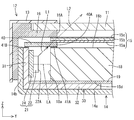
- FIG. 1 is an exploded perspective view showing a schematic configuration of a television receiver according to the present embodiment
- FIG. 2 is an exploded perspective view showing a schematic configuration of a liquid crystal display device
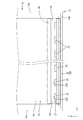
- FIG. 3 is a cross-sectional configuration along the short side direction of the liquid crystal display device.
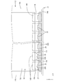
- FIG. 4 is a plan view showing a state in which the backlight device included in the liquid crystal display device is viewed from the front side (light emission side).
- each drawing shows an X-axis, a Y-axis, and a Z-axis, and each axis direction is drawn in a common direction in each drawing.
- the upper side shown in FIG. 3 is the front side (front side, light emission side), and the lower side is the back side (back side, opposite to the light emission side).
- the television receiver TV includes a liquid crystal display device 10 (display device), front and back cabinets Ca and Cb that are accommodated so as to sandwich the liquid crystal display device 10, and a power source P.
- a tuner T and a stand S are provided.
- the liquid crystal display device 10 has a horizontally long rectangular shape (rectangular shape) as a whole and is accommodated in a vertically placed state (a state in which the short side direction is arranged along the vertical direction).
- the liquid crystal display device 10 includes a liquid crystal panel 11 that is a display panel and a backlight device 12 (illumination device) that is an external light source, which are integrated by a frame-like bezel 13 or the like. Is supposed to be retained.
- the liquid crystal panel 11 and the backlight device 12 constituting the liquid crystal display device 10 will be described.
- the liquid crystal panel 11 has a rectangular shape in plan view, and a pair of glass substrates are bonded together with a predetermined gap therebetween, and liquid crystal is sealed between the glass substrates. It is said.
- One glass substrate is provided with a switching element (for example, TFT) connected to a source wiring and a gate wiring orthogonal to each other, a pixel electrode connected to the switching element, an alignment film, and the like.
- the substrate is provided with a color filter and counter electrodes in which colored portions such as R (red), G (green), and B (blue) are arranged in a predetermined arrangement, and an alignment film.
- a polarizing plate (not shown) is disposed outside both substrates.
- the driving of the liquid crystal panel 11 is controlled by a liquid crystal panel control unit (not shown).
- the liquid crystal panel control unit can output a control signal toward the liquid crystal panel 11 and control driving of the liquid crystal panel 11 based on an output signal output from an image signal processing unit (not shown).
- an image signal such as a television broadcast signal input to the tuner T via the antenna is input to the image signal processing unit.
- the input signal is subjected to image processing and the processed signal is processed. Output to a liquid crystal panel control unit or the like is possible.
- the backlight device 12 is disposed so as to cover a substantially box-shaped chassis 14 having an opening on the light emitting surface side (the liquid crystal panel 11 side), and the opening of the chassis 14.
- Optical member 15 group (diffusion sheet 15 a, lens sheet 15 b, reflective polarizing sheet 15 c), a frame disposed along the outer edge portion of the chassis 14 and holding the outer edge portion of the optical member 15 group sandwiched between the chassis 14 16.
- an LED unit 21 in which a plurality of LEDs 22 (Light Emitting Diodes: light sources) are mounted on an LED substrate 24, and a light source mounting member 30 that fixes the LED unit 21 to the chassis 14.
- the light guide plate 18 that guides the light from the LED 22 and guides it to the optical member 15 group side (and thus the liquid crystal panel 11 side), and the light emitted from the LED 22 is not incident on the light guide plate 18 and is not incident on the optical member.
- a light blocking member 40 capable of blocking light (illustrated by an arrow L1 in FIG. 3) toward the 15th group side and a light reflecting sheet 19 disposed on the back side of the light guide plate 18 are provided.
- the backlight device 12 employs a so-called edge light system (side light system) in which the light guide plate 18 is disposed directly below the liquid crystal panel 11 and the LEDs 22 are disposed on the side end portions of the light guide plate 18. Yes.
- the chassis 14 is made of a metal such as an aluminum material, for example. 2 and 3, the chassis 14 has a rectangular bottom plate 14a similar to the liquid crystal panel 11, a pair of long side plates 14b rising from the outer ends of the long sides of the bottom plate 14a, and the bottom plate 14a. And a pair of short side plates 14c rising from the outer end of the short side, and as a whole, has a shallow substantially box shape opening toward the front side.
- the chassis 14 is arranged such that its long side direction coincides with the X-axis direction (horizontal direction) and its short side direction coincides with the Y-axis direction (vertical direction).
- Various substrates (not shown) are attached to the back side of the bottom plate 14 a of the chassis 14, that is, the back side of the backlight device 12.
- Examples of such various boards include a power supply circuit board that supplies power to the liquid crystal panel 11 and the LED 22, an LED control circuit board that controls driving of the LED 22, and a liquid crystal control circuit board that has the liquid crystal panel control unit described above. It can be illustrated.
- the optical member 15 has a rectangular shape in plan view, like the liquid crystal panel 11 and the chassis 14.
- the optical member 15 is configured by laminating a diffusion sheet 15 a, a lens sheet 15 b, and a reflective polarizing sheet 15 c in order from the light guide plate 18 side, and is interposed between the liquid crystal panel 11 and the light guide plate 18.
- Such an optical member 15 has a function of converting light emitted from the light guide plate 18 into planar light.
- the frame 16 has a frame shape similar to the bezel 13 and is fixed to the chassis 14. Further, the inner peripheral end portion of the frame 16 has a step shape, and is configured to receive the outer peripheral edge portion of the liquid crystal panel 11 from the back side.
- the LED unit 21 is attached to one inner surface side of the long side plate 14b of the chassis 14 by, for example, screwing. As shown in FIGS. 2 and 4, the LED unit 21 is configured by linearly arranging a plurality of LEDs 22 on a rectangular LED substrate 24 extending along the X-axis direction.
- the LED 22 has an optical axis LA arranged along a direction (Y-axis direction) parallel to the display surface of the liquid crystal panel 11 or the light emitting surface 18 b of the light guide plate 18.
- the surface 22A is arranged so as to face the side surface (light incident surface 18a) of the light guide plate 18.
- the light emitted from the LED 22 spreads radially to some extent within a predetermined angle range around the optical axis LA, but its directivity is higher than that of, for example, a cold cathode tube. Yes. That is, the light emission intensity of the LED 22 shows an angular distribution in which the direction along the optical axis LA is conspicuously high, and decreases rapidly as the tilt angle with respect to the optical axis LA increases.
- the LED 22 has, for example, a configuration in which a plurality of LED chips that are light emitting elements are sealed in a housing with a resin material or the like.
- the LED 22 includes, for example, three types of LED chips having different main emission wavelengths. Specifically, each LED chip emits R (red), G (green), and B (blue) in a single color. It has become. Thereby, the LED 22 can emit white light.
- the LED 22 is a so-called top type in which the surface opposite to the mounting surface with respect to the light source mounting member 30 is the light emitting surface 22A.
- the configuration of the LED 22 is not limited to this configuration, and may be another configuration.
- the LED 22 incorporates an LED chip that emits B (blue) in a single color, and a phosphor having an emission peak in the R (red) region and a phosphor having an emission peak in the G (green) region are mixed.
- the LED chip may be covered with a formed resin (for example, a silicon-based resin).
- the LED 22 has a built-in LED chip that emits B (blue) in a single color, and covers the LED chip with a resin (for example, a silicon-based resin) mixed with a yellow-emitting phosphor such as a YAG phosphor. It may be.
- the LED substrate 24 is made of, for example, a synthetic resin whose surface (a surface facing the light guide plate 18) has a white color with excellent light reflectivity. As shown in FIG. 2, the LED substrate 24 has a rectangular plate shape extending in the X-axis direction, and its long side dimension is set to a slightly smaller value (or substantially the same value) than the long side dimension of the bottom plate 14a. ing.
- a wiring pattern (not shown) made of a metal film is formed on the LED substrate 24, and each LED 22 is mounted at a predetermined position so as to be electrically connected to the wiring pattern.
- a power supply circuit board and an LED control circuit board are connected to the LED board 24, and power necessary for lighting the LED 22 is supplied from the LED circuit board 24, and drive control of the LED 22 is possible.
- the light source attachment member 30 is for attaching the LED unit 21 (and thus a plurality of LEDs 22) to the chassis 14, and is made of a metal such as the same aluminum material as the chassis 14, for example. As shown in FIG. 2, the light source mounting member 30 has a plate shape extending in the long side direction (X-axis direction) of the chassis 14 and the light guide plate 18.
- the light source mounting member 30 has a bent shape that is L-shaped in cross section. Specifically, the light source mounting member 30 includes one end portion 31 extending in parallel with the light incident surface 18 a of the light guide plate 18 and the other end portion 32 extending in parallel with the bottom plate 14 a of the chassis 14.
- the LED substrate 24 is attached to the one end 31 by, for example, screws.
- the one end portion 31 of the light source mounting member 30 is disposed so as to sandwich the LED 22 with the light incident surface 18a.
- the material and shape of the light source mounting member 30 can be changed as appropriate.
- the other end 32 is fixed to the bottom plate 14a of the chassis 14 with, for example, screws.
- the other end portion 32 is arranged so that the entire surface thereof is in close contact with the bottom plate 14a, and heat generated from the LED 22 is conducted to the other end portion 32 via the LED substrate 24 and the one end portion 31, and the other end portion is provided.
- the heat is transmitted from the portion 32 to the bottom plate 14a of the chassis 14, and is radiated from the bottom plate 14a to the external space. That is, the light source mounting member 30 functions as a heat radiating member capable of effectively radiating the heat of the LED 22 while fixing the LED unit 21 to the chassis 14.
- the light guide plate 18 is made of a synthetic resin material (for example, acrylic) having a refractive index sufficiently higher than air and substantially transparent (exceeding translucency), has a rectangular shape in plan view, and has a predetermined thickness. It is formed in a plate shape. As shown in FIG. 2, the light guide plate 18 is disposed in the chassis 14 immediately below the liquid crystal panel 11 and the optical member 15. Specifically, the main plate surface (light emitting surface 18 b) of the light guide plate 18 is directed to the front side (optical member 15 side) and is arranged in parallel along the display surface of the liquid crystal panel 11.
- a synthetic resin material for example, acrylic
- the main plate surface (light emitting surface 18 b) of the light guide plate 18 is directed to the front side (optical member 15 side) and is arranged in parallel along the display surface of the liquid crystal panel 11.
- the side surface on the long side arranged to face the light emitting surface 22 ⁇ / b> A of the LED 22 is a light incident surface 18 a on which light from the LED 22 is incident.
- the main plate surface arranged on the front side (optical member 15 side) of the light guide plate 18 is a light emitting surface 18b for emitting light from the LED 22 incident from the light incident surface 18a (see FIGS. 2 and 3). .
- the light guide plate 18 introduces the light emitted from the LED 22 in the Y-axis direction from the light incident surface 18a and directs the light toward the optical member 15 side (Z-axis direction) while propagating the light inside. And has a function of emitting from the light exit surface 18b.
- a plurality of light reflecting portions are formed on a surface 18d (surface on the back side) opposite to the light emitting surface 18b.
- the light reflecting section is configured by a white dot pattern and has a function of scattering and reflecting light. Accordingly, light that is scattered and reflected by the light reflecting portion and travels toward the light exit surface 18b is light whose incident angle with respect to the light exit surface 18b does not exceed the critical angle (light that is not totally reflected), and thus the light is emitted from the light exit surface.
- the light can be emitted from the liquid crystal panel 11 side from 18b.
- Such a light reflecting portion is configured by arranging, for example, a plurality of dots having a round shape in plan view in a zigzag shape (staggered shape, staggered shape). Each dot is formed, for example, by printing a paste containing a metal oxide on the back surface 18 d of the light guide plate 18.
- the printing means screen printing, ink jet printing and the like are suitable.
- a light reflection sheet 19 is laid on the bottom plate 14 a of the chassis 14.
- the light reflecting sheet 19 has a rectangular shape in plan view, and is disposed so as to cover the entire area of the back surface 18d of the light guide plate 18 and the LED unit 21 from the back side.
- the light reflecting sheet 19 is made of, for example, a synthetic resin, and the surface thereof is white with excellent light reflectivity.
- the light reflecting sheet 19 has a function of causing the light emitted from the LED 22 to the light reflecting sheet 19 side to be incident on the light incident surface 18 a of the light guide plate 18.
- the material, color, etc. of the light reflection sheet 19 are not limited to those of the present embodiment, and any material having a function of reflecting light may be used.
- the light shielding member 40 is made of, for example, a synthetic resin having a melting point of 100 ° C. or higher, and extends in the longitudinal direction (X-axis direction) of the light guide plate 18 and the LED substrate 24 as shown in FIGS. I am doing.
- the material of the light shielding member 40 can be appropriately changed, and the melting point is not limited to 100 ° C. or higher.
- the light shielding member 40 has one end in the short side direction fixed to the light guide plate 18 and the other end in the short side direction fixed to the light source mounting member 30. . More specifically, one end portion of the light shielding member 40 in the short side direction (left and right direction in FIG. 3) is an end portion on the LED 22 side on the light emitting surface side of the light guide plate 18 through an adhesive layer 41A made of an adhesive or the like. It is fixed to. Further, the other end portion in the short side direction of the light shielding member 40 is fixed to the light emitting surface side of the light source mounting member 30 via the adhesive layer 41B.
- the light shielding member 40 is disposed so as to straddle both the light guide plate 18 and the light source mounting member 30, and is interposed between the optical member 15 group and the light guide plate 18, and the LED 22 is arranged on the light emitting surface 18b side. It is the structure which covers from (upper side of FIG. 3).
- the length of the light shielding member 40 in the longitudinal direction is set to be substantially the same as the entire length of the LED substrate 24, and the light shielding member 40 includes a plurality of LEDs 22 on the light emitting surface 18 b of the light guide plate 18. It is arranged in a form that covers it from the side.
- the light shielding member 40 is illustrated by a two-dot chain line.
- the light L1 (refer to FIG. 3) that is not incident on the light guide plate 18 and is directed to the optical member 15 side out of the light from the light emitting surface 22A of the LED 22 can be shielded by the light shielding member 40.
- the end face 40A on the inner side of the chassis 14 in the light shielding member 40 is arranged on the outer side (left side in FIG. 3) of the chassis 14 with respect to the inner peripheral end face 16A in the frame 16.
- This embodiment is configured as described above, and its operation will be described next.
- the drive of the liquid crystal panel 11 is controlled by a liquid crystal panel control unit (not shown), and the drive of each LED 22 in the backlight device 12 is controlled by the LED control circuit board.
- the illumination light is irradiated to the liquid crystal panel 11, and a predetermined image is displayed on the liquid crystal panel 11.
- each LED 22 when each LED 22 is lit by being driven, the light emitted from the light emitting surface 22A of each LED 22 enters the light guide plate 18 from the light incident surface 18a of the light guide plate 18. After that, the light incident on the light guide plate 18 is guided in the light guide plate 18 by total reflection, and is scattered and reflected by the light reflecting portion, and is emitted from the light exit surface 18b. Then, the outgoing light from the light outgoing surface 18 b passes through the optical member 15 and is then irradiated on the back side of the liquid crystal panel 11.
- the light emitted from the light emitting surface 22A of the LED 22 spreads radially around the optical axis LA. For this reason, a part of the light emitted from the light emitting surface 22A (such light is indicated by an arrow L1 in FIG. 3) is not incident on the light incident surface 18a of the light guide plate 18 and is directly optical. There is concern about the situation of being emitted toward the member 15 side.
- Such light that is not incident on the light incident surface 18a but is directly emitted to the optical member 15 side is disposed by bringing the light emitting surface 22A of the LED 22 and the light incident surface 18a of the light guide plate 18 close to each other. Can be reduced to some extent. However, in consideration of assembly errors and thermal expansion of each member, it is difficult to bring the light emitting surface 22A of the LED 22 into contact with the light incident surface 18a of the light guide plate 18, and a certain gap is generated between both surfaces. It will be. For this reason, it is difficult to completely suppress the light that is not incident on the light incident surface 18a and is directly emitted to the optical member 15 side.
- the light shielding member 40 is disposed so as to straddle both the light guide plate 18 and the light source mounting member 30, and covers the LED 22 from the light emitting surface 18b side (upper side in FIG. 3). It has become.
- region between the light-guide plate 18 and the light source attachment member 30 among the light from 22 A of light emission surfaces, and can go to the light-projection surface side can be light-shielded by the light shielding member 40, and a brightness nonuniformity is produced. The situation that occurs can be suppressed.
- the backlight device 12 includes the LED 22 having the light emitting surface 22A, the light incident surface 18a that is arranged to face the light emitting surface 22A and receives light from the light emitting surface 22A.
- the light source plate 18 having the light emitting surface 18b for emitting the light incident from the light incident surface 18a and the light incident surface 18a are arranged so as to sandwich the LED 22 and the light source mounting member to which the LED 22 is attached 30 and a light shielding member 40 which is fixed to both the light emitting surface 18b end of the light guide plate 18 on the LED 22 side and the light source mounting member 30 and can shield light from the light emitting surface 22A.
- a light shielding member 40 capable of shielding light from the LED 22 is provided.
- region between the light-guide plate 18 and the light source attachment member 30 among light from 22 A of light emission surfaces, and goes to the light-projection surface 18b side can be light-shielded by the light shielding member 40.
- the light that is not incident on the light guide plate 18 and travels toward the light exit surface 18b can be shielded, and uneven brightness can be suppressed.
- the light shielding member 40 is fixed to both the end portion of the light guide plate 18 on the LED 22 side and the light source mounting member 30. For this reason, the situation which a clearance gap produces between the light shielding member 40 and the light-guide plate 18, or the light shielding member 40 and the light source attachment member 30 can be suppressed, and the situation where light leaks can be suppressed.
- the present embodiment it is possible to reduce the situation where light that is not incident on the light guide plate 18 and is directed to the light exit surface side is emitted from the backlight device 12, and it is possible to suppress the occurrence of uneven brightness. Further, according to the configuration of the present embodiment, since the light shielding member 40 is fixed to both the light guide plate 18 and the light source attachment member 30, the light guide plate 18 is attached to the light source attachment member 30 via the light shielding member 40. It can be fixed more reliably. For this reason, for example, the situation where the light guide plate 18 vibrates due to the vibration when the backlight device 12 is driven can be suppressed, and the situation where the light guide plate 18 is damaged can be more reliably suppressed.
- a plurality of LEDs 22 are attached to the light source attachment member 30, and the light shielding member 40 is arranged so as to collectively cover the plurality of LEDs 22 from the light emitting surface 18b side.
- the light emitted from each LED 22 can be blocked by the light blocking member 40.
- the plurality of LEDs 22 are collectively covered by the light shielding member 40. For this reason, the workability
- the melting point of the light shielding member 40 is set at 100 ° C. or higher.
- the light shielding member 40 is melted and deformed by the heat generated from the LED 22, and the quality (the light shielding performance and the function of fixing the light guide plate 18 to the light source mounting member 30) is deteriorated. Can be suppressed.
- the light source is an LED as in the present embodiment
- the melting point of the light shielding member 40 may be 85 ° C. or higher under the usage environment (85 ° C. or lower) of the backlight device 12 described above. The quality of the member 40 can be maintained.
- LED22 is used as a light source. Power consumption can be suppressed by using LEDs.
- the light shielding member 140 of the present embodiment is formed by laminating a light reflecting layer 140A and a heat conduction layer 140B (heat conduction portion).
- the light reflecting layer 140A is disposed on the LED 22 side of the light shielding member 140, and has, for example, the same configuration as the light reflecting sheet 19, that is, made of a synthetic resin, and has a white surface with excellent light reflectivity. It is said.
- the LED 22 side surface of the light shielding member 140 (light reflection layer 140A) is a light reflection surface 140A1.
- the light reflecting surface 140A1 is arranged in such a manner that the light from the LED 22 is reflected toward the light incident surface 18a of the light guide plate 18.
- light from the LED 22 can be reflected to the light guide plate 18 side by the light reflecting surface 140A1 of the light shielding member 140 (such light is indicated by an arrow L3 in FIG. 5).
- the light from LED22 can be more reliably entered in the light guide plate 18, and the brightness
- the heat conductive layer 140B is made of a material having a high thermal conductivity (thermal conductivity) such as a metal, and is preferably made of a material having a higher thermal conductivity than the light reflecting layer 140A.
- the light shielding member 140 is fixed to both the light source mounting member 30 and the light guide plate 18. Therefore, if the light shielding member 140 includes the heat conductive layer 140B, the heat generated when the LED 22 emits light is thermally conducted in the order of the light source mounting member 30, the light shielding member 140 (particularly the heat conductive layer 140B), and the light guide plate 18. It is possible to dissipate heat more effectively. Thereby, the temperature rise of LED22 can be suppressed and the fall of luminous efficiency, thermal degradation, etc. can be suppressed.
- the thickness of the heat conductive layer 140B is set to be greater than the thickness of the light reflecting layer 140A. It is preferable to set a large value.
- the material of the heat conductive layer 140B is not limited to a metal, for example, a silicone rubber sheet may be used.
- the light reflecting layer 140A is configured to cover almost the entire surface of the heat conductive layer 140B from the LED 22 side, but is not limited thereto.
- the light reflecting layer 140A is fixed to each of the light source mounting member 30 and the light guide plate 18 via the adhesive layers 41A and 41B, but is not limited thereto.
- the heat conductive layer 140B may be configured to be fixed to each of the light source mounting member 30 and the light guide plate 18 via the adhesive layers 41A and 41B.
- the plurality of LEDs 22 are collectively covered by the light shielding member 40.
- a plurality of light shielding members 140 according to the present embodiment are arranged corresponding to the plurality of LEDs 22.
- each light shielding member 140 covers each LED 22 from the light emitting surface 18b side (the upper side in FIG. 5).
- each LED 22 can be blocked (and thus reflected) by each light blocking member 140. Further, according to the present embodiment, each of the plurality of LEDs 22 is covered with each light shielding member 140. For this reason, compared with the structure which covers several LED22 collectively with one sheet of light shielding member, the total area of a light shielding member can be decreased and the cost concerning a light shielding member can be reduced.
- each light shielding member 140 is set in the X-axis direction of the emission range of light emitted from the LED 22 (indicated by a one-dot chain line L4 in FIG. 6). It is preferable to set a value larger than the length. Thereby, the situation where light leaks from the gaps between the respective light shielding members 140 can be suppressed, and the light emitted from the LEDs 22 can be more reliably shielded.
- variety of each light shielding member 140 can be changed suitably.
- Embodiment 3 of the present invention will be described with reference to FIG.
- the same parts as those in the above embodiment are denoted by the same reference numerals, and redundant description is omitted.
- the LED unit 21 is attached to the inner surface of the long side plate 14 b of the chassis 14. That is, in this embodiment, the long side plate 14b of the chassis 14 corresponds to the light source mounting member.
- the light shielding member 240 is fixed to both the light guide plate 18 and the long side plate 14b.
- the configuration of the light shielding member 240 is different from the above embodiment.
- the light shielding member 240 of the present embodiment is made of a material having light reflectivity (for example, white beads or powdered aluminum) on an adhesive material (for example, a synthetic rubber-based resin material or an acrylic-based synthetic resin material). Etc.) is dispersed and blended and formed into a plate shape.
- the light shielding member 240 has a light reflective surface on the LED 22 side, and does not include the adhesive layer 41 as in the above embodiments, and the long side plate 14b (light source mounting member) and the light guide of the chassis 14.
- the optical plate 18 can be fixed (adhered) to the optical plate 18.
- the light-shielding member 240 can be made to have higher thermal conductivity by including a material having excellent thermal conductivity such as powdered aluminum.
- the light shielding member 240 is composed of each layer (light reflecting layer 140A, heat conductive layer 140B, adhesive layers 41A, 41B) as in the above embodiments. In comparison, workability related to assembly can be improved.
- the configuration in which the light shielding members 40 and 140 are fixed to the light source mounting member 30 and the light guide plate 18 by the adhesive layer 41 such as an adhesive is exemplified, but the present invention is not limited thereto.
- the light shielding members 40 and 140 may be fixed to the light source mounting member 30 and the light guide plate 18 by heat welding or the like.
- the shape and material of the light shielding members 40, 140, and 240 are not limited to those exemplified in the above embodiment, and can be changed as appropriate.
- the configuration of the optical member 15 group is not limited to that exemplified in the above embodiment.
- the presence / absence of each sheet constituting the optical member 15 and the number of sheets used can be changed as appropriate.
- an LED light emitting diode
- the present invention is not limited to this.
- a light source other than an LED such as a cold cathode tube, can be applied.
- the TFT is used as the switching element of the liquid crystal display device.
- the present invention can also be applied to a liquid crystal display device using a switching element other than TFT (for example, a thin film diode (TFD)), and color display.
- a switching element other than TFT for example, a thin film diode (TFD)
- color display for example, a liquid crystal display device.
- the present invention can be applied to a liquid crystal display device that displays black and white.
- the liquid crystal display device using the liquid crystal panel as the display panel has been exemplified, but the present invention can also be applied to a display device using another type of display panel.
- the television receiver provided with the tuner is exemplified, but the present invention can also be applied to a display device not provided with the tuner.
- SYMBOLS 10 Liquid crystal display device (display device), 11 ... Liquid crystal panel (display panel), 12, 112, 212 ... Backlight device (illumination device), 14b ... Long side plate (light source attachment member) of chassis, 18 ... Lead Light plate, 18a ... light incident surface, 18b ... light emitting surface, 22 ... LED (light source, light emitting diode), 22A ... light emitting surface, 30 ... light source mounting member, 40, 140, 240 ... light shielding member, 140A1 ... light reflecting surface, 140B ... heat conduction layer (heat conduction part), TV ... TV receiver
Landscapes
- Physics & Mathematics (AREA)
- General Physics & Mathematics (AREA)
- Optics & Photonics (AREA)
- Nonlinear Science (AREA)
- Mathematical Physics (AREA)
- Chemical & Material Sciences (AREA)
- Crystallography & Structural Chemistry (AREA)
- Planar Illumination Modules (AREA)
Abstract
本発明に係る照明装置は、発光面22Aを有するLED22と、発光面22Aと対向状に配されるとともに発光面22Aからの光が入射される光入射面18a及び、光入射面18aから入射された光を出射させる光出射面18bを有する導光板18と、光入射面18aとの間でLED22を挟む形で配されるとともに、LED22が取り付けられる光源取付部材30と、導光板18の光出射面18b側におけるLED22側の端部及び光源取付部材30の双方に対してそれぞれ固着され、発光面22Aからの光を遮光可能な遮光部材40と、を備えている。
Description
本発明は、照明装置、表示装置、及びテレビ受信装置に関する。
近年、画像表示装置の表示素子としては、液晶パネルやプラズマディスプレイパネルなどの薄型表示素子が用いられ、画像表示装置の薄型化を可能としている。表示素子として液晶パネルを用いた場合、液晶パネルは自発光しないため、別途に照明装置(バックライト装置)を必要としている。
このような照明装置の一例として下記特許文献1に記載されたものが知られている。この照明装置は、光源(例えば、LEDなどの発光体)と、光源からの光を液晶パネルの表示面に向けて出射させる導光板とを備える。より具体的に説明すると、光源は、その出射光が導光板の光入射面に向かう形で配されており、光入射面から入射した光は、導光板内で全反射を繰り返すことで導光され、光出射面から出射される。
(発明が解決しようとする課題)
上記特許文献のように、光源と導光板を備えた構成の場合、光源からの光を導光板に漏れなく入射させることが好ましい。なぜなら、光源からの光が導光板に入射されず直接的に液晶パネルの表示面に向かうと、光源側の端部において輝度が高くなってしまい輝度ムラの原因となるためである。光源からの光を導光板に漏れなく入射させるためには、光源の発光面と導光板の光入射面とをできるだけ接近させて配することが好ましい。しかしながら、導光板の熱による膨張や各部品の組み付け誤差などを考慮すると、光源の発光面と導光板の光入射面とはわずかに隙間を空けて配することが好ましい。このため、光が光源と導光板との隙間を通過し、導光板に入射されず液晶パネルに向かう事態が懸念される。
上記特許文献のように、光源と導光板を備えた構成の場合、光源からの光を導光板に漏れなく入射させることが好ましい。なぜなら、光源からの光が導光板に入射されず直接的に液晶パネルの表示面に向かうと、光源側の端部において輝度が高くなってしまい輝度ムラの原因となるためである。光源からの光を導光板に漏れなく入射させるためには、光源の発光面と導光板の光入射面とをできるだけ接近させて配することが好ましい。しかしながら、導光板の熱による膨張や各部品の組み付け誤差などを考慮すると、光源の発光面と導光板の光入射面とはわずかに隙間を空けて配することが好ましい。このため、光が光源と導光板との隙間を通過し、導光板に入射されず液晶パネルに向かう事態が懸念される。
本発明は上記のような事情に基づいて完成されたものであって、輝度ムラを低減可能な照明装置を提供することを目的とする。また、このような照明装置を備えた表示装置、及びテレビ受信装置を提供することを目的とする。
(課題を解決するための手段)
上記課題を解決するために、本発明の照明装置は、発光面を有する光源と、前記発光面と対向状に配されるとともに前記発光面からの光が入射される光入射面及び、前記光入射面から入射された光を出射させる光出射面を有する導光板と、前記光入射面との間で前記光源を挟む形で配されるとともに、前記光源が取り付けられる光源取付部材と、前記導光板の前記光出射面側における前記光源側の端部及び前記光源取付部材の双方に対してそれぞれ固着され、前記発光面からの光を遮光可能な遮光部材と、を備えていることに特徴を有する。
上記課題を解決するために、本発明の照明装置は、発光面を有する光源と、前記発光面と対向状に配されるとともに前記発光面からの光が入射される光入射面及び、前記光入射面から入射された光を出射させる光出射面を有する導光板と、前記光入射面との間で前記光源を挟む形で配されるとともに、前記光源が取り付けられる光源取付部材と、前記導光板の前記光出射面側における前記光源側の端部及び前記光源取付部材の双方に対してそれぞれ固着され、前記発光面からの光を遮光可能な遮光部材と、を備えていることに特徴を有する。
本発明においては、導光板の光出射面側における光源側の端部及び光源取付部材の双方に対してそれぞれ固着され、光源からの光を遮光可能な遮光部材を備えている。これにより、発光面からの光のうち、導光板と光源取付部材の間の領域を通過して、光出射面側に向かう光を遮光部材によって遮光することができる。言い換えると、導光板に入射されず光出射面側に向かう光を遮光でき、輝度ムラが発生する事態を抑制できる。さらに、本発明においては、遮光部材は、導光板における光源側の端部及び光源取付部材の双方に対して、それぞれ固着されている。このため、遮光部材と導光板、又は遮光部材と光源取付部材との間に隙間が生じる事態を抑制でき、光が漏れる事態を抑制できる。以上のことから、本発明によれば、導光板に入射されず光出射面側に向かう光を低減でき、輝度ムラが生じる事態を抑制できる。また、本発明の構成によれば、遮光部材が導光板及び光源取付部材の双方に固着されているから、遮光部材を介して、光源取付部材に対して導光板をより確実に固定することができる。このため、例えば、照明装置駆動時の振動などによって導光板が振動する事態を抑制でき、導光板が損傷する事態をより確実に抑制できる。
上記構成において、前記遮光部材における前記光源側の面のうち、少なくとも一部は、光反射面とされ、前記光反射面は、前記光源からの光を前記導光板の前記光入射面に向けて反射させる形で配されているものとすることができる。
このような構成とすれば、遮光部材の光反射面によって、光源からの光を導光板側へ反射させることができる。これにより、光源からの光をより確実に導光板に入射させることができ、導光板の光出射面から出射される光の輝度をより高くすることができる。
また、前記遮光部材は、前記光源から発生する熱を前記導光板に熱伝導可能な熱伝導部を有するものとすることができる。
本発明において、遮光部材は光源取付部材及び導光板の双方に固着されている。このため、遮光部材が熱伝導部を有する構成とすれば、発光時に光源から発生する熱は、光源取付部材、遮光部材(熱伝導部)、導光板の順に熱伝導され、より効果的に放熱することができる。これにより、光源の温度上昇を抑制でき、発光効率の低下や熱劣化等を抑制できる。
また、前記光源は、前記光源取付部材に対して複数取り付けられ、前記遮光部材は、複数の前記光源を前記光出射面側から一括して覆う形で配されているものとすることができる。
このような構成とすれば、各光源から出射される光を遮光部材にて遮光することができる。本発明によれば、複数の光源を遮光部材によって一括して覆うようにしている。このため、各光源を複数の遮光部材でそれぞれ覆う構成と比較して、遮光部材を組み付ける際の作業性を向上させることができる。
また、前記光源は、前記光源取付部材に対して複数取り付けられ、前記遮光部材は、複数の前記光源の各々を前記光出射面側からそれぞれ覆う形で複数配されているものとすることができる。
このような構成とすれば、各光源から出射される光を各遮光部材にて遮光することができる。また、本発明によれば、複数の光源の各々を各遮光部材によってそれぞれ覆うようにしている。このため、各光源を一括して遮光部材で覆う構成と比較して、遮光部材の総面積を少なくすることができ、遮光部材に係るコストを低減することができる。
また、前記遮光部材は、その融点が100℃以上で設定されているものとすることができる。
このような構成とすれば、光源から発する熱によって、遮光部材が溶融することで変形し、その品質(遮光性能や光源取付部材に対して導光板を固定する機能)が低下する事態を抑制できる。仮に光源が発光ダイオードの場合、熱による発光効率の低下を防止するためには、例えば、85℃以下の使用環境にて使用することが好ましいとされる。このため、遮光部材の融点を100℃以上とすることで、照明装置の使用環境下において、より確実に遮光部材の品質を保持することができる。
また、前記光源としては、発光ダイオードを例示することができる。発光ダイオードを使用することで消費電力を抑えることができる。
次に、上記課題を解決するために、本発明の表示装置は、上述した照明装置と、前記照明装置からの光を利用して表示を行う表示パネルと、を備えることを特徴とする。
また、前記表示パネルとしては液晶パネルを例示することができる。このような表示装置は液晶表示装置として、種々の用途、例えばテレビやパソコンのデスクトップ画面等に適用でき、特に大型画面用として好適である。
次に、上記課題を解決するために、本発明のテレビ受信装置は、上記表示装置を備えることを特徴とする。
(発明の効果)
本発明によれば、輝度ムラを低減可能な照明装置を提供することができる。また、このような照明装置を備えた表示装置、及びテレビ受信装置を提供することが可能となる。
本発明によれば、輝度ムラを低減可能な照明装置を提供することができる。また、このような照明装置を備えた表示装置、及びテレビ受信装置を提供することが可能となる。
<実施形態1>
本発明の実施形態1を図1ないし図4によって説明する。まず、液晶表示装置10を備えたテレビ受信装置TVの構成について説明する。図1は本実施形態に係るテレビ受信装置の概略構成を示す分解斜視図、図2は液晶表示装置の概略構成を示す分解斜視図、図3は液晶表示装置の短辺方向に沿った断面構成を示す断面図、図4は液晶表示装置が備えるバックライト装置を表側(光出射側)から視た状態を示す平面図である。なお、各図面の一部にはX軸、Y軸及びZ軸を示しており、各軸方向が各図面で共通した方向となるように描かれている。また、図3に示す上側を表側(正面側、光出射側)とし、同下側を裏側(背面側、光出射側とは反対側)とする。
本発明の実施形態1を図1ないし図4によって説明する。まず、液晶表示装置10を備えたテレビ受信装置TVの構成について説明する。図1は本実施形態に係るテレビ受信装置の概略構成を示す分解斜視図、図2は液晶表示装置の概略構成を示す分解斜視図、図3は液晶表示装置の短辺方向に沿った断面構成を示す断面図、図4は液晶表示装置が備えるバックライト装置を表側(光出射側)から視た状態を示す平面図である。なお、各図面の一部にはX軸、Y軸及びZ軸を示しており、各軸方向が各図面で共通した方向となるように描かれている。また、図3に示す上側を表側(正面側、光出射側)とし、同下側を裏側(背面側、光出射側とは反対側)とする。
本実施形態に係るテレビ受信装置TVは、図1に示すように、液晶表示装置10(表示装置)と、当該液晶表示装置10を挟むようにして収容する表裏両キャビネットCa,Cbと、電源Pと、チューナーTと、スタンドSとを備えて構成される。液晶表示装置10は、全体として横長の方形(矩形状)をなし、縦置き状態(短辺方向が鉛直方向に沿って配された状態)で収容されている。この液晶表示装置10は、図2に示すように、表示パネルである液晶パネル11と、外部光源であるバックライト装置12(照明装置)とを備え、これらが枠状のベゼル13などにより一体的に保持されるようになっている。
次に、液晶表示装置10を構成する液晶パネル11及びバックライト装置12について説明する。液晶パネル11は、図2に示すように、平面視矩形状をなしており、一対のガラス基板が所定のギャップを隔てた状態で貼り合わせられるとともに、両ガラス基板間に液晶が封入された構成とされる。一方のガラス基板には、互いに直交するソース配線とゲート配線とに接続されたスイッチング素子(例えばTFT)と、そのスイッチング素子に接続された画素電極、さらには配向膜等が設けられ、他方のガラス基板には、R(赤色),G(緑色),B(青色)等の各着色部が所定配列で配置されたカラーフィルタや対向電極、さらには配向膜等が設けられている。なお、両基板の外側には偏光板(図示せず)が配されている。
この液晶パネル11は、図示しない液晶パネル制御部によってその駆動が制御されるようになっている。この液晶パネル制御部は、図示しない画像信号処理部から出力された出力信号に基づいて、液晶パネル11へ向けて制御信号を出力するとともに液晶パネル11の駆動を制御することができる。この液晶パネル制御部による制御と協働してバックライト装置12から光が供給されることで、液晶パネル11の表示画面に所望の画像を表示することが可能とされる。画像信号処理部には、アンテナを介してチューナーTに入力されたテレビジョン放送信号などの画像信号が入力されるようになっており、その入力された信号を画像処理するとともに、処理した信号を液晶パネル制御部等に出力可能とされる。
バックライト装置12は、図2に示すように、光出射面側(液晶パネル11側)に開口部を有した略箱型をなすシャーシ14と、シャーシ14の開口部を覆うようにして配される光学部材15群(拡散シート15a、レンズシート15b、反射型偏光シート15c)、シャーシ14の外縁部に沿って配され光学部材15群の外縁部をシャーシ14との間で挟んで保持するフレーム16とを備える。
シャーシ14内には、LED基板24上にLED22(Light Emitting Diode:発光ダイオード、光源)が複数個実装されてなるLEDユニット21と、LEDユニット21をシャーシ14に対して固定する光源取付部材30と、LED22からの光を導光して光学部材15群側(ひいては、液晶パネル11側)へと導く導光板18と、LED22から出射される光のうち、導光板18に入射されず、光学部材15群側へ向かう光(図3の矢線L1で図示)を遮光可能な遮光部材40と、導光板18の裏側に配される光反射シート19とが設けられている。このバックライト装置12は、導光板18が液晶パネル11の直下に配されていると共にLED22が導光板18の側端部に配されてなる、いわゆるエッジライト方式(サイドライト方式)を採用している。
次にバックライト装置12の各構成部品について詳しく説明する。シャーシ14は、例えば、アルミ系材料等の金属製とされる。シャーシ14は、図2及び図3に示すように、液晶パネル11と同様に矩形状をなす底板14aと、底板14aのうち長辺の外端から立ち上がる一対の長辺側側板14bと、底板14aのうち短辺の外端から立ち上がる一対の短辺側側板14cとからなり、全体としては表側に向けて開口した浅い略箱型をなしている。
シャーシ14は、その長辺方向がX軸方向(水平方向)と一致し、短辺方向がY軸方向(鉛直方向)と一致する形で配される。なお、シャーシ14の底板14aの裏側、つまりバックライト装置12の背面側には、図示しない各種基板が取り付けられている。このような各種基板としては、例えば、液晶パネル11及びLED22に電力を供給する電源回路基板、LED22の駆動を制御するLED制御回路基板、既述した液晶パネル制御部を有する液晶制御回路基板等を例示することができる。
光学部材15は、図2に示すように、液晶パネル11及びシャーシ14と同様に平面視にて矩形状をなしている。光学部材15は、導光板18側から順に拡散シート15a、レンズシート15b、反射型偏光シート15cが積層されて構成されており、液晶パネル11と導光板18との間に介在されている。このような光学部材15は、導光板18から出射された光を面状の光とする機能などを有している。
フレーム16は、ベゼル13と同様に枠状をなし、シャーシ14に対して固定される。またフレーム16の内周端部は、段差状をなしており、液晶パネル11の外周縁部をその裏側から受ける構成となっている。
LEDユニット21は、シャーシ14の長辺側側板14bのうち、一方における内面側に例えばビス留め等により取り付けられている。LEDユニット21は、図2及び図4に示すように、X軸方向に沿って延びる矩形状をなすLED基板24に、複数のLED22が直線状に配列されることで構成されている。
図3に示すように、LED22は、その光軸LAが、液晶パネル11の表示面又は導光板18の光出射面18bと並行する方向(Y軸方向)に沿って配されており、その発光面22Aが導光板18の側面(光入射面18a)を向く形で配されている。なお、LED22から発せられる光は、光軸LAを中心にして所定の角度範囲内で三次元的にある程度放射状に広がるのであるが、その指向性は、例えば冷陰極管などと比べると高くなっている。つまり、LED22の発光強度は、光軸LAに沿った方向が際立って高く、光軸LAに対する傾き角度が大きくなるに連れて急激に低下するような傾向の角度分布を示す。
LED22は、例えば、発光素子である複数のLEDチップを樹脂材などでハウジング内に封止した構成とされる。このLED22は、例えば、主発光波長の異なる3種類のLEDチップを内蔵しており、具体的には各LEDチップがR(赤色)、G(緑色)、B(青色)を単色発光するようになっている。これにより、LED22は白色発光することが可能となっている。このLED22は、光源取付部材30に対する実装面とは反対側の面が発光面22Aとなる、いわゆるトップ型とされる。
なお、LED22の構成は、この構成に限定されず、他の構成であってもよい。例えば、LED22は、B(青色)を単色発光するLEDチップを内蔵し、R(赤色)の領域に発光ピークを持つ蛍光体及び、G(緑色)の領域に発光ピークを持つ蛍光体とが混入された樹脂(例えばシリコン系樹脂)で、そのLEDチップを覆った構成であってもよい。また、LED22は、B(青色)を単色発光するLEDチップを内蔵し、YAG蛍光体などの黄色を発光する蛍光体が混入された樹脂(例えばシリコン系樹脂)で、そのLEDチップを覆った構成であってもよい。
LED基板24は、例えば、表面(導光板18との対向面)が光の反射性に優れた白色を呈する合成樹脂製とされている。LED基板24は、図2に示すように、X軸方向に延びる矩形板状をなし、その長辺寸法は、底板14aの長辺寸法より、わずかに小さい値(又はほぼ同じ値)で設定されている。
LED基板24には、金属膜からなる配線パターン(不図示)が形成され、各LED22が配線パターンと電気的に接続される形で所定の位置に実装されている。このLED基板24には、図示しない電源回路基板及びLED制御回路基板が接続されており、そこからLED22の点灯に必要な電力が供給されるとともにLED22の駆動制御が可能となっている。
光源取付部材30は、LEDユニット21(ひいては複数のLED22)をシャーシ14に対して取り付けるためのもので、例えば、シャーシ14と同じアルミ系材料等の金属製からなる。光源取付部材30は、図2に示すように、シャーシ14及び導光板18の長辺方向(X軸方向)に延びる板状をなしている。
光源取付部材30は、図3に示すように、断面視L字状をなす形で屈曲した形状をなしている。具体的には、光源取付部材30は、導光板18の光入射面18aと並行する形で延びる一端部31と、シャーシ14の底板14aと並行する形で延びる他端部32とからなる。LED基板24は、一端部31に対して、例えばビスなどによって取り付けられている。言い換えると、光源取付部材30の一端部31は、光入射面18aとの間でLED22を挟む形で配されている。なお、光源取付部材30の材質及び形状は、適宜変更可能である。
また、他端部32は、シャーシ14の底板14aに対して、例えばビスなどによって固定されている。他端部32はその全面が底板14aに密着するように配されており、LED22から発せられた熱は、LED基板24及び一端部31を介して、他端部32に伝導し、当該他端部32からシャーシ14の底板14aに伝導し、その底板14aから外部空間へと放熱される。つまり、光源取付部材30は、LEDユニット21をシャーシ14に対して固定するとともに、LED22の熱を効果的に放熱可能な放熱部材としての機能を担っている。
導光板18は、屈折率が空気よりも十分に高く且つ略透明な(透光性に優れた)合成樹脂材料(例えばアクリル等)からなり、平面視矩形状をなすとともに、所定の厚みを有する板状に形成されている。導光板18は、図2に示すようにシャーシ14内において液晶パネル11及び光学部材15の直下位置に配されている。具体的には、導光板18の主板面(光出射面18b)が表側(光学部材15側)に指向され、液晶パネル11の表示面に沿って並行して配されている。
導光板18のうち、LED22の発光面22Aと対向状に配されている長辺側の側面は、LED22からの光が入射される光入射面18aとされる。導光板18のうち表側(光学部材15側)に配される主板面は、光入射面18aから入射されたLED22からの光を出射させる光出射面18bとされる(図2及び図3参照)。そして、この導光板18は、LED22からY軸方向に向けて発せられた光を光入射面18aから導入するとともに、その光を内部で伝播させつつ光学部材15側(Z軸方向)へ向くように立ち上げて光出射面18bから出射させる機能を有する。
導光板18において、光出射面18bとは反対側の面18d(裏側の面)には、複数の光反射部(図示せず)が形成されている。光反射部は、例えば、白色を呈するドットパターンによって構成され、光を散乱反射させる機能を担っている。従って、光反射部にて散乱反射されて光出射面18bに向かう光には、光出射面18bに対する入射角が臨界角を超えない光(全反射されない光)が生じ、もって光を光出射面18bから、液晶パネル11側へと出射させることが可能とされる。
このような光反射部は、例えば平面視丸形をなす複数のドットをジグザグ状(千鳥状、互い違い状)に配置することで構成されている。各ドットは、例えば金属酸化物が含有されたペーストを導光板18の裏側の面18dに印刷することで形成される。当該印刷手段としては、スクリーン印刷、インクジェット印刷等が好適である。
また、シャーシ14の底板14aには、光反射シート19が敷設されている。光反射シート19は、平面視方形状をなし、導光板18の裏側の面18dのほぼ全域及び、LEDユニット21を裏側から覆う形で配されている。光反射シート19は、例えば、合成樹脂製とされ、表面が光の反射性に優れた白色を呈するものとされる。この光反射シート19によって、導光板18から、光反射シート19側へ出射された光を、再度、光出射面18b側へ反射させることができ、光の利用効率を高くすることができる。また、光反射シート19は、LED22から、光反射シート19側へ出射された光を反射させることで、導光板18の光入射面18aへ入射させる機能を担っている。なお、光反射シート19の材質、色などは、本実施形態のものに限定されるものではなく、光を反射する機能を備えているものであればよい。
遮光部材40は、例えば、融点が100℃以上の合成樹脂製とされ、図2及び図4に示すように、導光板18及びLED基板24の長手方向(X軸方向)に沿って延びる板状をなしている。なお、遮光部材40の材質は適宜変更可能であって、その融点が100℃以上のものに限定されない。
遮光部材40は、図3及び図4に示すように、短辺方向における一端部が導光板18に対して固着され、短辺方向における他端部が光源取付部材30に対して固着されている。より具体的には、遮光部材40の短辺方向(図3の左右方向)における一端部が、接着剤などによる粘着層41Aを介して、導光板18の光出射面側におけるLED22側の端部に固着されている。また、遮光部材40の短辺方向における他端部が、粘着層41Bを介して、光源取付部材30の光出射面側に固着されている。これにより、遮光部材40は、導光板18と光源取付部材30の双方に跨る形で配されるとともに、光学部材15群と導光板18の間に介在されており、LED22を光出射面18b側(図3の上側)から覆う構成となっている。
図4に示すように、遮光部材40の長手方向における長さは、LED基板24の全長とほぼ同じ長さで設定されており、遮光部材40は複数のLED22を導光板18の光出射面18b側から一括して覆う形で配されている。なお、図4においては、遮光部材40を2点鎖線で図示してある。これにより、LED22の発光面22Aからの光のうち、導光板18に入射されず、光学部材15側へ向かう光L1(図3参照)を遮光部材40によって遮光することが可能となっている。なお、遮光部材40の遮光性をより高くするためには、例えば、その表面を光吸収性に優れた黒色などで設定することが好ましい。
また、遮光部材40におけるシャーシ14内側の端面40Aは、フレーム16における内側の周端面16Aよりも、シャーシ14の外側(図3では左側)に配されている。これにより、遮光部材40によって、導光板18の光出射面18bから液晶パネル11に向かって出射される光が遮光される事態を抑制している。
本実施形態は、以上のような構成であって、続いてその作用を説明する。まず、液晶表示装置10の電源をONにすると、図示しない液晶パネル制御部により液晶パネル11の駆動が制御されるとともに、LED制御回路基板によりバックライト装置12における各LED22の駆動が制御されることで液晶パネル11に照明光が照射され、もって液晶パネル11に所定の画像が表示される。
この時、各LED22が駆動することで点灯すると、各LED22の発光面22Aから出射された光は、導光板18の光入射面18aから、導光板18内に入射される。その後、導光板18内に入射した光は、全反射によって導光板18内で導光され、光反射部にて散乱反射されることで、光出射面18bから出射される。そして、光出射面18bからの出射光は、光学部材15を経由した後、液晶パネル11の背面側に照射される。
ここで、LED22の発光面22Aから出射される光は、光軸LAを中心にして放射状に広がる。このため、発光面22Aから出射される光のうち、一部の光(このような光を図3の矢線L1で示す)が導光板18の光入射面18aに入射されず、直接、光学部材15側へ出射される事態が懸念される。
このような、光入射面18aに入射されず、直接的に光学部材15側へ出射される光は、LED22の発光面22Aと導光板18の光入射面18aとを接近させて配することで、ある程度低減することができる。しかしながら、組み付け誤差や、各部材の熱膨張などを考慮すると、LED22の発光面22Aと導光板18の光入射面18aとを当接させることは困難であり、両面の間に、ある程度隙間が生じることとなる。このため、光入射面18aに入射されず、直接光学部材15側へ出射される光を完全に抑制することは困難である。
このような直接的に光学部材15側へ出射される光が、バックライト装置12から出射される(このような光を図3の矢線L2で示す)と、バックライト装置12からの出射光においてLED22に近い側の輝度が相対的に高くなってしまい、輝度ムラの原因となる。この点、本実施形態においては、遮光部材40が、導光板18と光源取付部材30の双方に跨る形で配されており、LED22を光出射面18b側(図3の上側)から覆う構成となっている。これにより、発光面22Aからの光のうち、導光板18と光源取付部材30の間の領域を通過して、光出射面側に向かう光を遮光部材40によって遮光することができ、輝度ムラが発生する事態を抑制できる。
以上、説明したように、本実施形態のバックライト装置12は、発光面22Aを有するLED22と、発光面22Aと対向状に配されるとともに発光面22Aからの光が入射される光入射面18a及び、光入射面18aから入射された光を出射させる光出射面18bを有する導光板18と、光入射面18aとの間でLED22を挟む形で配されるとともに、LED22が取り付けられる光源取付部材30と、導光板18の光出射面18b側におけるLED22側の端部及び光源取付部材30の双方に対してそれぞれ固着され、発光面22Aからの光を遮光可能な遮光部材40と、を備えている。
本実施形態においては、LED22からの光を遮光可能な遮光部材40を備えている。これにより、発光面22Aからの光のうち、導光板18と光源取付部材30の間の領域を通過して、光出射面18b側に向かう光を遮光部材40によって遮光することができる。言い換えると、導光板18に入射されず光出射面18b側に向かう光を遮光でき、輝度ムラを抑制できる。
さらに、本実施形態においては、遮光部材40は、導光板18におけるLED22側の端部及び光源取付部材30の双方に対して、それぞれ固着されている。このため、遮光部材40と導光板18、又は遮光部材40と光源取付部材30との間に隙間が生じる事態を抑制でき、光が漏れる事態を抑制できる。
以上のことから、本実施形態によれば、導光板18に入射されず光出射面側に向かう光が、バックライト装置12から出射される事態を低減でき、輝度ムラが生じる事態を抑制できる。また、本実施形態の構成によれば、遮光部材40が導光板18及び光源取付部材30の双方に固着されているから、遮光部材40を介して、光源取付部材30に対して導光板18をより確実に固定することができる。このため、例えば、バックライト装置12駆動時の振動などによって導光板18が振動する事態を抑制でき、導光板18が損傷する事態をより確実に抑制できる。
上記構成において、LED22は、光源取付部材30に対して複数取り付けられ、遮光部材40は、複数のLED22を光出射面18b側から一括して覆う形で配されている。
このような構成とすれば、各LED22から出射される光を遮光部材40にて遮光することができる。本実施形態によれば、複数のLED22を遮光部材40によって一括して覆うようにしている。このため、各LED22を複数の遮光部材40でそれぞれ覆う構成と比較して、遮光部材40を組み付ける際の作業性を向上させることができる。
また、遮光部材40は、その融点が100℃以上で設定されている。
このような構成とすれば、LED22から発する熱によって、遮光部材40が溶融することで変形し、その品質(遮光性能や光源取付部材30に対して導光板18を固定する機能)が低下する事態を抑制できる。本実施形態のように光源がLEDの場合、熱によるLEDの発光効率の低下を防止するためには、バックライト装置12を例えば、85℃以下の使用環境にて使用することが好ましいとされる。このため、遮光部材40の融点を100℃以上とすることで、バックライト装置12の使用環境下において、より確実に遮光部材40の溶融(又は軟化)による変形などを抑制することができ、その品質を保持することができる。なお、上述したバックライト装置12の使用環境下(85℃以下)であれば、遮光部材40の融点は85℃以上であってもよいが、100℃以上に設定することで、より確実に遮光部材40の品質を保持することができる。
また、光源として、LED22を用いている。LEDを使用することで消費電力を抑えることができる。
<実施形態2>
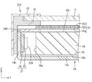
次に、本発明の実施形態2を図5ないし図6によって説明する。上記実施形態と同一部分には、同一符号を付して重複する説明を省略する。本実施形態のバックライト装置112においては、遮光部材140の構成が上記実施形態と相違する。
次に、本発明の実施形態2を図5ないし図6によって説明する。上記実施形態と同一部分には、同一符号を付して重複する説明を省略する。本実施形態のバックライト装置112においては、遮光部材140の構成が上記実施形態と相違する。
本実施形態の遮光部材140は、図5に示すように、光反射層140Aと熱伝導層140B(熱伝導部)とを積層することで形成されている。光反射層140Aは、遮光部材140によるLED22側に配されており、例えば、光反射シート19と同様の構成、すなわち、合成樹脂製とされ、表面が光の反射性に優れた白色を呈するものとされる。これにより、遮光部材140(光反射層140A)におけるLED22側の面は、光反射面140A1とされる。この光反射面140A1は、LED22からの光を導光板18の光入射面18aに向けて反射させる形で配されている。
このような構成とすれば、遮光部材140の光反射面140A1によって、LED22からの光を導光板18側へ反射させることができる(このような光を図5の矢線L3で示す)。これにより、LED22からの光をより確実に導光板18に入射させることができ、導光板18の光出射面18bから出射される光の輝度をより高くすることができる。
一方、熱伝導層140Bは、例えば、金属製などの熱伝導性(熱伝導率)の高い材質とされ、光反射層140Aよりも熱伝導性の高い材質とすることが好ましい。本実施形態において、遮光部材140は光源取付部材30及び導光板18の双方に固着されている。このため、遮光部材140が熱伝導層140Bを有する構成とすれば、LED22発光時に発生する熱は、光源取付部材30、遮光部材140(特に熱伝導層140B)、導光板18の順に熱伝導され、より効果的に放熱することができる。これにより、LED22の温度上昇を抑制でき、発光効率の低下や熱劣化等を抑制できる。
なお、遮光部材140の熱伝導性を高くするためには、熱伝導層140Bの厚さをより大きくすることが好ましく、例えば、熱伝導層140Bの厚さを、光反射層140Aの厚さよりも大きく設定することが好ましい。なお、熱伝導層140Bの材質は、金属に限定されない、例えば、シリコーン系のゴムシートなどを用いてもよい。
なお、本実施形態において、光反射層140Aは、熱伝導層140Bのほぼ全面をLED22側から覆う構成としたが、これに限定されない。また、本実施形態においては、光反射層140Aが粘着層41A,41Bを介して、光源取付部材30及び導光板18の各々と固着されているが、これに限定されない。例えば、熱伝導層140Bが粘着層41A,41Bを介して、光源取付部材30及び導光板18の各々と固着される構成であってもよい。
また、上記実施形態では、遮光部材40によって、複数のLED22を一括して覆う構成とした。これに対して、本実施形態の遮光部材140は、図6に示すように、複数のLED22に対応して複数配されている。つまり、各遮光部材140によって、各LED22を光出射面18b側(図5の上側)からそれぞれ覆う構成となっている。
本実施形態の構成においては、各LED22から出射される光を各遮光部材140にて遮光(ひいては反射)することができる。また、本実施形態によれば、複数のLED22の各々を各遮光部材140によってそれぞれ覆うようにしている。このため、複数のLED22を一括して一枚の遮光部材で覆う構成と比較して、遮光部材の総面積を少なくすることができ、遮光部材に係るコストを低減することができる。
また、各遮光部材140の幅(X軸方向の長さ)は、図6に示すように、LED22から出射される光の出射範囲(図6にて一点鎖線L4で示す)のX軸方向における長さよりも大きい値で設定することが好ましい。これにより、各遮光部材140の隙間から光が漏れる事態を抑制でき、LED22から出射される光をより確実に遮光することができる。なお、各遮光部材140の幅は、適宜変更可能である。
<実施形態3>
次に、本発明の実施形態3を図7によって説明する。上記実施形態と同一部分には、同一符号を付して重複する説明を省略する。本実施形態のバックライト装置212においては、LEDユニット21がシャーシ14の長辺側側板14bにおける内面に取り付けられている。つまり、本実施形態においてはシャーシ14の長辺側側板14bが光源取付部材に対応している。また、遮光部材240は、導光板18と長辺側側板14bの双方にそれぞれ固着されている。
次に、本発明の実施形態3を図7によって説明する。上記実施形態と同一部分には、同一符号を付して重複する説明を省略する。本実施形態のバックライト装置212においては、LEDユニット21がシャーシ14の長辺側側板14bにおける内面に取り付けられている。つまり、本実施形態においてはシャーシ14の長辺側側板14bが光源取付部材に対応している。また、遮光部材240は、導光板18と長辺側側板14bの双方にそれぞれ固着されている。
また、本実施形態においては、遮光部材240の構成が上記実施形態と相違する。本実施形態の遮光部材240は、粘着性を有する材料(例えば、合成ゴム系の樹脂材料やアクリル系の合成樹脂材料など)に、光反射性を有する材料(例えば、白色ビーズや粉末状のアルミなど)を分散配合させ、これを板状に成形することで構成されている。これにより、遮光部材240は、LED22側の面が光反射性を有するとともに、上記各実施形態のような粘着層41を備えずに、シャーシ14の長辺側側板14b(光源取付部材)及び導光板18に対して固着(粘着)させることができる構成となっている。なお、遮光部材240に粉末状のアルミなどといった熱伝導性に優れる材料を含有させることで、遮光部材240の熱伝導性のより高いものとすることができる。
本実施形態のように遮光部材240を一体部品として形成することで、遮光部材が上記各実施形態のように各層(光反射層140A、熱伝導層140B、粘着層41A、41B)からなる構成と比較して、組み付けに係る作業性を向上させることができる。
<他の実施形態>
本発明は上記記述及び図面によって説明した実施形態に限定されるものではなく、例えば次のような実施形態も本発明の技術的範囲に含まれる。
本発明は上記記述及び図面によって説明した実施形態に限定されるものではなく、例えば次のような実施形態も本発明の技術的範囲に含まれる。
(1)上記実施形態では、遮光部材40,140が光源取付部材30及び導光板18に対して、接着剤などの粘着層41によって固着されている構成を例示したが、これに限定されない。例えば、遮光部材40,140が光源取付部材30及び導光板18に対して、熱溶着などで固着されていてもよい。また、遮光部材40,140,240の形状及び材質については、上記実施形態で例示したものに限定されず適宜変更可能である。
(2)上記実施形態で例示した光源(LED22)の実装数は適宜変更可能である。
(3)光学部材15群の構成は、上記実施形態で例示したものに限定されない。光学部材15を構成する各シートの有無、各シートの使用枚数などは適宜変更可能である。
(4)上記実施形態では、光源としてLED(発光ダイオード)を例示したが、これに限定されない。光源としては、LED以外の光源、例えば、冷陰極管などを適用可能である。
(5)上記した実施形態では、液晶表示装置のスイッチング素子としてTFTを用いたが、TFT以外のスイッチング素子(例えば薄膜ダイオード(TFD))を用いた液晶表示装置にも適用可能であり、カラー表示する液晶表示装置以外にも、白黒表示する液晶表示装置にも適用可能である。
(6)上記した実施形態では、表示パネルとして液晶パネルを用いた液晶表示装置を例示したが、他の種類の表示パネルを用いた表示装置にも本発明は適用可能である。
(7)上記した実施形態では、チューナーを備えたテレビ受信装置を例示したが、チューナーを備えていない表示装置にも本発明は適用可能である。
10…液晶表示装置(表示装置)、11…液晶パネル(表示パネル)、12,112,212…バックライト装置(照明装置)、14b…シャーシの長辺側側板(光源取付部材)、18…導光板、18a…光入射面、18b…光出射面、22…LED(光源、発光ダイオード)、22A…発光面、30…光源取付部材、40,140,240…遮光部材、140A1…光反射面、140B…熱伝導層(熱伝導部)、TV…テレビ受信装置
Claims (10)
- 発光面を有する光源と、
前記発光面と対向状に配されるとともに前記発光面からの光が入射される光入射面及び、前記光入射面から入射された光を出射させる光出射面を有する導光板と、
前記光入射面との間で前記光源を挟む形で配されるとともに、前記光源が取り付けられる光源取付部材と、
前記導光板の前記光出射面側における前記光源側の端部及び前記光源取付部材の双方に対してそれぞれ固着され、前記発光面からの光を遮光可能な遮光部材と、を備えていることを特徴とする照明装置。 - 前記遮光部材における前記光源側の面のうち、少なくとも一部は、光反射面とされ、
前記光反射面は、前記光源からの光を前記導光板の前記光入射面に向けて反射させる形で配されていることを特徴とする請求項1に記載の照明装置。 - 前記遮光部材は、前記光源から発生する熱を前記導光板に熱伝導可能な熱伝導部を有することを特徴とする請求項1又は請求項2に記載の照明装置。
- 前記光源は、前記光源取付部材に対して複数取り付けられ、
前記遮光部材は、複数の前記光源を前記光出射面側から一括して覆う形で配されていることを特徴とする請求項1から請求項3のいずれか1項に記載の照明装置。 - 前記光源は、前記光源取付部材に対して複数取り付けられ、
前記遮光部材は、複数の前記光源の各々を前記光出射面側からそれぞれ覆う形で複数配されていることを特徴とする請求項1から請求項3のいずれか1項に記載の照明装置。 - 前記遮光部材は、その融点が100℃以上で設定されていることを特徴とする請求項1から請求項5のいずれか1項に記載の照明装置。
- 前記光源は、発光ダイオードであることを特徴とする請求項1から請求項6のいずれか1項に記載の照明装置。
- 請求項1から請求項7のいずれか1項に記載の照明装置と、
前記照明装置からの光を利用して表示を行う表示パネルと、を備えることを特徴とする表示装置。 - 前記表示パネルが液晶を用いた液晶パネルであることを特徴とする請求項8に記載の表示装置。
- 請求項8又は請求項9に記載された表示装置を備えることを特徴とするテレビ受信装置。
Applications Claiming Priority (2)
| Application Number | Priority Date | Filing Date | Title |
|---|---|---|---|
| JP2011015568 | 2011-01-27 | ||
| JP2011-015568 | 2011-01-27 |
Publications (1)
| Publication Number | Publication Date |
|---|---|
| WO2012102193A1 true WO2012102193A1 (ja) | 2012-08-02 |
Family
ID=46580762
Family Applications (1)
| Application Number | Title | Priority Date | Filing Date |
|---|---|---|---|
| PCT/JP2012/051172 WO2012102193A1 (ja) | 2011-01-27 | 2012-01-20 | 照明装置、表示装置、及びテレビ受信装置 |
Country Status (1)
| Country | Link |
|---|---|
| WO (1) | WO2012102193A1 (ja) |
Cited By (6)
| Publication number | Priority date | Publication date | Assignee | Title |
|---|---|---|---|---|
| CN104061488A (zh) * | 2013-03-18 | 2014-09-24 | 群创光电股份有限公司 | 背光模块及显示装置 |
| CN104501046A (zh) * | 2014-12-24 | 2015-04-08 | 深圳市华星光电技术有限公司 | 窄边框背光模组、移动终端 |
| WO2015186842A1 (ja) * | 2014-06-06 | 2015-12-10 | 恵和株式会社 | エッジライト型バックライトユニット及び反射テープ部材 |
| JPWO2015040699A1 (ja) * | 2013-09-18 | 2017-03-02 | Nltテクノロジー株式会社 | 面状光源装置及び液晶表示装置 |
| WO2017067254A1 (zh) * | 2015-10-21 | 2017-04-27 | 京东方科技集团股份有限公司 | 背光模组及其组装方法和显示装置 |
| EP3690524A4 (en) * | 2017-09-26 | 2020-10-28 | Panasonic Intellectual Property Management Co., Ltd. | IMAGE DISPLAY DEVICE |
Citations (2)
| Publication number | Priority date | Publication date | Assignee | Title |
|---|---|---|---|---|
| JP2005078917A (ja) * | 2003-08-29 | 2005-03-24 | Kawaguchiko Seimitsu Co Ltd | バックライト装置 |
| JP2006064733A (ja) * | 2004-08-24 | 2006-03-09 | Kyocera Corp | 液晶表示装置 |
-
2012
- 2012-01-20 WO PCT/JP2012/051172 patent/WO2012102193A1/ja active Application Filing
Patent Citations (2)
| Publication number | Priority date | Publication date | Assignee | Title |
|---|---|---|---|---|
| JP2005078917A (ja) * | 2003-08-29 | 2005-03-24 | Kawaguchiko Seimitsu Co Ltd | バックライト装置 |
| JP2006064733A (ja) * | 2004-08-24 | 2006-03-09 | Kyocera Corp | 液晶表示装置 |
Cited By (9)
| Publication number | Priority date | Publication date | Assignee | Title |
|---|---|---|---|---|
| CN104061488A (zh) * | 2013-03-18 | 2014-09-24 | 群创光电股份有限公司 | 背光模块及显示装置 |
| JPWO2015040699A1 (ja) * | 2013-09-18 | 2017-03-02 | Nltテクノロジー株式会社 | 面状光源装置及び液晶表示装置 |
| US10495810B2 (en) | 2013-09-18 | 2019-12-03 | Tianma Microelectronics Co., Ltd. | Planar light source device and liquid crystal display apparatus |
| WO2015186842A1 (ja) * | 2014-06-06 | 2015-12-10 | 恵和株式会社 | エッジライト型バックライトユニット及び反射テープ部材 |
| JP2016012562A (ja) * | 2014-06-06 | 2016-01-21 | 恵和株式会社 | エッジライト型バックライトユニット及び反射テープ部材 |
| CN104501046A (zh) * | 2014-12-24 | 2015-04-08 | 深圳市华星光电技术有限公司 | 窄边框背光模组、移动终端 |
| WO2017067254A1 (zh) * | 2015-10-21 | 2017-04-27 | 京东方科技集团股份有限公司 | 背光模组及其组装方法和显示装置 |
| EP3690524A4 (en) * | 2017-09-26 | 2020-10-28 | Panasonic Intellectual Property Management Co., Ltd. | IMAGE DISPLAY DEVICE |
| US10859759B2 (en) | 2017-09-26 | 2020-12-08 | Panasonic Intellectual Property Management Co., Ltd. | Image display apparatus |
Similar Documents
| Publication | Publication Date | Title |
|---|---|---|
| US20120287355A1 (en) | Lighting device, display device, and television receiver | |
| WO2010058625A1 (ja) | 照明装置、表示装置、及びテレビ受信装置 | |
| WO2011080985A1 (ja) | 照明装置、表示装置、及びテレビ受信装置 | |
| US9016919B2 (en) | Lighting device, display device and television receiver | |
| WO2011074354A1 (ja) | 照明装置、表示装置およびテレビ受信装置 | |
| WO2012014601A1 (ja) | 照明装置、表示装置及びテレビ受信装置 | |
| WO2011093119A1 (ja) | 照明装置、表示装置、テレビ受信装置 | |
| WO2014034485A1 (ja) | 表示装置、及びテレビ受信装置 | |
| WO2012081395A1 (ja) | 照明装置およびこれを備えた液晶表示装置 | |
| WO2014021209A1 (ja) | 照明装置、表示装置、及びテレビ受信装置 | |
| WO2012102193A1 (ja) | 照明装置、表示装置、及びテレビ受信装置 | |
| US20120224106A1 (en) | Lighting device, display device, and television receiver | |
| WO2013150938A1 (ja) | 照明装置、表示装置、及びテレビ受信装置 | |
| WO2013129244A1 (ja) | 表示装置、及びテレビ受信装置 | |
| WO2013018648A1 (ja) | 照明装置、表示装置、及びテレビ受信装置 | |
| WO2011089789A1 (ja) | 照明装置、表示装置、及びテレビ受信装置 | |
| US20120287352A1 (en) | Lighting device, display device and television receiver | |
| US9081126B2 (en) | Illumination device, display device, and television reception device | |
| US20140307175A1 (en) | Lighting device, display device and television device | |
| WO2011092953A1 (ja) | 照明装置、表示装置、及びテレビ受信装置 | |
| WO2012066887A1 (ja) | 照明装置およびこれを備えた液晶表示装置 | |
| US9234996B2 (en) | Display device and television device having holding member | |
| WO2011086814A1 (ja) | 照明装置、表示装置およびテレビ受信装置 | |
| WO2016181838A1 (ja) | 照明装置、表示装置、及びテレビ受信装置 | |
| WO2013035666A1 (ja) | 表示装置及びテレビ受信装置 |
Legal Events
| Date | Code | Title | Description |
|---|---|---|---|
| 121 | Ep: the epo has been informed by wipo that ep was designated in this application |
Ref document number: 12739675 Country of ref document: EP Kind code of ref document: A1 |
|
| NENP | Non-entry into the national phase |
Ref country code: DE |
|
| 122 | Ep: pct application non-entry in european phase |
Ref document number: 12739675 Country of ref document: EP Kind code of ref document: A1 |
|
| NENP | Non-entry into the national phase |
Ref country code: JP |