WO2012102139A1 - 金属膜の加工方法及び加工装置 - Google Patents
金属膜の加工方法及び加工装置 Download PDFInfo
- Publication number
- WO2012102139A1 WO2012102139A1 PCT/JP2012/050869 JP2012050869W WO2012102139A1 WO 2012102139 A1 WO2012102139 A1 WO 2012102139A1 JP 2012050869 W JP2012050869 W JP 2012050869W WO 2012102139 A1 WO2012102139 A1 WO 2012102139A1
- Authority
- WO
- WIPO (PCT)
- Prior art keywords
- gas
- metal film
- cluster beam
- processing
- gas cluster
- Prior art date
- Legal status (The legal status is an assumption and is not a legal conclusion. Google has not performed a legal analysis and makes no representation as to the accuracy of the status listed.)
- Ceased
Links
Images


Classifications
-
- C—CHEMISTRY; METALLURGY
- C23—COATING METALLIC MATERIAL; COATING MATERIAL WITH METALLIC MATERIAL; CHEMICAL SURFACE TREATMENT; DIFFUSION TREATMENT OF METALLIC MATERIAL; COATING BY VACUUM EVAPORATION, BY SPUTTERING, BY ION IMPLANTATION OR BY CHEMICAL VAPOUR DEPOSITION, IN GENERAL; INHIBITING CORROSION OF METALLIC MATERIAL OR INCRUSTATION IN GENERAL
- C23F—NON-MECHANICAL REMOVAL OF METALLIC MATERIAL FROM SURFACE; INHIBITING CORROSION OF METALLIC MATERIAL OR INCRUSTATION IN GENERAL; MULTI-STEP PROCESSES FOR SURFACE TREATMENT OF METALLIC MATERIAL INVOLVING AT LEAST ONE PROCESS PROVIDED FOR IN CLASS C23 AND AT LEAST ONE PROCESS COVERED BY SUBCLASS C21D OR C22F OR CLASS C25
- C23F1/00—Etching metallic material by chemical means
- C23F1/02—Local etching
-
- H—ELECTRICITY
- H10—SEMICONDUCTOR DEVICES; ELECTRIC SOLID-STATE DEVICES NOT OTHERWISE PROVIDED FOR
- H10P—GENERIC PROCESSES OR APPARATUS FOR THE MANUFACTURE OR TREATMENT OF DEVICES COVERED BY CLASS H10
- H10P50/00—Etching of wafers, substrates or parts of devices
- H10P50/20—Dry etching; Plasma etching; Reactive-ion etching
- H10P50/24—Dry etching; Plasma etching; Reactive-ion etching of semiconductor materials
- H10P50/242—Dry etching; Plasma etching; Reactive-ion etching of semiconductor materials of Group IV materials
-
- C—CHEMISTRY; METALLURGY
- C23—COATING METALLIC MATERIAL; COATING MATERIAL WITH METALLIC MATERIAL; CHEMICAL SURFACE TREATMENT; DIFFUSION TREATMENT OF METALLIC MATERIAL; COATING BY VACUUM EVAPORATION, BY SPUTTERING, BY ION IMPLANTATION OR BY CHEMICAL VAPOUR DEPOSITION, IN GENERAL; INHIBITING CORROSION OF METALLIC MATERIAL OR INCRUSTATION IN GENERAL
- C23F—NON-MECHANICAL REMOVAL OF METALLIC MATERIAL FROM SURFACE; INHIBITING CORROSION OF METALLIC MATERIAL OR INCRUSTATION IN GENERAL; MULTI-STEP PROCESSES FOR SURFACE TREATMENT OF METALLIC MATERIAL INVOLVING AT LEAST ONE PROCESS PROVIDED FOR IN CLASS C23 AND AT LEAST ONE PROCESS COVERED BY SUBCLASS C21D OR C22F OR CLASS C25
- C23F1/00—Etching metallic material by chemical means
- C23F1/08—Apparatus, e.g. for photomechanical printing surfaces
-
- C—CHEMISTRY; METALLURGY
- C23—COATING METALLIC MATERIAL; COATING MATERIAL WITH METALLIC MATERIAL; CHEMICAL SURFACE TREATMENT; DIFFUSION TREATMENT OF METALLIC MATERIAL; COATING BY VACUUM EVAPORATION, BY SPUTTERING, BY ION IMPLANTATION OR BY CHEMICAL VAPOUR DEPOSITION, IN GENERAL; INHIBITING CORROSION OF METALLIC MATERIAL OR INCRUSTATION IN GENERAL
- C23F—NON-MECHANICAL REMOVAL OF METALLIC MATERIAL FROM SURFACE; INHIBITING CORROSION OF METALLIC MATERIAL OR INCRUSTATION IN GENERAL; MULTI-STEP PROCESSES FOR SURFACE TREATMENT OF METALLIC MATERIAL INVOLVING AT LEAST ONE PROCESS PROVIDED FOR IN CLASS C23 AND AT LEAST ONE PROCESS COVERED BY SUBCLASS C21D OR C22F OR CLASS C25
- C23F4/00—Processes for removing metallic material from surfaces, not provided for in group C23F1/00 or C23F3/00
-
- H—ELECTRICITY
- H01—ELECTRIC ELEMENTS
- H01J—ELECTRIC DISCHARGE TUBES OR DISCHARGE LAMPS
- H01J27/00—Ion beam tubes
- H01J27/02—Ion sources; Ion guns
- H01J27/026—Cluster ion sources
-
- H—ELECTRICITY
- H01—ELECTRIC ELEMENTS
- H01J—ELECTRIC DISCHARGE TUBES OR DISCHARGE LAMPS
- H01J37/00—Discharge tubes with provision for introducing objects or material to be exposed to the discharge, e.g. for the purpose of examination or processing thereof
- H01J37/02—Details
- H01J37/04—Arrangements of electrodes and associated parts for generating or controlling the discharge, e.g. electron-optical arrangement or ion-optical arrangement
- H01J37/08—Ion sources; Ion guns
-
- H—ELECTRICITY
- H01—ELECTRIC ELEMENTS
- H01J—ELECTRIC DISCHARGE TUBES OR DISCHARGE LAMPS
- H01J37/00—Discharge tubes with provision for introducing objects or material to be exposed to the discharge, e.g. for the purpose of examination or processing thereof
- H01J37/30—Electron-beam or ion-beam tubes for localised treatment of objects
- H01J37/305—Electron-beam or ion-beam tubes for localised treatment of objects for casting, melting, evaporating, or etching
- H01J37/3053—Electron-beam or ion-beam tubes for localised treatment of objects for casting, melting, evaporating, or etching for evaporating or etching
- H01J37/3056—Electron-beam or ion-beam tubes for localised treatment of objects for casting, melting, evaporating, or etching for evaporating or etching for microworking, e. g. etching of gratings or trimming of electrical components
-
- H—ELECTRICITY
- H01—ELECTRIC ELEMENTS
- H01J—ELECTRIC DISCHARGE TUBES OR DISCHARGE LAMPS
- H01J37/00—Discharge tubes with provision for introducing objects or material to be exposed to the discharge, e.g. for the purpose of examination or processing thereof
- H01J37/30—Electron-beam or ion-beam tubes for localised treatment of objects
- H01J37/317—Electron-beam or ion-beam tubes for localised treatment of objects for changing properties of the objects or for applying thin layers thereon, e.g. for ion implantation
-
- H—ELECTRICITY
- H10—SEMICONDUCTOR DEVICES; ELECTRIC SOLID-STATE DEVICES NOT OTHERWISE PROVIDED FOR
- H10P—GENERIC PROCESSES OR APPARATUS FOR THE MANUFACTURE OR TREATMENT OF DEVICES COVERED BY CLASS H10
- H10P50/00—Etching of wafers, substrates or parts of devices
- H10P50/20—Dry etching; Plasma etching; Reactive-ion etching
- H10P50/26—Dry etching; Plasma etching; Reactive-ion etching of conductive or resistive materials
- H10P50/264—Dry etching; Plasma etching; Reactive-ion etching of conductive or resistive materials by chemical means
- H10P50/266—Dry etching; Plasma etching; Reactive-ion etching of conductive or resistive materials by chemical means by vapour etching only
- H10P50/267—Dry etching; Plasma etching; Reactive-ion etching of conductive or resistive materials by chemical means by vapour etching only using plasmas
-
- H—ELECTRICITY
- H01—ELECTRIC ELEMENTS
- H01J—ELECTRIC DISCHARGE TUBES OR DISCHARGE LAMPS
- H01J2237/00—Discharge tubes exposing object to beam, e.g. for analysis treatment, etching, imaging
- H01J2237/06—Sources
- H01J2237/08—Ion sources
- H01J2237/0812—Ionized cluster beam [ICB] sources
-
- H—ELECTRICITY
- H01—ELECTRIC ELEMENTS
- H01J—ELECTRIC DISCHARGE TUBES OR DISCHARGE LAMPS
- H01J2237/00—Discharge tubes exposing object to beam, e.g. for analysis treatment, etching, imaging
- H01J2237/30—Electron or ion beam tubes for processing objects
- H01J2237/317—Processing objects on a microscale
- H01J2237/3174—Etching microareas
Definitions
- the present invention relates to a metal film processing method and processing apparatus for processing a metal film formed on the surface of an object to be processed such as a semiconductor wafer with a gas cluster beam.
- the VLSI wiring is currently formed by the copper damascene method.
- the copper damascene method uses a photolithographic technique and a dry etching technique to form a patterned groove in an insulating film, covers the surface with a copper barrier film, and then embeds copper plating into the groove, thereby removing an unnecessary upper layer portion.
- the copper damascene method requires a process of coating a copper barrier film in a fine groove, a process of coating a copper plating seed film on the copper barrier film, and a process of successfully embedding copper plating in a microstructure.
- Application to finer patterns is becoming difficult.
- a CMP process is essential for pattern formation, a large pattern formation process such as a bump connected to TSV (Through Silicon Via) is expensive.
- One of the metal film pattern formation processes other than the damascene method is a wet etching method. This is a technique in which a mask is patterned on the metal film, and the metal film portion without the mask is removed by wet etching with diluted hydrochloric acid or the like. However, since this method etches metal isotropically, if the structure is fine, the amount of side etching cannot be controlled and it is difficult to maintain good pattern formation.
- RIE Reactive Ion Etching
- This method is a method of etching a metal part which is not masked by reactive plasma.
- a metal element having a high halide vapor pressure such as Al, Ti, Ta, W is etched by the RIE method. It has been confirmed that good pattern formation can be obtained (see Non-Patent Document 2).
- Patent Documents 1 and 2 cleaning and processing using gas cluster beams generated by adiabatic expansion of cleaning and etching gas have been proposed (Patent Documents 1 and 2).
- the gas cluster beam is ionized and accelerated.
- the gas cluster beam collides with the surface of the material, the surface is cleaned or the material is etched by heat or chemical reaction generated at that time.
- the present invention is a metal film processing method and processing apparatus capable of etching a metal film, which could not be etched by the conventional cluster beam method, with a cluster beam using an oxidizing gas, a complex gas, and a rare gas.
- a mixture of an oxidizing gas that oxidizes an element of the metal film to form an oxide, a complexing gas that reacts with the oxide to form an organometallic complex, and a rare gas A step of forming a gas cluster beam by adiabatic expansion in a processing vessel capable of evacuating a gas; and the metal cluster by colliding the gas cluster beam against a metal film formed on the surface of the object to be processed And a processing step of etching the film.
- a processing container that can be evacuated, and the object to be processed
- a holding means for holding the metal, and a complex that is provided opposite to the holding means and that reacts with the oxide to form an oxide by oxidizing an element of the metal film to form an oxide.
- Gas cluster beam forming means for forming a gas cluster beam by adiabatic expansion of a mixed gas of a gas and a rare gas in the processing container, and the gas cluster beam is formed on the surface of the object to be processed
- a processing apparatus for etching the metal film by colliding with the metal film is provided.
- the metal film can be etched by a cluster beam using an oxidizing gas, a complex gas, and a rare gas.
- FIG. 1 is a block diagram showing an example of a metal film processing apparatus according to an embodiment of the present invention.
- a case where a patterning etching process is applied to a copper thin film as a metal film will be described as an example.
- the processing apparatus 2 has a processing container 4 formed in a box shape having a predetermined length.
- the processing container 4 is made of a material having excellent pressure resistance such as aluminum, aluminum alloy, or stainless steel.
- a processing space 6 in which, for example, a semiconductor wafer W as an object to be processed is installed and a beam forming space 8 for generating a gas cluster beam to be described later for processing are provided in the center of the container.
- the skim plate 10 is divided into two on the left and right. In the central portion of the skim plate 10, a gas skim hole 12 through which only a gas cluster beam with high straightness is allowed to pass is formed.
- a holding means 14 for holding the semiconductor wafer W is provided in the processing space 6.
- the holding means 14 has a holding table 16 made in a disk shape, for example, for holding the wafer W.
- the holding table 16 is provided upright in the up-down direction, the back surface of the wafer W is brought into contact with the one side surface, and the peripheral portion of the wafer W is fixed by the clamper 18.
- the holding table 16 is supported by a scanning actuator 20 provided on the ceiling portion of the processing container 4.
- the scanning actuator 20 has an arm 22 extending downward, and the holding table 16 is attached and fixed to the arm 22.
- the arm 22 is movable in the vertical direction [Y direction], the horizontal direction [Z direction], and the vertical direction [X direction] (not shown) in the drawing.
- scanning movement can be performed by at least the length of the radius of the wafer W, and by this scanning movement, a gas cluster beam that goes straight from the left side in the figure is applied to the entire surface of the wafer W. Can be irradiated.
- Exhaust ports 24 and 26 are provided at the bottoms of the processing container 4 that divides the processing space 6 and the beam forming space 8, respectively. 28 is connected. Specifically, the exhaust system 28 has an exhaust passage 30 connected in common to the two exhaust ports 24 and 26. A pressure adjusting valve 32, a first vacuum pump 34, and a second vacuum pump 36 for adjusting the pressure from the upstream side toward the downstream side are sequentially provided in the exhaust passage 30, and the above processing is performed.
- the pressure inside the container 4 can be adjusted to maintain a high vacuum state.
- a turbo molecular pump is used as the first vacuum pump 34
- a dry pump is used as the second vacuum pump 36, for example.
- gas cluster beam forming means 38 is provided so as to face the holding table 16.
- the gas cluster beam forming means 38 has an injection mechanism 40 that injects the gas clusters at high speed.
- the injection mechanism 40 includes a horizontally long residence chamber 42 having a certain volume, and a trumpet-shaped nozzle portion which is provided at the front end side of the horizontally long residence chamber 42 and gradually expands in the injection direction.
- a Laval nozzle is formed as a whole.
- the residence chamber 42 is connected to a gas introduction passage 46 for introducing various gases necessary for forming the gas cluster beam.
- the gas introduction passage 46 is connected in common with an oxidizing gas passage 48 through which oxidizing gas flows and a complexing gas passage 50 through which complexing gas flows.
- a gas flow controller 52 such as a mass flow controller and an open / close valve 54 are sequentially provided in the oxidant gas passage 48 from the upstream side to the downstream side so that a high-pressure oxidant gas can flow. It can be supplied while being controlled.
- O 2 oxygen
- a complexing agent that is liquid at room temperature is used.
- a flow rate controller 56 such as a liquid mass flow controller, an on-off valve 58 and a vaporizer 60 are sequentially provided in the complex gas passage 50 from the upstream side toward the downstream side.
- the vaporizer 60 is connected to a rare gas passage 62 for flowing a rare gas functioning as a carrier gas.
- the rare gas passage 62 is provided with a gas flow controller 64 such as a mass flow controller and an opening / closing valve 66 in order from the upstream side to the downstream side, so that the high pressure rare gas can be transferred to the carrier gas. Can be supplied while controlling the flow rate.
- hexafluoroacetylacetone (1,1,1,5,5,5-Hexafluoro-2,4-pentanedione: H (hfac)
- H (hfac) hexafluoroacetylacetone
- Ar a high-pressure carrier gas
- the oxidant gas, complex gas and rare gas are mixed and introduced from the gas introduction passage 46 into the residence chamber 42 in a high-pressure state.
- the gas cluster beam 70 can be formed by adiabatic expansion toward 8.
- the injection mechanism 40 is installed such that the center of the opening of the nozzle portion 44 and the gas skimmer hole 12 is at the same height, and the center of the gas cluster beam 70 to be injected passes through the gas skimmer hole 12.
- the oxidizing gas has an action of oxidizing an element of the metal film formed on the surface of the semiconductor wafer W to form an oxide.
- the complexing gas has an action of reacting with the oxide to form an organometallic complex.
- the rare gas has a function as a nucleus when forming a gas cluster.
- the oxidizing gas and the complexing gas are mixed in the middle of the passage.
- a mixed gas may be formed inside.
- a rare gas carrier gas is not required for the complex gas, a rare gas is mixed with an oxidizing gas or a complex gas in the middle of the passage to form a mixed gas, or the rare gas is directly added. It may be introduced into the residence chamber 42 to form a mixed gas.
- the overall operation of the processing apparatus 2 configured as described above is controlled by an apparatus control unit 72 made of, for example, a computer.
- a computer program for performing this operation is stored in the storage medium 74.
- the storage medium 74 includes, for example, a flexible disk, a CD (Compact Disc), a hard disk, a flash memory, or a DVD.
- supply of various gases, start and stop, flow control, process pressure control, and the like are performed.
- the device control unit 72 has a user interface (not shown) for connecting the device control unit 72 and a device operated by an operator, and the user interface is used for the command of the operator to manage the device. It may be a keyboard that performs input / output operations, a display that visualizes and displays the operating status of the apparatus, and the like. Further, the device control unit 72 may be connected to a communication line (not shown), and information for each control may be communicated to the device control unit 72 via the communication line.
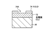
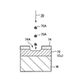
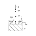
- FIGS. 2A to 2C are process diagrams showing an example of the processing method of the metal film of this embodiment
- FIGS. 2A to 2C are process diagrams showing an example of the processing method of the metal film of this embodiment
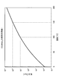
- FIG. 3 is a graph showing a vapor pressure curve of Cu (hfac) 2 which is a reaction byproduct generated when copper is etched. It is.
- the semiconductor wafer W which is an object to be processed, is fixed by the clamper 18 so that the semiconductor wafer W is held on the holding table 16 of the holding means 14 provided in the processing container 4.
- the wafer W is arranged in such a state that the processing surface is directed to the left side in the drawing and faces the gas cluster beam forming means 38.
- 2A to 2C showing the surface of the wafer W in an enlarged manner, first, as shown in FIG. 2A, a metal film 72 to be etched is formed on the surface to be processed which is the surface of the wafer W.
- a mask 74 that is formed in advance and patterned on the surface of the metal film 72 is formed.
- the mask 74 is made of a material resistant to a gas cluster beam, for example, a silicon oxide film (SiO 2) by plasma CVD (Chemical Vapor Deposition). 2 ) or a silicon nitride film (Si 3 N 4 ) is used.
- a silicon oxide film SiO 2 by plasma CVD (Chemical Vapor Deposition). 2
- a silicon nitride film Si 3 N 4
- the inside of the processing container 4 is sealed, and the exhaust system 28 is driven to evacuate the processing container 4 so that the inside of the processing space 6 and The inside of the beam forming space 8 is brought into a high vacuum state.
- the gas cluster beam forming means 38 is driven to generate the gas cluster beam 70. That is, the oxidizing gas, the complex gas, and the rare gas are flowed at a high pressure, and are supplied while the flow rate is controlled. Since the complexing agent that is a raw material of the complexing gas, that is, H (hfac), is a liquid at room temperature, it is pumped while being controlled at a high pressure and is vaporized by the vaporizer 60 to become a complexing gas. This complex gas is mixed and flowed with Ar gas (rare gas) as a carrier gas supplied to the vaporizer 60. The oxidizing gas, complex gas, and rare gas are mixed and supplied to the stay chamber 42 of the injection mechanism 40 through the gas introduction passage 46.
- Ar gas ultraviolet gas
- This mixed gas is in a high pressure state, and this mixed gas is emitted or ejected from the nozzle portion 44 into the beam forming space 8 in a high vacuum state by adiabatic expansion.
- the mixed gas is adiabatically expanded and emitted, and a gas cluster beam 70 is formed and irradiated toward the wafer W.
- the diffused gas cluster is interrupted by the skim plate 10 in the middle, and only the gas cluster beam 70 having high straightness passes through the gas skim hole 12 provided in the skim plate 10 as shown in FIG. 2B.
- the wafer W is irradiated.
- the pressure in the retention chamber 42 is, for example, about 20 atmospheres, and the pressure in the beam forming space 8 and the processing space 6 is a pressure of 10 ⁇ 3 Pa to 105 Pa.
- the gas cluster 70 ⁇ / b> A constituting the gas cluster beam 70 is cooled by the adiabatic expansion of the mixed gas in the nozzle portion 44, and the oxidation gas atom or molecule and the complex gas atom or molecule are centered on the rare gas Ar. It is in a state of being gently restrained. That is, one gas cluster 70A is composed of, for example, several to several thousand atoms or molecules, and an oxidizing gas, a complex gas, and a rare gas are mixed at an atomic level or a molecular level.
- the gas cluster beam 70 When the gas cluster beam 70 is irradiated onto the metal film 72 made of Cu as shown in FIG. 2B, heat is partially generated by the collision energy at this time. At this time, copper and oxidizing gas first react to form an oxide, and this oxide and complexing gas react to form an organometallic complex having a relatively high vapor pressure. As the organometallic complex is gasified and exhausted, the metal film 72 made of Cu is etched as shown in FIGS. 2B and 2C. The metal film 72 exposed in the pattern groove 74 of the mask 74 patterned in this way can be removed by etching with a gas cluster beam.
- the gas cluster beam 70 can be irradiated onto the entire surface of the wafer W and etched. Further, by moving the holding table 16 in the Z direction, the wafer W can be etched toward or away from the injection mechanism 40.
- the reaction between copper, O 2 as an oxidizing gas, and H (hfac) as a complexing gas at the time of etching is expressed as follows.
- the copper oxidized to monovalent or divalent is easily H (hfac) at about 150 ° C. ), It easily becomes locally 150 ° C. or higher due to the collision energy of the gas cluster beam 70, and has a relatively high vapor pressure, that is, a Cu (hfac) 2 complex (organometallic complex) that is easily sublimated. Can be formed.
- FIG. 3 shows a vapor pressure curve of the complex Cu (hfac) 2.
- the vapor pressure is about 100 Torr at a temperature of about 150 ° C.
- the collision energy of the gas cluster beam 70 is converted into thermal energy and easily becomes a temperature of about 150 ° C. microscopically, and the process pressure in the processing space 6 is lower than 100 Torr, for example, so Cu (hfac It can be seen that 2 can be easily sublimated and removed.
- the amount of oxidizing gas contributing to copper oxidation is less than the amount of complexing gas, excess oxidizing gas is eliminated, and side etching as described above occurs. Can be suppressed.
- the amount of the side etching described above can be adjusted and suppressed.
- the amount of the rare gas may be relatively small. For example, an amount of about 1/10 of the oxidizing gas is sufficient, but this flow rate is not particularly limited.
- an oxidizing gas that oxidizes an element of the metal film 72 made of copper to form an oxide for example, a complexing gas that complexes O 2 and the oxide to form an organometallic complex
- a gas cluster beam 70 is formed by adiabatic expansion of a mixed gas of H (hfac) and a rare gas, and the metal cluster film is made to collide with the metal film of the object to be processed, for example, the semiconductor wafer W.
- a metal film that could not be etched by the conventional cluster beam method can be etched by a cluster beam using an oxidizing gas, a complex gas, and a rare gas.
- FIG. 4 is a view showing an example of a processing apparatus according to a modification of the present invention.
- the same components as those shown in FIG. 1 are denoted by the same reference numerals, and the description thereof is omitted.
- a partition wall 80 is provided on the processing space 6 side of the processing container 4 in parallel with the skim plate 10, and an ionization space is provided between the partition wall 80 and the skim plate 10. 82 is formed.
- An irradiation hole 84 having a small hole diameter is formed in the central portion of the partition wall 80 so as to be positioned linearly with the gas skim hole 12 of the skim plate 10 and the nozzle portion 44 of the injection mechanism 40.
- the gas cluster beam 70 is allowed to pass through.
- An exhaust port 86 is also formed at the bottom of the processing container 4 that partitions the ionization space 82, and the exhaust port 86 is connected to the exhaust passage 30 of the exhaust system 28 so that the inside of the ionization space 82 can be evacuated. It is like that.
- an ionizer 88 is provided corresponding to the path through which the gas cluster beam 70 passes, and the gas cluster beam 70 passing through the ionizer 88 is ionized.
- the ionizer 88 for example, an electron impact ionizer having an incandescent filament (not shown) that emits thermal electrons for ionization can be used.
- an accelerating electrode portion 90 for accelerating the ionized gas cluster beam 70 is provided in the downstream path of the ionizer 88.
- the accelerating electrode unit 90 has a plurality of sets of ring-shaped electrodes 92 provided in parallel along the traveling direction of the gas cluster beam 70.
- An acceleration power source (not shown) is connected between the plurality of sets of electrodes 92 to apply a high voltage for beam acceleration.
- the gas cluster beam 70 ionized by the ionizer 88 can be accelerated by the acceleration electrode unit 90 and collide with the wafer W. Accordingly, the metal film can be efficiently etched.
- an oxidizing gas that oxidizes the elements of the metal film to form an oxide and a complexing gas that reacts with the oxide to form an organometallic complex and a rare gas. Since a gas cluster beam is formed by adiabatic expansion of a mixed gas with a gas, and the gas cluster beam collides with the metal film of the object to be processed, the metal film can be etched. Then, the metal film that could not be etched can be etched by a cluster beam using an oxidizing gas, a complex gas, and a rare gas.
- the oxidizing gas includes O 2 , H 2 O, H 2 O 2, and the like.
- H (hfac) which is one of organic acids
- complexing gas complexing agent
- Gases include acetylacetone, hexafluoroacetylacetone (1,1,1,5,5,5-hexafluoro-2,4-pentanedione: H (hfac)), trifluoroacetic acid (TFA), formic acid, acetic acid, propion
- TFA trifluoroacetic acid
- acetic acid acetic acid
- propion One or more materials selected from the group consisting of acid, butyric acid, and valeric acid can be used.
- the case where Ar is used as a rare gas has been described as an example.
- the present invention is not limited to this, and other rare gases such as He, Ne, Kr, and Xe may be used.
- the case where copper is etched as the material of the metal film 72 to be etched has been described as an example.
- the present invention is not limited to this, and the metal film 72 includes Cu, Co, Ni, Pt, and Ru.
- the present invention can also be applied to etching one material selected from the group consisting of:
- the semiconductor wafer is described as an example of the object to be processed.
- the semiconductor wafer of the present invention includes a silicon substrate and a compound semiconductor substrate such as GaAs, SiC, and GaN.
- the present invention is not limited to a substrate, and can also be applied to a glass substrate, a ceramic substrate, or the like used for a liquid crystal display device.
- processing apparatus 4 processing vessel 14 holding means 16 holding base 28 exhaust system 38 gas cluster beam forming means 40 injection mechanism 42 storage chamber 44 nozzle portion 48 oxidizing gas passage 50 complex gas passage 60 vaporizer 62 noble gas passage 70 gas cluster beam 70A gas cluster 72 metal film 74 mask W semiconductor wafer (object to be processed)
Landscapes
- Chemical & Material Sciences (AREA)
- Engineering & Computer Science (AREA)
- Analytical Chemistry (AREA)
- Materials Engineering (AREA)
- Mechanical Engineering (AREA)
- Metallurgy (AREA)
- Organic Chemistry (AREA)
- Chemical Kinetics & Catalysis (AREA)
- General Chemical & Material Sciences (AREA)
- Physics & Mathematics (AREA)
- Plasma & Fusion (AREA)
- Combustion & Propulsion (AREA)
- Drying Of Semiconductors (AREA)
- Internal Circuitry In Semiconductor Integrated Circuit Devices (AREA)
Abstract
被処理体Wの表面に形成された金属膜72をガスクラスタビームにより加工する金属膜の加工方法において、金属膜の元素を酸化して酸化物を形成する酸化ガスと、酸化物と反応して有機金属錯体を形成する錯化ガスと、希ガスとの混合ガスを断熱膨張させてガスクラスタビームを形成し、ガスクラスタビームを被処理体の金属膜に衝突させることにより金属膜をエッチング加工する。
Description
本発明は、半導体ウエハ等の被処理体の表面に形成されている金属膜をガスクラスタビームにより加工する金属膜の加工方法及び加工装置に関する。
超LSIの配線は、現在では銅ダマシン法によって形成されている。銅ダマシン法とは、フォトリソグラフィー技術とドライエッチング技術を用いて絶縁膜にパターン化された溝を形成し、その表面を銅バリア膜で被覆してから銅めっきを溝に埋め込み、不要な上層部をCMP(Chemical Mechanical Polishing)で研磨して除去して金属パターンを形成する方法である(非特許文献1参照)。
銅ダマシン法は、微細な溝に良好に銅バリア膜を被覆するプロセス、銅バリア膜上に良好に銅めっきシード膜を被覆するプロセス、銅めっきを微細構造に良好に埋め込むプロセスが必要とされ、より微細なパターンへの適用が難しくなってきている。さらに、パターン形成にCMPプロセスが必須となるため、TSV(Through Silicon Via)に接続させるバンプのような、大きなパターン形成プロセスにはコスト高になってしまう。
ダマシン法以外の金属膜パターン形成プロセスの一つに、ウエットエッチング法がある。これは金属膜上にマスクをパターニングして、マスクがない金属膜部分を希塩酸などでウエットエッチング除去する手法である。しかし、この手法は金属を等方的にエッチングするため、微細な構造だとサイドエッチング量が制御できずに良好なパターン形成を保つことが難しい。
もう一つの手法として、RIE(Reactive Ion Etching)法がある。この手法は、反応性プラズマによりマスクされていない金属部をエッチングする方法であり、ハロゲン化物の蒸気圧が高い金属元素であるAl、Ti、Ta、WなどをRIE法にてエッチングした場合には、良好なパターン形成が得られることが確認されている(非特許文献2参照)。
しかし、ハロゲン化物の蒸気圧が低い金属であるCo、Ni、Cu,Pt,RuなどをRIE法にてエッチングすることによりパターン形成する場合、ハロゲン化金属をガス化して取り除き、反応容器の壁への再付着を防ぐために基板と反応容器の壁の温度を高温に保つ必要がある。
しかも、このような高温RIEプロセスでは、プラズマの活性種であるハロゲンイオンとラジカルがエッチングにより形成された開口(溝やホール)の側壁を腐食し、良好なパターン形状を保つことが難しい(非特許文献3)。さらには、これらのRIE法では、プラズマで分解されたエッチャントがポリマーや化合物の形で残渣として残り、エッチング後のウエットクリーニングでも除去しきれない問題が頻発する。
一方で、クリーニングやエッチングガスを断熱膨張させることによって発生するガスクラスタビームを用いたクリーニング処理や加工処理が提案されている(特許文献1、2)。この場合、上記ガスクラスタビームをイオン化して加速させることも行われている。そして、上記ガスクラスタビームが材料の表面に衝突すると、その時に発生する熱や化学反応によって表面を清浄化したり、或いは材料をエッチングしたりするようになっている。
D. Edelstein et al, IEDM Technical Digest, IEEE (1997).
Y. Yasuda, Thin Solid Films, Volume 90, Issue 3, 23 April 1982, Pages 259-270.
B.J. Howard and C. Steinbruchel, Applied Physics Letters, 59(8), 19p914, (1991).
上述のようにガスクラスタビームを用いた場合にあっては、シリコン膜に対してエッチング加工を十分に行うことができることが知られている。しかしながら、前述したようなCu、Co、Pt、Ru等の金属により形成される金属ハロゲン化物の蒸気圧はかなり低い。このため、Cu、Co、Pt、Ru等の金属により形成される金属ハロゲン化物に上述したようなガスクラスタビームを衝突させた場合、依然として良好なパターン形成を保つことが難しい、といった問題があった。
以上のような問題点に着目し、本発明の目的とするところは、これを有効に解決すべく創案されたものである。本発明は、従来のクラスタビーム法ではエッチングできなかった金属膜を酸化ガスと錯化ガスと希ガスとを用いたクラスタビームによりエッチングすることが可能な金属膜の加工方法及び加工装置である。
本発明のある態様によれば、前記金属膜の元素を酸化して酸化物を形成する酸化ガスと、前記酸化物と反応して有機金属錯体を形成する錯化ガスと、希ガスとの混合ガスを真空排気が可能な処理容器内にて断熱膨張させてガスクラスタビームを形成する形成ステップと、前記ガスクラスタビームを前記被処理体の表面に形成された金属膜に衝突させることにより前記金属膜をエッチングする加工ステップと、を含む金属膜の加工方法が提供される。
本発明の他の態様によれば、被処理体の表面に形成された金属膜をガスクラスタビームにより加工する金属膜の加工装置において、真空排気が可能になされた処理容器と、前記被処理体を保持する保持手段と、前記保持手段に対向させて設けられると共に、前記金属膜の元素を酸化して酸化物を形成する酸化ガスと前記酸化物と反応して有機金属錯体を形成する錯化ガスと希ガスとの混合ガスを前記処理容器内にて断熱膨張させてガスクラスタビームを形成するガスクラスタビーム形成手段と、を備え、前記ガスクラスタビームを前記被処理体の表面に形成された金属膜に衝突させることにより前記金属膜をエッチングする加工装置が提供される。
本発明によれば、金属膜を酸化ガスと錯化ガスと希ガスとを用いたクラスタビームによりエッチング加工することができる。
以下に、本発明の一実施形態に係る金属膜の加工方法及び加工装置の一例を添付図面に基づいて詳述する。図1は本発明の一実施形態に係る金属膜の加工装置の一例を示す構成図である。本実施形態では金属膜として銅の薄膜に対してパターンニングエッチング加工を施す場合を例にとって説明する。
図1に示すように、この加工装置2は、所定の長さの箱状になされた処理容器4を有している。この処理容器4は、アルミニウム、アルミニウム合金又はステンレススチール等の耐圧性に優れる材料により形成されている。この処理容器2内は、被処理体である例えば半導体ウエハWが設置される処理空間6と、加工のための後述するガスクラスタビームを発生させるビーム形成空間8とに容器内の中央に設けたスキム板10により左右に2つに区分されている。このスキム板10の中央部には、直進性の高いガスクラスタビームのみを通過させるガススキム孔12が形成されている。
このガススキム孔12の開口面積は非常に小さいが、このガススキム孔12を介して上記処理空間6とビーム形成空間8とは連通状態になされている。そして、上記処理空間6内には、上記半導体ウエハWを保持する保持手段14が設けられている。具体的には、この保持手段14は、ウエハWを保持するために例えば円板状になされた保持台16を有している。この保持台16を上下方向に起立させて設け、この一側面にウエハWの裏面を当接させて、ウエハWの周辺部をクランパ18により固定するようになっている。この保持台16は、処理容器4の天井部に設けた走査アクチュエータ20により支持されている。
具体的には、この走査アクチュエータ20は、下方に延びるアーム22を有しており、このアーム22に上記保持台16を取り付け固定している。このアーム22は、図中において上下方向[Y方向]、左右方向[Z方向]及び紙面の垂直方向[X方向](図示せず)へそれぞれ移動可能になされている。X方向及びY方向へは、ウエハWの少なくとも半径の長さだけ走査移動できるようになっており、この走査移動により図中左側から直進してくることになるガスクラスタビームをウエハWの全面に照射できるようになっている。
また、上記処理空間6及びビーム形成空間8を区画する処理容器4の各底部には、それぞれ排気口24、26が設けられており、各排気口24、26には、真空引きを行う排気系28が接続されている。具体的には、この排気系28は、上記2つの排気口24、26に共通に接続された排気通路30を有している。そして、この排気通路30にその上流側より下流側に向けて圧力調整を行うための圧力調整弁32と第1の真空ポンプ34と第2の真空ポンプ36が順次介設されており、上記処理容器4内の全体を圧力調整して高真空状態に維持できるようになっている。上記第1の真空ポンプ34として例えばターボ分子ポンプが用いられ、上記第2の真空ポンプ36としては例えばドライポンプが用いられる。
そして、この処理容器4内には、上記保持台16に対向させるようにしてガスクラスタビーム形成手段38が設けられている。具体的には、このガスクラスタビーム形成手段38は、ガスクラスタを高速で噴射する噴射機構40を有している。この噴射機構40は、ある程度の大きさの容量になされた横長の滞留チャンバ42と、この横長の滞留チャンバ42の先端側に設けられて噴射方向に向けて次第に拡径されたラッパ状のノズル部44とよりなり、全体として例えばラバールノズルを構成している。
そして、この滞留チャンバ42には、ガスクラスタビームの形成に必要な各種のガスを導入するためのガス導入通路46が接続されている。このガス導入通路46には、酸化ガスを流す酸化ガス通路48と錯化ガスを流す錯化ガス通路50とが共通に接続される。そして、上記酸化ガス通路48には、その上流側より下流側に向けてマスフローコントローラのような気体用の流量制御器52及び開閉弁54が順次介設されており、高い圧力の酸化ガスを流量制御しつつ供給できるようになっている。ここで酸化ガスとして例えばO2(酸素)が用いられる。
本実施形態では、室温で液体の錯化剤が用いられる。このため、上記錯化ガス通路50には、その上流側より下流側に向けて液体用マスフローコントローラのような流量制御器56、開閉弁58及び気化器60が順次介設されている。そして、上記気化器60には、キャリアガスとして機能する希ガスを流すための希ガス通路62が接続される。そして、この希ガス通路62は、その上流側より下流側に向けてマスフローコントローラのような気体用の流量制御器64及び開閉弁66が順次介設されており、高い圧力の希ガスをキャリアガスとして流量制御しつつ供給できるようになっている。
ここでは上記錯化剤として室温で液体のヘキサフルオロアセチルアセトン(1,1,1,5,5,5-Hexafluoro-2,4-pentanedione:H(hfac))が用いられ、また、キャリアガスとなる希ガスとしてはArが用いられる。上記液体の錯化剤は高い圧力で圧送されて流され、気化器60にて気化されて錯化ガスとなり、高い圧力のキャリアガス(Ar)との混合状態となって下流に向けて流れるようになっている。
そして、酸化ガス、錯化ガス及び希ガス(キャリアガス)は混合状態となってガス導入通路46から高圧状態のまま滞留チャンバ42へ導入され、この先端のノズル部44より真空状態のビーム形成空間8に向けて断熱膨張させることにより、ガスクラスタビーム70を形成し得るようになっている。この場合、上記噴射機構40は、ノズル部44とガススキマ孔12の開口部の中央が同じ高さに位置し、噴射されるガスクラスタビーム70の中心がガススキマ孔12を通過するように設置される。ここで上記酸化ガスは半導体ウエハWの表面に形成されている金属膜の元素を酸化して酸化物を形成する作用を有す。また、上記錯化ガスは上記酸化物と反応して有機金属錯体を形成する作用を有す。また、上記希ガスはガスクラスタを形成する際の核となる作用を有している。
尚、ここでは酸化ガスと錯化ガス(キャリアガスを含む)とを通路の途中で混合させたが、これに限定されず、これらの両ガスを別々に滞留チャンバ42に導入して滞留チャンバ42内で混合ガスを形成するようにしてもよい。また、錯化ガスに対して希ガスのキャリアガスが不要な場合には、希ガスを通路途中で酸化ガスや錯化ガスと混合させて混合ガスを形成したり、或いは希ガスを直接的に滞留チャンバ42内へ導入して混合ガスを形成するようにしてもよい。
以上のように構成された加工装置2の全体の動作は、例えばコンピュータ等よりなる装置制御部72により制御されるようになっており、この動作を行うコンピュータのプログラムは、記憶媒体74に記憶されている。この記憶媒体74は、例えばフレキシブルディスク、CD(CompactDisc)、ハードディスク、フラッシュメモリ或いはDVD等よりなる。具体的には、この装置制御部72からの指令により、各種のガスの供給の開始、停止や流量制御、プロセス圧力の制御等が行われる。
また、上記装置制御部72は、装置制御部72とオペレータにより操作される装置とを接続するユーザインターフェース(図示せず)を有しており、ユーザインターフェースはオペレータが装置を管理するためにコマンドの入出力操作等を行なうキーボードや、装置の稼働状況を可視化して表示するディスプレイ等であってもよい。更に、装置制御部72は通信回線(図示せず)に接続され、通信回線を介して上記各制御のための情報の通信を上記装置制御部72に対して行なうようにしてもよい。
<加工方法>
次に、以上のように構成された加工装置2を用いて行われる本実施形態の金属膜の加工方法について、図1~図3を参照して説明する。図2A~図2Cは本実施形態の金属膜の加工方法の一例を示す工程図、図3は銅をエッチングする時に発生する反応副生成物であるCu(hfac)2の蒸気圧曲線を示すグラフである。
<加工方法>
次に、以上のように構成された加工装置2を用いて行われる本実施形態の金属膜の加工方法について、図1~図3を参照して説明する。図2A~図2Cは本実施形態の金属膜の加工方法の一例を示す工程図、図3は銅をエッチングする時に発生する反応副生成物であるCu(hfac)2の蒸気圧曲線を示すグラフである。
まず、被処理体である半導体ウエハWをクランパ18により固定することにより、半導体ウエハWを処理容器4内に設けた保持手段14の保持台16上に保持する。この時、ウエハWは被加工面が図中左側に向いており、ガスクラスタビーム形成手段38に向けて対向するような状態で配置する。ウエハWの表面を拡大して示した図2A~図2Cを参照すると、まず、図2Aに示すように、このウエハWの表面である被加工面にはエッチングの加工対象となる金属膜72が予め形成されており、この金属膜72の表面にパターン化されたマスク74が形成されている。ここでは前述したように、上記金属膜として銅(Cu)が用いられ、また上記マスク74としてはガスクラスタビームに対して耐性のある材料、例えばプラズマCVD(Chemical Vapor Deposition)によるシリコン酸化膜(SiO2)やシリコン窒化膜(Si3N4)が用いられる。
さて、上述のようにウエハWを保持台16に保持させたならば、この処理容器4内を密閉すると共に、排気系28を駆動して処理容器4内を真空引きし、処理空間6内及びビーム形成空間8内を高真空状態にする。
そして、ガスクラスタビーム形成手段38を駆動させてガスクラスタビーム70を発生させる。すなわち、酸化ガスと錯化ガスと希ガスとがそれぞれ高い圧力で流されてきて、それぞれ流量制御されつつ供給される。錯化ガスの原料である錯化剤、すなわちH(hfac)は室温で液体なので、高い圧力で流量制御されつつ圧送され、気化器60にて気化されて錯化ガスとなる。この錯化ガスは気化器60に供給されるキャリアガスとしてのArガス(希ガス)と混合されて流される。そして、上記酸化ガスと錯化ガスと希ガスとは混合ガスとなってガス導入通路46を通り、噴射機構40の滞留チャンバ42内へ供給される。この混合ガスは高圧状態になっており、この混合ガスはノズル部44から高真空状態になっているビーム形成空間8内に向けて断熱膨張により放射乃至噴射される。この時、処理容器4内は高真空状態になっているため、混合ガスは断熱膨張して放射され、ガスクラスタビーム70が形成されてウエハWに向けて照射されることになる。
このガスクラスタビーム70は、拡散したガスクラスタは途中にスキム板10で遮断され、スキム板10に設けたガススキム孔12を直進性の高いガスクラスタビーム70のみが通過して、図2Bに示すようにウエハWに照射される。上記滞留チャンバ42内の圧力は、例えば20気圧程度であり、ビーム形成空間8内及び処理空間6内の圧力は10-3Pa以上で105Pa以下の圧力である。
上記ガスクラスタビーム70を構成するガスクラスタ70Aは、先のノズル部44における混合ガスの断熱膨張による冷却により、希ガスであるArを核として酸化ガスの原子或いは分子と錯化ガスの原子或いは分子と緩やかに束縛された状態となっている。すなわち、1つのガスクラスタ70Aは、例えば数個~数千個の原子、又は分子からなり、酸化ガスと錯化ガスと希ガスとが原子レベル或いは分子レベルで混在した状態となっている。
上記ガスクラスタビーム70が図2Bに示すようにCuよりなる金属膜72に照射されると、この時の衝突エネルギーによって部分的に熱が発生する。この時、まず銅と酸化ガスとが反応して酸化物が形成され、この酸化物と錯化ガスとが反応して比較的蒸気圧の高い有機金属錯体が形成される。この有機金属錯体がガス化して排気されていくことにより、Cuよりなる金属膜72が図2B及び図2Cに示すようにエッチングされることになる。このようにしてパターン化されたマスク74のパターン溝74内に露出している金属膜72をガスクラスタビームによるエッチングにより除去することができる。
また、走査アクチュエータ20により保持台16をX方向及びY方向へ走査することにより、ガスクラスタビーム70をウエハWの全面へ照射させてエッチングすることができる。また、Z方向へ保持台16を移動させることによってウエハWを噴射機構40に対して接近、或いは離間させてエッチングすることができる。このエッチング時の銅と酸化ガスであるO2と錯化ガスであるH(hfac)との反応は次のように表される。
4Cu+O2→2Cu2O(Cu:1価)
2Cu+O2→2CuO(Cu:2価)
Cu2O+2H(hfac)→Cu+Cu(hfac)2↑+H2O↑
CuO+2H(hfac)→Cu(hfac)2↑+H2O↑
ここで矢印↑はガスとなって飛散して行くことを示す。反応副生成物として形成される有機金属錯体である錯体Cu(hfac)2は比較的蒸気圧が高いので容易に昇華させて取り除くことができる。ここで酸化していない銅は、少なくとも265℃以上でなければH(hfac)と反応しないが、上述したように1価又は2価に酸化されている銅は150℃程度で容易にH(hfac)と反応するので、ガスクラスタビーム70の衝突エネルギーで局所的に容易に150℃以上になり、これより蒸気圧の比較的高い、すなわち昇華し易いCu(hfac)2なる錯体(有機金属錯体)を形成することができる。
4Cu+O2→2Cu2O(Cu:1価)
2Cu+O2→2CuO(Cu:2価)
Cu2O+2H(hfac)→Cu+Cu(hfac)2↑+H2O↑
CuO+2H(hfac)→Cu(hfac)2↑+H2O↑
ここで矢印↑はガスとなって飛散して行くことを示す。反応副生成物として形成される有機金属錯体である錯体Cu(hfac)2は比較的蒸気圧が高いので容易に昇華させて取り除くことができる。ここで酸化していない銅は、少なくとも265℃以上でなければH(hfac)と反応しないが、上述したように1価又は2価に酸化されている銅は150℃程度で容易にH(hfac)と反応するので、ガスクラスタビーム70の衝突エネルギーで局所的に容易に150℃以上になり、これより蒸気圧の比較的高い、すなわち昇華し易いCu(hfac)2なる錯体(有機金属錯体)を形成することができる。
この錯体は、上述のように蒸気圧が比較的高いので、ウエハW自体を高温に加熱しなくても容易に昇華して除去されることになる。図3は錯体Cu(hfac)2の蒸気圧曲線を示しており、例えば温度150℃程度で蒸気圧は100Torr程度である。従って、ガスクラスタビーム70の衝突エネルギーは熱エネルギーに変換されて微視的に容易に150℃程度の温度になり、しかも処理空間6内のプロセス圧力は、例えば100Torrよりも低いので、Cu(hfac)2を容易に昇華させて除去できることが判る。
また、上述のようにガスクラスタビーム70がCuの金属膜72に最初に衝突した時にその衝突面でCuとの酸化反応により酸化ガスであるO2がほとんど消費されてしまうので、衝突面より周囲に散乱された分子中にはほとんど酸素が含まれていない。仮に未反応のO2が存在しても二次的な散乱で運動エネルギーを失っているので、側壁に衝突しても酸化反応を起こしにくい。このため、散乱された分子によって2次的なエッチングが行われる確立が非常に小さくなってサイドエッチングが抑制され、結果的に金属エッチング溝の側壁の形状を平滑に保つことができる。
この場合、特に、銅の酸化に寄与する酸化ガスの量を錯化ガスの量よりも少なく設定しておくことにより過剰な酸化ガスがなくなって、上述のようなサイドエッチングが発生することを一層抑制することができる。このサイドエッチングの抑制効果を十分に発揮させるには、錯化ガスの量を酸化ガスの量の5倍以上の大きさに設定しておくのが好ましい。特に、上記酸化ガスの量と錯化ガスの量の比とを適宜コントロールすることにより、上記したサイドエッチングの発生量も調整し、且つ抑制することができる。また希ガスの量は比較的少なくてよく、例えば酸化ガスの1/10程度の量で十分であるが、この流量は特に限定されるものではない。
このように、本実施形態では例えば銅よりなる金属膜72の元素を酸化して酸化物を形成する酸化ガス、例えばO2と上記酸化物を錯化して有機金属錯体を形成する錯化ガス、例えばH(hfac)と希ガスとの混合ガスを断熱膨張させてガスクラスタビーム70を形成し、上記ガスクラスタビームを上記被処理体、例えば半導体ウエハWの金属膜に衝突させることにより上記金属膜をエッチングするようにしたので、従来のクラスタビーム法ではエッチングできなかった金属膜を酸化ガスと錯化ガスと希ガスとを用いたクラスタビームによりエッチング加工することができる。
<変形例>
次に本発明の変形例に係る加工装置について説明する。先の実施形態ではガスクラスタビーム形成手段38により形成したガスクラスタビーム70を直接的に半導体ウエハWに衝突させたが、これに限定されず、このガスクラスタビーム70を途中でイオン化させると共に速度を更に加速してウエハに衝突させるようにしてもよい。このような加工装置の変形例は図4に示される。
<変形例>
次に本発明の変形例に係る加工装置について説明する。先の実施形態ではガスクラスタビーム形成手段38により形成したガスクラスタビーム70を直接的に半導体ウエハWに衝突させたが、これに限定されず、このガスクラスタビーム70を途中でイオン化させると共に速度を更に加速してウエハに衝突させるようにしてもよい。このような加工装置の変形例は図4に示される。
図4は本発明の変形例に係る加工装置の一例を示す図である。尚、図4中において、図1中に示す構成部分と同一構成部分については同一参照符号を付してその説明を省略する。図4に示すように、この加速装置では、処理容器4の処理空間6側に、スキム板10と平行に区画壁80を設けて、この区画壁80と上記スキム板10との間にイオン化空間82を形成している。
そして、この区画壁80の中央部には、上記スキム板10のガススキム孔12及び噴射機構40のノズル部44と直線上に位置するように小さな穴径の照射孔84が形成されており、ここにガスクラスタビーム70を通過させるようになっている。そして、このイオン化空間82を区画する処理容器4の底部にも排気口86が形成されており、この排気口86は排気系28の排気通路30に接続されて、イオン化空間82内を真空引きできるようになっている。
そして、イオン化空間82内には、ガスクラスタビーム70が通過する経路に対応させてイオナイザ88が設けられており、このイオナイザ88内を通過するガスクラスタビーム70をイオン化するようになっている。このイオナイザ88としては、例えばイオン化のための熱電子を放出する白熱フィラメント(図示せず)を有する電子衝突イオナイザを用いることができる。
このイオナイザ88の下流側の経路には、上記イオン化されたガスクラスタビーム70を加速させる加速電極部90が設けられている。この加速電極部90は、ガスクラスタビーム70の進行方向に沿って並列させて設けた複数組のリング状の電極92を有している。そして、この複数組の電極92間に加速電源(図示せず)を接続してビーム加速用の高電圧を印加するようになっている。
この変形によれば、先の実施形態と同様な作用効果を発揮できるのみならず、イオナイザ88でイオン化したガスクラスタビーム70を加速電極部90で加速してウエハWに衝突させることができるので、その分、効率的に金属膜のエッチング加工を行うことができる。
以上、上記実施形態及び変形例に係る金属膜の加工方法及び加工装置によれば、次のように優れた作用効果を発揮することができる。
非プラズマプロセスなので、ハロゲンラジカルやイオンによる側壁表面の腐食がない。よって、RIE法と比較して良好なエッチング形状を得られる。同様に、プラズマで活性化したエッチングガスがポリマー化してマスク表面やエッチング側壁に堆積することがない。このため、エッチング後の加工基板の洗浄工程が大幅に簡易化される。
導入したガスから蒸気圧が高い有機金属錯体が形成され、排気されるため、処理容器側壁への副生成物付着量を劇的に低減できる。そのため、装置処理容器の内壁クリーニング回数を低減できて、装置の使用効率を高く保つことが出来る。
被処理体の表面に形成された金属膜を加工するに際して、金属膜の元素を酸化して酸化物を形成する酸化ガスと上記酸化物と反応して有機金属錯体を形成する錯化ガスと希ガスとの混合ガスを断熱膨張させてガスクラスタビームを形成し、上記ガスクラスタビームを上記被処理体の金属膜に衝突させることにより上記金属膜をエッチングできるようにしたので、従来のクラスタビーム法ではエッチングできなかった金属膜を酸化ガスと錯化ガスと希ガスとを用いたクラスタビームによりエッチング加工することができる。
以上、添付図面を参照しながら本発明の好適な実施形態について詳細に説明したが、本発明はかかる例に限定されない。本発明の属する技術の分野における通常の知識を有する者であれば、特許請求の範囲に記載された技術的思想の範疇において、各種の変更例または修正例に想到し得ることは明らかであり、これらについても、当然に本発明の技術的範囲に属するものと了解される。
例えば以上の実施形態では、酸化ガスとしてO2ガスを用いた場合を例にとって説明したが、本発明はこれに限定されず、酸化ガスとしては、O2とH2OとH2O2とよりなる群から選択される1以上の材料を用いることができる。
また、以上の実施形態では、錯化ガス(錯化剤)として有機酸の1つであるH(hfac)を用いた場合を例にとって説明したが、本発明はこれに限定されず、錯化ガスとしては、アセチルアセトン、ヘキサフルオロアセチルアセトン(1,1,1,5,5,5-Hexafluoro-2,4-pentanedione:H(hfac))、トリフルオロ酢酸(trifluoroaceticacid:TFA)、蟻酸、酢酸、プロピオン酸、酪酸、及び吉草酸とよりなる群から選択される1以上の材料を用いることができる。
また以上の実施形態では、希ガスとしてArを用いた場合を例にとって説明したが、本発明はこれに限定されず、He、Ne、Kr、Xe等の他の希ガスを用いてもよい。また以上の実施形態では、エッチングされる金属膜72の材料として銅をエッチングする場合を例にとって説明したが、本発明はこれに限定されず、金属膜72としてCuとCoとNiとPtとRuとよりなる群から選択される1の材料をエッチングする場合にも本発明を適用することができる。
また、上記実施形態では被処理体として半導体ウエハを例にとって説明したが、本発明の半導体ウエハにはシリコン基板やGaAs、SiC、GaNなどの化合物半導体基板も含まれ、更に、本発明はこれらの基板に限定されず、液晶表示装置に用いるガラス基板やセラミック基板等にも適用することができる。
本国際出願は、2011年1月25日に出願された日本国特許出願2011-013313号に基づく優先権を主張するものであり、その全内容を本国際出願に援用する。
2加工装置
4処理容器
14保持手段
16保持台
28排気系
38ガスクラスタビーム形成手段
40噴射機構
42貯留チャンバ
44ノズル部
48酸化ガス通路
50錯化ガス通路
60気化器
62希ガス通路
70ガスクラスタビーム
70Aガスクラスタ
72金属膜
74マスク
W半導体ウエハ(被処理体)
4処理容器
14保持手段
16保持台
28排気系
38ガスクラスタビーム形成手段
40噴射機構
42貯留チャンバ
44ノズル部
48酸化ガス通路
50錯化ガス通路
60気化器
62希ガス通路
70ガスクラスタビーム
70Aガスクラスタ
72金属膜
74マスク
W半導体ウエハ(被処理体)
Claims (16)
- 前記金属膜の元素を酸化して酸化物を形成する酸化ガスと、前記酸化物と反応して有機金属錯体を形成する錯化ガスと、希ガスとの混合ガスを真空排気が可能な処理容器内にて断熱膨張させてガスクラスタビームを形成する形成ステップと、
前記ガスクラスタビームを前記被処理体の表面に形成された金属膜に衝突させることにより前記金属膜をエッチングする加工ステップと、
を含む金属膜の加工方法。 - 前記酸化ガスは、O2とH2OとH2O2の群から選択される1以上の材料よりなることを特徴とする請求項1記載の金属膜の加工方法。
- 前記錯化ガスは、アセチルアセトン、ヘキサフルオロアセチルアセトン(1,1,1,5,5,5-Hexafluoro-2,4-pentanedione:H(hfac))、トリフルオロ酢酸(trifluoroaceticacid:TFA)、蟻酸、酢酸、プロピオン酸、酪酸、及び吉草酸の群から選択される1以上の材料よりなることを特徴とする請求項1の金属膜の加工方法。
- 前記加工ステップは、ガスクラスタビームをイオン化し、加速して金属膜に衝突させる請求項1に記載の金属膜の加工方法。
- 前記形成ステップは、前記酸化ガスの量を前記錯化ガスの量よりも少なく設定した混合ガスからガスクラスタビームを形成する請求項1に記載の金属膜の加工方法。
- 前記加工ステップは、前記金属膜の表面に形成された、パターン化されたマスクを用いて前記金属膜を加工する請求項1に記載の金属膜の加工方法。
- 前記金属膜は、CuとCoとNiとPtとRuの群から選択される1の材料よりなる請求項1に記載の金属膜の加工方法。
- 真空排気が可能な処理容器と、
前記被処理体を保持する保持手段と、
前記保持手段に対向させて設けられると共に、前記金属膜の元素を酸化して酸化物を形成する酸化ガスと、前記酸化物と反応して有機金属錯体を形成する錯化ガスと、希ガスとの混合ガスを前記処理容器内にて断熱膨張させてガスクラスタビームを形成するガスクラスタビーム形成手段と、
を備え、
前記ガスクラスタビームを前記被処理体の表面に形成された金属膜に衝突させることにより前記金属膜をエッチングする加工装置。 - 更に、前記ガスクラスタビーム形成手段から前記ガスクラスタビームを放射するノズル部と、該ノズル部に対向配置され、前記保持手段により保持された被処理体との間に、前記ガスクラスタビームから所望の方向に向かうビームのみを選択して通過させるガススキム孔を有するスキム板を備えた請求項8記載の加工装置。
- 更に、前記ガスクラスタビームをイオン化するイオナイザと、
イオン化された前記ガスクラスタビームを加速させる加速電極部と、
を備えたことを特徴とする請求項8記載の加工装置。 - 更に、前記スキム板と被処理体との間に前記スキム板に平行に設けられた区画壁を備え、
前記イオナイザと前記加速電極部とは、前記区画壁と前記スキム板とにより仕切られたイオン化空間に配置され、前記イオン化空間にてイオン化され、加速された前記ガスクラスタビームを前記区画壁に設けられた照射孔から被処理体に照射させる請求項10記載の加工装置。 - 前記酸化ガスは、O2とH2OとH2O2の群から選択される1以上の材料よりなることを特徴とする請求項8に記載の加工装置。
- 前記錯化ガスは、アセチルアセトン、ヘキサフルオロアセチルアセトン(1,1,1,5,5,5-Hexafluoro-2,4-pentanedione:H(hfac))、トリフルオロ酢酸(trifluoroaceticacid:TFA)、蟻酸、酢酸、プロピオン酸、酪酸、及び吉草酸の群から選択される1以上の材料よりなることを特徴とする請求項8に記載の加工装置。
- 前記ガスクラスタビーム形成手段は、前記酸化ガスの量を前記錯化ガスの量よりも少なく設定した混合ガスからガスクラスタビームを形成する請求項8に記載の加工装置。
- 前記加工装置は、前記金属膜の表面に形成された、パターン化されたマスクを用いて前記金属膜を加工する請求項8に記載の加工装置。
- 前記金属膜は、CuとCoとNiとPtとRuの群から選択される1の材料よりなることを特徴とする請求項8に記載の加工装置。
Priority Applications (3)
| Application Number | Priority Date | Filing Date | Title |
|---|---|---|---|
| KR1020137019681A KR20140016884A (ko) | 2011-01-25 | 2012-01-17 | 금속막의 가공 방법 및 가공 장치 |
| CN2012800038506A CN103229278A (zh) | 2011-01-25 | 2012-01-17 | 金属膜的加工方法及加工装置 |
| US13/950,658 US20130306597A1 (en) | 2011-01-25 | 2013-07-25 | Processing apparatus and method for processing metal film |
Applications Claiming Priority (2)
| Application Number | Priority Date | Filing Date | Title |
|---|---|---|---|
| JP2011013313A JP5811540B2 (ja) | 2011-01-25 | 2011-01-25 | 金属膜の加工方法及び加工装置 |
| JP2011-013313 | 2011-01-25 |
Related Child Applications (1)
| Application Number | Title | Priority Date | Filing Date |
|---|---|---|---|
| US13/950,658 Continuation US20130306597A1 (en) | 2011-01-25 | 2013-07-25 | Processing apparatus and method for processing metal film |
Publications (1)
| Publication Number | Publication Date |
|---|---|
| WO2012102139A1 true WO2012102139A1 (ja) | 2012-08-02 |
Family
ID=46580711
Family Applications (1)
| Application Number | Title | Priority Date | Filing Date |
|---|---|---|---|
| PCT/JP2012/050869 Ceased WO2012102139A1 (ja) | 2011-01-25 | 2012-01-17 | 金属膜の加工方法及び加工装置 |
Country Status (6)
| Country | Link |
|---|---|
| US (1) | US20130306597A1 (ja) |
| JP (1) | JP5811540B2 (ja) |
| KR (1) | KR20140016884A (ja) |
| CN (1) | CN103229278A (ja) |
| TW (1) | TW201250807A (ja) |
| WO (1) | WO2012102139A1 (ja) |
Cited By (1)
| Publication number | Priority date | Publication date | Assignee | Title |
|---|---|---|---|---|
| CN111771262A (zh) * | 2019-02-01 | 2020-10-13 | 株式会社日立高新技术 | 蚀刻方法以及等离子处理装置 |
Families Citing this family (16)
| Publication number | Priority date | Publication date | Assignee | Title |
|---|---|---|---|---|
| JP6142676B2 (ja) * | 2013-05-31 | 2017-06-07 | セントラル硝子株式会社 | ドライエッチング方法、ドライエッチング装置、金属膜及びそれを備えたデバイス |
| US10147613B2 (en) * | 2014-06-30 | 2018-12-04 | Tokyo Electron Limited | Neutral beam etching of Cu-containing layers in an organic compound gas environment |
| US9735019B2 (en) | 2014-09-05 | 2017-08-15 | Tel Epion Inc. | Process gas enhancement for beam treatment of a substrate |
| JP6545053B2 (ja) * | 2015-03-30 | 2019-07-17 | 東京エレクトロン株式会社 | 処理装置および処理方法、ならびにガスクラスター発生装置および発生方法 |
| KR102437717B1 (ko) * | 2015-06-17 | 2022-08-29 | 인텔 코포레이션 | 디바이스 제조를 위한 산화물 층들의 원자 층 제거에 의한 전이 금속 건식 에칭 |
| JP6529371B2 (ja) * | 2015-07-27 | 2019-06-12 | 東京エレクトロン株式会社 | エッチング方法及びエッチング装置 |
| DE112016004214T5 (de) * | 2015-09-16 | 2018-07-26 | Tel Epion Inc. | Verfahren für hohen Durchsatz unter Verwendung von Strahl-Scangröße und Strahlen-Position in einem Strahlen-Bearbeitungssystem |
| JP2017084965A (ja) * | 2015-10-28 | 2017-05-18 | 東京エレクトロン株式会社 | 遷移金属膜のエッチング方法及び基板処理装置 |
| FR3046801B1 (fr) * | 2016-01-19 | 2020-01-17 | Kobus Sas | Procede d'elimination d'un depot metallique dispose sur une surface dans une enceinte |
| KR102342124B1 (ko) * | 2019-02-14 | 2021-12-22 | 주식회사 히타치하이테크 | 반도체 제조 장치 |
| JP6854844B2 (ja) * | 2019-05-08 | 2021-04-07 | 東京エレクトロン株式会社 | エッチング方法及びエッチング装置 |
| JP7334259B2 (ja) * | 2019-11-01 | 2023-08-28 | 東京エレクトロン株式会社 | 基板洗浄装置および基板洗浄方法 |
| US20230027528A1 (en) * | 2020-12-10 | 2023-01-26 | Hitachi High-Tech Corporation | Semiconductor manufacturing method and semiconductor manufacturing apparatus |
| JP7307861B2 (ja) * | 2021-06-09 | 2023-07-12 | 株式会社日立ハイテク | 半導体製造方法及び半導体製造装置 |
| JP2025113729A (ja) * | 2024-01-23 | 2025-08-04 | 日本電子株式会社 | 集束イオンビーム装置 |
| US20260018422A1 (en) * | 2024-07-12 | 2026-01-15 | Tokyo Electron Limited | Method processing metal features in a semiconductor substrate |
Citations (4)
| Publication number | Priority date | Publication date | Assignee | Title |
|---|---|---|---|---|
| JP2003532349A (ja) * | 2000-05-02 | 2003-10-28 | エピオン コーポレイション | Gcib処理によるデバイス特性の調整システム及び方法 |
| JP2005512312A (ja) * | 2001-10-11 | 2005-04-28 | エピオン コーポレイション | 相互接続バイアを改善するためのgcib処理および改善された相互接続バイア |
| JP2009043975A (ja) * | 2007-08-09 | 2009-02-26 | Tokyo Electron Ltd | ドライクリーニング方法、基板処理装置、半導体装置の製造方法及び記憶媒体 |
| JP2010027788A (ja) * | 2008-07-17 | 2010-02-04 | Tokyo Electron Ltd | 銅の異方性ドライエッチング方法および装置 |
Family Cites Families (16)
| Publication number | Priority date | Publication date | Assignee | Title |
|---|---|---|---|---|
| US5736002A (en) * | 1994-08-22 | 1998-04-07 | Sharp Microelectronics Technology, Inc. | Methods and equipment for anisotropic, patterned conversion of copper into selectively removable compounds and for removal of same |
| US5705443A (en) * | 1995-05-30 | 1998-01-06 | Advanced Technology Materials, Inc. | Etching method for refractory materials |
| US6159859A (en) * | 1998-06-09 | 2000-12-12 | Air Products And Chemicals, Inc. | Gas phase removal of SiO2 /metals from silicon |
| US6375790B1 (en) * | 1999-07-19 | 2002-04-23 | Epion Corporation | Adaptive GCIB for smoothing surfaces |
| WO2003019629A2 (en) * | 2001-08-27 | 2003-03-06 | Nptest, Inc. | Process for charged particle beam micro-machining of copper |
| US7115511B2 (en) * | 2002-11-08 | 2006-10-03 | Epion Corporation | GCIB processing of integrated circuit interconnect structures |
| US20070010095A1 (en) * | 2003-05-28 | 2007-01-11 | Kyoto University | Surface treatment method using ion beam and surface treating device |
| US7405152B2 (en) * | 2005-01-31 | 2008-07-29 | International Business Machines Corporation | Reducing wire erosion during damascene processing |
| JP2007066794A (ja) * | 2005-09-01 | 2007-03-15 | Canon Inc | ガスクラスターイオンビーム装置 |
| US7709344B2 (en) * | 2005-11-22 | 2010-05-04 | International Business Machines Corporation | Integrated circuit fabrication process using gas cluster ion beam etching |
| JPWO2007123102A1 (ja) * | 2006-04-18 | 2009-09-03 | 株式会社アルバック | 成膜装置、バリア膜製造方法 |
| US7670964B2 (en) * | 2007-03-22 | 2010-03-02 | Tokyo Electron Limited | Apparatus and methods of forming a gas cluster ion beam using a low-pressure source |
| US7626183B2 (en) * | 2007-09-05 | 2009-12-01 | Tel Epion Inc. | Methods for modifying features of a workpiece using a gas cluster ion beam |
| US8313663B2 (en) * | 2008-09-24 | 2012-11-20 | Tel Epion Inc. | Surface profile adjustment using gas cluster ion beam processing |
| US8187971B2 (en) * | 2009-11-16 | 2012-05-29 | Tel Epion Inc. | Method to alter silicide properties using GCIB treatment |
| US8512586B2 (en) * | 2011-09-01 | 2013-08-20 | Tel Epion Inc. | Gas cluster ion beam etching process for achieving target etch process metrics for multiple materials |
-
2011
- 2011-01-25 JP JP2011013313A patent/JP5811540B2/ja not_active Expired - Fee Related
-
2012
- 2012-01-17 KR KR1020137019681A patent/KR20140016884A/ko not_active Withdrawn
- 2012-01-17 CN CN2012800038506A patent/CN103229278A/zh active Pending
- 2012-01-17 WO PCT/JP2012/050869 patent/WO2012102139A1/ja not_active Ceased
- 2012-01-20 TW TW101102703A patent/TW201250807A/zh unknown
-
2013
- 2013-07-25 US US13/950,658 patent/US20130306597A1/en not_active Abandoned
Patent Citations (4)
| Publication number | Priority date | Publication date | Assignee | Title |
|---|---|---|---|---|
| JP2003532349A (ja) * | 2000-05-02 | 2003-10-28 | エピオン コーポレイション | Gcib処理によるデバイス特性の調整システム及び方法 |
| JP2005512312A (ja) * | 2001-10-11 | 2005-04-28 | エピオン コーポレイション | 相互接続バイアを改善するためのgcib処理および改善された相互接続バイア |
| JP2009043975A (ja) * | 2007-08-09 | 2009-02-26 | Tokyo Electron Ltd | ドライクリーニング方法、基板処理装置、半導体装置の製造方法及び記憶媒体 |
| JP2010027788A (ja) * | 2008-07-17 | 2010-02-04 | Tokyo Electron Ltd | 銅の異方性ドライエッチング方法および装置 |
Cited By (2)
| Publication number | Priority date | Publication date | Assignee | Title |
|---|---|---|---|---|
| CN111771262A (zh) * | 2019-02-01 | 2020-10-13 | 株式会社日立高新技术 | 蚀刻方法以及等离子处理装置 |
| CN111771262B (zh) * | 2019-02-01 | 2023-12-08 | 株式会社日立高新技术 | 蚀刻方法以及等离子处理装置 |
Also Published As
| Publication number | Publication date |
|---|---|
| KR20140016884A (ko) | 2014-02-10 |
| JP5811540B2 (ja) | 2015-11-11 |
| TW201250807A (en) | 2012-12-16 |
| CN103229278A (zh) | 2013-07-31 |
| JP2012156259A (ja) | 2012-08-16 |
| US20130306597A1 (en) | 2013-11-21 |
Similar Documents
| Publication | Publication Date | Title |
|---|---|---|
| JP5811540B2 (ja) | 金属膜の加工方法及び加工装置 | |
| TWI556305B (zh) | 透過介穩氫終止之矽的選擇性蝕刻 | |
| US9947549B1 (en) | Cobalt-containing material removal | |
| US10465294B2 (en) | Oxide and metal removal | |
| TWI866919B (zh) | 電子激勵原子層蝕刻 | |
| CN111696853B (zh) | 处理基板的方法 | |
| US7202169B2 (en) | Method and system for etching high-k dielectric materials | |
| JP6529357B2 (ja) | エッチング方法 | |
| TW201529898A (zh) | 用於高深寬比溝槽的均等鎢蝕刻 | |
| TWI766866B (zh) | 蝕刻方法 | |
| KR102326635B1 (ko) | 플라즈마 처리 장치의 클리닝 방법 | |
| TW201919127A (zh) | 改良之金屬接觸定位結構 | |
| CN114375491A (zh) | 金属的原子层蚀刻 | |
| TW201903966A (zh) | 自對準通孔處理流程 | |
| WO2022055900A1 (en) | Systems and methods for selective metal compound removal | |
| US7214327B2 (en) | Anisotropic dry etching of Cu-containing layers | |
| KR20170023850A (ko) | 유기 화합물 가스 환경에서의 구리 함유층들의 중성 빔 에칭 | |
| TW201903841A (zh) | 降低鰭式場效電晶體裝置的接觸電阻的方法及結構 | |
| JP2024500671A (ja) | 広いギャップ電極間隔の低圧条件における、高選択性、低応力、および低水素の炭素ハードマスク | |
| US11798813B2 (en) | Selective removal of ruthenium-containing materials | |
| TW201903834A (zh) | 自對準觸點與閘極處理流程 | |
| TW202601791A (zh) | 用於選擇性移除含金屬材料之系統及方法 | |
| CN120660179A (zh) | 用于含钛膜去除的系统和方法 | |
| KR20130022433A (ko) | 애쉬-후 측벽 힐링 | |
| TW201842557A (zh) | 子鰭片至絕緣體矽之轉換 |
Legal Events
| Date | Code | Title | Description |
|---|---|---|---|
| 121 | Ep: the epo has been informed by wipo that ep was designated in this application |
Ref document number: 12739053 Country of ref document: EP Kind code of ref document: A1 |
|
| ENP | Entry into the national phase |
Ref document number: 20137019681 Country of ref document: KR Kind code of ref document: A |
|
| NENP | Non-entry into the national phase |
Ref country code: DE |
|
| 122 | Ep: pct application non-entry in european phase |
Ref document number: 12739053 Country of ref document: EP Kind code of ref document: A1 |