WO2012090694A1 - 太陽電池モジュール - Google Patents
太陽電池モジュール Download PDFInfo
- Publication number
- WO2012090694A1 WO2012090694A1 PCT/JP2011/078751 JP2011078751W WO2012090694A1 WO 2012090694 A1 WO2012090694 A1 WO 2012090694A1 JP 2011078751 W JP2011078751 W JP 2011078751W WO 2012090694 A1 WO2012090694 A1 WO 2012090694A1
- Authority
- WO
- WIPO (PCT)
- Prior art keywords
- solar cell
- wiring
- insulating sheet
- cell module
- tab
- Prior art date
- Legal status (The legal status is an assumption and is not a legal conclusion. Google has not performed a legal analysis and makes no representation as to the accuracy of the status listed.)
- Ceased
Links
Images



Classifications
-
- H—ELECTRICITY
- H10—SEMICONDUCTOR DEVICES; ELECTRIC SOLID-STATE DEVICES NOT OTHERWISE PROVIDED FOR
- H10F—INORGANIC SEMICONDUCTOR DEVICES SENSITIVE TO INFRARED RADIATION, LIGHT, ELECTROMAGNETIC RADIATION OF SHORTER WAVELENGTH OR CORPUSCULAR RADIATION
- H10F19/00—Integrated devices, or assemblies of multiple devices, comprising at least one photovoltaic cell covered by group H10F10/00, e.g. photovoltaic modules
- H10F19/90—Structures for connecting between photovoltaic cells, e.g. interconnections or insulating spacers
- H10F19/902—Structures for connecting between photovoltaic cells, e.g. interconnections or insulating spacers for series or parallel connection of photovoltaic cells
- H10F19/908—Structures for connecting between photovoltaic cells, e.g. interconnections or insulating spacers for series or parallel connection of photovoltaic cells for back-contact photovoltaic cells
-
- H—ELECTRICITY
- H10—SEMICONDUCTOR DEVICES; ELECTRIC SOLID-STATE DEVICES NOT OTHERWISE PROVIDED FOR
- H10F—INORGANIC SEMICONDUCTOR DEVICES SENSITIVE TO INFRARED RADIATION, LIGHT, ELECTROMAGNETIC RADIATION OF SHORTER WAVELENGTH OR CORPUSCULAR RADIATION
- H10F77/00—Constructional details of devices covered by this subclass
- H10F77/20—Electrodes
- H10F77/206—Electrodes for devices having potential barriers
- H10F77/211—Electrodes for devices having potential barriers for photovoltaic cells
- H10F77/219—Arrangements for electrodes of back-contact photovoltaic cells
-
- H—ELECTRICITY
- H10—SEMICONDUCTOR DEVICES; ELECTRIC SOLID-STATE DEVICES NOT OTHERWISE PROVIDED FOR
- H10F—INORGANIC SEMICONDUCTOR DEVICES SENSITIVE TO INFRARED RADIATION, LIGHT, ELECTROMAGNETIC RADIATION OF SHORTER WAVELENGTH OR CORPUSCULAR RADIATION
- H10F77/00—Constructional details of devices covered by this subclass
- H10F77/93—Interconnections
- H10F77/933—Interconnections for devices having potential barriers
- H10F77/935—Interconnections for devices having potential barriers for photovoltaic devices or modules
- H10F77/937—Busbar structures for modules
-
- Y—GENERAL TAGGING OF NEW TECHNOLOGICAL DEVELOPMENTS; GENERAL TAGGING OF CROSS-SECTIONAL TECHNOLOGIES SPANNING OVER SEVERAL SECTIONS OF THE IPC; TECHNICAL SUBJECTS COVERED BY FORMER USPC CROSS-REFERENCE ART COLLECTIONS [XRACs] AND DIGESTS
- Y02—TECHNOLOGIES OR APPLICATIONS FOR MITIGATION OR ADAPTATION AGAINST CLIMATE CHANGE
- Y02E—REDUCTION OF GREENHOUSE GAS [GHG] EMISSIONS, RELATED TO ENERGY GENERATION, TRANSMISSION OR DISTRIBUTION
- Y02E10/00—Energy generation through renewable energy sources
- Y02E10/50—Photovoltaic [PV] energy
Definitions
- the present invention relates to a solar cell module having wiring arranged on the back side of the solar cell.
- the solar cell module includes a plurality of solar cell strings having a plurality of electrically connected solar cells, a crossover wiring for electrically connecting the solar cell strings, and an extraction for taking out the generated power of the solar cell to the outside Wiring.
- a structure in which a wiring material is bent and disposed on the back side of the solar cell has been studied.
- An insulating sheet 500 made of polyethylene terephthalate is interposed (see, for example, Patent Document 1).
- an object of the present invention is to provide a solar cell module with improved workability.
- the present invention is a solar cell module having a wiring member disposed on the back surface of a solar cell, comprising an insulating sheet sandwiched between the wiring member and the solar cell, wherein the wiring member is a region to be soldered , A rising part rising from the flat part corresponding to the thickness of the insulating sheet, and an extending part bent from the rising part so as to be parallel to the flat part.
- the insulating sheet can be easily sandwiched between the wiring material and the solar cell, and a solar cell module with improved workability can be provided.
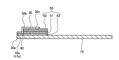
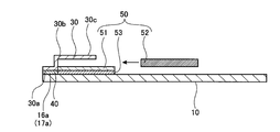
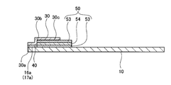
- FIG. 10 is a sectional view taken along line AA in FIG. 9. It is typical sectional drawing which shows the solar cell module concerning embodiment of this invention. It is typical sectional drawing which shows the connection of the back junction type solar cell and wiring tab concerning 2nd Embodiment of this invention. It is typical sectional drawing which shows the connection of the back junction type solar cell and wiring tab concerning 2nd Embodiment of this invention. It is typical sectional drawing which shows the connection of the back junction type solar cell and wiring tab concerning 3rd Embodiment of this invention.
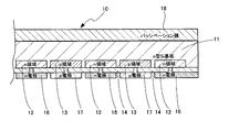
- FIG. 1 is a schematic cross-sectional view showing a solar cell according to an embodiment
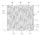
- FIG. 2 is a schematic plan view seen from the back side.
- the solar cell according to this embodiment is a back junction solar cell.
- the solar cell 10 has a p-type region 13 and an n-type region 12 on the back side of a substrate 11 made of a semiconductor wafer such as n-type single crystal silicon (Si).
- the p-type region 13 includes a plurality of finger portions extending in a line in one direction.
- the p-type region 13 includes a bus bar portion provided along one end portion of the substrate 11.
- the bus bar portion extends along a direction orthogonal to the one direction and is connected to a plurality of finger portions.
- the n-type region 12 includes a plurality of finger portions extending in a line in one direction.
- the n-type region 13 includes a bus bar portion provided along the other end portion of the substrate 11. The bus bar portion extends along a direction orthogonal to the one direction and is connected to a plurality of finger portions.
- the finger part of the p-type region 13 and the finger part of the n-type region 12 are arranged in parallel to each other with a predetermined interval.
- the p-type region 13 and the n-type region 12 are formed in the substrate 11 by the thermal diffusion method.
- the present invention is not limited to this, and a thin film forming method is formed on the back surface of the substrate 11. It may have a p-type semiconductor layer and an n-type semiconductor layer which are formed by using.
- Passivation films 18 and 14 are provided on the light receiving surface and the back surface of the substrate 11 in order to suppress surface recombination of carriers. These passivation films 18 and 14 are composed of a silicon oxide film or a silicon nitride film.
- the refractive index thereof is about 2.1. It can also be used as an antireflection film (AR layer) that suppresses reflection.
- a hole penetrating to the p region 13 or the n region 12 is provided at a predetermined position of the passivation film 14 formed on the back surface of the substrate 11.
- the shape of the hole is not particularly limited, and a shape such as a dot shape or a line shape is used.
- n-side electrode 16 is provided on the n-type region 12, and a p-side electrode 17 is provided on the p-type region 13.
- the n-side electrode 16 and the p-side electrode 17 are embedded in holes provided in the passivation film 14 and are electrically connected to the n-type region 12 and the p-type region 13, respectively.
- the n-side electrode 16 includes a bus bar portion 16-1 and a plurality of finger portions 16-2.
- the bus bar portion 16-1 and the plurality of finger portions 16-2 are provided corresponding to the bus bar portion and the plurality of finger portions of the n-type region 12.
- the p-side electrode 17 includes a bus bar portion 17-1 and a plurality of finger portions 17-2.
- the bus bar portion 17-1 and the plurality of finger portions 17-2 are provided corresponding to the bus bar portion and the plurality of finger portions of the p-type region 13.
- a conductive material such as copper, silver or aluminum is used so that a current generated in the solar cell can be taken out sufficiently. Further, copper or the like may be grown on an aluminum base electrode by plating to form a low resistance electrode.
- the bus bar portions 16-1 and 17-1 of the n-side electrode 16 and the p-side electrode 17 are provided with soldering areas 16a and 17a to which the wiring tabs are soldered in a row.
- soldering regions 16a and 17a are provided.
- the n-type single crystal silicon substrate 11 has a square shape of 125.5 mm square, and has a width amm near the center of the end of the n-type single crystal silicon substrate 11.
- a rectangular soldering area 16a (17a) having a length of bmm is provided.
- the width a is selected in the range of 5 mm to 9 mm
- the length b is selected in the range of 6 mm to 10 mm.
- a rectangular soldering region 16a (17a) having a width of 6 mm and a length of 7 mm is provided.
- a soldering area 16a (17a) of the same size is provided at intervals of 40 mm to 42 mm from the central soldering area to the left and right.
- the plurality of solar cells configured as described above are arranged linearly in one direction and are electrically connected to each other using a wiring material to constitute a solar cell string.
- the adjacent solar cells 10 and 10 are arranged so that the soldering region 16a of one solar cell 10 and the soldering region 17a of the other solar cell face each other.
- the solar cells 10 and 10 arranged adjacent to each other are electrically connected by a wiring member 33.
- the wiring member 33 is connected to the soldering regions 16a and 17a by solder.
- interval between the solar cells 10 and 10 is 2 mm.
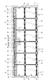
- the wiring tab 30 connected to the soldering area 16a (17a) is connected to the crossover wiring 31. And the electric current which flows through the crossover wiring 31 is taken out outside the solar cell module via the lead-out line 32a, 32b, 32c, 32d.
- the wiring tab 30, the transition wiring 31, and the lead lines 32 a, 32 b, 32 c, and 32 d are provided on the n-type electrode 16 and the p-type electrode 17.
- the insulating sheet 50 made of a filler or an insulating material is connected to the wiring tab 30, the transition wiring 31, and the lead wires 32a, 32b, 32c, 32d and the solar cell 10. It is sandwiched between.
- FIG. 6 is a plan view showing details of a connection portion between the soldering area and the wiring tab.
- the entire back surface of the solar cell 10 is covered so that the end of the n-type electrode 16 or the p-type electrode 17 is located up to a location of 1 mm or less, for example, 0.74 mm from the cell edge of the substrate 11.
- the n-type electrode 16 and the p-type electrode 17 are formed.
- the soldering region 16a (17a) is formed with a size of, for example, 6 mm ⁇ 7 mm.
- the area of the tab connecting portion 40a where the solder is provided is 3 mm ⁇ 3 mm, and is provided at a location 1.5 mm to 5.5 mm away from the cell edge, for example, 2.5 mm.
- the soldering region 16a (17a) is formed in a size more than twice the size of the tab connection portion 40a in consideration of an electrode formation error and a soldering alignment error.
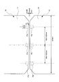
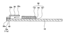
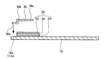
- the shape of the wiring tab 30 is formed in consideration of the thickness of the insulating sheet 50 made of a filler or an insulating material sandwiched between the wiring tab 30 and the substrate 11. That is, as shown in FIG. 6, the wiring tab 30 includes a flat portion 30a corresponding to the size of the tab connection portion 40a, a rising portion 30b rising from the flat portion 30a corresponding to the thickness of the insulating sheet 50, and a rising portion. An extending portion 30c that bends from 30b so as to be parallel to the flat portion 30a.
- the flat portion 30 a of the wiring tab 30 is bonded to the soldering region 16 a (17 a) of the solar cell 10 with solder 40.
- a space corresponding to the thickness of the insulating sheet 50 is formed between the extending portion 30c and the solar cell 10 by the rising portion 30b.
- the thickness of the wiring tab 30 is about 100 ⁇ m to 300 ⁇ m, and its width is smaller than the width of the soldering region 16a (17a) and wider than the width of the solder connection portion.
- the length is shorter than the sum of the width of the insulating sheet 50 and the width of the solder connection portion.
- the width of the insulating sheet 50 is 40 mm and the width of the solder connection portion is 3 mm, the width from the front end of the flat portion 30a to the rear end of the extending portion 30c is 40 mm.
- the flat portion 30a is formed to be longer than the 3 mm length of the tab connection portion 40a, including the alignment error.
- the height (x in the drawing) of the rising portion 30b is slightly larger than the thickness obtained by subtracting the thickness of the solder 40 from the thickness of the insulating sheet 50 so that the insulating sheet 50 is sandwiched between the raised portions 30b. Yes.
- the thickness of the solder 40 is 40 ⁇ m and the thickness of the insulating sheet 50 is 600 ⁇ m
- the height x is slightly wider than 560 ⁇ m.
- the thickness of the insulating sheet 50 may be set equal to the height of the insulating sheet 50 without reducing the thickness of the solder 40.
- an insulating sheet 50 made of a filler such as EVA (ethylene vinyl acetate), PVB (polyvinyl butyral), or olefin resin is interposed between the extending portion 30 c and the solar cell 10. Sandwich. Since a space corresponding to the thickness of the insulating sheet 50 is formed between the extending portion 30 c and the solar cell 10, the insulating sheet 50 can be inserted to the vicinity of the solder connection portion or a close contact portion. For this reason, insulation in the vicinity of the connecting portion between the solar cell 10 and the wiring tab 30 is ensured by the insulating sheet 50. As shown in FIG.
- an insulating sheet 50 is sandwiched between the wiring tab 30 and the crossover wiring 31 and the solar cell 10 in proximity to or in close contact with the solder 40.
- FIG. 10 showing a cross section taken along the line AA of FIG. 9, the insulating sheet 50 is in close contact with the connection portion by the solder 40, and the insulating sheet 50 is disposed on the n-type electrode 16 and the p-type electrode 17. Therefore, a short circuit due to the wiring tab 30 and the crossover wiring 31 is prevented.
- the solar cell module electrically connects the p-side electrode 17 of one solar cell 10 and the n-side electrode 16 of the other solar cell 10 using a wiring tab 30 and a crossover wiring 31. Further, as shown in FIG. 4, the transition wiring 31 is connected to output wirings 32a, 32b, 32c, and 32d for taking out the output to the outside of the module.
- the output wirings 32a, 32b, 32c, and 32d are connected to terminals of a terminal box (not shown).
- the output wirings 32a, 32b, 32c, and 32d are obtained by covering the entire surface of a copper foil having a thickness of about 100 ⁇ m to 300 ⁇ m and a width of about 6 mm with solder, and cutting them to a predetermined length and soldering them to the crossover wiring 31. Yes.
- the surfaces of the output wirings 32a, 32b, 32c, and 32d are covered with an insulating film.
- the solar cell module includes a surface protection member 20 made of a translucent material such as glass from the light receiving surface side, a translucent sealing material 22 such as EVA, a plurality of solar cells 10 constituting a solar cell string, and a back surface.
- the side sealing material 22 and the back surface protection member 21 are stacked in this order, laminated and integrated.
- the insulating sheet 50 made of the filler is cross-linked and integrated with the solar cell 10 and the wiring tab 30 being connected.
- the solar cell 10, the insulating sheet 50, the wiring tab 30, the transition wiring 31, and the like are brought into close contact with each other so that no bubbles are generated.
- the insulating sheet 50 such as a filler is integrated in the vicinity of or in close contact with the connection portion between the solar cell 10 and the wiring tab 30, so that the bus bar electrode 16-1 around the soldering region 16a (17a) ( Insulation with respect to the wiring tab 30 and the crossover wiring 31 can be ensured without increasing the area 17-1).
- the insulating sheet 50 made of a filler or the like can be installed in the vicinity of the connection portion between the wiring tab 30 and the solar cell 10 without applying a load to the solar cell 10. For this reason, the crack of the thick solar cell 10 etc. can be prevented, and a yield and reliability can be improved.
- the gap is provided between the solar cell 10 and the wiring tab 30 as much as the insulating sheet 50 is inserted, the insulating sheet 50 can be easily installed.
- insulating sheet 50 a single filler is used as the insulating sheet 50, but various types of insulating sheets 50 can be used.
- an insulating sheet provided with an adhesive layer such as an adhesive or an adhesive on one side is used as the insulating sheet 50
- the insulating sheet 50 shown in FIGS. 12 and 13 is made of an adhesive or an adhesive on one surface of an insulating substrate 51 such as PET (polyethylene terephthalate), PVF (polyvinyl fluoride), PEN (polyethylene naphthalate), PE (polyethylene).
- An adhesive layer 53 is provided.
- EVA, EEA ethylene ethyl acrylate
- PVB polyolefin resin
- an acrylic adhesive, a silicon adhesive, a rubber adhesive, or a urethane adhesive can be used as the adhesive.
- the insulating substrate 51 has a thickness of 50 ⁇ m to 75 ⁇ m, and the adhesive layer 53 has a thickness of 25 ⁇ m to 45 ⁇ m. It is necessary to sandwich an adhesive layer 52 such as a filler on the side where the adhesive layer 53 is not provided.
- the adhesive layer 53 is disposed so as to face the solar cell 10, and the insulating base material 51 is attached to the solar cell 10 by the adhesive layer 53.
- the contact bonding layer 52 which consists of a filler on the insulating base material 51 is inserted.
- the thickness of the adhesive layer 52 is about 600 ⁇ m.
- a space corresponding to the thickness of the insulating sheet 50 including the adhesive layer 53, the insulating base material 51, and the adhesive layer 52 is provided between the extending portion 30 c of the wiring tab 30 and the solar cell 10. Is formed.
- solder connection between the wiring tab 30 and the solar cell 10 may be performed after the insulating base material 51 is bonded to the solar cell 10 with the adhesive layer 53, in addition to the insulating sheet 50 being sandwiched.
- Adhesive layers 53 such as an adhesive material and an adhesive are provided on both surfaces of the insulating substrate 51.
- the insulating substrate 51 has a thickness of 50 ⁇ m to 75 ⁇ m, and the adhesive layer 53 has a thickness of 25 ⁇ m to 45 ⁇ m.
- one adhesive layer 53 is disposed facing the solar cell 10 side, and the insulating sheet 50 is attached to the solar cell 10 with the other adhesive layer 53.
- stretching part 30c is arrange
- a space corresponding to the thickness of the insulating sheet 50 including the adhesive layer 53, the insulating base 51, and the adhesive layer 53 is formed between the extending portion 30 c of the wiring tab 30 and the solar cell 10.
- the solder connection between the wiring tab 30 and the solar cell 10 is performed by first bonding the flat portion 30 a of the wiring tab 30 to the soldering region 16 a (17 a) of the solar cell 10 with the solder 40. To do. Thereafter, the insulating sheet 50 is sandwiched between the solar cell 10 and the wiring tab 30, and the solar cell 10 and the wiring tab 30 are bonded by the adhesive layer 53.
- the wiring tab 30 and the soldering region 16 a (17 a) of the solar cell 10 are soldered to the solar cell 10. You may connect.
- the insulating sheet 50 can be smoothly inserted into the space portion because it does not adhere to the solar cell 10 and the wiring tab 30 until the heat treatment at the time of lamination. Good workability.
- the insulating sheet 50 when the adhesive layer 53 is sticky at room temperature, the insulating sheet 50 is first attached to the predetermined position of the solar cell 10 by the adhesive layer 53.
- the wiring sheet 30 may be connected to the soldering region 16a (17a) of the solar cell 10 by the solder 40 with the insulating sheet positioned.
- the present invention is not limited to this, and the solar cell module using the solar cell having electrodes on both sides of the semiconductor wafer. It can also be applied to.
Landscapes
- Photovoltaic Devices (AREA)
Abstract
この発明は、太陽電池10の裏面上に配された配線材を有する太陽電池モジュールであって、太陽電池10の電極部の半田付け領域16a(17a)と接続される配線タブ30と、配線材タブ30と太陽電池10の間に挟み込まれる絶縁シート50と、を備え、配線タブ30は、半田付けされる領域に対応する平坦部30aと、平坦部30aから絶縁シート50の厚みに対応して立ち上がる立ち上がり部30bと、立ち上がり部30aから平坦部30aと平行になるように折れ曲がる延伸部30cと、からなる。 上記の構成とすることにより、太陽電池モジュール作製の際に、延伸部30cと太陽電子10の間には、絶縁シート50の厚みに相当する空隙が形成されているので、絶縁シート50を半田接続箇所の近傍または密接する箇所まで挿入でき、太陽電池モジュール作製における作業性が向上する。
Description
この発明は、太陽電池の裏側に配された配線を有する太陽電池モジュールに関するものである。
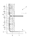
太陽電池モジュールは、電気的に接続された複数の太陽電池を有する複数の太陽電池ストリング、太陽電池ストリング同士の電気的な接続を行う渡り配線と、太陽電池の発電電力を外部に取出すための取出し配線とを有している。従来、太陽電池モジュールの発電効率を高めるために、配線材を折り曲げて太陽電池の裏側に配する構造が検討されている。かかる従来のモジュールでは、図17に示すように、半田400で取り付けた配線材300と太陽電池100との間の電気的接触を防止するために、配線材300と太陽電池100との間に、ポリエチレンテレフタレートからなる絶縁シート500を介在させている(例えば、特許文献1参照)。
しかしながら、上記の絶縁シートを太陽電池と配線材との間に挿入しようとすると、図17に示すように、作業性が悪い場合があった。
この発明は、上記の点に鑑み、作業性の向上した太陽電池モジュールを提供することを目的とする。
この発明は、太陽電池の裏面上に配された配線材を有する太陽電池モジュールであって、前記配線材と太陽電池の間に挟み込まれる絶縁シートを備え、前記配線材は、半田付けされる領域に対応する平坦部と、平坦部から絶縁シートの厚みに対応して立ち上がる立ち上がり部と、立ち上がり部から平坦部と平行になるように折れ曲がる延伸部と、からなる。
この発明によれば、配線材と太陽電池間の間に絶縁シートを容易に挟み込むことができ、作業性の向上した太陽電池モジュールを提供することができる。
実施形態について図面を参照しながら詳細に説明する。なお、図中同一または相当部分には同一符号を付し、説明の重複を避けるためにその説明は繰返さない。
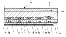
図1は、実施形態にかかる太陽電池を示す模式的断面図であり、図2は裏面側から見た模式的平面図である。この実施形態に係る太陽電池は、裏面接合型の太陽電池である。太陽電池10は、n型単結晶シリコン(Si)等の半導体ウエハからなる基板11の裏面側にp型領域13およびn型領域12を有している。
p型領域13は、一の方向にライン状に延びるフィンガー部を複数含んでいる。またp型領域13は、基板11の一端部に沿って設けられたバスバー部を含んでいる。バスバー部は前記一の方向と直交する方向に沿って延び、複数のフィンガー部と接続する。
n型領域12は、一の方向にライン状に延びるフィンガー部を複数含んでいる。またn型領域13は、基板11の他端部に沿って設けられたバスバー部を含んでいる。バスバー部は前記一の方向と直交する方向に沿って延び、複数のフィンガー部と接続する。
p型領域13のフィンガー部及びn型領域12のフィンガー部は、所定の間隔を隔てて互いに平行に配列されている。尚、図1は、p型領域13及びn型領域12を熱拡散法によって基板11内に作製したものであるが、本発明はこれに限るものではなく、基板11の裏面上に薄膜形成法を用いて形成されたp型半導体層及びn型半導体層を有するものであっても良い。
基板11の受光面上および裏面上には、キャリアの表面再結合を抑制するために、パッシベーション膜18、14が設けられている。これらのパッシベーション膜18、14は、シリコン酸化膜或いはシリコン窒化膜から構成される。
基板11の受光面上に形成されるパッシベーション膜18として、シリコン窒化膜を用いた場合には、その屈折率が2.1程度となるため、シリコン窒化膜は基板1の受光面における太陽光の反射を抑制する反射防止膜(AR層)としても用いることができる。
基板11の裏面上に形成されるパッシベーション膜14の所定箇所には、p領域13またはn領域12まで貫通する孔が設けられている。この孔の形状は特に限定されず、ドット状、ライン状等の形状が用いられる。
n型領域12上にはn側電極16、p型領域13上にはp側電極17が設けられている。n側電極16およびp側電極17は、パッシベーション膜14に設けられた孔の中を埋設し、n型領域12及びp型領域13に夫々電気的に接続する。n側電極16は、バスバー部16-1及び複数のフィンガー部16-2を含んでいる。バスバー部16-1及び複数のフィンガー部16-2は、n型領域12のバスバー部及び複数のフィンガー部に対応して設けられる。p側電極17は、バスバー部17-1及び複数のフィンガー部17-2を含んでいる。バスバー部17-1及び複数のフィンガー部17-2は、p型領域13のバスバー部及び複数のフィンガー部に対応して設けられる。
電極16、17の材料としては、太陽電池に発生する電流を外部に十分に取り出すことができるように、銅、銀又はアルミニウムなどの導電材料が用いられる。さらに、メッキにより銅などをアルミニウムの下地電極上に成長させ、低抵抗の電極を形成しても良い。
後述するように、n側電極16及びp側電極17のバスバー部16-1、17-1には、配線タブが半田付けされる半田付け領域16a、17aが電極と連なって設けられている。この実施形態では、半田付け領域16a、17aがそれぞれ3箇所ずつ設けられている。
この実施形態では、図3に示すように、n型単結晶シリコン基板11は、125.5mm角の正方形状のものが用いられ、n型単結晶シリコン基板11の端部の中央付近に幅amm、長さbmmの矩形状の半田付け領域16a(17a)が設けられる。幅aは、5mm~9mmの範囲で選択され、長さbは6mm~10mmの範囲で選択される。この実施形態では、例えば、幅6mm、長さ7mmの矩形状の半田付け領域16a(17a)が設けられる。そして、その中央の半田付け領域から左右にそれぞれ40mm~42mmの間隔を開けて、同様の大きさの半田付け領域16a(17a)が設けられている。
以上のように構成された複数の太陽電池は、一の方向に直線状に配列され、配線材を用いて互いに電気的に接続され、太陽電池ストリングを構成する。図3に示すように、隣り合う太陽電池10,10は、一方の太陽電池10の半田付け領域16aと他方の太陽電池の半田付け領域17aとが互いに対向するように配列される。図4に示すように、隣り合って配列された太陽電池10、10は、配線材33によって電気的に接続される。尚、配線材33は半田によって半田付け領域16a,17aに夫々接続される。また、太陽電池10、10間の間隔は2mmである。
また、図4、図5に示すように、半田付け領域16a(17a)に接続した配線タブ30が渡り配線31に接続される。そして、渡り配線31を流れる電流は、引き出し線32a、32b、32c、32dを介して、太陽電池モジュールの外部に取り出される。このように、配線タブ30、渡り配線31、引き出し線32a、32b、32c、32dがn型電極16、p型電極17の上に設けられる。このような場合には、配線による短絡を防止するために、充填材または絶縁材等からなる絶縁シート50が配線タブ30、渡り配線31及び引き出し線32a、32b、32c、32dと太陽電池10との間に挟み込まれる。
図6は、半田付け領域と配線タブの接続部の詳細を示す平面図である。図6に示すように、基板11のセル端部から1mm以下、例えば、0.74mmの箇所までn型電極16またはp型電極17の端が位置するように、太陽電池10の裏面全体を覆うように、n型電極16及びp型電極17が形成されている。前述したように、半田付け領域16a(17a)は、例えば6mm×7mmの大きさで形成される。半田が設けられるタブ接続箇所40aの面積は、3mm×3mmで、セル端から1.5mm~5.5mm、例えば、2、5mm離れた箇所に設けられる。ここで、半田付け領域16a(17a)は、電極形成誤差、半田付けの位置合わせ誤差を考慮して、タブ接続箇所40aの倍以上の大きさに形成されている。
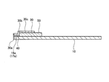
さて、この実施形態では、配線タブ30の形状が、配線タブ30と基板11との間に挟み込む充填材または絶縁材からなる絶縁シート50の厚みを考慮して形成されている。すなわち、図6に示すように、配線タブ30は、タブ接続箇所40aの大きさに対応する平坦部30aと、平坦部30aから絶縁シート50の厚みに対応して立ち上がる立ち上がり部30bと、立ち上がり部30bから平坦部30aと平行になるように折れ曲がる延伸部30cと、を有するように形成されている。
図7に示すように、太陽電池10の半田付け領域16a(17a)に、配線タブ30の平坦部30aを半田40にて接着する。太陽電池10に半田で取り付けられた配線タブ30は、立ち上がり部30bにより、延伸部30cと太陽電池10の間には、絶縁シート50の厚みに相当する空間が形成されている。
配線タブ30の厚さは100μm~300μm程度で、その幅は、半田付け領域16a(17a)の幅より狭く半田接続箇所の幅より広く形成されている。長さは、絶縁シート50の幅と半田接続箇所の幅の和より短く形成されている。この実施形態では、絶縁シート50の幅は40mm、半田接続箇所の幅は3mmであるので、平坦部30aの先端から延伸部30cの後端まで40mmとしている。
平坦部30aは、タブ接続箇所40aの長さ3mmより位置合わせの誤差を含めた分長く形成されている。立ち上がり部30bの高さ(図中x)は、半田付けをした後に、絶縁シート50が間に挟め込まれるように、絶縁シート50の厚みから半田40の厚みを引いた厚みより若干大きくしている。例えば、半田40の厚みが40μm、絶縁シート50の厚みが600μmの場合、この高さxは560μmより若干広くしている。なお、半田40の厚みを引かずに、絶縁シート50の厚み分の高さと同等に設定しても良い。
図7、図8に示すように、EVA(エチレンビニルアセテート)、PVB(ポリビニルブチラール)、オレフィン系樹脂等の充填材からなる厚み600μmの絶縁シート50を延伸部30cと太陽電池10との間に挟み込む。延伸部30cと太陽電池10の間には、絶縁シート50の厚みに相当する空間が形成されているので、絶縁シート50は、半田接続箇所の近傍または密接する箇所まで挿入できる。このため、太陽電池10と配線タブ30との間の接続部近傍の絶縁が絶縁シート50によって確保される。図9に示すように、配線タブ30並びに渡り配線31と太陽電池10との間には、半田40に近接または密接して絶縁シート50が挟み込まれている。図9のA-A線断面を示す図10に示すように、絶縁シート50が半田40による接続部に密接し、そして、n型電極16、p型電極17の上に絶縁シート50が配置されているので、配線タブ30、渡り配線31による短絡は防止されている。
太陽電池モジュールは、一方の太陽電池10のp側電極17と他方の太陽電池10のn側電極16とを配線タブ30、渡り配線31を用いて電気的に接続する。さらに、図4に示すように、渡り配線31は、モジュール外部に出力を取り出す出力配線32a、32b、32c、32dと接続されている。出力配線32a、32b、32c、32dは、端子ボックス(図示しない)の端子と接続される。通常、出力配線32a、32b、32c、32dは、厚さ100μm~300μm程度、幅6mm程度の銅箔の全面を半田で覆い、所定の長さに切断したものが渡り配線31に半田付けされている。また、出力配線32a、32b、32c、32dの表面は、絶縁フィルムによって被覆されている。
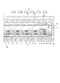
太陽電池モジュールは、受光面側からガラス等の透光性の材料からなる表面保護部材20、EVA等の透光性を有する封止材22、太陽電池ストリングを構成する複数の太陽電池10、裏面側の封止材22、裏面保護部材21をこの順序で積み重ね、ラミネートされて一体化される。このラミネート処理により、図11に示すように、充填材からなる絶縁シート50は架橋され、太陽電池10と配線タブ30とが接続された状態で一体化される。図11に示すように、太陽電池10、絶縁シート50、配線タブ30、渡り配線31等は、密着して一体化されるので、気泡等の発生は無い。
このように、太陽電池10と配線タブ30との接続部近傍または密接して充填材等の絶縁シート50が一体化されるため、半田付け領域16a(17a)の周囲のバスバー電極16-1(17-1)の領域を広くすることなく配線タブ30、渡り配線31に対する絶縁を確保できる。これによって、フィンガー電極16-2(17-2)を設ける領域を広くすることが可能となり、出力の向上に寄与する。また、配線タブ30と太陽電池10間の接続部近傍で、太陽電池10に負荷をかけることなく、充填材等からなる絶縁シート50を設置することができる。このため、太太陽電池10の割れなどが防げ、歩留まりや信頼性を向上させることができる。
また、太陽電池10と配線タブ30との間に、絶縁シート50が挿入される分だけの空隙が設けられているので、絶縁シート50の設置が容易に行える。
上記した実施形態においては、絶縁シート50として、単体の充填材を用いているが、絶縁シート50としては、種々のものを用いることができる。
第2の実施形態として、例えば、絶縁シート50として、片面に粘着材や接着剤等の接着層を設けた絶縁シートを用いた例を図12及び図13を参照して説明する。図12及び図13に示す絶縁シート50は、PET(ポリエチレンテレフタレート)、PVF(ポリビニルフロライド)、PEN(ポリエチレンナフタレート)、PE(ポリエチレン)などの絶縁基材51の片面に粘着材や接着剤等の接着層53が設けられている。粘着材用樹脂材料としては、EVA、EEA(エチレンエチルアクリレート)、PVB、オレフィン系樹脂を用いることができる。また、接着剤としては、アクリル系接着剤、シリコン系接着剤、ゴム系接着剤、ウレタン系接着剤を用いることができる。絶縁基材51の厚みは50μm~75μm、接着層53の厚みは25μm~45μmである。接着層53を設けていない側には、充填材等の接着層52を挟み込む必要がある。この第2の実施形態では、接着層53を太陽電池10側に面して配置し、接着層53によって太陽電池10に絶縁基材51を貼り付ける。そして、図13に示すように、絶縁基材51の上に充填材からなる接着層52を挿入している。この接着層52の厚みは、600μm程度である。
図12及び図13に示すように、配線タブ30の延伸部30cと太陽電池10の間には、接着層53、絶縁基材51、接着層52からなる絶縁シート50の厚みに相当する空間が形成されている。
また、配線タブ30と太陽電池10との間の半田接続は、絶縁シート50を挟み込む前に行う以外に、接着層53で太陽電池10に絶縁基材51を接着した後に行ってもよい。
第3の実施形態として、例えば、絶縁シート50として、両面に粘着材や接着剤等の接着層を設けた絶縁シートを用いた例を図14及び図15を参照して説明する。絶縁基材51の両面に粘着材や接着剤等の接着層53が設けられている。絶縁基材51の厚みは50μm~75μm、接着層53の厚みは25μm~45μmである。この第3の実施形態では、一方の接着層53を太陽電池10側に面して配置し、太陽電池10に他方の接着層53で絶縁シート50を貼り付ける。そして、図13に示すように、絶縁基材51の接着層53上に延伸部30cが配置される。
このため、配線タブ30の延伸部30cと太陽電池10の間には、接着層53、絶縁基材51、接着層53からなる絶縁シート50の厚みに相当する空間が形成されている。
図15に示すように、配線タブ30と太陽電池10との間の半田接続は、まず、太陽電池10の半田付け領域16a(17a)に、配線タブ30の平坦部30aを半田40にて接着する。その後、太陽電池10と配線タブ30との間に絶縁シート50を挟み込み、接着層53で太陽電池10、配線タブ30がそれぞれ接着される。
第3の実施形態について、図16に示すように、接着層53で太陽電池10に絶縁シート50を接着した後、配線タブ30と太陽電池10の半田付け領域16a(17a)に、半田40により接続してもよい。
また、接着層53として、EVA等の熱可逆性樹脂を用いると、ラミネート時の熱処理まで太陽電池10、配線タブ30と接着しないので、スムーズに空間部に絶縁シート50を挿入させることができ、作業性が良い。
また、第3の実施形態の変形例として、接着層53が常温で粘着性を有するものである場合には、先に太陽電池10の所定の位置に接着層53により絶縁シート50を貼り付けておき、その絶縁シートを位置決めとして、配線タブ30を太陽電池10の半田付け領域16a(17a)に半田40により接続しても良い。
例えば、上記の実施形態では裏面接合型の太陽電池を用いた太陽電池モジュールについて説明したが、本発明はこれに限るものではなく、半導体ウエハの両面に電極を備える太陽電池を用いた太陽電池モジュールにも適用することができる。
今回開示された実施の形態はすべての点で例示であって制限的なものではないと考えられるべきである。この発明の範囲は、上記した実施の形態の説明ではなくて特許請求の範囲によって示され、特許請求の範囲と均等の意味および範囲内でのすべての変更が含まれることが意図される。
10 太陽電池
11 基板
12 n型領域
13 p型領域
16 n型電極
17 p型電極
16a、17a 半田付け領域
30 配線タブ
30a 平坦部
30b 立ち上がり部
30c 延伸部
50 絶縁シート
11 基板
12 n型領域
13 p型領域
16 n型電極
17 p型電極
16a、17a 半田付け領域
30 配線タブ
30a 平坦部
30b 立ち上がり部
30c 延伸部
50 絶縁シート
Claims (6)
- 太陽電池の裏面上に配された配線材を有する太陽電池モジュールであって、
前記配線材と太陽電池の間に挟み込まれる絶縁シートを備え
前記配線材は、半田付けされる領域に対応する平坦部と、平坦部から絶縁シートの厚みに対応して立ち上がる立ち上がり部と、立ち上がり部から平坦部と平行になるように折れ曲がる延伸部と、を有する、太陽電池モジュール。 - 前記太陽電池に、前記配線材の平坦部より面積が大きく形成された半田付け領域が設けられている、請求項1に記載の太陽電池モジュール。
- 前記絶縁シートは充填材で形成されている、請求項1に記載の太陽電池モジュール。
- 前記絶縁シートは、絶縁基材の両面に接着層が設けられている請求項1に記載の太陽電池モジュール。
- 前記接着層は熱可逆性樹脂からなる請求項4に記載の太陽電池モジュール。
- 前記太陽電池は、裏面接合型の太陽電池である、請求項1乃至5のいずれか1項に記載の太陽電池モジュール。
Priority Applications (2)
| Application Number | Priority Date | Filing Date | Title |
|---|---|---|---|
| JP2012550809A JPWO2012090694A1 (ja) | 2010-12-28 | 2011-12-13 | 太陽電池モジュール |
| US13/929,068 US20130284232A1 (en) | 2010-12-28 | 2013-06-27 | Solar cell module |
Applications Claiming Priority (2)
| Application Number | Priority Date | Filing Date | Title |
|---|---|---|---|
| JP2010293027 | 2010-12-28 | ||
| JP2010-293027 | 2010-12-28 |
Related Child Applications (1)
| Application Number | Title | Priority Date | Filing Date |
|---|---|---|---|
| US13/929,068 Continuation US20130284232A1 (en) | 2010-12-28 | 2013-06-27 | Solar cell module |
Publications (1)
| Publication Number | Publication Date |
|---|---|
| WO2012090694A1 true WO2012090694A1 (ja) | 2012-07-05 |
Family
ID=46382810
Family Applications (1)
| Application Number | Title | Priority Date | Filing Date |
|---|---|---|---|
| PCT/JP2011/078751 Ceased WO2012090694A1 (ja) | 2010-12-28 | 2011-12-13 | 太陽電池モジュール |
Country Status (3)
| Country | Link |
|---|---|
| US (1) | US20130284232A1 (ja) |
| JP (1) | JPWO2012090694A1 (ja) |
| WO (1) | WO2012090694A1 (ja) |
Cited By (3)
| Publication number | Priority date | Publication date | Assignee | Title |
|---|---|---|---|---|
| JPWO2016068051A1 (ja) * | 2014-10-31 | 2017-08-31 | シャープ株式会社 | 光電変換素子、それを備えた太陽電池モジュールおよび太陽光発電システム |
| JP2019102616A (ja) * | 2017-11-30 | 2019-06-24 | 株式会社カネカ | 太陽電池モジュール及びその製造方法 |
| US12261229B1 (en) | 2023-11-07 | 2025-03-25 | Jinko Solar (Haining) Co., Ltd. | Solar cell and photovoltaic module |
Families Citing this family (3)
| Publication number | Priority date | Publication date | Assignee | Title |
|---|---|---|---|---|
| USD765024S1 (en) * | 2013-12-11 | 2016-08-30 | Solaero Technologies Corp. | Solar cell |
| USD765590S1 (en) * | 2013-12-11 | 2016-09-06 | Solaero Technologies Corp. | Solar cell |
| US10483410B2 (en) * | 2015-10-20 | 2019-11-19 | Alta Devices, Inc. | Forming front metal contact on solar cell with enhanced resistance to stress |
Citations (5)
| Publication number | Priority date | Publication date | Assignee | Title |
|---|---|---|---|---|
| JP2000332284A (ja) * | 1999-05-24 | 2000-11-30 | Kyocera Corp | 太陽電池モジュール |
| JP2003086820A (ja) * | 2001-06-29 | 2003-03-20 | Sharp Corp | 太陽電池モジュールおよびその製造方法 |
| JP2005340756A (ja) * | 2004-04-28 | 2005-12-08 | Sharp Corp | 太陽電池モジュール用一体型配線部材、それを用いた太陽電池モジュールおよびそれらの製造方法 |
| JP2006310745A (ja) * | 2005-03-29 | 2006-11-09 | Kyocera Corp | 太陽電池モジュール及びその製造方法 |
| JP2007165773A (ja) * | 2005-12-16 | 2007-06-28 | Sharp Corp | 太陽電池モジュールおよび出力リードフレーム |
Family Cites Families (2)
| Publication number | Priority date | Publication date | Assignee | Title |
|---|---|---|---|---|
| US9184327B2 (en) * | 2006-10-03 | 2015-11-10 | Sunpower Corporation | Formed photovoltaic module busbars |
| US20090139557A1 (en) * | 2007-11-30 | 2009-06-04 | Douglas Rose | Busbar connection configuration to accommodate for cell misalignment |
-
2011
- 2011-12-13 WO PCT/JP2011/078751 patent/WO2012090694A1/ja not_active Ceased
- 2011-12-13 JP JP2012550809A patent/JPWO2012090694A1/ja active Pending
-
2013
- 2013-06-27 US US13/929,068 patent/US20130284232A1/en not_active Abandoned
Patent Citations (5)
| Publication number | Priority date | Publication date | Assignee | Title |
|---|---|---|---|---|
| JP2000332284A (ja) * | 1999-05-24 | 2000-11-30 | Kyocera Corp | 太陽電池モジュール |
| JP2003086820A (ja) * | 2001-06-29 | 2003-03-20 | Sharp Corp | 太陽電池モジュールおよびその製造方法 |
| JP2005340756A (ja) * | 2004-04-28 | 2005-12-08 | Sharp Corp | 太陽電池モジュール用一体型配線部材、それを用いた太陽電池モジュールおよびそれらの製造方法 |
| JP2006310745A (ja) * | 2005-03-29 | 2006-11-09 | Kyocera Corp | 太陽電池モジュール及びその製造方法 |
| JP2007165773A (ja) * | 2005-12-16 | 2007-06-28 | Sharp Corp | 太陽電池モジュールおよび出力リードフレーム |
Cited By (5)
| Publication number | Priority date | Publication date | Assignee | Title |
|---|---|---|---|---|
| JPWO2016068051A1 (ja) * | 2014-10-31 | 2017-08-31 | シャープ株式会社 | 光電変換素子、それを備えた太陽電池モジュールおよび太陽光発電システム |
| US11316061B2 (en) | 2014-10-31 | 2022-04-26 | Sharp Kabushiki Kaisha | Photovoltaic devices, photovoltaic modules provided therewith, and solar power generation systems |
| JP2019102616A (ja) * | 2017-11-30 | 2019-06-24 | 株式会社カネカ | 太陽電池モジュール及びその製造方法 |
| US12261229B1 (en) | 2023-11-07 | 2025-03-25 | Jinko Solar (Haining) Co., Ltd. | Solar cell and photovoltaic module |
| JP2025077932A (ja) * | 2023-11-07 | 2025-05-19 | 晶科能源(海▲寧▼)有限公司 | 太陽電池及びその製造方法、光起電力モジュール |
Also Published As
| Publication number | Publication date |
|---|---|
| JPWO2012090694A1 (ja) | 2014-06-05 |
| US20130284232A1 (en) | 2013-10-31 |
Similar Documents
| Publication | Publication Date | Title |
|---|---|---|
| CN102047441B (zh) | 太阳能电池模块 | |
| US20120048335A1 (en) | Wiring sheet, wiring sheet-equipped solar cells, and solar cell module | |
| CN203277411U (zh) | 太阳能电池模块 | |
| US11955569B2 (en) | Photovoltaic module | |
| CN102227821A (zh) | 太阳能电池模块及其制造方法 | |
| WO2018090445A1 (zh) | 一种带有旁路二极管的光伏叠片组件 | |
| WO2009148078A1 (ja) | 端子ボックス及び太陽電池モジュール | |
| JP2010056251A (ja) | 太陽電池モジュール | |
| JPWO2012090694A1 (ja) | 太陽電池モジュール | |
| CN106605304A (zh) | 太阳能电池组件和太阳能电池组件的制造方法 | |
| WO2014208312A1 (ja) | 太陽電池モジュール及びその製造方法 | |
| CN102687279B (zh) | 太阳能电池单元 | |
| CN118591892A (zh) | 太阳能电池及太阳能电池的制造方法 | |
| WO2013031296A1 (ja) | 太陽電池モジュール | |
| JP5306490B2 (ja) | 端子ボックス及び太陽電池モジュール | |
| JP5132646B2 (ja) | 端子ボックス及び太陽電池モジュール | |
| JP4883891B2 (ja) | 太陽電池モジュール | |
| JP2015029069A (ja) | 太陽電池モジュール | |
| WO2012090622A1 (ja) | 太陽電池モジュール | |
| JP5816823B2 (ja) | 太陽電池モジュール及びその製造方法 | |
| JP2015192065A (ja) | 太陽電池モジュール | |
| CN107155376B (zh) | 太阳能电池面板 | |
| JP7591922B2 (ja) | 太陽電池モジュール | |
| KR102728920B1 (ko) | 절연 인터커넥터를 갖춘 태양광 장치 | |
| JP2020107766A (ja) | 第1太陽電池モジュールおよび太陽電池システム |
Legal Events
| Date | Code | Title | Description |
|---|---|---|---|
| 121 | Ep: the epo has been informed by wipo that ep was designated in this application |
Ref document number: 11853995 Country of ref document: EP Kind code of ref document: A1 |
|
| ENP | Entry into the national phase |
Ref document number: 2012550809 Country of ref document: JP Kind code of ref document: A |
|
| NENP | Non-entry into the national phase |
Ref country code: DE |
|
| 122 | Ep: pct application non-entry in european phase |
Ref document number: 11853995 Country of ref document: EP Kind code of ref document: A1 |