WO2012086535A1 - 成膜材料の回収方法 - Google Patents
成膜材料の回収方法 Download PDFInfo
- Publication number
- WO2012086535A1 WO2012086535A1 PCT/JP2011/079151 JP2011079151W WO2012086535A1 WO 2012086535 A1 WO2012086535 A1 WO 2012086535A1 JP 2011079151 W JP2011079151 W JP 2011079151W WO 2012086535 A1 WO2012086535 A1 WO 2012086535A1
- Authority
- WO
- WIPO (PCT)
- Prior art keywords
- film forming
- forming material
- film
- magnet
- vapor deposition
- Prior art date
- Legal status (The legal status is an assumption and is not a legal conclusion. Google has not performed a legal analysis and makes no representation as to the accuracy of the status listed.)
- Ceased
Links
Images






Classifications
-
- B—PERFORMING OPERATIONS; TRANSPORTING
- B03—SEPARATION OF SOLID MATERIALS USING LIQUIDS OR USING PNEUMATIC TABLES OR JIGS; MAGNETIC OR ELECTROSTATIC SEPARATION OF SOLID MATERIALS FROM SOLID MATERIALS OR FLUIDS; SEPARATION BY HIGH-VOLTAGE ELECTRIC FIELDS
- B03C—MAGNETIC OR ELECTROSTATIC SEPARATION OF SOLID MATERIALS FROM SOLID MATERIALS OR FLUIDS; SEPARATION BY HIGH-VOLTAGE ELECTRIC FIELDS
- B03C1/00—Magnetic separation
- B03C1/005—Pretreatment specially adapted for magnetic separation
-
- B—PERFORMING OPERATIONS; TRANSPORTING
- B03—SEPARATION OF SOLID MATERIALS USING LIQUIDS OR USING PNEUMATIC TABLES OR JIGS; MAGNETIC OR ELECTROSTATIC SEPARATION OF SOLID MATERIALS FROM SOLID MATERIALS OR FLUIDS; SEPARATION BY HIGH-VOLTAGE ELECTRIC FIELDS
- B03C—MAGNETIC OR ELECTROSTATIC SEPARATION OF SOLID MATERIALS FROM SOLID MATERIALS OR FLUIDS; SEPARATION BY HIGH-VOLTAGE ELECTRIC FIELDS
- B03C1/00—Magnetic separation
- B03C1/02—Magnetic separation acting directly on the substance being separated
- B03C1/30—Combinations with other devices, not otherwise provided for
-
- C—CHEMISTRY; METALLURGY
- C23—COATING METALLIC MATERIAL; COATING MATERIAL WITH METALLIC MATERIAL; CHEMICAL SURFACE TREATMENT; DIFFUSION TREATMENT OF METALLIC MATERIAL; COATING BY VACUUM EVAPORATION, BY SPUTTERING, BY ION IMPLANTATION OR BY CHEMICAL VAPOUR DEPOSITION, IN GENERAL; INHIBITING CORROSION OF METALLIC MATERIAL OR INCRUSTATION IN GENERAL
- C23C—COATING METALLIC MATERIAL; COATING MATERIAL WITH METALLIC MATERIAL; SURFACE TREATMENT OF METALLIC MATERIAL BY DIFFUSION INTO THE SURFACE, BY CHEMICAL CONVERSION OR SUBSTITUTION; COATING BY VACUUM EVAPORATION, BY SPUTTERING, BY ION IMPLANTATION OR BY CHEMICAL VAPOUR DEPOSITION, IN GENERAL
- C23C14/00—Coating by vacuum evaporation, by sputtering or by ion implantation of the coating forming material
- C23C14/06—Coating by vacuum evaporation, by sputtering or by ion implantation of the coating forming material characterised by the coating material
- C23C14/12—Organic material
-
- C—CHEMISTRY; METALLURGY
- C23—COATING METALLIC MATERIAL; COATING MATERIAL WITH METALLIC MATERIAL; CHEMICAL SURFACE TREATMENT; DIFFUSION TREATMENT OF METALLIC MATERIAL; COATING BY VACUUM EVAPORATION, BY SPUTTERING, BY ION IMPLANTATION OR BY CHEMICAL VAPOUR DEPOSITION, IN GENERAL; INHIBITING CORROSION OF METALLIC MATERIAL OR INCRUSTATION IN GENERAL
- C23C—COATING METALLIC MATERIAL; COATING MATERIAL WITH METALLIC MATERIAL; SURFACE TREATMENT OF METALLIC MATERIAL BY DIFFUSION INTO THE SURFACE, BY CHEMICAL CONVERSION OR SUBSTITUTION; COATING BY VACUUM EVAPORATION, BY SPUTTERING, BY ION IMPLANTATION OR BY CHEMICAL VAPOUR DEPOSITION, IN GENERAL
- C23C14/00—Coating by vacuum evaporation, by sputtering or by ion implantation of the coating forming material
- C23C14/22—Coating by vacuum evaporation, by sputtering or by ion implantation of the coating forming material characterised by the process of coating
- C23C14/56—Apparatus specially adapted for continuous coating; Arrangements for maintaining the vacuum, e.g. vacuum locks
- C23C14/564—Means for minimising impurities in the coating chamber such as dust, moisture, residual gases
-
- H—ELECTRICITY
- H10—SEMICONDUCTOR DEVICES; ELECTRIC SOLID-STATE DEVICES NOT OTHERWISE PROVIDED FOR
- H10K—ORGANIC ELECTRIC SOLID-STATE DEVICES
- H10K71/00—Manufacture or treatment specially adapted for the organic devices covered by this subclass
- H10K71/20—Changing the shape of the active layer in the devices, e.g. patterning
- H10K71/221—Changing the shape of the active layer in the devices, e.g. patterning by lift-off techniques
-
- B—PERFORMING OPERATIONS; TRANSPORTING
- B03—SEPARATION OF SOLID MATERIALS USING LIQUIDS OR USING PNEUMATIC TABLES OR JIGS; MAGNETIC OR ELECTROSTATIC SEPARATION OF SOLID MATERIALS FROM SOLID MATERIALS OR FLUIDS; SEPARATION BY HIGH-VOLTAGE ELECTRIC FIELDS
- B03C—MAGNETIC OR ELECTROSTATIC SEPARATION OF SOLID MATERIALS FROM SOLID MATERIALS OR FLUIDS; SEPARATION BY HIGH-VOLTAGE ELECTRIC FIELDS
- B03C2201/00—Details of magnetic or electrostatic separation
- B03C2201/20—Magnetic separation of bulk or dry particles in mixtures
Definitions
- the present invention relates to a method for collecting a film forming material in which a film forming material attached to the surface of a film forming jig provided in a film forming chamber in a vacuum film forming apparatus is peeled off and recovered.
- the core component of the electronic device include a semiconductor, a flat display panel including a liquid crystal panel, a solar cell, a semiconductor device, and a memory.
- Such an electronic device is manufactured using a vacuum film forming apparatus using a vacuum film forming method such as a sputtering method, a vacuum vapor deposition method, or an ion plating method, and a rare metal is often used as a film forming material.
- a vacuum film forming method such as a sputtering method, a vacuum vapor deposition method, or an ion plating method
- a rare metal is often used as a film forming material.
- flat panel displays have been used in various products and fields, and further flat panel displays are required to have larger sizes, higher image quality, and lower power consumption.
- an organic EL display device including an organic EL element using electroluminescence (electroluminescence; hereinafter referred to as “EL”) of an organic material is an all-solid-state type, driven at a low voltage and has a high-speed response.
- EL electroluminescence
- the organic EL display device has, for example, a configuration in which an organic EL element connected to a TFT is provided on a substrate made of a glass substrate or the like provided with a TFT (thin film transistor).
- the organic EL element is a light emitting element that can emit light with high luminance by low-voltage direct current drive, and has a structure in which a first electrode, an organic EL layer, and a second electrode are stacked in this order. Of these, the first electrode is connected to the TFT.
- the organic EL layer a hole injection layer, a hole transport layer, an electron blocking layer, a light emitting layer, a hole blocking layer, an electron transport layer, an electron injection layer
- a hole injection layer a hole injection layer, a hole transport layer, an electron blocking layer, a light emitting layer, a hole blocking layer, an electron transport layer, an electron injection layer
- a full-color organic EL display device is generally formed by arranging organic EL elements of red (R), green (G), and blue (B) as sub-pixels on a substrate, and using TFTs. Image display is performed by selectively emitting light from these organic EL elements with a desired luminance.
- the organic EL element in the light emitting portion of such an organic EL display device is generally formed by stacking organic films.
- a light emitting layer made of an organic light emitting material that emits light of each color is formed in a predetermined pattern for each organic EL element that is a light emitting element.
- a vacuum evaporation method using an evaporation mask called a “shadow mask”, an ink jet method, a laser transfer method, or the like can be applied to film formation of a predetermined pattern by stacked evaporation.
- the vacuum deposition method uses a deposition source called a “crucible” or “boat” that contains a deposition material inside, and heats the deposition material under high vacuum to sublimate the substrate to be deposited.
- the said vapor deposition material is vapor-deposited on it.
- the vapor deposition material injected from the vapor deposition source as vapor deposition particles is vapor-deposited through an opening provided in the vapor deposition mask in a vacuum chamber of a vacuum vapor deposition apparatus, thereby obtaining a desired film formation pattern. be able to.
- the organic EL element in the light emitting part of the organic EL display device is formed by stacking organic films.
- the scattered vapor deposition particles also adhere to components other than the deposition target substrate such as a TFT substrate. .
- the vacuum chamber of the vacuum deposition apparatus there are various components such as a deposition plate and a shutter.
- the organic material constituting the organic film is expensive, the vapor deposition material adhering to these components, that is, the vapor deposition particles adhering to the film formation substrate such as a TFT substrate is wasted unless it is collected.
- material utilization efficiency shows the ratio of the material actually utilized among the materials used at the time of vapor deposition.
- Patent Document 1 discloses a method of heating and re-evaporating the vapor deposition material attached to the cell shutter and cooling and recovering the vapor with a shroud in which a cooling medium is circulated.
- Patent Document 2 discloses a method in which a vapor deposition material adhering to a shutter plate is heated and melted by a heater in the shutter, dropped into a vapor deposition source, and recovered.
- Patent Document 3 discloses a method of heating a cell shutter with a heater to evaporate vapor deposition material adhering to the lower surface of the cell shutter and recovering it in a crucible.
- a vapor deposition material recovery tool having a blocking wall and a vapor flow discharge port is arranged so as to cover the vapor outlet, and the divergence angle of the vapor flow from the vapor deposition source to the substrate to be processed is controlled. After vapor deposition, a method is disclosed in which the vapor deposition material recovery tool is taken out and the vapor deposition material deposited on the barrier wall is recovered.
- Patent Document 5 discloses that components such as a shutter in a chamber in which an organic material is deposited are made inactive materials that do not change the organic material, and the organic material deposited on these components is recovered.
- Patent Document 6 discloses a method of collecting deposits on a film forming jig by spraying a water jet.
- Patent Documents 1 to 3 have a problem that the vapor deposition material attached to portions other than the shutter cannot be recovered.
- the heating of the vapor deposition material may cause a deterioration of the vapor deposition material due to the heating.
- Patent Document 4 has a problem that the material attached to other than the blocking wall and the substrate to be processed cannot be recovered.
- Patent Document 5 discloses that an organic material deposited on a part such as a shutter in the chamber is recovered, but a specific recovery method is not disclosed.
- Patent Document 6 cannot be applied to a vapor deposition material that is easily denatured by moisture. Moreover, even with water, the film forming jig is damaged or peeled off by water pressure, and the peeled film forming jig is mixed into the peeled vapor deposition material. However, no mention is made of impurities mixed in this way.
- the conventional method could not collect the film forming material efficiently and at low cost.
- the present invention has been made in view of the above problems, and an object of the present invention is to provide a method for recovering a film forming material efficiently and at low cost.
- a method for collecting a film forming material peels off a film forming material attached to the surface of a film forming jig provided in a film forming chamber in a vacuum film forming apparatus.
- the method for collecting a film forming material peels off the film forming material attached to the surface of a film forming jig provided in a film forming chamber in a vacuum film forming apparatus.
- the debris of the cutting tool made of the material adsorbed by the magnet which is mixed with the delamination process that is scraped off and the film-depositing material delaminated in the delamination process, is adsorbed to the magnet and separated from the film-deposition material. And a separation step of collecting the film forming material.
- the surface of the film formation jig or tool is peeled off together with the film formation material, and mixed into the peeled film formation material. To do.
- a film forming jig provided with a layer made of a material adsorbed by a magnet at least in a part in contact with the film forming jig, or at least a part in contact with the film forming material,
- a cutting tool made of a material that is attracted to the magnet By using a cutting tool made of a material that is attracted to the magnet, the debris made of the material that is attracted to the magnet, which is peeled together with the film-forming material when the film-forming material is peeled off, is attracted to the magnet and formed. Separated from membrane material.
- the film forming material can be collected efficiently and at low cost.
- the film forming material can be recovered and reused with high purity without adding a complicated separation processing step.
- the debris adsorbed on the magnet can be separated and collected in the separation step. Therefore, cost recovery and environmental destruction prevention can be achieved by collecting the fragments.
- a film forming jig provided with a layer made of a material adsorbed by a magnet at least in a portion in contact with the film forming jig, or at least in contact with the film forming material.
- a cutting tool made of a material that is adsorbed to the magnet the piece made of the material adsorbed to the magnet that was peeled off together with the film forming material when the film forming material was peeled off is adsorbed to the magnet.
- (A)-(d) is a figure which shows the separation / recovery process of the film-forming material concerning Embodiment 1 of this invention in order of a process. It is sectional drawing which shows schematic structure of the vacuum evaporation system used in Embodiment 1 of this invention.
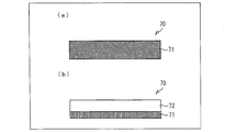
- (A) * (b) is sectional drawing which shows the layer structure of the component in a chamber in the vacuum evaporation system used in Embodiment 1 of this invention. It is sectional drawing which shows schematic structure of the principal part in the vacuum chamber after a vapor deposition process. It is sectional drawing which shows schematic structure of an organic electroluminescence display. It is sectional drawing which shows schematic structure of the organic EL element which comprises the display part of an organic EL display apparatus.
- the evaporation material used for forming the film forming pattern using the vacuum vapor deposition method in the manufacture of the organic EL display device is recovered.
- the case where it is performed will be described as an example.
- FIG. 5 is a cross-sectional view illustrating a schematic configuration of the organic EL display device.
- the organic EL display device 100 includes a TFT (thin film transistor) substrate 110, an organic EL element 120, an adhesive layer 130, and a sealing substrate 140.
- TFT thin film transistor
- a TFT or the like is formed as a switching element in a portion that becomes a pixel region.
- the organic EL element 120 is formed in a matrix in the display area of the TFT substrate 110.
- the TFT substrate 110 on which the organic EL element 120 is formed is bonded to the sealing substrate 140 with an adhesive layer 130 or the like.
- FIG. 6 is a cross-sectional view showing a schematic configuration of the organic EL element 120 constituting the display unit of the organic EL display device 100.
- the TFT substrate 110 has a configuration in which a TFT 112 (switching element) and wiring 113, an interlayer insulating film 114, an edge cover 115, and the like are formed on a transparent insulating substrate 111 such as a glass substrate. ing.
- the organic EL display device 100 is a full-color active matrix organic EL display device.
- red (R), green (G), blue On the insulating substrate 111, red (R), green (G), blue ( The pixels 101R, 101G, and 101B of the respective colors including the organic EL elements 120 of the respective colors B) are arranged in a matrix.
- the TFTs 112 are provided corresponding to the pixels 101R, 101G, and 101B, respectively.
- the structure of the TFT is conventionally well known. Therefore, illustration and description of each layer in the TFT 112 are omitted.
- the interlayer insulating film 114 is laminated over the entire area of the insulating substrate 111 on the insulating substrate 111 so as to cover each TFT 112 and the wiring 113.
- the first electrode 121 in the organic EL element 120 is formed on the interlayer insulating film 114.
- the interlayer insulating film 114 is provided with a contact hole 114a for electrically connecting the first electrode 121 in the organic EL element 120 to the TFT 112. Thereby, the TFT 112 is electrically connected to the organic EL element 120 through the contact hole 114a.
- the edge cover 115 prevents the first electrode 121 and the second electrode 126 in the organic EL element 120 from being short-circuited when the organic EL layer becomes thin or the electric field concentration occurs at the end of the first electrode 121.
- This is an insulating layer.
- the edge cover 115 is formed on the interlayer insulating film 114 so as to cover the end portion of the first electrode 121.
- the first electrode 121 is exposed at a portion where the edge cover 115 is not provided. This exposed portion becomes a light emitting portion of each of the pixels 101R, 101G, and 101B.
- each of the pixels 101R, 101G, and 101B is partitioned by the edge cover 115 having an insulating property.
- the edge cover 115 also functions as an element isolation film.
- insulating substrate 111 for example, alkali-free glass, plastic, or the like can be used. In the present embodiment, alkali-free glass having a thickness of 0.7 mm is used.
- the interlayer insulating film 114 and the edge cover 115 a known photosensitive resin can be used.
- the photosensitive resin include acrylic resin and polyimide resin.
- the TFT 112 is manufactured by a known method.
- the active matrix organic EL display device 100 in which the TFT 112 is formed in each of the pixels 101R, 101G, and 101B is taken as an example.
- the present embodiment is not limited to this, and the present invention can also be applied to the manufacture of a passive matrix organic EL display device in which TFTs are not formed.
- the organic EL element 120 is a light emitting element that can emit light with high luminance by low voltage direct current drive, and a first electrode 121, an organic EL layer, and a second electrode 126 are laminated in this order.
- the first electrode 121 is a layer having a function of injecting (supplying) holes into the organic EL layer. As described above, the first electrode 121 is connected to the TFT 112 through the contact hole 114a.
- a hole injection layer / hole transport layer 122 for example, from the first electrode 121 side, for example, a hole injection layer / hole transport layer 122, a light emitting layer 123R. 123G * 123B, the electron carrying layer 124, and the electron injection layer 125 have the structure formed in this order.
- a carrier blocking layer for blocking the flow of carriers such as holes and electrons may be inserted as necessary.
- One layer may have a plurality of functions. For example, one layer serving as both a hole injection layer and a hole transport layer may be formed.
- the stacking order is that in which the first electrode 121 is an anode and the second electrode 126 is a cathode.
- the order of stacking the organic EL layers is reversed.
- the hole injection layer is a layer having a function of increasing the hole injection efficiency into the light emitting layers 123R, 123G, and 123B.
- the hole transport layer is a layer having a function of improving the efficiency of transporting holes to the light emitting layers 123R, 123G, and 123B.
- the hole injection / hole transport layer 122 is uniformly formed on the entire display region of the TFT substrate 110 so as to cover the first electrode 121 and the edge cover 115.
- the hole injection layer / hole transport layer 122 in which the hole injection layer and the hole transport layer are integrated is provided as the hole injection layer and the hole transport layer. ing.
- this embodiment is not limited to this, and the hole injection layer and the hole transport layer may be formed as independent layers.
- light emitting layers 123R, 123G, and 123B are formed corresponding to the pixels 101R, 101G, and 101B, respectively.
- the light emitting layers 123R, 123G, and 123B are layers having a function of emitting light by recombining holes injected from the first electrode 121 side and electrons injected from the second electrode 126 side.
- the light emitting layers 123R, 123G, and 123B are each formed of a material having high light emission efficiency, such as a low molecular fluorescent dye or a metal complex.
- the electron transport layer 124 is a layer having a function of increasing the electron transport efficiency from the second electrode 126 to the light emitting layers 123R, 123G, and 123B.
- the electron injection layer 125 is a layer having a function of increasing the electron injection efficiency from the second electrode 126 to the light emitting layers 123R, 123G, and 123B.
- the electron transport layer 124 is formed on the light emitting layer 123R / 123G / 123B and the hole injection layer / hole transport layer 122 so as to cover the light emitting layer 123R / 123G / 123B and the hole injection layer / hole transport layer 122.
- the TFT substrate 110 is uniformly formed over the entire display area.
- the electron injection layer 125 is uniformly formed on the entire surface of the display region of the TFT substrate 110 on the electron transport layer 124 so as to cover the electron transport layer 124.
- the electron transport layer 124 and the electron injection layer 125 may be formed as independent layers as described above, or may be provided integrally with each other. That is, the organic EL display device 100 may include an electron transport layer / electron injection layer instead of the electron transport layer 124 and the electron injection layer 125.
- the second electrode 126 is a layer having a function of injecting electrons into the organic EL layer composed of the organic layers as described above.
- the second electrode 126 is uniformly formed on the electron injection layer 125 over the entire display region of the TFT substrate 110 so as to cover the electron injection layer 125.
- organic layers other than the light-emitting layers 123R, 123G, and 123B are not essential layers as the organic EL layer, and may be appropriately formed according to the required characteristics of the organic EL element 120.
- one layer may have a plurality of functions.
- a carrier blocking layer can be added to the organic EL layer as necessary. For example, by adding a hole blocking layer as a carrier blocking layer between the light emitting layers 123R, 123G, and 123B and the electron transport layer 124, holes are prevented from passing through the electron transport layer 124, thereby improving luminous efficiency. can do.
- the first electrode 121 is formed in a pattern corresponding to each of the pixels 101R, 101G, and 101B by photolithography and etching after an electrode material is formed by sputtering or the like.
- the first electrode 121 in the case of a bottom emission type organic EL element that emits light to the insulating substrate 111 side, it is necessary to be transparent or translucent.
- the second electrode 126 needs to be transparent or translucent.
- Examples of conductive film materials used for the first electrode 121 and the second electrode 126 include ITO (Indium Tin Oxide), IZO (Indium Zinc Oxide), gallium-doped zinc oxide (A transparent conductive material such as GZO) or a metal material such as gold (Au), nickel (Ni), or platinum (Pt) can be used.
- ITO Indium Tin Oxide
- IZO Indium Zinc Oxide
- GZO gallium-doped zinc oxide
- a transparent conductive material such as GZO
- a metal material such as gold (Au), nickel (Ni), or platinum (Pt) can be used.
- a sputtering method a vacuum deposition method, a CVD (chemical vapor deposition) method, a plasma CVD method, a printing method, or the like can be used.
- a sputtering method a vacuum deposition method
- a CVD (chemical vapor deposition) method a plasma CVD method, a printing method, or the like.
- stacking of the said 1st electrode 121 As shown in FIG.
- Each of the light emitting layers 123R, 123G, and 123B may be made of a single material, or may be a mixed material in which a certain material is used as a host material and another material is mixed as a guest material or a dopant. .
- Examples of the material of the hole injection layer, the hole transport layer, or the hole injection layer / hole transport layer 122 include anthracene, azatriphenylene, fluorenone, hydrazone, stilbene, triphenylene, benzine, styrylamine, triphenylamine, and porphyrin. , Triazoles, imidazoles, oxadiazoles, oxazoles, polyarylalkanes, phenylenediamines, arylamines, and derivatives thereof, thiophene compounds, polysilane compounds, vinylcarbazole compounds, aniline compounds, etc. A monomer, an oligomer, a polymer, etc. are mentioned.
- a material having high luminous efficiency such as a low molecular fluorescent dye or a metal complex is used.
- a material having high luminous efficiency such as a low molecular fluorescent dye or a metal complex.
- Examples of the material for the electron transport layer 124, the electron injection layer 125, or the electron transport layer / electron injection layer include tris (8-quinolinolato) aluminum complex, oxadiazole derivative, triazole derivative, phenylquinoxaline derivative, silole derivative, and the like. Can be mentioned.
- FIG. 2 is a cross-sectional view showing a schematic configuration of a vacuum vapor deposition apparatus used in the present embodiment.
- a vapor deposition apparatus 1 (vacuum vapor deposition apparatus, vacuum film formation apparatus) used in the present embodiment includes a vacuum chamber 10 as a film formation chamber.
- various components such as a vapor deposition source 20, a deposition plate 30, and a shutter 40 are provided.
- the vacuum chamber 10 has a vacuum pump (not shown) that evacuates the vacuum chamber 10 through an exhaust port (not shown) provided in the vacuum chamber 10 in order to keep the vacuum chamber 10 in a vacuum state during vapor deposition. Etc. are provided.
- the vacuum chamber 10 can be depressurized by a vacuum pump (not shown) or the like, and has an opening / closing portion, and is capable of attaching, removing, taking in and out various components provided in the vacuum chamber 10 so as to be detachable. Is possible.
- the vapor deposition source 20 injects a vapor deposition material such as an organic light emitting material as vapor deposition particles by heating and sublimating the vapor deposition material, which is a film forming material, under high vacuum.
- a vapor deposition material such as an organic light emitting material as vapor deposition particles by heating and sublimating the vapor deposition material, which is a film forming material, under high vacuum.
- the vapor deposition source 20 may be one in which a vapor deposition material is directly accommodated in a container disposed in a vacuum chamber and heated, and has a load-lock type pipe, and the sublimated vapor deposition material is loaded. You may inject through a lock-type piping.
- vapor deposition source 20 for example, a container called “crucible” or “boat” that contains a vapor deposition material therein is used.
- a vapor deposition mask 50 called a shadow mask in which an opening 51 (through hole, see FIG. 7) is formed at a desired position and shape is used.
- the vapor deposition source 20 is disposed opposite to the mask 50 disposed in the vacuum chamber 10 with a certain gap (that is, separated by a certain distance). Further, the vapor deposition source 20 is disposed so as to face the film formation surface 61 of the film formation substrate 60 through the mask 50 disposed in the vacuum chamber 10.
- the vapor deposition source 20 has an injection port 21 on the surface facing the mask 50 for injecting (scattering) the vapor deposition material as vapor deposition particles. Moreover, the vapor deposition source 20 shown in FIG. 2 has, for example, a mechanism for injecting vapor deposition particles upward.
- the vapor deposition source 20 is disposed below the deposition target substrate 60, and the deposition target substrate 60 is held in close contact with the mask 50 with the deposition target surface 61 facing downward. This is illustrated with an example of the case.
- a deposition plate 30 is disposed in a scattering region of the deposition particles that are not desired to be deposited (an extra scattering region other than the injection path, which is a necessary scattering region of the deposition particles). Is provided.
- a first deposition plate 31 and a second deposition plate 32 are provided as the deposition plate 30.
- the vapor deposition particle injection path connecting the injection port 21 of the vapor deposition source 20 and the opening region (opening group forming region) in the mask 50, which becomes a vapor flow discharge port, is excluded.
- a first deposition plate 31 having an opening 31 a serving as the vapor flow outlet is provided adjacent to the inner wall 11 of the vacuum chamber 10 so as to cover the inner wall 11 of the vacuum chamber 10.
- a second deposition plate 32 having an opening 32a serving as the vapor flow outlet is provided around the vapor deposition source 20 so as to surround the vapor deposition source 20 except for the injection path.
- vapor deposition particles are present on the inner wall 11 of the vacuum chamber 10, each member or the like (for example, a drive unit) disposed in the vacuum chamber 10, and an extra portion other than the opening area of the mask 50.
- the deposition preventing plate 30 is provided as described above.
- a shutter 40 is provided for determining whether or not.
- the shutter 40 prevents vapor deposition particles from being ejected into the vacuum chamber 10 when the vapor deposition rate is stabilized or when vapor deposition is unnecessary. For example, during the alignment of the film formation substrate 60 and the mask 50, the injection path of the vapor deposition particles is prevented so that the vapor deposition particles do not reach the film formation substrate 60.
- the shutter 40 is provided between the mask 50 and the vapor deposition source 20 so as to be capable of moving back and forth (insertable), for example.
- the shutter 40 closes the opening 51 of the mask 50 by being inserted between the mask 50 and the vapor deposition source 20 based on, for example, a vapor deposition OFF signal from a control unit (not shown).
- the opening 51 of the mask 50 is opened by being separated from between the mask 50 and the vapor deposition source 20 based on a vapor deposition ON signal from a control unit (not shown).
- the components (members) disposed in the vacuum chamber 10 such as the deposition plate 30 and the shutter 40 and provided at positions where the deposition material such as the organic EL material, which is a film deposition material to be collected, is attached. It can be attached and detached for the purpose of reducing the cleaning work of the vapor deposition material adhering to the structure.
- the anti-adhesion plate 30 may be formed by bending a thin plate-like base material, but is preferably divided and installed so that it can be easily attached and detached.
- the vapor deposition apparatus 1 is a constituent of the vapor deposition apparatus 1 in the vacuum chamber 10 (hereinafter referred to as “in-chamber constituent”) such as the above-described deposition preventing plate 30 and shutter 40 used as a film forming jig.
- in-chamber constituent such as the above-described deposition preventing plate 30 and shutter 40 used as a film forming jig.
- the in-chamber component has a layer made of a material adsorbed on the magnet at least on the surface thereof.
- These chamber components may be composed entirely of a material that adsorbs to the magnet, or only the surface thereof may be composed of a material that adsorbs to the magnet.
- 3 (a) and 3 (b) are cross-sectional views showing the layer structure of the above-mentioned components in the chamber.
- the entire in-chamber component 70 in the vapor deposition apparatus 1 may be formed of a layer 71 made of a material adsorbing to the magnet, as shown in FIG. 3 (b).
- the surface of the base material 72 may have a configuration in which a layer 71 made of a material that is attracted to the magnet is formed.
- the in-chamber component 70 is not particularly limited as long as it is a film forming jig that is provided in the vacuum chamber 10 at a position where scattered vapor deposition material adheres and can be replaced as a consumable.
- the adhesion preventing plate 30 may be used, the shutter 40 may be used, and other components may be used.
- the material that is attracted to the magnet used in the present embodiment is not particularly limited as long as it is a material that is attracted to the magnet.
- a ferromagnetic material ferromagnetic material
- ferrimagnetic material which are magnetic materials having a ferromagnetic portion.
- a ferromagnetic material is a magnetic material in which all magnetic moments are aligned in parallel, and typically includes iron, cobalt, nickel, stainless steel (SUS), and the like. In the case of an alloy, the magnetism changes depending on the blending ratio.
- a ferrimagnetic material is a magnetic material that has both a ferromagnetic material and an antiferromagnetic material inside, and magnetic moments of different magnitudes are arranged in opposite directions in the material. Magnetization is generated by the moment difference.
- a typical ferrimagnetic material is ferrite.
- iron, cobalt, nickel or the like is preferably used as the material.
- the in-chamber components 70 such as the adhesion preventing plate 30 be formed of a material as strong as possible in order to maintain the shape.
- the layer 71 made of the material adsorbed to the magnet is detached or modified in a large amount by the deposit peeling process for stripping the vapor deposition material adhered to the in-chamber component 70, the number of times of use decreases. In order to increase the number of reuses as much as possible, it is desirable that the material adsorbed on the magnet and the layer 71 made of the material have as high a hardness as possible.
- the layer 71 made of a material adsorbed on the magnet and the material have as high a hardness as possible.
- the material to be used may be appropriately selected and adjusted in consideration of the workability and material cost of the in-chamber component 70.
- the layer 71 made of a material adsorbed on the magnet is composed of a single layer in order to collect and reuse.
- the base material 72 is not particularly limited, and may be composed of one layer or may have a laminated structure of two or more layers. Moreover, it may be formed of one type of material and may be formed of two or more types of materials.
- the material of the base material 72 is not particularly limited, and is usually according to the type of the in-chamber component 70 such as metals, polyimide resins, heat-resistant resins such as silicon resins, glasses, ceramics and the like.
- Various materials used for the in-chamber component 70 can be used, and can be appropriately selected in consideration of workability, cost, and the like.
- the surface of the layer 71 made of the material adsorbed on the magnet is preferably formed, for example, on a satin surface in order to prevent the deposited vapor deposition material from peeling off.
- FIG. 7 is a cross-sectional view schematically showing a method of forming a film formation pattern on a film formation substrate by vacuum vapor deposition.
- the TFT substrate 110 is used as the film formation substrate 60, an organic light emitting material is used as the vapor deposition material, and the vacuum evaporation method is formed on the film formation substrate 60 on which the first electrode 121 is formed.
- an organic EL layer is formed as a vapor deposition film will be described as an example.
- the illustration of the in-chamber components 70 other than the mask 50 such as the deposition preventing plate 30 and the shutter 40 is omitted.
- the pixels 101R, 101G, and 101B are arranged in a matrix.
- each color of, for example, cyan (C), magenta (M), and yellow (Y) is used. You may have a light emitting layer, and you may have the light emitting layer of each color which consists of red (R), green (G), blue (B), and yellow (Y).
- a color image display is performed by selectively emitting light of these organic EL elements 120 with a desired luminance using the TFT 112.
- the organic EL display device 100 it is necessary to form a light emitting layer made of an organic light emitting material that emits light of each color in a predetermined pattern on the film formation substrate 60 for each organic EL element 120. There is.
- the vapor deposition mask 50 is formed with the opening 51 at a desired position and shape.
- the mask 50 is disposed opposite to the film formation surface 61 of the film formation substrate 60 via a fixed or fixed gap.
- the mask 50 has the same size as the film formation substrate 60 and is tightly fixed to the film formation surface 61 of the film formation substrate 60. Is not limited to this.
- the mask 50 having a size smaller than that of the deposition target substrate 60 is used, and the deposition target substrate 60 is moved along the injection path of the vapor deposition particles emitted from the deposition source 20 with the mask 50 and the deposition source 20 fixed. You may move so that it may pass.
- the vapor deposition method itself is not particularly important as long as at least the surface of the in-chamber component 70 is formed of a material that is attracted to the magnet. Therefore, the present invention can be applied even when different vapor deposition methods are used as described above.
- the vapor deposition source 20 is disposed on the opposite side of the deposition target substrate 60 across the mask 50 so as to face the deposition target surface 61 of the deposition target substrate 60. Is done.
- the organic light emitting material is ejected from the vapor deposition source 20 as vapor deposition particles by being heated and sublimated under high vacuum.
- the vapor deposition material injected from the vapor deposition source 20 as vapor deposition particles is vapor deposited on the film formation substrate 60 through the opening 51 provided in the mask 50.
- an organic film having a desired film formation pattern is vapor-deposited as a vapor deposition film only at a desired position of the film formation substrate 60 corresponding to the opening 51.
- vapor deposition is performed for every color of a light emitting layer (this is called "separate vapor deposition").
- an open mask having an opening only on the entire surface of the display portion and an area where film formation is required is used. To form a film.
- the electron transport layer 124 the electron injection layer 125, and the second electrode 126.
- the film when forming the light emitting layer 123 ⁇ / b> R of the pixel displaying red, the film is formed using the fine mask having an opening only in the region where the red light emitting material is deposited as the deposition mask 50. .
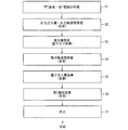
- FIG. 8 is a flowchart showing manufacturing steps of the organic EL display device 100 in the order of steps.
- the TFT substrate 110 is fabricated, and the first electrode 121 is formed on the fabricated TFT substrate 110 (step S1).
- the TFT substrate 110 can be manufactured using a known technique.
- the hole injection layer and the hole transport layer are formed on the entire surface of the pixel region by vacuum evaporation using an open mask as the evaporation mask 50.
- the hole injection layer and the hole transport layer can be the hole injection layer / hole transport layer 122 as described above.
- step S3 the light emitting layers 123R, 123G, and 123B are separately deposited by vacuum vapor deposition. Thereby, a pattern film corresponding to each of the pixels 101R, 101G, and 101B is formed.
- the electron transport layer 124, the electron injection layer 125, and the second electrode 126 are sequentially vacuumed on the TFT substrate 110 on which the light emitting layers 123R, 123G, and 123B are formed, using an open mask as a vapor deposition mask 50. It is formed over the entire pixel region by vapor deposition (steps S4 to S6).
- the region (display unit) of the organic EL element 120 is sealed so that the organic EL element 120 is not deteriorated by moisture or oxygen in the atmosphere with respect to the substrate on which the vapor deposition is completed (step S7). ).
- Sealing includes a method of forming a film that does not easily transmit moisture or oxygen by a CVD method or the like, and a method of bonding a glass substrate or the like with an adhesive or the like.
- the organic EL display device 100 is manufactured through the processes as described above.
- the organic EL display device 100 can perform desired display by causing a current to flow from the driving circuit formed outside to the organic EL element 120 in each pixel to emit light.
- FIG. 4 is a cross-sectional view showing a schematic configuration of a main part in the vacuum chamber 10 after the vapor deposition process.
- the vapor deposition material In vacuum vapor deposition, the vapor deposition material is heated and sublimated under high vacuum as described above. For this reason, the vapor deposition particles injected from the vapor deposition source 20 are scattered over a wide range in the vacuum chamber 10.
- the scattered vapor particles are attached to the in-chamber components 70 (for example, the deposition plate 30 and the shutter 40) after the vapor deposition process. It adheres and accumulates as a kimono 22.
- the material of the organic film constituting the organic EL element 120 is very expensive. For this reason, the reduction in the utilization efficiency of the organic material leads to an increase in the manufacturing cost of the organic EL display device 100 because the amount of the organic material used per one organic EL display device 100 increases.
- the collection and reuse of the vapor deposition material that has not adhered to the film formation substrate 60 is an extremely important process in the manufacture of the organic EL display device 100.
- the vapor deposition material injected from the vapor deposition source 20 adheres to the in-chamber component 70, but if it adheres to a certain extent, it peels off due to its own weight, The inside of the vacuum chamber 10 is contaminated. Therefore, it is necessary to periodically replace the in-chamber component 70 provided at the position where the vapor deposition particles adhere as described above.
- the in-chamber component 70 to which the vapor deposition particles adhere is attached to the in-chamber component 70.
- the attached deposit 22 is peeled off, collected, and reused.
- FIG. 1 are diagrams showing the separation / recovery process of the deposit 22 according to the present embodiment in the order of processes.
- the collection of the deposit 22 is performed when a preset deposition condition such as a preset number of times of vapor deposition or a deposited film thickness of the deposit 22 is reached, in other words, for example, when a preset replacement condition for the in-chamber component 70 is reached. Is called.
- the deposit 22 attached to the in-chamber component 70 is scraped off from the in-chamber component 70 to be peeled off (attachment stripping treatment, stripping step).
- the recovered material 80 recovered by scraping off from the in-chamber component 70 is scraped by the debris 71a of the layer 71 made of the material adsorbed on the magnet (that is, the layer 71 made of the material adsorbed on the magnet). Will come off).
- the method for peeling the deposit 22 from the in-chamber component 70 is not particularly limited, but dry peeling is preferable.
- various known grinding tools and cutting tools such as a so-called scraper such as a spatula, a grinder, and a polisher can be used.
- FIG. 1 shows a schematic configuration of a main part in the deposit collecting apparatus used in the present embodiment.
- the deposit collection device 200 used in the present embodiment contains contaminants (impurities) from the collected material 80 that is collected by scraping from the in-chamber component 70.
- a contaminant recovery unit 202 that separates and recovers the fragments 71a is provided.
- a conveyor 201 is provided as a conveying member that conveys the collected material 80 to the contaminant collecting unit 202.
- a magnet 202a such as an electromagnet or a magnet plate is arranged so as to be close to the conveyor 201.
- the collected material 80 passes through the magnetic field generated by the magnet 202a by being placed on the conveyor 201 and conveyed to the contaminant collecting unit 202 in a state where the magnets 202a are arranged on the conveyor 201 with a gap therebetween. (Magnetic field passing process, separation process).
- the debris 71a is made of the material adsorbed to the magnet as described above, and is adsorbed to the magnet 202a by the contaminant recovery unit 202.
- the deposit 22 that is a vapor deposition material is not attracted to the magnet 202a.
- the organic material used in the organic EL element is neither a ferromagnetic material nor a ferrimagnetic material.
- the debris 71a and the deposit 22 can be separated and recovered by passing a magnetic field as described above.
- the said magnetic field passage process is not limited to once, but can be performed in multiple times.
- the purity of the finally recovered deposit 22 that is, the final recovered material of the vapor deposition material
- the purity of the finally recovered deposit 22 can be further improved.
- vapor deposition of the organic film that is, the formation of the vapor deposition film made of the organic light emitting material
- vapor deposition is performed using a different vacuum chamber 10 for each vapor deposition process.
- the red light emitting layer 123R is formed using the vacuum chamber 10 for forming the red light emitting layer.
- the green light emitting layer 123G and the blue light emitting layer 123B are formed using the vacuum chamber 10 for forming the green light emitting layer and the vacuum chamber 10 for forming the blue light emitting layer, respectively.
- the adhesion prevention plate and the like are made of a strong substance in order to maintain the shape, when the attached deposition material is to be scraped off, it is scraped together and mixed into the peeled material as an impurity.
- the internal pressure of the chamber component may be damaged or peeled off due to water pressure. Mixed.
- it is a method of immersing a composition having a deposition material attached thereto in an organic solvent.
- a method of immersing a composition having a deposition material attached thereto in an organic solvent By using such a method, only the vapor deposition material can be dissolved and separated in an organic solvent.
- the in-chamber component 70 is formed by the layer 71 made of a material adsorbed by the magnet, and is peeled off and collected from the in-chamber component 70.
- the recovered material 80 is recovered from the recovered material 80, the debris 71a of the layer 71 made of the material adsorbed on the magnet, which is peeled together with the deposit 22 to be recovered, is passed through the magnetic field. It is only necessary to attract the magnet 202a.
- the debris 71a of the in-chamber component 70 which has been shaved during the recovery of the deposit of the vapor deposition material (that is, during the recovery of the recovered product 80), is mixed into the exfoliation of the vapor deposition material
- the debris 71a can be separated and removed from the recovered material 80.
- the step of separating and collecting the deposit 22 can be easily performed.
- the debris 71a adsorbed on the magnet 202a is a material of the in-chamber component 70, and the above-described magnetic field passing process (separation process) is a process capable of recovering this material.
- the recovery of the fragments 71a can contribute to cost reduction and prevention of environmental destruction.
- the layer 71 made of the material adsorbing the magnet and constituting the in-chamber component 70 such as the adhesion preventing plate 30 is formed of an expensive material, The material can be recovered by passing through a magnetic field as described above.
- the separation of deposits using a water jet cannot be applied to a vapor deposition material that is easily denatured by moisture.
- the present invention does not require the use of water, it can also be applied to the separation and recovery of materials that tend to be denatured by moisture.
- the present invention can easily separate the mixed impurities and obtain a high-quality vapor deposition material in consideration of damage to the in-chamber component 70.
- the types of the in-chamber components 70 to which the present invention can be applied are not limited to the deposition preventing plate 30 and the shutter 40, and can be applied to various in-chamber components 70 in the vacuum chamber 10.
- the layer 71 made of the material adsorbed by the magnet is formed at least in the portion in contact with the vapor deposition material in the in-chamber component 70 has been described as an example.
- a case where a layer made of a material that is adsorbed by a magnet is formed at least in a portion that comes into contact with a vapor deposition material in a cutting tool that scrapes off the deposit 22 from the in-chamber component 70 is taken as an example. explain.
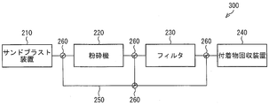
- FIG. 9 is a block diagram showing an example of the configuration of the deposit collection system used in the present embodiment.
- the deposit collection system 300 used in the present embodiment includes, for example, a sand blast device 210, a pulverizer 220, a filter 230, and a deposit collection device 240.
- a transport member 250 that transports the recovered material 80 scraped off from the surface of the object 70 to each part, and a switch 260 that switches the transport path (transport direction) are provided.
- each part will be described later together with a method for collecting and reusing the deposits attached to the in-chamber component 70.
- the deposits 22 attached to the in-chamber components 70 such as the adhesion preventing plate 30 and the shutter 40 are peeled off by a sandblast method using an abrasive made of a material adsorbed by the magnet on the above-mentioned cutting tool. To do.
- abrasives such as alumina particles, silicon carbide particles, sand, etc. having a diameter of about several hundred ⁇ m ⁇ are caused to collide with the surface of an object to be polished using air pressure. This is a method of excavating or polishing the surface of the object to be polished by the impact force at this time.
- an abrasive made of a material that is adsorbed by the magnet is used as the abrasive.
- the structure of the vapor deposition apparatus 1 used by this Embodiment is the same as Embodiment 1.
- the material of the in-chamber component 70 such as the deposition preventing plate 30 and the shutter 40 is arbitrary.
- FIG. 10 are diagrams showing a separation / recovery process of the deposit 22 according to the present embodiment.
- the sandblasting device 210 is used, and the abrasive 212 is sprayed from the nozzle 211 of the sandblasting device 210 to the deposit 22 adhered to the in-chamber component 70 (attachment stripping). Processing, peeling step).
- the collected mixture (recovered material) is conveyed to the deposit collecting device 240 by being conveyed by a conveying member 250 such as a conveyor, as in the first embodiment.
- a conveying member 250 such as a conveyor
- FIG. 10 has shown schematic structure of the principal part in the deposit
- the deposit recovery device 240 used in the present embodiment contains a mixture of the abrasive 212 and the deposit 22 peeled off from the in-chamber component 70.
- a contaminant recovery unit 241 for separating and recovering the abrasive 212 that is an object (impurity) is provided.
- the magnet collection unit 241 is provided with a magnet 241a such as an electromagnet or a magnet plate so as to be close to the transport member 250.
- the mixture (recovered material) is thus transported to the contaminant collection unit 241 by the transport member 250 in a state where the magnet 241a is disposed on the conveyor, for example, a gap on the conveyor 250, It passes through the magnetic field by the magnet 241a (magnetic field passing process, separation process).
- the abrasive 212 is made of the material adsorbed to the magnet as described above, and is adsorbed to the magnet 241a by the contaminant recovery unit 241.
- the deposit 22 that is a vapor deposition material is not attracted to the magnet 241a.
- the abrasive 212 and the deposit 22 can be separated and recovered by passing a magnetic field as described above.
- the magnetic field passing process is not limited to one time but can be performed a plurality of times.
- the purity of the finally recovered deposit 22 that is, the final recovered material of the vapor deposition material
- the purity of the finally recovered deposit 22 can be further improved.
- the filter 230 having an opening 221 having a predetermined diameter may be selectively passed and classified.
- polishing agent 212 with a large diameter which does not pass the filter 230 can be isolate
- a crushing step (milling step) for crushing 22 with a crusher 220 (mill) may be included.
- the abrasive 212 contained in the mixture (recovered material) obtained by the deposit peeling process can be used as it is as a pulverizing member.
- the deposit 22 is peeled (desorbed) from the surface of the in-chamber component 70 using the sand blast method. Therefore, the deposit 22 can be efficiently and sufficiently desorbed from the surface of the in-chamber component 70 without using an organic solvent.
- a polishing tool made of a material adsorbed by a magnet is used as a cutting tool, and the deposit 22 is scraped off from the in-chamber component 70 by a sandblast method. I gave it as an explanation.
- the present embodiment is not limited to this, and the scraper, grinder, polisher, or the like, in which a layer made of a material adsorbed by the magnet is formed at least in a portion in contact with the vapor deposition material as the above-described cutting tool. It is also possible to use other cutting tools.
- the material that is attracted to the magnet is not particularly limited as long as the material is a material that is attracted to the magnet.
- a ferromagnetic material (ferromagnetic material) and a ferrimagnetic material, which are magnetic materials having a ferromagnetic portion can be given.
- iron or stainless steel exhibiting ferromagnetism is preferably used as the material. It is done.
- the material adsorbed to the magnet and the layer made of the material should have as high a hardness as possible so that the material adsorbed on the magnet in the deposit peeling process does not desorb or denature in large quantities. It is desirable to have.
- the magnet is also used from the viewpoint of reducing the amount of desorbed material (striped material) from the layer made of the material adsorbed to the magnet. It is preferable that the layer made of the material adsorbed on and the material have as high a hardness as possible.
- a material to be used may be appropriately selected and adjusted in consideration of workability, material cost, and the like.
- the layer made of the material adsorbed on the magnet is composed of one layer in order to collect and reuse it.
- the base material layer used for the above-described cutting tool is not particularly limited, and may be composed of one layer or may have a laminated structure of two or more layers. Moreover, it may be formed of one type of material and may be formed of two or more types of materials.
- the deposit 22 is formed from the in-chamber component 70 using the cutting tool in which the layer made of the material that is adsorbed by the magnet is formed at least in the portion in contact with the vapor deposition material. Scrape off.
- the mixed tool can be obtained by passing the magnetic field as described above. Only debris can be separated and removed.
- the mixture (recovered material) scraped off from the in-chamber component 70 is simply passed through the magnetic field, so that the process of separating and recovering the deposit 22 can be performed easily.
- a high-purity vapor deposition material can be recovered and reused without adding a complicated separation process step.
- the abrasive 212 adsorbed on the magnet 241a in the magnetic field passage process can be recovered and reused. For this reason, while being able to aim at reduction of the cost increase of a simple reuse process and a reuse process, a waste can be reduced and an environmental load can be reduced.
- this embodiment mode can be used in combination with the first embodiment mode. That is, for example, a layer made of a material that is adsorbed by the magnet may be provided in at least a portion in contact with the vapor deposition material in the in-chamber component 70 and the cutting tool.
- the type of material adsorbed on the magnet may be different between the in-chamber component 70 and the cutting tool.
- FIG. 11 is a cross-sectional view showing the layer structure of the in-chamber component used in the present embodiment.
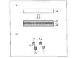
- FIGS. 12A and 12B are diagrams showing a part of the separation / recovery process of the deposit 22 according to the present embodiment.
- the in-chamber component 70 is formed on the surface of the base material 72 as a layer 71 made of a material adsorbing to the magnet, for example, a plate made of a material adsorbing to the magnet,
- the present embodiment is different from the first embodiment in that the adhesive layer 73 is attached to the substrate 72.
- the layer 71 made of the material adsorbed on the magnet for example, a plate material made of the material adsorbed on the magnet is attached to the base material 72 by the adhesive layer 73, so that FIG. As shown, the plate material to which the deposit 22 is attached can be easily peeled off from the substrate 72.
- the surface of the in-chamber component 70 in other words, the surface of the base material 72 is not damaged, and the base material 72 can be reused as it is.
- the plate material is divided and pasted into a plurality of small pieces so that it can be easily taken out of the vacuum chamber 10.
- the plate material taken out of the vacuum chamber 10 and having the adherent 22 attached to the surface is pulverized by using, for example, a pulverizer to detach the adherent 22 as shown in FIG. be able to.
- the deposit 22 can be scraped off from the surface of the plate by the method shown in the first and second embodiments.
- the mixture of the plate material fragments and the deposits 22 thus obtained can separate and remove only the plate material fragments by passing a magnetic field as shown in the first and second embodiments. .
- the present embodiment can provide the same effects as those of the first and second embodiments.
- the deposition material used for manufacturing the organic EL display device using the vacuum deposition method is collected as the collection of the deposition material used in the vacuum deposition method.
- the case of recovering the organic material has been described as an example.
- a vacuum evaporation method using a vapor deposition mask typically, as described above, there is a vacuum evaporation method using a vapor deposition mask called a shadow mask.
- the vacuum deposition method is generally used, for example, in a film forming method in an organic EL display device.
- the present embodiment is not limited to this, and the configuration in the film forming chamber of a vacuum film forming apparatus using a vacuum film forming method such as a vacuum deposition method, a sputtering method, an ion plating method, a CVD method, or the like.
- the present invention can be applied to the entire collection of film-forming materials that adhere to objects and are not attracted to magnets.
- the collected film forming material is not limited to an organic material, and may be a film forming material that can be separated from the above-described material adsorbed to the magnet due to the difference in magnetism by passing a magnetic field.
- the collected film forming material is not limited to an organic material, and may be a film forming material that can be separated from the above-described material adsorbed to the magnet due to the difference in magnetism by passing a magnetic field.
- ITO used as a conductive film material used for the first electrode 121 and the second electrode 126 in the organic EL display device 100 has a high visible light transmittance (high transparency) and an electrical resistance (specific resistance). ) Is small, and patterning by photoetching is easy, so as transparent conductive films, pixel electrodes and counter electrodes of liquid crystal panels, PDP (plasma display panels) and organic / inorganic EL electrodes, PDP electromagnetic filters, touch panels, Widely used in solar cells.
- ITO indium contained in ITO is a metal with a small amount of reserve called a rare metal, and the amount used is increasing due to a high elongation rate. Therefore, recovery and recycling are extremely important.
- a vacuum film forming method such as a sputtering method, a vacuum deposition method, or an ion plating method is often used.
- a transparent electrode made of ITO such as a liquid crystal display, is often formed into a thin film using a sputtering method.
- the method for collecting a film forming material peels off and collects the film forming material attached to the surface of the film forming jig provided in the film forming chamber in the vacuum film forming apparatus.
- a method of collecting a film forming material wherein a layer made of a material adsorbed by a magnet is provided at least in a portion of the film forming jig that contacts the film forming material, and the surface of the film forming jig
- a separation step of separating and recovering the film forming material is caused to adsorb to the magnet and from the film-forming material.
- the film forming material attached to the surface of the film forming jig is cut at least at a portion in contact with the film forming material with a cutting tool made of a material adsorbed by a magnet.
- the film forming material is peeled off in the peeling step, and in the separation step, the fragments of the tool made of the material adsorbed on the magnet mixed with the film forming material peeled in the peeling step and the peeling step are formed.
- a separation step of separating the layered material made of the material adsorbed on the magnet, which is peeled off together with the film material, onto the magnet, separating the filmed material from the filmed material, and collecting the filmed material Is preferred.
- the method for recovering a film forming material includes the film forming material attached to the surface of the film forming jig provided in the film forming chamber in the vacuum film forming apparatus.
- the film forming material is recovered by peeling off the film, and the film forming material adhering to the surface of the film forming jig is made of a material that is adsorbed by a magnet at least at a portion that contacts the film forming material. From the film forming material, adhering the debris of the cutting tool made of the material adsorbed to the magnet mixed with the film forming material peeled off by the cutting tool and the film forming material peeled in the peeling process to the magnet. A separation step of separating and recovering the film forming material.
- the debris made of the material adsorbed by the magnet which is peeled together with the film forming material when the film forming material is peeled, is adsorbed by the magnet and separated from the film forming material. Therefore, according to each of the above methods, the film forming material can be recovered efficiently and at low cost.
- the film forming material can be recovered and reused with high purity without adding a complicated separation processing step.
- the debris adsorbed on the magnet can be separated and collected in the separation step. Therefore, cost recovery and environmental destruction prevention can be achieved by collecting the fragments.
- the debris of the cutting tool is an abrasive made of a material adsorbed on a magnet
- the film forming material is adsorbed on the cutting tool by a magnet. Peeling is preferably performed by a sandblasting method using an abrasive made of a material.
- the film forming material attached to the film forming jig can be efficiently and sufficiently detached from the surface of the film forming jig.
- the method for collecting the film-forming material is a method in which the mixture of the film-forming material and the abrasive obtained in the peeling step is classified by a filter before the separation step, and the abrasive does not pass through the filter. It is preferable to further include a classification step for separating the.
- the film forming material recovery method includes a pulverizing step of pulverizing the film forming material contained in the mixture of the film forming material and the abrasive obtained in the peeling step before the classification step. It is preferable to provide.
- the film forming material can be pulverized so that the film forming material passes through the filter.
- the pulverizing step it is preferable to pulverize the film forming material using an abrasive contained in the mixture.
- the abrasive since the abrasive is contained in the mixture of the film forming material and the abrasive obtained in the peeling step, the abrasive can be used as it is as a grinding member. it can.
- the separation step it is preferable that the mixture of the film forming material and debris is passed through the magnetic field of the magnet a plurality of times.
- the material adsorbed by the magnet includes a ferromagnetic material or a ferrimagnetic material.
- the film forming material is preferably an organic material used for an organic electroluminescence element.
- Organic materials used in organic electroluminescence elements are expensive, and it is desirable to collect and reuse them.
- the organic material used in the organic electroluminescence element is not attracted to the magnet. For this reason, it can collect
- the present invention relates to a structure in which a film is attached to the surface of a film forming jig provided in a film forming chamber in a vacuum film forming apparatus using a vacuum film forming method such as a vacuum deposition method, a sputtering method, an ion plating method, or a CVD method. It can utilize suitably for collection
- a vacuum film forming method such as a vacuum deposition method, a sputtering method, an ion plating method, or a CVD method.
- Vapor deposition apparatus 10 Vacuum chamber 11 Inner wall 20 Vapor deposition source 21 Injection port 22 Deposited material (film-forming material) 30 deposition plate 31 first deposition plate 31a opening 32 second deposition plate 32a opening 40 shutter 50 mask 51 opening 60 deposition substrate 61 deposition surface 70 components in chamber 71a debris 72 base Material 73 Adhesive layer 80 Collected material 100 Organic EL display device 101R / 101G / 101B Pixel 110 TFT substrate 111 Insulating substrate 112 TFT 113 Wiring 114 Interlayer insulating film 114a Contact hole 115 Edge cover 120 Organic EL element 121 First electrode 122 Hole injection layer / hole transport layer 123R / 123G / 123B Light emitting layer 124 Electron transport layer 125 Electron injection layer 126 Second electrode 130 Adhesion Layer 140 Sealing substrate 200 Deposited material recovery device 201 Conveyor 202 Contaminant recovery unit 202a Magnet 210 Sandblasting device 211 Nozzle 212 Ab
Landscapes
- Chemical & Material Sciences (AREA)
- Engineering & Computer Science (AREA)
- Chemical Kinetics & Catalysis (AREA)
- Materials Engineering (AREA)
- Mechanical Engineering (AREA)
- Metallurgy (AREA)
- Organic Chemistry (AREA)
- Manufacturing & Machinery (AREA)
- Electroluminescent Light Sources (AREA)
- Physical Vapour Deposition (AREA)
Abstract
Description
本実施の形態にかかる成膜材料の回収方法並びに成膜材料の回収に用いられる成膜装置および回収装置について、図1の(a)~(d)乃至図8を参照して説明すれば、以下の通りである。
図5は、有機EL表示装置の概略構成を示す断面図である。
図6は、有機EL表示装置100の表示部を構成する有機EL素子120の概略構成を示す断面図である。
絶縁基板111としては、例えば、無アルカリガラスやプラスチック等を用いることができる。本実施の形態においては、板厚0.7mmの無アルカリガラスを使用した。
有機EL素子120は、低電圧直流駆動による高輝度発光が可能な発光素子であり、第1電極121、有機EL層、第2電極126が、この順に積層されている。
第1電極121は、電極材料をスパッタ法等で形成した後、フォトリソグラフィ技術およびエッチングにより、個々の画素101R・101G・101Bに対応してパターン形成されている。
図2は、本実施の形態で用いる真空蒸着装置の概略構成を示す断面図である。
ここで、真空蒸着法を用いた成膜パターンの形成方法について、主に図7および図8を用いて以下に説明する。
図8は、有機EL表示装置100の製造工程を工程順に示すフローチャートである。
図4は、蒸着工程後の真空チャンバ10内の要部の概略構成を示す断面図である。
上述したように、防着板やシャッタ等のチャンバ内構成物に付着した付着物を再利用するためには、チャンバ内構成物から付着物を脱離させる必要がある。
(1)有機溶剤を用いるので、溶剤コストがかかり、また高度な廃液設備、再処理設備が必要となる。
(2)有機溶剤が元々含有している不純物が、回収された蒸着材料に混入する。この不純物は分離が難しく、蒸着材料の昇華精製等による高純度化処理が必要となる(コスト増要因)。
(3)蒸着材料の溶解性に依存するため、回収できる蒸着材料が制限される。
(4)防着板やシャッタに対して、有機溶剤耐性を付与する必要がある。
本実施の形態について主に図9および図10の(a)~(f)に基づいて説明すれば、以下の通りである。
図9は、本実施の形態で用いられる付着物回収システムの構成の一例を示すブロック図である。
上記付着物回収システム300を用いてチャンバ内構成物70に付着した付着物22の回収・再利用を行う方法について、図10の(a)~(f)を参照して以下に説明する。
本実施の形態でも、磁石に吸着する材料としては、磁石に吸着する材質の材料であれば、特に限定されるものではない。代表的には、実施の形態1に記載したように、強磁性体部分を有する磁性材料である、強磁性体(フェロ磁性体)やフェリ磁性体が挙げられる。
本実施の形態によれば、上記したように、少なくとも蒸着材料と接触する部分に、磁石に吸着される材料からなる層が形成された削具を使用してチャンバ内構成物70から付着物22を削ぎ落とす。
なお、本実施の形態は、前記実施の形態1と組み合わせて使用することができる。すなわち、例えば、チャンバ内構成物70および削具における、少なくとも蒸着材料と接触する部分に、それぞれ、磁石に吸着される材料からなる層を設けてもよい。
本実施の形態について主に図11および図12の(a)・(b)に基づいて説明すれば、以下の通りである。
以上のように、実施の形態1~3では、真空成膜法で使用される成膜材料の回収として、真空蒸着法を用いた有機EL表示装置の製造に用いられる蒸着材料の回収を行う場合を例に挙げて説明するとともに、有機材料の回収を行う場合を例に挙げて説明した。
本発明の一態様にかかる成膜材料の回収方法は、以上のように、真空成膜装置における成膜チャンバ内に設けられた成膜治具の表面に付着した成膜材料を剥離して回収する成膜材料の回収方法であって、上記成膜治具における少なくとも上記成膜材料と接触する部分に、磁石に吸着される材料からなる層が設けられており、上記成膜治具の表面に付着した成膜材料を剥離する剥離工程と、上記剥離工程で成膜材料とともに剥離された、上記磁石に吸着される材料からなる層の破片を、磁石に吸着させて、上記成膜材料から分離して上記成膜材料を回収する分離工程とを備えている。
10 真空チャンバ
11 内壁
20 蒸着源
21 射出口
22 付着物(成膜材料)
30 防着板
31 第1の防着板
31a 開口部
32 第2の防着板
32a 開口部
40 シャッタ
50 マスク
51 開口部
60 被成膜基板
61 被成膜面
70 チャンバ内構成物
71a 破片
72 基材
73 粘着層
80 回収物
100 有機EL表示装置
101R・101G・101B 画素
110 TFT基板
111 絶縁基板
112 TFT
113 配線
114 層間絶縁膜
114a コンタクトホール
115 エッジカバー
120 有機EL素子
121 第1電極
122 正孔注入層兼正孔輸送層
123R・123G・123B 発光層
124 電子輸送層
125 電子注入層
126 第2電極
130 接着層
140 封止基板
200 付着物回収装置
201 コンベア
202 混入物回収部
202a 磁石
210 サンドブラスト装置
211 ノズル
212 研磨剤
220 粉砕機
221 開口部
230 フィルタ
240 付着物回収装置
241 混入物回収部
241a 磁石
250 搬送部材
260 切替器
300 付着物回収システム
Claims (10)
- 真空成膜装置における成膜チャンバ内に設けられた成膜治具の表面に付着した成膜材料を剥離して回収する成膜材料の回収方法であって、
上記成膜治具における少なくとも上記成膜材料と接触する部分に、磁石に吸着される材料からなる層が設けられており、
上記成膜治具の表面に付着した成膜材料を剥離する剥離工程と、
上記剥離工程で成膜材料とともに剥離された、上記磁石に吸着される材料からなる層の破片を、磁石に吸着させて、上記成膜材料から分離して上記成膜材料を回収する分離工程とを備えていることを特徴とする成膜材料の回収方法。 - 上記成膜治具の表面に付着した成膜材料を、少なくとも上記成膜材料と接触する部分が、磁石に吸着される材料からなる削具で削ることで上記剥離工程における成膜材料の剥離が行われるとともに、
上記分離工程では、上記剥離工程で剥離した成膜材料に混ざっている、磁石に吸着される材料からなる削具の破片および上記剥離工程で成膜材料とともに剥離された、上記磁石に吸着される材料からなる層の破片を、磁石に吸着させて、上記成膜材料から分離して上記成膜材料を回収する分離工程とを備えていることを特徴とする請求項1に記載の成膜材料の回収方法。 - 真空成膜装置における成膜チャンバ内に設けられた成膜治具の表面に付着した成膜材料を剥離して回収する成膜材料の回収方法であって、
上記成膜治具の表面に付着した成膜材料を、少なくとも上記成膜材料と接触する部分が、磁石に吸着される材料からなる削具で削って剥離する剥離工程と、
上記剥離工程で剥離した成膜材料に混ざっている、磁石に吸着される材料からなる削具の破片を、磁石に吸着させて、上記成膜材料から分離して上記成膜材料を回収する分離工程とを備えていることを特徴とする成膜材料の回収方法。 - 上記削具の破片が、磁石に吸着される材料からなる研磨剤であり、
上記剥離工程では、上記成膜材料を、上記削具に、磁石に吸着される材料からなる研磨剤を用いたサンドブラスト法で剥離することを特徴とする請求項2または3に記載の成膜材料の回収方法。 - 上記分離工程の前に、上記剥離工程で得られた、上記成膜材料と研磨剤との混合物を、フィルタにより分級して、フィルタを通過しない研磨剤を分離する分級工程をさらに備えていることを特徴とする請求項4に記載の成膜材料の回収方法。
- 上記分級工程の前に、上記剥離工程で得られた、上記成膜材料と研磨剤との混合物中に含まれている成膜材料を粉砕する粉砕工程を備えていることを特徴とする請求項5に記載の成膜材料の回収方法。
- 上記粉砕工程では、上記混合物中に含まれている研磨剤を用いて上記成膜材料を粉砕することを特徴とする請求項6に記載の成膜材料の回収方法。
- 上記分離工程では、上記成膜材料と破片との混合物を、上記磁石の磁界内を複数回通過させることを特徴とする請求項1~7の何れか1項に記載の成膜材料の回収方法。
- 上記磁石に吸着される材料が、強磁性体またはフェリ磁性体であることを特徴とする請求項1~8の何れか1項に記載の成膜材料の回収方法。
- 上記成膜材料が、有機エレクトロルミネッセンス素子に用いられる有機材料であることを特徴とする請求項1~9の何れか1項に記載の成膜材料の回収方法。
Priority Applications (3)
| Application Number | Priority Date | Filing Date | Title |
|---|---|---|---|
| CN201180060616.2A CN103270186B (zh) | 2010-12-23 | 2011-12-16 | 成膜材料的回收方法 |
| JP2012549771A JP5336006B2 (ja) | 2010-12-23 | 2011-12-16 | 成膜材料の回収方法 |
| US13/996,515 US8668157B2 (en) | 2010-12-23 | 2011-12-16 | Method of recovering film-forming material |
Applications Claiming Priority (2)
| Application Number | Priority Date | Filing Date | Title |
|---|---|---|---|
| JP2010286821 | 2010-12-23 | ||
| JP2010-286821 | 2010-12-23 |
Publications (1)
| Publication Number | Publication Date |
|---|---|
| WO2012086535A1 true WO2012086535A1 (ja) | 2012-06-28 |
Family
ID=46313807
Family Applications (1)
| Application Number | Title | Priority Date | Filing Date |
|---|---|---|---|
| PCT/JP2011/079151 Ceased WO2012086535A1 (ja) | 2010-12-23 | 2011-12-16 | 成膜材料の回収方法 |
Country Status (4)
| Country | Link |
|---|---|
| US (1) | US8668157B2 (ja) |
| JP (1) | JP5336006B2 (ja) |
| CN (1) | CN103270186B (ja) |
| WO (1) | WO2012086535A1 (ja) |
Cited By (1)
| Publication number | Priority date | Publication date | Assignee | Title |
|---|---|---|---|---|
| WO2024189906A1 (ja) * | 2023-03-16 | 2024-09-19 | 株式会社東芝 | 光電変換素子の製造方法 |
Families Citing this family (6)
| Publication number | Priority date | Publication date | Assignee | Title |
|---|---|---|---|---|
| CN104993070A (zh) * | 2015-07-02 | 2015-10-21 | 深圳市华星光电技术有限公司 | 一种制作柔性oled显示器件的方法 |
| CN108212429A (zh) * | 2018-02-05 | 2018-06-29 | 赣州清亦华科科技有限公司 | 一种用于稀土粉料的新式提纯装置 |
| CN111304592B (zh) * | 2020-02-21 | 2025-01-10 | 福建华佳彩有限公司 | 一种蒸镀机蒸镀材料的回收装置 |
| JP7140801B2 (ja) * | 2020-07-29 | 2022-09-21 | キヤノントッキ株式会社 | 成膜装置及び電子デバイスの製造方法 |
| CN113458609A (zh) * | 2021-05-27 | 2021-10-01 | 上海传芯半导体有限公司 | 再生掩模透光基板的处理方法及掩模基版的制造方法 |
| TWI815764B (zh) * | 2023-01-11 | 2023-09-11 | 台群國際股份有限公司 | 太陽能板回收處理分類專用機 |
Citations (14)
| Publication number | Priority date | Publication date | Assignee | Title |
|---|---|---|---|---|
| JPS62112790A (ja) * | 1985-11-09 | 1987-05-23 | Anelva Corp | 集塵装置付薄膜処理装置 |
| JPH01159368A (ja) * | 1987-12-15 | 1989-06-22 | Canon Inc | 堆積膜形成装置 |
| JPH1015826A (ja) * | 1996-06-28 | 1998-01-20 | Dainippon Printing Co Ltd | 厚膜パターン形成方法並びにパターン形成材料の選別方法及びそれに用いる選別装置 |
| JPH10284571A (ja) * | 1997-04-09 | 1998-10-23 | Nec Kyushu Ltd | 半導体装置の製造装置および製造方法 |
| JPH11229123A (ja) * | 1998-02-12 | 1999-08-24 | Casio Comput Co Ltd | 蒸着装置 |
| JP2001179629A (ja) * | 1999-12-24 | 2001-07-03 | Fuji Seisakusho:Kk | 低融点ガラスの隔壁形成方法及び装置、並びに前記方法における低融点ガラスの分離・回収方法及び低融点ガラスペーストのリサイクル方法 |
| JP2001254167A (ja) * | 2000-03-10 | 2001-09-18 | Ricoh Co Ltd | スパッタ装置の防着面清掃方法及び防着板 |
| JP2002114968A (ja) * | 2000-08-04 | 2002-04-16 | Maruo Calcium Co Ltd | 研磨材及び該研磨材を用いた研磨方法 |
| JP2002222628A (ja) * | 2001-01-26 | 2002-08-09 | Shinji Kanda | サンドブラストによるフラットパネルディスプレイの隔壁形成及び電極形成用方法、並びにこの隔壁形成方法を用いた隔壁形成材料のリサイクル方法 |
| JP2004351858A (ja) * | 2003-05-30 | 2004-12-16 | Kakihara Kogyo Kk | 金属被膜樹脂材の金属と樹脂材の分離回収方法及びその金属と樹脂分離回収装置 |
| JP2005068485A (ja) * | 2003-08-25 | 2005-03-17 | Canon Inc | 基板処理装置及び基板処理方法 |
| JP2006169573A (ja) * | 2004-12-14 | 2006-06-29 | Laser Gijutsu Sogo Kenkyusho | 蒸着マスクのクリーニング方法、蒸着マスククリーニング装置、有機el素子の製造方法、および、有機el素子の製造装置 |
| JP2007126727A (ja) * | 2005-11-07 | 2007-05-24 | Hitachi Zosen Corp | 真空蒸着用防着装置 |
| JP2007154046A (ja) * | 2005-12-05 | 2007-06-21 | Seiko Epson Corp | 研削用粉末、研削方法、フラットディスプレイパネル用基板の製造方法、フラットディスプレイパネル用基板、フラットディスプレイパネルおよび電子機器 |
Family Cites Families (8)
| Publication number | Priority date | Publication date | Assignee | Title |
|---|---|---|---|---|
| JP4059946B2 (ja) | 1996-12-06 | 2008-03-12 | 株式会社アルバック | 有機薄膜形成装置及び有機材料の再利用方法 |
| JP2002190389A (ja) | 2000-12-22 | 2002-07-05 | Nippon Steel Chem Co Ltd | 有機el素子の製造方法及び装置 |
| JP2002292346A (ja) | 2001-03-29 | 2002-10-08 | Sharp Corp | 付着膜回収装置および付着膜の回収方法 |
| JP2008088465A (ja) | 2006-09-29 | 2008-04-17 | Seiko Epson Corp | 蒸着装置および有機エレクトロルミネッセンス装置の製造方法 |
| JP2008127642A (ja) | 2006-11-22 | 2008-06-05 | Toppan Printing Co Ltd | 蒸着装置及び蒸着材料の再生方法 |
| JP2008223102A (ja) | 2007-03-14 | 2008-09-25 | Seiko Epson Corp | 蒸着装置、および蒸着方法 |
| TWI426964B (zh) * | 2008-09-17 | 2014-02-21 | 日立全球先端科技股份有限公司 | Organic EL mask cleaning device, organic EL display manufacturing device, organic EL display and organic EL mask cleaning method |
| CN101494156B (zh) * | 2009-02-19 | 2010-06-09 | 上海宏源照明电器有限公司 | 电磁感应灯及其排气管护套 |
-
2011
- 2011-12-16 CN CN201180060616.2A patent/CN103270186B/zh not_active Expired - Fee Related
- 2011-12-16 WO PCT/JP2011/079151 patent/WO2012086535A1/ja not_active Ceased
- 2011-12-16 JP JP2012549771A patent/JP5336006B2/ja not_active Expired - Fee Related
- 2011-12-16 US US13/996,515 patent/US8668157B2/en not_active Expired - Fee Related
Patent Citations (14)
| Publication number | Priority date | Publication date | Assignee | Title |
|---|---|---|---|---|
| JPS62112790A (ja) * | 1985-11-09 | 1987-05-23 | Anelva Corp | 集塵装置付薄膜処理装置 |
| JPH01159368A (ja) * | 1987-12-15 | 1989-06-22 | Canon Inc | 堆積膜形成装置 |
| JPH1015826A (ja) * | 1996-06-28 | 1998-01-20 | Dainippon Printing Co Ltd | 厚膜パターン形成方法並びにパターン形成材料の選別方法及びそれに用いる選別装置 |
| JPH10284571A (ja) * | 1997-04-09 | 1998-10-23 | Nec Kyushu Ltd | 半導体装置の製造装置および製造方法 |
| JPH11229123A (ja) * | 1998-02-12 | 1999-08-24 | Casio Comput Co Ltd | 蒸着装置 |
| JP2001179629A (ja) * | 1999-12-24 | 2001-07-03 | Fuji Seisakusho:Kk | 低融点ガラスの隔壁形成方法及び装置、並びに前記方法における低融点ガラスの分離・回収方法及び低融点ガラスペーストのリサイクル方法 |
| JP2001254167A (ja) * | 2000-03-10 | 2001-09-18 | Ricoh Co Ltd | スパッタ装置の防着面清掃方法及び防着板 |
| JP2002114968A (ja) * | 2000-08-04 | 2002-04-16 | Maruo Calcium Co Ltd | 研磨材及び該研磨材を用いた研磨方法 |
| JP2002222628A (ja) * | 2001-01-26 | 2002-08-09 | Shinji Kanda | サンドブラストによるフラットパネルディスプレイの隔壁形成及び電極形成用方法、並びにこの隔壁形成方法を用いた隔壁形成材料のリサイクル方法 |
| JP2004351858A (ja) * | 2003-05-30 | 2004-12-16 | Kakihara Kogyo Kk | 金属被膜樹脂材の金属と樹脂材の分離回収方法及びその金属と樹脂分離回収装置 |
| JP2005068485A (ja) * | 2003-08-25 | 2005-03-17 | Canon Inc | 基板処理装置及び基板処理方法 |
| JP2006169573A (ja) * | 2004-12-14 | 2006-06-29 | Laser Gijutsu Sogo Kenkyusho | 蒸着マスクのクリーニング方法、蒸着マスククリーニング装置、有機el素子の製造方法、および、有機el素子の製造装置 |
| JP2007126727A (ja) * | 2005-11-07 | 2007-05-24 | Hitachi Zosen Corp | 真空蒸着用防着装置 |
| JP2007154046A (ja) * | 2005-12-05 | 2007-06-21 | Seiko Epson Corp | 研削用粉末、研削方法、フラットディスプレイパネル用基板の製造方法、フラットディスプレイパネル用基板、フラットディスプレイパネルおよび電子機器 |
Cited By (1)
| Publication number | Priority date | Publication date | Assignee | Title |
|---|---|---|---|---|
| WO2024189906A1 (ja) * | 2023-03-16 | 2024-09-19 | 株式会社東芝 | 光電変換素子の製造方法 |
Also Published As
| Publication number | Publication date |
|---|---|
| JPWO2012086535A1 (ja) | 2014-05-22 |
| CN103270186A (zh) | 2013-08-28 |
| JP5336006B2 (ja) | 2013-11-06 |
| US8668157B2 (en) | 2014-03-11 |
| US20130292501A1 (en) | 2013-11-07 |
| CN103270186B (zh) | 2015-01-14 |
Similar Documents
| Publication | Publication Date | Title |
|---|---|---|
| JP5336006B2 (ja) | 成膜材料の回収方法 | |
| US9365927B2 (en) | Deposition method and collection method | |
| JP5285187B2 (ja) | 蒸着装置及び蒸着方法 | |
| KR100995109B1 (ko) | 제조장치 | |
| JP5373221B2 (ja) | 蒸着粒子射出装置および蒸着装置並びに蒸着方法 | |
| JP5324010B2 (ja) | 蒸着粒子射出装置および蒸着装置並びに蒸着方法 | |
| US9893283B2 (en) | Vapor deposition device, vapor deposition method, and organic electroluminescence element manufacturing method | |
| JPWO2012121139A1 (ja) | 蒸着装置及び蒸着方法 | |
| US9614155B2 (en) | Vapor deposition apparatus, vapor deposition method, and method for producing organic electroluminescent element | |
| US20170222185A1 (en) | Organic electroluminescent display substrate, organic electroluminescent display apparatus, and method for manufacturing organic electroluminescent display apparatus | |
| JP2013057108A (ja) | 多元スパッタリング装置 | |
| JP2003313655A (ja) | 製造装置 | |
| KR100984965B1 (ko) | 스퍼터링 장치 및 성막 방법 | |
| WO2012090772A1 (ja) | 蒸着装置、削具および蒸着材料の回収方法 | |
| TWI343419B (en) | Target backing plate for sputtering system | |
| JP2004277799A (ja) | 成膜装置およびそのクリーニング方法 | |
| JP4423589B2 (ja) | スパッタ装置、スパッタ方法、有機el発光素子の製造装置および有機el発光素子の製造方法 | |
| JPWO2018189906A1 (ja) | 有機el表示装置の製造方法及び製造装置 | |
| JP5478324B2 (ja) | クリーニング装置、成膜装置、成膜方法 | |
| KR20060027280A (ko) | 대향 타겟식 스퍼터링 장치 및 이를 이용한 유기 전계발광 표시 장치의 제조 방법 | |
| JP2009161819A (ja) | スパッタリング装置 | |
| JP2008053137A (ja) | 有機el素子及びこれの製造装置並びに有機el素子の製造方法 |
Legal Events
| Date | Code | Title | Description |
|---|---|---|---|
| 121 | Ep: the epo has been informed by wipo that ep was designated in this application |
Ref document number: 11850161 Country of ref document: EP Kind code of ref document: A1 |
|
| ENP | Entry into the national phase |
Ref document number: 2012549771 Country of ref document: JP Kind code of ref document: A |
|
| WWE | Wipo information: entry into national phase |
Ref document number: 13996515 Country of ref document: US |
|
| NENP | Non-entry into the national phase |
Ref country code: DE |
|
| 122 | Ep: pct application non-entry in european phase |
Ref document number: 11850161 Country of ref document: EP Kind code of ref document: A1 |