WO2012081338A1 - 欠陥検査方法及びその装置 - Google Patents
欠陥検査方法及びその装置 Download PDFInfo
- Publication number
- WO2012081338A1 WO2012081338A1 PCT/JP2011/075758 JP2011075758W WO2012081338A1 WO 2012081338 A1 WO2012081338 A1 WO 2012081338A1 JP 2011075758 W JP2011075758 W JP 2011075758W WO 2012081338 A1 WO2012081338 A1 WO 2012081338A1
- Authority
- WO
- WIPO (PCT)
- Prior art keywords
- light
- sample
- detection
- condensing
- stage
- Prior art date
- Legal status (The legal status is an assumption and is not a legal conclusion. Google has not performed a legal analysis and makes no representation as to the accuracy of the status listed.)
- Ceased
Links
Images













Classifications
-
- G—PHYSICS
- G01—MEASURING; TESTING
- G01N—INVESTIGATING OR ANALYSING MATERIALS BY DETERMINING THEIR CHEMICAL OR PHYSICAL PROPERTIES
- G01N21/00—Investigating or analysing materials by the use of optical means, i.e. using sub-millimetre waves, infrared, visible or ultraviolet light
-
- G—PHYSICS
- G01—MEASURING; TESTING
- G01N—INVESTIGATING OR ANALYSING MATERIALS BY DETERMINING THEIR CHEMICAL OR PHYSICAL PROPERTIES
- G01N21/00—Investigating or analysing materials by the use of optical means, i.e. using sub-millimetre waves, infrared, visible or ultraviolet light
- G01N21/84—Systems specially adapted for particular applications
- G01N21/88—Investigating the presence of flaws or contamination
- G01N21/95—Investigating the presence of flaws or contamination characterised by the material or shape of the object to be examined
- G01N21/956—Inspecting patterns on the surface of objects
-
- G—PHYSICS
- G01—MEASURING; TESTING
- G01N—INVESTIGATING OR ANALYSING MATERIALS BY DETERMINING THEIR CHEMICAL OR PHYSICAL PROPERTIES
- G01N21/00—Investigating or analysing materials by the use of optical means, i.e. using sub-millimetre waves, infrared, visible or ultraviolet light
- G01N21/84—Systems specially adapted for particular applications
- G01N21/88—Investigating the presence of flaws or contamination
- G01N21/8851—Scan or image signal processing specially adapted therefor, e.g. for scan signal adjustment, for detecting different kinds of defects, for compensating for structures, markings, edges
-
- G—PHYSICS
- G01—MEASURING; TESTING
- G01N—INVESTIGATING OR ANALYSING MATERIALS BY DETERMINING THEIR CHEMICAL OR PHYSICAL PROPERTIES
- G01N21/00—Investigating or analysing materials by the use of optical means, i.e. using sub-millimetre waves, infrared, visible or ultraviolet light
- G01N21/84—Systems specially adapted for particular applications
- G01N21/88—Investigating the presence of flaws or contamination
- G01N21/95—Investigating the presence of flaws or contamination characterised by the material or shape of the object to be examined
- G01N21/9501—Semiconductor wafers
-
- G—PHYSICS
- G01—MEASURING; TESTING
- G01N—INVESTIGATING OR ANALYSING MATERIALS BY DETERMINING THEIR CHEMICAL OR PHYSICAL PROPERTIES
- G01N21/00—Investigating or analysing materials by the use of optical means, i.e. using sub-millimetre waves, infrared, visible or ultraviolet light
- G01N21/84—Systems specially adapted for particular applications
- G01N21/88—Investigating the presence of flaws or contamination
- G01N21/8851—Scan or image signal processing specially adapted therefor, e.g. for scan signal adjustment, for detecting different kinds of defects, for compensating for structures, markings, edges
- G01N2021/8896—Circuits specially adapted for system specific signal conditioning
Definitions
- the present invention relates to a method and an apparatus for detecting a minute defect generated in a sample, and in particular, a defect inspection suitable for detecting a minute defect generated on a semiconductor wafer having a fine pattern formed on the surface.
- the present invention relates to a method and apparatus.
- the pattern shape formed on the wafer becomes a multilayer structure as well as finer, the number of production processes is steadily increasing.
- the fine pattern is reliably formed by inspecting the wafer on which the pattern is formed. It is important to confirm that no defects such as foreign matter have occurred.
- an optical pattern inspection apparatus (bright field pattern inspection apparatus) using a bright field
- an optical defect inspection apparatus (dark field defect inspection apparatus) using a dark field.
- a dark-field inspection apparatus has a feature of high throughput testing compared with brightfield pattern inspection apparatus.
- Patent Literature 1 and Patent Literature 2 irradiate a wafer with linear illumination light narrowed in one direction obliquely, and the wafer is perpendicular to the longitudinal direction of the linear illumination light.
- the light scattered from the surface of the wafer by linear illumination light while continuously moving in the direction to be detected is detected by the detection system above the wafer and the detection systems arranged on both sides of the wafer, and the respective detection signals are used for the wafer. It describes the detection of defects in the shape.
- Patent Document 3 uses a TDI (Time Delay Integration) sensor as a detection system, controls the line rate of the TDI sensor and the stage scan speed asynchronously, and linearly narrows the non-inspection object.
- the scattered pixel light is received only by an arbitrary pixel line of the TDI sensor, and the aspect ratio of the detected pixel size can be controlled by the speed ratio between the line rate of the TDI sensor and the stage scan speed. By doing so, it is described that auditing can be performed at a scanning speed higher than the line rate of the TDI sensor.
- TDI Time Delay Integration
- a method of separating and detecting the scattering direction using different scattering characteristics depending on the types of defects can be considered.
- detectors are placed at multiple locations, and the signals detected at each location are processed and integrated to detect scattered light from fine defects that would be buried in noise when detected from one direction.
- the detected signal can be revealed and the types of detected defects can be classified more finely.
- Patent Documents 1 and 2 Such detection of scattered light from a defect by arranging detectors in a plurality of directions is described in Patent Documents 1 and 2.
- a plurality of detectors are arranged in directions oblique to the normal direction of the substrate.
- the substrate is irradiated with linear illumination light, and the stage on which the substrate is mounted is moved at a constant speed in a direction perpendicular to the longitudinal direction of the linear illumination. Scattered light from the substrate is detected.
- position fluctuations such as pitching (vertical fluctuation) and yawing (horizontal fluctuation) occur on the table.
- the position on the substrate surface detected by the detectors arranged in different azimuth directions is displaced, and the same pattern formed on the substrate surface is detected.
- the signals detected by the respective detectors are displaced from each other. This becomes prominent when a finer defect of about several tens of nm or less is detected.
- Patent Documents 3 and 4 do not describe that a plurality of detectors are arranged in different azimuth directions to detect defects on the substrate.
- a stage means that can place a sample and move in at least one direction, and a normal direction of a surface on which the sample of the stage is placed on the sample placed on the stage means condensing a light irradiating means for irradiating light molded from a direction inclined to the linear light light formed into a linear shape is reflected and scattered in a first direction from the sample irradiated by the light irradiating means with respect to a first focusing detection means for detecting by light, from a sample irradiated with light molded linearized by light irradiation means second detecting condenses the light reflected and scattered in the second direction Condensation detection means, processing means for processing the detection signal output from the first light collection detection means and the detection signal output from the second light detection means to detect a sample-like defect, and stage means , Light irradiation means, first light detection means, second light detection means and processing In the inspection apparatus provided with the
- the deviation of the focal position of the second light collection detection means with respect to the surface of the sample is obtained, and the deviation of the focal position of the first light collection detection means obtained and the second
- the detection signal output from the first condensing detection unit and the detection signal output from the second condensing detection unit are corrected in accordance with the shift of the focal position of the condensing detection unit, and the corrected first signal is corrected.
- Detection signal output from the light collection detection means and the second light collection detection And to detect defects on the specimen by integrating the detection signal output from the stage.
- a stage means on which a sample can be placed and moved in at least one direction, and a surface method for placing the sample on the stage on the sample placed on the stage means
- a first condensing detection means for condensing and detecting light, and a light that is reflected and scattered in the second direction from the sample irradiated with light shaped linearly by the light irradiating means.
- Two condensing detection means a processing means for detecting a sample-like defect by processing the detection signal output from the first condensing detection means and the detection signal output from the second light detection means; Stage means, light irradiation means, first light detection means, and second light detection means;
- the first light collection detection means and the second light collection detection means each include a photoelectric converter provided with a plurality of rows of photosensor arrays, The control means controls the stage means to continuously move the stage means in one direction, and controls the photoelectric converter of the first condensing detection means and the photoelectric converter of the second condensing detection means.
- the reflected and scattered light from the sample irradiated with light shaped linearly by the light irradiation means is detected in synchronization with the movement of the stage means, and the control means further controls the processing means to control the first light collection detection means.
- the detection signal output from the photoelectric converter and the photoelectric converter of the second light collecting detection means is processed at a timing different from the motive for the movement of the stage means, and the first processed at a timing different from this synchronization.
- Condensation detection means photoelectric converter and second And to detect the sample-like defects in the integrated detection signal outputted from the photoelectric converter of the focusing detection means.
- the defect inspection method is such that the stage moves from a direction inclined with respect to the normal direction of the surface of the sample while moving the stage on which the sample is placed in one direction.
- Light shaped into a long line in a direction perpendicular to one direction is irradiated onto the surface of the sample, and the light reflected and scattered in the first direction from the surface of the sample irradiated with this linearly shaped light is collected.
- the light that has been reflected and scattered in the second direction from the surface of the sample irradiated with the linearly shaped light is collected by the first condensing detection means having a plurality of photosensor arrays.
- the second condensing detection means having a plurality of rows of optical sensor arrays detects the second condensing detection means, and the detection signals from the plurality of rows of optical sensor arrays output from the first condensing detection means are used to detect the first surface of the sample.
- Finding the deviation of the focal position of the first condensing detection means and detecting the second condensing The deviation of the focal position of the second condensing detection means with respect to the surface of the sample is obtained using the detection signals from the optical sensor arrays in a plurality of rows output from the stage, and the obtained focal position of the first condensing detection means is obtained.
- the corrected detection signal output from the first light collection detection means and the detection signal output from the second light collection detection means are integrated to detect a defect on the sample.
- the stage is moved from a direction inclined with respect to the normal direction of the surface of the sample while moving the stage on which the sample is placed in one direction.
- the surface of the sample is irradiated with light shaped into a long line in a direction perpendicular to one direction, and the light reflected and scattered in the first direction from the surface of the sample irradiated with the linearly shaped light is collected.
- the photoelectric converter of the first condensing detection means having a photoelectric converter having a light sensor array of rows, the light formed into a linear shape is irradiated and move to the direction of the stage in the second focusing detecting means having a photoelectric converter having a light sensor array of rows from the surface of the sample condenses the light reflected and scattered in the second direction Synchronously detecting, the photoelectric converter of the first condensing detection means and the second
- the detection signal output from the photoelectric converter of the light detection means is processed at a timing different from the synchronization with the movement of the stage, and the photoelectric converter of the first condensing detection means processed at a timing different from the synchronization.
- the detection signal output from the photoelectric converter of the second condensing detection means is integrated to detect a defect on the sample.
- detection signals from a plurality of detectors can be integrated and processed without being affected by fluctuations in the height direction of the substrate being inspected, and finer defects can be detected. Can now.
- Example 1 of this invention It is a block diagram explaining the principle of Example 1 of this invention. It is a top view which shows the schematic structure of the optical system of Example 1 of this invention. It is a front view which shows the schematic structure of the optical system of Example 1 of this invention. It is a front view which shows the schematic structure of the illumination optical system of Example 1 of this invention. It is a front view which shows the schematic structure of the detection optical system of Example 1 of this invention. It is a block diagram of a detection optical system for explaining a shift of a detection position on a sensor due to an AF shift. It is a block diagram which shows the structure of the image processing means which concerns on Example 1 of this invention.
- FIG. 2 is a plan view of a wafer and an enlarged view of chips formed on the wafer.
- FIG. 5 is a block diagram of a detection optical system for explaining detection position shifts caused by AF shifts on an obliquely arranged sensor. It is a graph which shows PSF of a detection system when the beam profile and pixel size of linear illumination light are considered. It is sectional drawing of the semiconductor wafer in which the pattern was formed.
- Example 2 is a block diagram of a detection optical system showing a relationship between sensors arranged obliquely and reflected / scattered light from a material in Example 1 of the present invention. It is a graph which shows the relationship between the beam profile of the linear illumination light in Example 1 of this invention, and PSF of an illumination system. It is a graph which shows the relationship between the beam profile of the linear illumination light in Example 1 of this invention, and PSF as a system which correct
- Example 2 of this invention It is a block diagram which shows the structure of the height deviation information calculation part in Example 1 of this invention. It is a block diagram explaining the principle of Example 2 of this invention. It is a graph which shows the beam profile of the linear illumination light in Example 2 of this invention, and PSF for every pixel column of a TDI sensor. It is a graph which shows PSF as a system which shifted the beam profile of the linear illumination light in Example 2 of this invention, and the output of the pixel of the TDI sensor by predetermined amount, and added together. It is a graph which shows the output of a TDI sensor when the reflected and scattered light from the repetitive pattern on a sample is detected when there is AF deviation in Example 2 of the present invention.
- Example 2 of this invention It is a block diagram which shows the structure of the image processing means which concerns on Example 2 of this invention. It is the figure which plotted arrangement
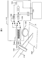
- FIG. 1 is a diagram for explaining the principle of this embodiment.
- the illumination light 116 is focused in one direction by the lens unit 101 and shaped to be parallel light in a direction perpendicular thereto, and the surface of the sample 150 on which a fine pattern is formed is irradiated from an oblique direction. To do.
- the sample 150 is moved at a constant speed in the direction of the arrow by the stage means described later.
- Reference numeral 102 denotes a detection optical system that collects light reflected / scattered in the direction of the detection optical system 102 out of the reflected / scattered light from the sample 150 irradiated with the linearly shaped illumination light 116.
- An image of the linearly irradiated region of the sample 150 is formed on the 115 detection element arrays 104 and 105.
- the detector 115 includes detection element arrays 104 and 105, a two-stage sensor (two-dimensional CCD or dual-line sensor) 103 including lead-out registers 106 and 107 for reading out signals from each of the detector elements 104 and 105, and a sample 150.
- a two-stage sensor two-dimensional CCD or dual-line sensor
- the adders 113 and 112 that add and output the height of the sample 150 are obtained using the output signal from the A / D converter 109 and the output signal from the A / D converter 110 to obtain information on the height deviation of the sample 150. This is a deviation information calculation unit.
- An image processing unit 114 detects a defect on the sample 150 in response to an output signal from the detector 115.
- FIG. 2 is a plan view showing the configuration of the optical system of the defect inspection apparatus according to the present embodiment.
- the optical system of the defect inspection apparatus according to the present embodiment includes a light source 206 on the side of the illumination optical system, and a lens unit 101 that shapes the illumination light 116 emitted from the light source 206 into a linear beam.
- the light source 206 emits an ultraviolet laser such as UV light or DUV light.
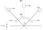
- the detection optical system 102 includes a first oblique detection optical system 102A and a first detector 115A, an upper detection optical system 102B and an upper detector 115B, a second oblique detection optical system 102C, and a second detection. 115C. Output signals from the first detector 115A, the upper detector 115B, and the second detector 115C are input to the image processing unit 114 and processed.
- the defect inspection apparatus includes a height detection unit that detects the height of the surface of the sample 150.
- the height detection unit includes a light source unit 201 that emits a plurality of linear light patterns 207, and a linear light pattern 207 emitted from the light source unit 201 from a direction inclined with respect to the normal direction of the sample 150.
- a condensing lens 202 that condenses and irradiates the surface of 150
- a condensing lens 203 that condenses reflected light (regular reflection light) from the sample 150 irradiated with a plurality of linear light patterns 207, and is condensed.
- a height detector 205 for extracting height information of the sample 150 by receiving and processing a signal obtained by detecting the reflected light from the sample 150 by the photodetector. Yes.
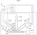
- FIG. 3A is a front view showing the configuration of the inspection optical system 100 of the defect inspection apparatus according to the present embodiment.
- the sample 150 is placed on the Z stage 303.
- the first oblique detection optical system 102A, the upper detection optical system 102B, and the second oblique detection optical system 102C are respectively an objective lens 1021 and a spatial filter 1022 as shown in FIG. 3C.
- the spatial filter 1022 shields a diffracted light pattern generated by diffracted light generated by irradiating light on a fine repeating pattern on the sample 105 with a spatial filter 1022.
- the reflected / scattered light that has passed through is imaged on the detection surface of the detector 115 by the imaging lens 1025. Since the configuration shown in FIG. 3C is common to the first oblique detection optical system 102A, the upper detection optical system 102B, and the second oblique detection optical system 102C, the last A, B, C of each component is used. The notation of the
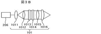
- FIG. 3B shows the configuration of the illumination optical system side.
- the illumination optical system includes a light source 206 that emits a laser beam and a lens unit 101.
- the lens unit 101 includes a beam expander 1011 for expanding the diameter of the laser beam emitted from the light source 206, a collimator lens 1012 for converting the laser whose diameter has been increased to parallel light, and polarization for adjusting the polarization state of the laser.
- a cylindrical lens 1016 is formed.
- An overall control unit 301 controls the light source 206 on the illumination side, the light source unit 201 of the height detection unit, and the stage control unit 302, and inspects the sample 150 by receiving the outputs of the image processing unit 114 and the height detection unit 205. The result is output.
- the X stage 304 is controlled by the stage control means 302 at the time of inspection to move in one direction at a constant speed, and in synchronization with the movement of the X stage 304, the first detector 115A. Detection signals are output from the upper detector 115B and the second detector 115C.
- the Y stage is controlled by the stage control means 302 to move the inspection region of the sample 150 to the adjacent inspection region.
- the X stage 304 is controlled by the stage control means 302 and moved in a direction opposite to the entire circuit ( ⁇ X direction) at a constant speed. By repeating this, the entire surface of the sample 150 can be inspected.
- the X stage 304 variations in the vertical height called pitting occurs.
- the height variation in the vertical direction also occurs due to the two-dimensional strain of the sample.
- the sample is incident on the first oblique detection optical system 102A and the second oblique detection optical system 102C 0.99
- the incident angle of the reflected / scattered light from the surface of the sample 150 changes, and the reflected / scattered light from the surface of the sample 150 is received on the respective light receiving surfaces of the first detector 115A and the second detector 115C. Misalignment occurs.
- the overall control unit 301 controls the stage based on the height information of the surface of the sample 150 detected by the height detection unit configured by the height detection unit 205 from the light source unit 201 shown in FIG.
- the position (height) is adjusted in the Z-axis direction of the Z stage 303 by controlling the means 302, but the deviation in the height direction (AF (Auto-Focus) shift) is caused by the offset of adjustment or time delay. ) Will occur. If the signals from the respective detectors are integrated and processed with the AF deviation still occurring, the image will be blurred by the amount of the AF deviation, and as a result, the accuracy of defect detection will be degraded. .
- FIG. 5 is a block diagram illustrating a configuration of the image processing unit 114.
- two signals 509A are obtained by adding the outputs of the two detection element arrays 104 and 105 output from the adder 113.
- One of them is input to the buffer memory 501A.
- Reference numeral 501A denotes a FIFO type buffer memory, which outputs an image shifted by an integral multiple of the die. Of these, noise can be reduced by superimposing images shifted by a plurality of dies.
- Reference numeral 511A denotes a first alignment processing unit that detects a positional shift between images that are an integral multiple of the die, outputs the two branched images without any positional shift, and inputs the result to the differentiator 502A.
- a signal that has been previously input to the buffer memory 501A and having detected the pattern of the same shape on the sample 150 or a signal that has detected the pattern of the same region of the adjacent die on the sample 150 is used as a reference signal and The difference is calculated (cell comparison or die comparison), and the calculated difference image signal 503A is input to the second alignment circuit unit 504A.
- the output signal 510A from the height deviation information calculation unit 112 is also input to the alignment circuit unit 504A and has a height higher than the differential image signal 503A input separately. The deviation is corrected and an image of a defect candidate is extracted.
- the signals output from the upper detector 115B and the second detector 115C in synchronization with the movement of the X stage 304 in the X direction are processed, and the heights are obtained by the alignment circuit units 504B and 504C.
- Difference images 505 ⁇ / b> B and 505 ⁇ / b> C (defect candidate images) whose deviations are corrected are extracted and input to the integrated determination unit 506.
- the integration determination unit 506 integrates the difference images 505A to 505C (defect candidate images) corrected for height deviation to generate one image.
- the image generated by the integrated determination unit 506 is compared with the threshold value by the threshold value determination unit 507, and the defect signal 508 extracted as a result of the comparison is output to the overall control unit 301.
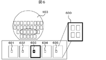
- FIG. 6 visually shows the die comparison executed by the differentiators 502A to 502C.
- a plurality of die ridges (chips) 600 are formed on a semiconductor wafer as the sample 150, and patterns 601 to 605 having the same shape are formed at corresponding locations of the dies.
- a difference image between the two images is calculated by using, as a reference image, an image of the die pattern 603 and an image of the die pattern 604 formed on a chip adjacent to the chip on which the die pattern 603 is formed. .
- each difference image output from each alignment circuit unit 504A to 504C is extracted from each defect candidate image output from each alignment circuit unit 504A to 504C executed by the integration determination unit 506.
- An example of plotting the image feature values in a three-dimensional space is shown.
- the image feature amount of the defect candidate is plotted in the three-dimensional space in this way, the feature amount of the image of the portion that is not a true defect is distributed in the center, but the feature amount of the image including the defect is a normal portion. It exists in the part away from the distribution of the difference image calculated from the image. Therefore, true defects can be detected by integrating defect candidate images obtained from the respective detectors and plotting them in a multidimensional space as shown in FIG. 7 to extract outliers.
- defect candidates obtained from the respective detectors need to be aligned.
- FIG. 8 is a graph in which an illumination profile 801 and a detection system profile 802 are plotted with respect to the stage scanning direction.
- the illumination profile 801 it is assumed that the beam width is 1.8 ⁇ m, the illumination is oblique illumination, and the illumination intensity has a Gaussian distribution.
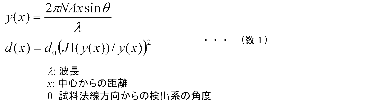
- the detection system profile 802 the detector pixel size is set to be infinitely small and installed in a direction inclined 45 degrees with respect to the normal direction of the sample, and NA (Numerical Aperture) is 0. .5, for example, assuming that scattered light due to Fraunhofer diffraction is generated from the pattern on the sample 150, the point distribution function (Point Spread Function: PSF) of the detection system is assumed. ) D (x) was determined by (Equation 1).
- the illumination of the oblique illumination system is relatively wide when compared with the PSF of the detection system, and sufficient image resolution cannot be obtained only with the illumination system in the stage scanning direction. Is shown. In order to improve the resolution of the entire apparatus, it is effective to improve the resolution of the detection system.
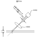
- the sample 150 is the height variation of the surface of the continuously moving to the sample 150 in the X direction, the deviation of ⁇ 0.5 [mu] m is assumed to have occurred as AF deviation as shown in FIG. 9A,
- the PSF of the detection system at this time is obtained by convolution integration of the pixel size and the PSF of the detection system represented by (Equation 1) as represented by (Equation 2), and has characteristics as shown in FIG. 9B. .
- the resolution of the detection system is worse than that of the illumination type. That is, from the graph of FIG. 9B, when a detector having a finite pixel size is used with a simple configuration as shown in FIG. 9A, the resolution in the line width direction of the illumination light beam (stage movement direction) Is determined by the resolution of the lighting system.
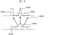
- a fine pattern 1004 is formed in a lower layer, and an optically transparent thin film 1002 such as a silicon dioxide (SiO 2) film or a silicon nitride (SiN) film is formed on the surface.
- An example in which a pattern 1007 is formed is shown.
- the sample 150 having such a cross-sectional structure is irradiated with illumination light having a beam profile such as 1001, the illumination light passes through the optically transparent film 1002 and is reflected and scattered by the fine pattern 1004 below.
- the light having a beam profile as indicated by 1003 is transmitted through the optically transparent film 1002, and this and the incident light are buffered, resulting in a distribution characteristic as indicated by 1008.
- the resolution of the illumination system is apparently lowered.
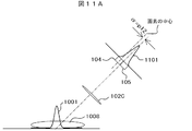
- FIG. 11A shows the same configuration as that shown in FIG. 9A, in which two pixels 104 and 105 are arranged and their size is 1.25 ⁇ m, which is half that of FIG. 9A. This shows a state in which the illumination light irradiation area on the sample 150 and the position of the detection system pixel are adjusted so that the center of the beam irradiated to the sample 150 is projected between the two pixels 104 and 105. .
- FIG. 11B shows the beam profile of illumination light and the distribution of reflected / scattered light detected by the pixels 104 and 105 in the configuration shown in FIG. 11A.
- the multi-stage line sensor is a normal multi-stage. Similar to the case of detection by a line sensor (for example, a TDI sensor (Time Delay Integration sensor)), the shift amount may be halved of the pixel size, but the beam profile 1101 is narrowed down to narrow the width of the illumination light. Is made steeper, the shift amount is not determined by the pixel size, but is determined by the beam profile of the illumination light and the resolution of the detection system, and is expressed as (Equation 6).
- TDI sensors used the shift amount represented by the s whereas a half of a pixel size, in the case where a configuration of the present invention, s is smaller than half the pixel size. This is almost equivalent to a reduction in the pixel size as a system, and a high resolution can be obtained even when a large pixel size is used. In this state, as in the case of using a general TDI sensor, the image resolution deteriorates when the movement amount is moved by an amount equal to the pixel size on the sample.
- FIG. 11C the distribution of the reflected and scattered light detected at each pixel 104 and 105, and controlled by simply staggered (overall control unit 301 shift amount from the center determined on the basis of the equation (6), X PSF as a system as a result of addition (with a time delay with respect to the synchronization signal for detecting reflected / scattered light from the sample 150 of the multi-stage line sensor 103 in synchronization with the movement of the stage 304 in the X direction) Is shown as a graph representing the beam profile of the illumination light. From this result, it can be seen that the resolution of the detection system is greatly improved compared to the case shown in FIG. 9B.
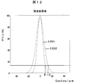
- FIG. 12 shows the characteristics of the resolution achieved by thinning the illumination light, and the resolution when the resolution of the detection system is improved by using the two-stage line sensor according to the present embodiment for the thinned illumination light.
- the graph which displayed the characteristic and superimposed is shown. It can be seen that the resolution is improved by adopting the detection system using the two-stage line sensor according to the present embodiment.
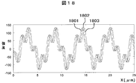
- FIG. 13A shows a simulation of sensor output with and without AF deviation when a test pattern is illuminated with a thin line using a two-stage line sensor as shown in FIG. 11A. Shows the results obtained.
- the sensor output 1302 when there is no AF deviation, the sensor output 1301 when the AF deviation of ⁇ 0.5 ⁇ m occurs, and the sensor output when the AF deviation of +0.5 ⁇ m occurs are shown by simulation results. . It can be seen that the detection signal varies greatly due to the occurrence of AF deviation.
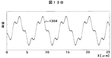
- FIG 13B contrast, obtained by simulation of the sensor output when the same AF deviation as in Figure 13A occurs with such a hammering using a detection system of a conventional pixel size 2.5 ⁇ m shown in FIG. 9A The results are shown.
- the size of the pixel is large enough to cover the fluctuation amount of the beam position due to the AF deviation, the detected pattern position does not change even if the AF deviation occurs.
- the sensitivity of defect detection becomes lower than that in the case of FIG. 13A.
- FIG. 14A shows output waveforms from the pixel rows 104 and 105 of the two-stage sensor 103 when an AF shift occurs.
- the irradiation region of the illumination light on the sample 150 and the detection system so that the center of the beam irradiated on the sample 150 is projected in the middle of the two pixels 104 and 105 without any AF deviation.
- the position of the pixel is adjusted.
- the center position of the beam on the sensor surface shifts. Therefore, the output level of the signal 1401 output from the pixel column 104 of the two-stage sensor 103 and the pixel column 105
- the level of the output signal 1402 changes. This change in signal level corresponds to the AF deviation amount.
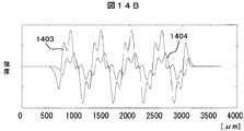
- FIG. 14B shows from the pixel row 104 when the two-stage sensor 103 detects reflected / scattered light from a repetitive pattern formed on the sample 150 when the X stage 304 is scanned in a state where AF deviation has occurred.
- the output waveform 1403 and the output waveform 1404 from the pixel column 105 are shown.
- the output signal from the pixel column 104 and the output signal from the pixel column 105 are distributed over a certain scanning range of the X stage 304.
- the height deviation information calculation unit 112 shown in FIG. 1 executes the addition of the output signal from the pixel row 104 and the output signal from the pixel row 105 over a certain scanning range of the X stage 304.
- FIG. 15 shows the configuration of the height deviation information calculation unit 112.
- Reference numerals 1503 and 1504 denote signal adders, respectively.
- the signal adder 1503 adds the signal 1501 output from the A / D converter 109 when the X stage 304 is moving in one direction at a constant speed.
- a signal adder 1504 adds the signal 1502 output from the / D converter 110.
- the addition signals output from the signal adder 1503 and the signal adder 1504 are respectively input to the processing unit 1505 and are normalized by dividing the signal value from the signal adder 1503 by the signal value from the signal adder 1504. Is done.
- the result of normalization by the processing unit 1505 is compared with data of a lookup table (LUT) in which the comparison unit 1506 compares the preset AF deviation amount and the normalized value and records the values. The amount of deviation is determined.
- LUT lookup table
- AF deviation amount information 510A to 510C obtained by the height deviation information calculation unit 112 is sent to the image processing unit 114, and the registration units 504A to 504C receive the difference information from the difference units 502A to 502C.
- Each of the output difference images 503A to 503C is corrected for the height shift by using the information of the AF shift amount.
- the height shifts detected by 510A and 510C coincide in principle. Therefore, if the average of the height deviation amounts detected by 510A and 510C is calculated and input to 504A and 504C, and this is used, the AF deviation amount can be calculated more stably.
- 510B and 504B may be omitted from FIG.
- the difference images 505A to 505C that have been corrected for the height deviation are sent to the integration determining unit 506 and integrated to generate a three-dimensional vector image.
- the image generated by the integrated determination unit 506 is sent to the threshold determination unit 507, and image feature amounts are extracted for each defect candidate, and defect candidates plotted in the three-dimensional space as described with reference to FIG.
- An isolated defect candidate that is more than a preset threshold value is extracted from the feature amount region where defect candidates are densely extracted from the feature amount, and the extracted defect signal 508 is output to the overall control unit 301.
- composition processing after correcting the AF height deviation with respect to images obtained from different directions, and detect defects with higher sensitivity. It is possible to improve the classification accuracy of detected defects.
- the two-stage sensor 103 is adopted as the detector 115 is shown.
- a three-stage TDI sensor 1604 is used instead of the two-stage sensor 103 will be described.
- the configuration of the defect inspection apparatus in this embodiment is basically the same as the configuration shown in FIGS. 2 and 3, and the configurations of the detectors 115 ⁇ / b> A to 115 ⁇ / b> C, the image processing unit 114, and a part of the overall control unit 301 are included.
- the configuration crotch described in the first embodiment is different from the operation.
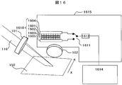
- FIG. 16 is a diagram for explaining the principle of the second embodiment.
- Illumination light 116 emitted from a light source (not shown) is focused on the sample 150 by the lens 101 in one direction (X direction in the case of FIG. 16) and shaped so as to be parallel light in a direction perpendicular thereto. Irradiated from an oblique direction.
- the sample 150 is moved at a constant speed in the X direction by the X stage 304.
- the light directed toward the detection optical system 102 is collected by the detection optical system 102 and disposed on the light receiving surface of the TDI sensor 1610 of the detector 1615.
- the image is formed on the pixel columns 1601, 1602, 1603. Signal detected by the pixel column 1601, 1602, 1603 are input to the A / D converter 1612 in the changeover switch 1611 is outputted from the downstream-side lead-out register 1604 or 1605.
- the output signal from the TDI sensor 1610 converted from an analog signal to a digital signal by the A / D converter 1612 is input to the image processing unit 1614 and processed to detect defects on the sample 150.
- the output signal is equally affected by the AF shift.
- a circuit corresponding to the height deviation information calculation unit 112 of the detector 115 in Example 1 is not required.
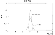
- the profile 1101 of the cross section in the line width direction of the illumination light 116 formed into a linear shape and the reflected / scattered light from the sample 150 illuminated with the illumination light 116 are in a state where there is no AF deviation, the TDI sensor 1610.
- the results of calculating the PSF for each of the pixel columns 1601, 1602, and 1603 when detected in FIG. 6 are displayed as waveforms 1701, 1702, and 1703 superimposed on the profile 1101 of the cross section of the illumination light. Note that the pixel size in the scanning X stage scanning direction of each pixel row 1601, 1602, 1603 of the TDI sensor 1610 was calculated as 0.833 ⁇ m.
- the shift amount of the image detected by the pixel column 1601 and the pixel column 1602 is equal to the shift amount of the image detected by the pixel column 1602 and the pixel column 1603.
- the output from the TDI sensor 1610 can be processed continuously.
- s when a three-stage TDI sensor is used that is, 1 ⁇ 2 of the movement amount of the stage synchronized with the image acquisition for one line of the detection system is expressed by ( ⁇ ) in the stage movement direction. It can be calculated by setting the size p. Even in this case, s becomes a value smaller than 1 ⁇ 2 of the pixel size.
- the amount of movement of the stage synchronized with the image acquisition for one line is equal to the pixel size in the stage moving direction on the sample. As a result, the resolution of the image deteriorates.
- the case where the number of pixel columns of the TDI sensor 1610 is three has been described.
- the number of pixel columns is four or more, the amount of image shift between adjacent pixel columns differs between the central portion and the peripheral portion. Therefore, the output from the TDI sensor 1610 cannot be processed continuously. Therefore, two or three stages are suitable for the TDI sensor 1610.
- FIG. 17B shows a PSF 1704 as a system obtained by shifting and adding the PSF waveforms for the respective pixel columns 1601, 1602, and 1603 of the TDI sensor 1610 by the shift amount obtained based on (Equation 5).
- a graph represented as a profile 1101 is shown. From this result, it can be seen that the PSF of the detection system is improved compared to the illumination light profile.
- FIG. 19 shows the configuration of the image processing unit 1614 of the defect inspection apparatus according to the second embodiment. Although similar to the configuration in the first embodiment described with reference to FIG. 5, there is no input of signals corresponding to the output signals 510A to 510C from the height deviation information calculation unit 112 described with reference to FIG.
- one signal branched from the output 1613A from the first detector 1615A is input to the buffer memory 501A, and as described in FIG. 5 by the first alignment processing unit 511A. Alignment is performed.
- the other branched signal is input to the differentiator 502A, and the signal having detected the pattern of the same shape on the sample 150 previously input to the buffer memory 501A or the pattern of the same region of the adjacent die on the sample 150 is input.
- a difference from the reference signal is calculated (cell comparison or die comparison), and the calculated difference image 1901A is a first threshold signal level set in advance in the temporary defect determination unit 1902A.
- the pseudo defect is removed from the difference image 1901A.
- the signal 1903A from which the pseudo defect signal is removed is input to the AF deviation calculation unit 1904.
- the output 1613B from the second detector 1615B and the output 1613C from the third detector 1615C are similarly processed and compared with the first threshold signal level set in advance in the temporary defect determination units 1902B and 1902C.
- the signals 1903B and 1903C from which the pseudo defect signal has been removed are input to the AF deviation calculation unit 1904.
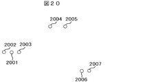
- a method of obtaining the AF deviation amount in the AF deviation calculation unit 1904 will be described with reference to FIG.
- 2001 and 2006 represent the positions of the defect candidates detected by the first detector 1615A
- 2002 and 2004 represent the positions of the defect candidates detected by the second detector 1615B
- 2007 represents the position of the defect candidate detected by the third detector 1615C.
- Relatively defect candidate is in the short distance corresponding relationship assuming the same AF deviation amount is best taken defect candidate (in the case of FIG. 20, 2001 and 2002 and 2003) the AF shift amount from the coordinate information
- the information of the estimated AF deviation amount is used to correct the height deviation of the signals 1903A to 1903C from which the pseudo defect signal has been removed.
- the signals 1905A to 1905C whose height deviation has been corrected by the AF deviation calculation unit 1904 are input to the integration determination unit 1906, integrated into a three-dimensional vector difference image, and a threshold set in advance by the threshold determination unit 1908.
- a defect is extracted in comparison with the value, and the extracted defect information 1909 is output to the overall control unit 301.
- the present embodiment it is possible to perform composition processing after correcting the AF height deviation for an image obtained by imaging from different directions, and to detect a defect with higher sensitivity. At the same time, the classification accuracy of the detected defect can be improved.
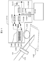
- the configuration of the defect inspection apparatus in FIG. 21 and the present embodiment is basically the same as the configuration shown in FIGS. Only a part of the configuration of the detectors 115A to 115C is different from the configuration and operation described in the first embodiment.
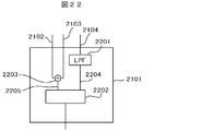
- the two-stage sensor 103 is used as the detector 115, and the shift of the detection position due to the AF shift is calculated by the height shift information calculation unit 112.
- the height deviation information calculation unit 112 evaluates the lightness ratio calculated from the signal output from the A / D converter 109 and the signal output from the A / D converter 110 using the LUT 1506. And calculated the height.
- the AF deviation is calculated using a height deviation information calculation unit 2101 as an alternative to the height deviation information calculation unit 112.
- the two-stage sensor 103 is the same as that described with reference to FIG.
- the switches 2108 and 2109 switch the output from the read-out registers 106 and 107 of the two-stage sensor 103 according to the moving direction of the sample 150.
- the height deviation information calculation unit 2101 includes a signal 2102 output from the A / D converter 2109, a signal 2103 output from the A / D converter 2110, and a signal 2104 that is added and combined by the addition notation 2113. Enter.
- Reference numeral 2201 denotes a low-pass filter that suppresses a high spatial frequency in the stage scanning direction indicated by an arrow in FIG. 21 and outputs a signal 2204 with respect to the signal 2104 added and synthesized in the addition note 2113.
- An adder 2203 adds the signal 2102 output from the A / D converter 2109 and the signal 2103 output from the A / D converter 2110, and outputs a signal 2205. Since the signal 2205 is an image whose resolution is deteriorated in the stage scanning direction with respect to the signal 2104 added and synthesized by the addition notation 2113, the signal 2204 and the signal 2205 are very similar images.
- the pattern matching unit 2202 calculates the shift amount by pattern matching between the signal 2204 and the signal 2205.
- the signal 2205 hardly changes the position of the pattern due to the AF shift, whereas the signal 2204 changes the pattern position due to the AF shift. Therefore, the AF deviation can be calculated by obtaining the deviation amount of the signal 2204 with the signal 2205 as a reference.
- DESCRIPTION OF SYMBOLS 100 ... Inspection optical system 101 ... Lens 102, 102A, 102B, 102D ... Detection optical system 103 ... Two-stage sensor 112 ... Height deviation information calculation part 113 ... Adder 114. Image processing unit 115, 115A, 115B, 115C ... Detector 201 ... Light source unit 202 ... Condensing lens 203 ... Condensing lens 204 ... Photo detector 205 ... Height Detection unit 301 ... Overall control unit 302 ... Stage control means 303 ... Z stage 304 ... X stage 305 ... Y stage 501A, 501B, 501C ...
Landscapes
- Physics & Mathematics (AREA)
- Health & Medical Sciences (AREA)
- Life Sciences & Earth Sciences (AREA)
- Chemical & Material Sciences (AREA)
- Analytical Chemistry (AREA)
- Biochemistry (AREA)
- General Health & Medical Sciences (AREA)
- General Physics & Mathematics (AREA)
- Immunology (AREA)
- Pathology (AREA)
- Engineering & Computer Science (AREA)
- Computer Vision & Pattern Recognition (AREA)
- Signal Processing (AREA)
- Investigating Materials By The Use Of Optical Means Adapted For Particular Applications (AREA)
- Length Measuring Devices By Optical Means (AREA)
Abstract
Description
更に、上記課題を解決するために、本発明では、欠陥検査方法を、試料を載置したステージを一方向に移動させながら試料の表面の法線方向に対して傾斜した方向からステージが移動する一方向に直角な方向に長い線状に成形した光を試料の表面に照射し、この線状に成形した光が照射された試料の表面から第1の方向に反射・散乱した光を集光して複数列の光センサアレイを備えた第1の集光検出手段で検出し、線状に成形した光が照射された試料の表面から第2の方向に反射・散乱した光を集光して複数列の光センサアレイを備えた第2の集光検出手段で検出し、第1の集光検出手段から出力された複数列の光センサアレイからの検出信号を用いて試料の表面に対する第1の集光検出手段の焦点位置のずれを求めると共に第2の集光検出手段から出力された複数列の光センサアレイからの検出信号を用いて試料の表面に対する第2の集光検出手段の焦点位置のずれを求め、この求めた第1の集光検出手段の焦点位置のずれ及び第2の集光検出手段の焦点位置のずれに応じて第1の集光検出手段から出力された検出信号と第2の集光検出手段から出力された検出信号とを補正し、この補正した第1の集光検出手段から出力された検出信号と第2の集光検出手段から出力された検出信号とを統合して試料上の欠陥を検出するようにした。
Xステージ304のX方向への移動と同期して第1の検出器115Aから出力のうち、加算器113から出力された2つの検出素子列104と105との出力を加算した信号509Aは2つに分岐されてその一方が501Aのバッファメモリに入力される。501AはFIFO型のバッファメモリであり、ダイの整数倍ずれた画像を出力する。なお、この中で、複数ダイずれた画像を重ね合わせると、ノイズの低減を図ることができる。511Aは第1の位置あわせ処理部であり、ダイの整数倍ずれた画像間の位置ずれを検出して、分岐した2つの画像の位置ずれがないようにして出力し、差分器502Aに入力する。バッファメモリ501Aに先に入力していた試料150上の同一の形状のパターンを検出した信号または試料150上の隣接するダイの同じ領域のパターンを検出した信号を参照信号として、この参照信号との差分が算出され(セル比較又はダイ比較)、算出された差分画像信号503Aは第2の位置合せ回路部504Aに入力される。また、第1の検出器115Aからの出力のうち、高さずれ情報算出部112からの出力信号510Aも位置合せ回路部504Aに入力されて、別途入力された差分画像信号503Aに対して高さずれ分の補正を行い、欠陥候補の画像が抽出される。
がっており、ステージ走査方向に対して照明系のみでは十分な画像の解像度が得られないことを示している。装置全体での解像度の向上を図るには、検出系の解像度を改善することが有効である。

図11Aには、図9Aに示した構成と同じで、画素を104と105の2つ配置してそれらのサイズを図9Aの場合の半分の1.25μmとした状態を示す。試料150に照射したビームの中心が2つの画素104と105との中間に投影されるように試料150上の照明光の照射領域と検出系の画素の位置が調整されている状態を示している。



α: p/2
ここで、多段のラインセンサを有する検出系の1ライン分の画像取得と同期したステージの移動量を2Sとすると、数3で求められるi(x)がほぼコンスタントの場合には通常の多段のラインセンサ(例えばTDIセンサ(Time Delay Integration sensor:時間遅延積分センサ)で検出する場合と同じくシフト量を画素サイズの1/2にすればよいが、照明光の幅を寄り細く絞ってビームプロファイル1101をより急峻にすると、シフト量は画素のサイズでは決まらず、照明光のビームプロファイルと検出系の解像度で決まり、(数6)のように表される。

本実施例による2段のラインセンサを用いて検出系を採用することにより、解像度が向上していることがわかる。
第2の検出器1615Bからの出力1613B及び第3の検出器1615Cからの出力1613Cも同様に処理されて、仮欠陥判定部1902B及び1902Cにおいて予め設定された第1のしきい値信号レベルと比較されて擬似欠陥信号が除去された信号1903B及び1903CはAFずれ算出部1904に入力される。
Claims (20)
- 試料を載置して少なくとも一方向に移動可能なステージ手段と、
該ステージ手段に載置した前記試料に前記ステージの前記試料を載置する面の法線方向に対して傾斜した方向から線状に成形した光を照射する光照射手段と、
該光照射手段により前記線状に成形した光が照射された前記試料から第1の方向に反射・散乱した光を集光して検出する第1の集光検出手段と、
前記光照射手段により前記線状に成形した光が照射された前記試料から第2の方向に反射・散乱した光を集光して検出する第2の集光検出手段と、
前記第1の集光検出手段から出力された検出信号と前記第2の光検出手段から出力された検出信号とを処理して前記試料状の欠陥を検出する処理手段と、
前記ステージ手段と前記光照射手段と前記第1の光検出手段と前記第2の光検出手段と前記処理手段とを制御する制御手段とを備えた検査装置であって、
前記第1の集光検出手段と前記第2の集光検出手段とはそれぞれ複数列の光センサアレイを備えた光電変換器を有し、
前記処理手段は前記第1の集光検出手段の前記複数列の光センサアレイからの検出信号を用いて前記試料の表面に対する前記第1の集光検出手段の焦点位置のずれを求めると共に前記第2の集光検出手段の前記複数列の光センサアレイからの検出信号を用いて前記試料の表面に対する前記第2の集光検出手段の焦点位置のずれを求め、該求めた前記第1の集光検出手段の焦点位置のずれ及び前記第2の集光検出手段の焦点位置のずれに応じて前記第1の集光検出手段から出力された検出信号と前記第2の集光検出手段から出力された検出信号とを補正し、該補正した前記第1の集光検出手段から出力された検出信号と前記第2の集光検出手段から出力された検出信号とを統合して前記試料上の欠陥を検出することを特徴とする欠陥検査装置。 - 前記集光照射手段により前記線状に成形した光が照射された前記試料から第3の方向に反射・散乱した光を集光して検出する複数列の光センサアレイを備えた光電変換器を有する第3の集光検出手段を更に備えたことを特徴とする請求項1記載の欠陥検査装置。
- 前記第1の集光検出手段と前記第2の集光検出手段とは、それぞれ2列の光センサアレイを有するデュアルラインセンサを光検出器として備えることを特徴とする請求項1記載の欠陥検査装置。
- 前記第1の集光検出手段と前記第2の集光検出手段とはそれぞれ前記試料上に形成された繰り返しパターンにより発生する回折光パターンを遮光する空間フィルタを備え、該空間フィルタを透過した光を検出することを特徴とする請求項1記載の欠陥検査装置。
- 前記試料表面の高さを光学的に検出する高さ検出手段をされに備えることを特徴とする請求項1記載の欠陥検査装置。
- 試料を載置して少なくとも一方向に移動可能なステージ手段と、
該ステージ手段に載置した前記試料に前記ステージの前記試料を載置する面の法線方向に対して傾斜した方向から線状に成形した光を照射する光照射手段と、
該光照射手段により前記線状に成形した光が照射された前記試料から第1の方向に反射・散乱した光を集光して検出する第1の集光検出手段と、
前記光照射手段により前記線状に成形した光が照射された前記試料から第2の方向に反射・散乱した光を集光して検出する第2の集光検出手段と、
前記第1の集光検出手段から出力された検出信号と前記第2の光検出手段から出力された検出信号とを処理して前記試料状の欠陥を検出する処理手段と、
前記ステージ手段と前記光照射手段と前記第1の光検出手段と前記第2の光検出手段と前記処理手段とを制御する制御手段とを備えた 検査装置であって、
前記第1の集光検出手段と前記第2の集光検出手段とはそれぞれ複数列の光センサアレイを備えた光電変換器を有し、
前記制御手段は前記ステージ手段を制御して該ステージ手段を前記一方向に連続的に移動させると共に前記第1の集光検出手段の光電変換器と前記第2の集光検出手段の光電変換器とを制御して前記光照射手段により線状に成形した光が照射された前記試料からの反射散乱光を前記ステージ手段の移動と同期させて検出し、
前記制御手段は更に前記処理手段を制御して前記第1の集光検出手段の光電変換器と前記第2の集光検出手段の光電変換器とから出力された検出信号を前記ステージ手段の移動との前記動機とは異なるタイミングで処理し、該同期とは異なるタイミングで処理した前記前記第1の集光検出手段の光電変換器と前記第2の集光検出手段の光電変換器とから出力された検出信号を統合して前記試料状の欠陥を検出する
ことを特徴とする欠陥検査装置。 - 前記集光照射手段により前記線状に成形した光が照射された前記試料から第3の方向に反射・散乱した光を集光して検出する複数列の光センサアレイを備えた光電変換器を有する第3の集光検出手段を更に備えたことを特徴とする請求項6記載の欠陥検査装置。
- 前記第1の集光検出手段と前記第2の集光検出手段とは、それぞれ2列の光センサアレイを有するデュアルラインセンサを光検出器として備えることを特徴とする請求項6記載の欠陥検査装置。
- 前記第1の集光検出手段と前記第2の集光検出手段とはそれぞれ前記試料上に形成された繰り返しパターンにより発生する回折光パターンを遮光する空間フィルタを備え、該空間フィルタを透過した光を検出することを特徴とする請求項6記載の欠陥検査装置。
- 前記試料表面の高さを光学的に検出する高さ検出手段をされに備えることを特徴とする請求項6記載の欠陥検査装置。
- 試料を載置したステージを一方向に移動させながら前記試料の表面の法線方向に対して傾斜した方向から前記ステージが移動する前記一方向に直角な方向に長い線状に成形した光を前記試料の表面に照射し、
該線状に成形した光が照射された前記試料の表面から第1の方向に反射・散乱した光を集光して複数列の光センサアレイを備えた第1の集光検出手段で検出し、
前記線状に成形した光が照射された前記試料の表面から第2の方向に反射・散乱した光を集光して複数列の光センサアレイを備えた第2の集光検出手段で検出し、
前記第1の集光検出手段から出力された前記複数列の光センサアレイからの検出信号を用いて前記試料の表面に対する前記第1の集光検出手段の焦点位置のずれを求めると共に前記第2の集光検出手段から出力された前記複数列の光センサアレイからの検出信号を用いて前記試料の表面に対する前記第2の集光検出手段の焦点位置のずれを求め、
該求めた前記第1の集光検出手段の焦点位置のずれ及び前記第2の集光検出手段の焦点位置のずれに応じて前記第1の集光検出手段から出力された検出信号と前記第2の集光検出手段から出力された検出信号とを補正し、
該補正した前記第1の集光検出手段から出力された検出信号と前記第2の集光検出手段から出力された検出信号とを統合して前記試料上の欠陥を検出する
ことを特徴とする欠陥検査方法。 - 前記線状に成形した光が照射された前記試料の表面から第3の方向に反射・散乱した光を集光して複数列の光センサアレイを備えた第3の集光検出手段で検出し、
前記第3の集光検出手段から出力された前記複数列の光センサアレイからの検出信号を用いて前記試料の表面に対する前記第3の集光検出手段の焦点位置のずれを求め、該求めた前記第3の集光検出手段の焦点位置のずれに応じて前記第3の集光検出手段から出力された検出信号を補正し、該補正した前記第3の集光検出手段から出力された検出信号と前記補正した前記第1の集光検出手段から出力された検出信号と前記第2の集光検出手段から出力された検出信号とを統合して前記試料状の欠陥を検出することを特徴とする請求項11記載の欠陥検査方法。 - 前記第1の集光検出手段で集光した前記試料の表面から第1の方向に反射・散乱した光を前記第1の集光検出手段の2列の光センサアレイで検出し、該2列の光センサアレイの各列からの検出信号を用いて前記試料の表面に対する前記第1の集光検出手段の焦点位置のずれを求め、前記第2の集光検出手段で集光した前記試料の表面から第2の方向に反射・散乱した光を前記第2の集光検出手段の2列の光センサアレイで検出し、該2列の光センサアレイの各列からの検出信号を用いて前記試料の表面に対する前記第2の集光検出手段の焦点位置のずれを求めることを特徴とする請求項11記載の欠陥検査方法。
- 前記第1の集光検出手段と前記第2の集光検出手段とは、それぞれ前記試料上に形成された繰り返しパターンにより発生する回折光パターンを遮光した光を検出することを特徴とする請求項11記載の欠陥検査方法。
- 前記試料を載置したステージを一方向に移動させながら前記線状に成形した光を前記試料の表面に照射しているときに、前記試料表面の高さを光学的に検出し、該検出した高さ情報に基づいて前記ステージを上下させて前記試料表面の高さを制御することを特徴とする請求項11記載の欠陥検査方法。
- 試料を載置したステージを一方向に移動させながら前記試料の表面の法線方向に対して傾斜した方向から前記ステージが移動する前記一方向に直角な方向に長い線状に成形した光を前記試料の表面に照射し、
該線状に成形した光が照射された前記試料の表面から第1の方向に反射・散乱した光を集光して複数列の光センサアレイを有する光電変換器を備えた第1の集光検出手段で前記ステージの前記一方向への移動と同期して検出し、
前記線状に成形した光が照射された前記試料の表面から第2の方向に反射・散乱した光を集光して複数列の光センサアレイを有する光電変換器を備えた第2の集光検出手段で前記ステージの前記一方向への移動と同期して検出し、
前記第1の集光検出手段の光電変換器と前記第2の集光検出手段の光電変換器とから出力された検出信号を前記ステージの移動との前記同期とは異なるタイミングで処理し、該同期とは異なるタイミングで処理した前記前記第1の集光検出手段の光電変換器と前記第2の集光検出手段の光電変換器とから出力された検出信号を統合して前記試料上の欠陥を検出することを特徴とする欠陥検査方法。 - 前記第1の集光検出手段と前記第2の集光検出手段とは、それぞれ前記試料上に形成された繰り返しパターンにより発生する回折光パターンを遮光した光を検出することを特徴とする請求項16記載の欠陥検査方法。
- 前記試料を載置したステージを一方向に移動させながら前記線状に成形した光を前記試料の表面に照射しているときに、前記試料表面の高さを光学的に検出し、該検出した高さ情報に基づいて前記ステージを上下させて前記試料表面の高さを制御することを特徴とする請求項16記載の欠陥検査方法。
- 試料を載置して少なくとも一方向に移動可能なステージ手段と、
該ステージ手段に載置した前記試料に前記ステージの前記試料を載置する面の法線方向に対して傾斜した方向から線状に成形した光を照射する光照射手段と、
該光照射手段により前記線状に成形した光が照射された前記試料から反射・散乱した光を集光して検出する集光検出手段と、
前記集光検出手段から出力された検出信号を処理して前記試料状の欠陥を検出する処理手段と、
前記ステージ手段と前記光照射手段と前記光検出手段と前記処理手段とを制御する制御手段を備えた検査装置であって、
前記集光検出手段は、前記ステージの移動方向の前記試料面上での共役な大きさが前記光照射手段が前記試料上に線上に照明する照明光の線幅に対して小さい光電変換面を有する複数列の光センサアレイを備えた光電変換器を有し、
前記複数列の光センサアレイで検出した、一定の時間差をもって検出した電気信号を加算する信号加算手段を有し、
前記制御手段は前記ステージ手段が前記一定の時間差の区間に移動量が前記光電変換面の前記試料上での対応する大きさ以下になるように制御することを特徴とする欠陥検査装置。 - 試料を載置したステージを一方向に移動させながら前記試料の表面の法線方向に対して傾斜した方向から前記ステージが移動する前記一方向に直角な方向に長い線状に成形した光を前記試料の表面に照射し、
該線状に成形した光が照射された前記試料の表面から反射・散乱した光を集光して複数列の光センサアレイを有する光電変換器を備えた集光検出手段で前記ステージの前記一方向への移動と同期して検出し、
前記複数列の光センサアレイの電気信号を、異なる時間で検出した電気信号をもって加算する欠陥検出方法であって、
前記ステージの移動量は前記試料上における前記光電変換器の光電変換面のステージ移動方向の大きさに以下になるように制御することを特徴とする欠陥検査方法。
Priority Applications (2)
| Application Number | Priority Date | Filing Date | Title |
|---|---|---|---|
| KR1020137015141A KR101553126B1 (ko) | 2010-12-13 | 2011-11-08 | 결함 검사 방법 및 그 장치 |
| US13/993,888 US9239283B2 (en) | 2010-12-13 | 2011-11-08 | Defect inspection method and device therefor |
Applications Claiming Priority (2)
| Application Number | Priority Date | Filing Date | Title |
|---|---|---|---|
| JP2010-276914 | 2010-12-13 | ||
| JP2010276914A JP2012127682A (ja) | 2010-12-13 | 2010-12-13 | 欠陥検査方法及びその装置 |
Publications (1)
| Publication Number | Publication Date |
|---|---|
| WO2012081338A1 true WO2012081338A1 (ja) | 2012-06-21 |
Family
ID=46244451
Family Applications (1)
| Application Number | Title | Priority Date | Filing Date |
|---|---|---|---|
| PCT/JP2011/075758 Ceased WO2012081338A1 (ja) | 2010-12-13 | 2011-11-08 | 欠陥検査方法及びその装置 |
Country Status (4)
| Country | Link |
|---|---|
| US (1) | US9239283B2 (ja) |
| JP (1) | JP2012127682A (ja) |
| KR (1) | KR101553126B1 (ja) |
| WO (1) | WO2012081338A1 (ja) |
Cited By (1)
| Publication number | Priority date | Publication date | Assignee | Title |
|---|---|---|---|---|
| CN118410088A (zh) * | 2024-05-08 | 2024-07-30 | 济南作为科技有限公司 | 数据处理方法、装置、设备、存储介质及计算机程序产品 |
Families Citing this family (15)
| Publication number | Priority date | Publication date | Assignee | Title |
|---|---|---|---|---|
| JP5684028B2 (ja) * | 2011-03-31 | 2015-03-11 | Hoya株式会社 | 転写用マスクの製造方法および半導体デバイスの製造方法 |
| JP5997039B2 (ja) * | 2012-12-26 | 2016-09-21 | 株式会社日立ハイテクノロジーズ | 欠陥検査方法および欠陥検査装置 |
| JP6738730B2 (ja) * | 2013-10-24 | 2020-08-12 | シグニファイ ホールディング ビー ヴィSignify Holding B.V. | 欠陥検査システム及び方法 |
| KR102399493B1 (ko) | 2014-01-23 | 2022-05-19 | 삼성전자주식회사 | 반도체 칩 표면검사 장치 및 이를 이용한 반도체 칩의 표면검사 방법 |
| KR102493466B1 (ko) | 2015-10-14 | 2023-01-30 | 삼성전자 주식회사 | 자동 초점 조정 장치 및 반도체 소자의 제조 방법 |
| JP6358351B1 (ja) * | 2017-03-21 | 2018-07-18 | Jfeスチール株式会社 | 表面欠陥検査方法及び表面欠陥検査装置 |
| US11143600B2 (en) * | 2018-02-16 | 2021-10-12 | Hitachi High-Tech Corporation | Defect inspection device |
| US10859453B2 (en) | 2018-11-28 | 2020-12-08 | International Business Machines Corporation | Mechanical integrity sensor |
| KR102250085B1 (ko) | 2019-08-13 | 2021-05-10 | (주)케파 | 광학 검사 장치 |
| US11442021B2 (en) | 2019-10-11 | 2022-09-13 | Kla Corporation | Broadband light interferometry for focal-map generation in photomask inspection |
| JP7365510B2 (ja) * | 2020-01-29 | 2023-10-19 | エーエスエムエル ネザーランズ ビー.ブイ. | 基板上の周期構造を測定するための計測方法およびデバイス |
| TW202142863A (zh) * | 2020-04-10 | 2021-11-16 | 荷蘭商Asml荷蘭公司 | 處理用於晶圓檢測之參考資料 |
| JP7392582B2 (ja) * | 2020-06-12 | 2023-12-06 | オムロン株式会社 | 検査システムおよび検査方法 |
| US12360058B2 (en) | 2020-12-21 | 2025-07-15 | Kla Corporation | Integration of an optical height sensor in mask inspection tools |
| CN114379830B (zh) * | 2022-03-23 | 2022-06-10 | 南京伟测半导体科技有限公司 | 一种晶舟盒内晶圆位置检测装置 |
Citations (5)
| Publication number | Priority date | Publication date | Assignee | Title |
|---|---|---|---|---|
| JP2005221368A (ja) * | 2004-02-05 | 2005-08-18 | Olympus Corp | 観察装置及びその観察方法 |
| JP2006515668A (ja) * | 2002-09-30 | 2006-06-01 | アプライド マテリアルズ イスラエル リミテッド | 光学的検査のための照明システム |
| JP2009010325A (ja) * | 2007-05-31 | 2009-01-15 | Hitachi High-Technologies Corp | 検査装置及び検査方法 |
| JP2009180691A (ja) * | 2008-02-01 | 2009-08-13 | Hitachi High-Technologies Corp | 欠陥検査方法及び欠陥検査装置 |
| JP2010256340A (ja) * | 2009-03-31 | 2010-11-11 | Hitachi High-Technologies Corp | 高速検査方法とその装置 |
Family Cites Families (7)
| Publication number | Priority date | Publication date | Assignee | Title |
|---|---|---|---|---|
| US5463459A (en) | 1991-04-02 | 1995-10-31 | Hitachi, Ltd. | Method and apparatus for analyzing the state of generation of foreign particles in semiconductor fabrication process |
| US6608676B1 (en) | 1997-08-01 | 2003-08-19 | Kla-Tencor Corporation | System for detecting anomalies and/or features of a surface |
| JP3566589B2 (ja) | 1998-07-28 | 2004-09-15 | 株式会社日立製作所 | 欠陥検査装置およびその方法 |
| JP4654408B2 (ja) * | 2004-06-22 | 2011-03-23 | レーザーテック株式会社 | 検査装置、検査方法及びパターン基板の製造方法 |
| JP2009053132A (ja) * | 2007-08-29 | 2009-03-12 | Hitachi High-Technologies Corp | 欠陥検査方法および欠陥検査装置 |
| JP2009156574A (ja) * | 2007-12-25 | 2009-07-16 | Hitachi High-Technologies Corp | 検査装置及び検査方法 |
| JP2010190722A (ja) | 2009-02-18 | 2010-09-02 | Hitachi High-Technologies Corp | 欠陥検査方法及び欠陥検査装置 |
-
2010
- 2010-12-13 JP JP2010276914A patent/JP2012127682A/ja active Pending
-
2011
- 2011-11-08 WO PCT/JP2011/075758 patent/WO2012081338A1/ja not_active Ceased
- 2011-11-08 KR KR1020137015141A patent/KR101553126B1/ko not_active Expired - Fee Related
- 2011-11-08 US US13/993,888 patent/US9239283B2/en active Active
Patent Citations (5)
| Publication number | Priority date | Publication date | Assignee | Title |
|---|---|---|---|---|
| JP2006515668A (ja) * | 2002-09-30 | 2006-06-01 | アプライド マテリアルズ イスラエル リミテッド | 光学的検査のための照明システム |
| JP2005221368A (ja) * | 2004-02-05 | 2005-08-18 | Olympus Corp | 観察装置及びその観察方法 |
| JP2009010325A (ja) * | 2007-05-31 | 2009-01-15 | Hitachi High-Technologies Corp | 検査装置及び検査方法 |
| JP2009180691A (ja) * | 2008-02-01 | 2009-08-13 | Hitachi High-Technologies Corp | 欠陥検査方法及び欠陥検査装置 |
| JP2010256340A (ja) * | 2009-03-31 | 2010-11-11 | Hitachi High-Technologies Corp | 高速検査方法とその装置 |
Cited By (1)
| Publication number | Priority date | Publication date | Assignee | Title |
|---|---|---|---|---|
| CN118410088A (zh) * | 2024-05-08 | 2024-07-30 | 济南作为科技有限公司 | 数据处理方法、装置、设备、存储介质及计算机程序产品 |
Also Published As
| Publication number | Publication date |
|---|---|
| JP2012127682A (ja) | 2012-07-05 |
| US20130293879A1 (en) | 2013-11-07 |
| US9239283B2 (en) | 2016-01-19 |
| KR101553126B1 (ko) | 2015-09-14 |
| KR20130086370A (ko) | 2013-08-01 |
Similar Documents
| Publication | Publication Date | Title |
|---|---|---|
| KR101553126B1 (ko) | 결함 검사 방법 및 그 장치 | |
| US7227984B2 (en) | Method and apparatus for identifying defects in a substrate surface by using dithering to reconstruct under-sampled images | |
| US20130294677A1 (en) | Defect inspection method and defect inspection device | |
| KR102326402B1 (ko) | 포커스 용적 측정 방법을 이용한 웨이퍼 검사 | |
| US8427634B2 (en) | Defect inspection method and apparatus | |
| US7619203B2 (en) | High throughput multi beam detection system and method | |
| JP5320187B2 (ja) | 欠陥検査方法及び欠陥検査装置 | |
| US7248732B2 (en) | Pattern inspection method and inspection apparatus | |
| US8416292B2 (en) | Defect inspection apparatus and method | |
| US20040036864A1 (en) | System for detecting anomalies and/or features of a surface | |
| US20040240723A1 (en) | Pattern inspection method and its apparatus | |
| WO2018216277A1 (ja) | 欠陥検査装置及び欠陥検査方法 | |
| JP2010025713A (ja) | 欠陥検査方法及び欠陥検査装置 | |
| JP2008275540A (ja) | パターン欠陥検査装置および方法 | |
| KR20160037192A (ko) | 다이별 검사를 위한 오토포커스 시스템 및 방법 | |
| US12345661B2 (en) | Defect inspection apparatus and defect inspection method | |
| JP2012117814A (ja) | 欠陥検査装置および欠陥検査方法 | |
| US12366538B2 (en) | Defect inspection apparatus and defect inspection method | |
| WO2010113228A1 (ja) | 検査装置及び検査方法 | |
| JP5593209B2 (ja) | 検査装置 | |
| KR20230061424A (ko) | 3차원 웨이퍼 구조체들에 대한 비닝 향상된 결함 검출 방법 | |
| US20260049945A1 (en) | Pattern inspection apparatus and pattern inspection method |
Legal Events
| Date | Code | Title | Description |
|---|---|---|---|
| 121 | Ep: the epo has been informed by wipo that ep was designated in this application |
Ref document number: 11848830 Country of ref document: EP Kind code of ref document: A1 |
|
| ENP | Entry into the national phase |
Ref document number: 20137015141 Country of ref document: KR Kind code of ref document: A |
|
| NENP | Non-entry into the national phase |
Ref country code: DE |
|
| WWE | Wipo information: entry into national phase |
Ref document number: 13993888 Country of ref document: US |
|
| 122 | Ep: pct application non-entry in european phase |
Ref document number: 11848830 Country of ref document: EP Kind code of ref document: A1 |