WO2012057514A2 - 인터커넥션 부분이 분리 설치된 염료감응 태양전지의 모노리식 모듈구조 - Google Patents
인터커넥션 부분이 분리 설치된 염료감응 태양전지의 모노리식 모듈구조 Download PDFInfo
- Publication number
- WO2012057514A2 WO2012057514A2 PCT/KR2011/008013 KR2011008013W WO2012057514A2 WO 2012057514 A2 WO2012057514 A2 WO 2012057514A2 KR 2011008013 W KR2011008013 W KR 2011008013W WO 2012057514 A2 WO2012057514 A2 WO 2012057514A2
- Authority
- WO
- WIPO (PCT)
- Prior art keywords
- layer
- dye
- electrode layer
- cell
- solar cell
- Prior art date
- Legal status (The legal status is an assumption and is not a legal conclusion. Google has not performed a legal analysis and makes no representation as to the accuracy of the status listed.)
- Ceased
Links
Images

Classifications
-
- H—ELECTRICITY
- H10—SEMICONDUCTOR DEVICES; ELECTRIC SOLID-STATE DEVICES NOT OTHERWISE PROVIDED FOR
- H10F—INORGANIC SEMICONDUCTOR DEVICES SENSITIVE TO INFRARED RADIATION, LIGHT, ELECTROMAGNETIC RADIATION OF SHORTER WAVELENGTH OR CORPUSCULAR RADIATION
- H10F19/00—Integrated devices, or assemblies of multiple devices, comprising at least one photovoltaic cell covered by group H10F10/00, e.g. photovoltaic modules
- H10F19/90—Structures for connecting between photovoltaic cells, e.g. interconnections or insulating spacers
-
- H—ELECTRICITY
- H01—ELECTRIC ELEMENTS
- H01G—CAPACITORS; CAPACITORS, RECTIFIERS, DETECTORS, SWITCHING DEVICES, LIGHT-SENSITIVE OR TEMPERATURE-SENSITIVE DEVICES OF THE ELECTROLYTIC TYPE
- H01G9/00—Electrolytic capacitors, rectifiers, detectors, switching devices, light-sensitive or temperature-sensitive devices; Processes of their manufacture
- H01G9/20—Light-sensitive devices
- H01G9/2068—Panels or arrays of photoelectrochemical cells, e.g. photovoltaic modules based on photoelectrochemical cells
-
- H—ELECTRICITY
- H01—ELECTRIC ELEMENTS
- H01G—CAPACITORS; CAPACITORS, RECTIFIERS, DETECTORS, SWITCHING DEVICES, LIGHT-SENSITIVE OR TEMPERATURE-SENSITIVE DEVICES OF THE ELECTROLYTIC TYPE
- H01G9/00—Electrolytic capacitors, rectifiers, detectors, switching devices, light-sensitive or temperature-sensitive devices; Processes of their manufacture
- H01G9/20—Light-sensitive devices
- H01G9/2068—Panels or arrays of photoelectrochemical cells, e.g. photovoltaic modules based on photoelectrochemical cells
- H01G9/2081—Serial interconnection of cells
-
- H—ELECTRICITY
- H01—ELECTRIC ELEMENTS
- H01G—CAPACITORS; CAPACITORS, RECTIFIERS, DETECTORS, SWITCHING DEVICES, LIGHT-SENSITIVE OR TEMPERATURE-SENSITIVE DEVICES OF THE ELECTROLYTIC TYPE
- H01G9/00—Electrolytic capacitors, rectifiers, detectors, switching devices, light-sensitive or temperature-sensitive devices; Processes of their manufacture
- H01G9/20—Light-sensitive devices
- H01G9/2027—Light-sensitive devices comprising an oxide semiconductor electrode
- H01G9/2031—Light-sensitive devices comprising an oxide semiconductor electrode comprising titanium oxide, e.g. TiO2
-
- H—ELECTRICITY
- H01—ELECTRIC ELEMENTS
- H01G—CAPACITORS; CAPACITORS, RECTIFIERS, DETECTORS, SWITCHING DEVICES, LIGHT-SENSITIVE OR TEMPERATURE-SENSITIVE DEVICES OF THE ELECTROLYTIC TYPE
- H01G9/00—Electrolytic capacitors, rectifiers, detectors, switching devices, light-sensitive or temperature-sensitive devices; Processes of their manufacture
- H01G9/20—Light-sensitive devices
- H01G9/2059—Light-sensitive devices comprising an organic dye as the active light absorbing material, e.g. adsorbed on an electrode or dissolved in solution
-
- Y—GENERAL TAGGING OF NEW TECHNOLOGICAL DEVELOPMENTS; GENERAL TAGGING OF CROSS-SECTIONAL TECHNOLOGIES SPANNING OVER SEVERAL SECTIONS OF THE IPC; TECHNICAL SUBJECTS COVERED BY FORMER USPC CROSS-REFERENCE ART COLLECTIONS [XRACs] AND DIGESTS
- Y02—TECHNOLOGIES OR APPLICATIONS FOR MITIGATION OR ADAPTATION AGAINST CLIMATE CHANGE
- Y02E—REDUCTION OF GREENHOUSE GAS [GHG] EMISSIONS, RELATED TO ENERGY GENERATION, TRANSMISSION OR DISTRIBUTION
- Y02E10/00—Energy generation through renewable energy sources
- Y02E10/50—Photovoltaic [PV] energy
- Y02E10/542—Dye sensitized solar cells
-
- Y—GENERAL TAGGING OF NEW TECHNOLOGICAL DEVELOPMENTS; GENERAL TAGGING OF CROSS-SECTIONAL TECHNOLOGIES SPANNING OVER SEVERAL SECTIONS OF THE IPC; TECHNICAL SUBJECTS COVERED BY FORMER USPC CROSS-REFERENCE ART COLLECTIONS [XRACs] AND DIGESTS
- Y02—TECHNOLOGIES OR APPLICATIONS FOR MITIGATION OR ADAPTATION AGAINST CLIMATE CHANGE
- Y02P—CLIMATE CHANGE MITIGATION TECHNOLOGIES IN THE PRODUCTION OR PROCESSING OF GOODS
- Y02P70/00—Climate change mitigation technologies in the production process for final industrial or consumer products
- Y02P70/50—Manufacturing or production processes characterised by the final manufactured product
Definitions
- the present invention relates to a monolithic structure of a dye-sensitized solar cell, and relates to a cell connection structure of a monolithic module provided such that an interconnection electrode portion of a solar cell is separated from a photoelectric conversion layer of a neighboring solar cell.
- a technology for improving photoelectric conversion efficiency by connecting a plurality of solar cells has been developed. According to the composition of the cells constituting the dye-sensitized solar cell module and the method of connecting the cells, it is classified into W type, Z type, Monolithic type and current collecting grid type.
- W-type module is a cell-to-cell series configuration.
- the first electrode of the cell and the second electrode of the adjacent cell use the same electrode and are formed in pairs, so that there is no need for interconnection wiring connecting the separate cells.
- half of the cells have a disadvantage in that the absorption of light due to the electrolyte is large because light passes through the electrolyte and reaches the photoelectrode.
- the Z type connects the interconnection wiring through the partition walls between the unit cells. Due to the sealing work between the unit cells and the interconnection wiring for connecting the first electrode of the cell and the second electrode of the neighboring cell in series, the device fabrication process is complicated and the effective area is reduced.
- the module is a parallel cell-to-cell module that forms a metal grid wiring for collecting current on the conductive substrate surface and drawing it out without dividing the unit cells.
- the structure of a large number of dye-sensitized solar cells in one large cell sealed in the form of a large-capacity method is the simplest device structure, which has the advantage of good productivity. If the area is increased, the dead space is rapidly increased and the efficiency is reduced.
- Monolithic module structure is Z-type power generation type, and it has the advantage of using only one transparent conductive substrate and all processes can be inline process, so that the module structure with high productivity by connecting multiple cells of dye-sensitized solar cell
- a problem has been pointed out in the configuration of connecting cells that the first electrode of the first cell and the first electrode of the neighboring cell are easily connected.
- the first electrode layer is formed on the transparent substrate, the photoelectric conversion layer is formed on the first electrode layer, and the photoelectric conversion layer is a photoelectrode layer to which dye is adsorbed, an electrolyte layer and an insulating layer are formed on the photoelectrode layer. And a catalyst layer on the insulating layer, followed by the second electrode layer.
- the second electrode layer of the first cell is in electrical contact with the first electrode layer of a neighboring cell with an insulating partition interposed therebetween.
- TCO first electrode layer
- the lower portion of the insulating partition wall for electrical insulation with neighboring solar cells is formed on the transparent substrate away from the first electrode layer (TCO) of the neighboring cell, and at the same time a portion of the lower portion of the insulating partition wall neighbors
- the structure covering the first electrode layer of the battery cell effectively prevents a short circuit between the first electrode of the photoelectric conversion layer and the neighboring first electrode layer TCO so that the first electrode layer of the neighboring cell does not become a short circuit. And close the interconnection between and neighboring cells. It also provides a method that can be easily manufactured by screen printing printing while allowing the interconnection to closely adhere to the insulating partition wall.
- the present invention relates to a structure of a monolithic dye-sensitized solar cell module and is configured by electrically connecting a plurality of solar cell.
- the plurality of solar cells of the present invention can be determined by designing an appropriate number according to the use of the monolithic dye-sensitized solar cell.
- a plurality of unit solar cells formed of a photoelectric conversion layer and a second electrode layer composed of a first electrode layer, a photoelectrode layer, an electrolyte layer, an insulating layer, and a catalyst layer are formed on a transparent substrate.
- an insulating partition wall is formed between the cells, and in order to connect the second electrode layer of each unit cell and the first electrode layer of the neighboring unit cell, an insulating partition wall is formed between the cells and insulated.
- the present invention has a structure in which a plurality of dye-sensitized solar cells are connected in a structure in which the second electrode layer of the first dye-sensitized solar cell is in contact with the first electrode layer of a neighboring second dye-sensitized solar cell.
- an interconnection is provided as a structure for connecting a second electrode layer of the first dye-sensitized solar cell and a first electrode layer of a neighboring second dye-sensitized solar cell. It is done.
- the present invention is a step of forming a pattern and the first electrode layer on the portion forming the insulating partition on the transparent substrate (a), the step of forming an insulating partition on the portion where the pattern is formed (b), one side lower end of the insulating partition (C) forming a photoelectric conversion layer and a second electrode layer comprising a photoelectrode layer, an electrolyte layer, an insulating layer, and a catalyst layer on the one electrode layer, with the second electrode layer and the insulating partition wall of one dye-sensitized solar cell interposed therebetween.
- step (D) forming an interconnection electrically connecting the first electrode layer of the neighboring dye-sensitized solar cell while crossing the insulating partition wall, and forming a V-shape between one dye-sensitized solar cell and the encapsulant or interconnection.
- the transparent substrate of the present invention uses a transparent conductive film for display and a transparent conductive film for solar cells, and is generally manufactured by coating a conductive material on glass (bare glass, soda-lime) which is an electrical insulator.
- the glass is an electrical insulator and has an electrical conductivity of 10 -10 to 10 -11 ( ⁇ cm) -1 at room temperature.
- Various TCOs are applied to the surface of the glass in order to impart electrical conductivity to the glass, which is insulator. (Transparent Conductive Oxide Film) or metal is coated with a transparent conductive coating, and transparent conductive coating is produced by this.
- the transparent conductive oxide film (TCO) is electrically insulated from the first dye-sensitized solar cell and the portion of the partition wall between the neighboring second dye-sensitized solar cell.
- the insulating partition portion is formed on the transparent substrate to be separated from the first electrode layer (TCO), and at the same time, the lower end portion of the insulating partition structure covers the first electrode layer (TCO) of the neighboring solar cell to form a structure of the photoelectric conversion layer of the cell.
- the first electrode layer TCO of the cell adjacent to the photoelectrode is configured to not short-circuit.
- the transparent conductive film of the conductive glass of the present invention is a method of forming a pattern on a portion where a partition wall is installed to expose an image formed on a mask using PR to develop a PR, and then etching the pattern using an etchant.
- Forming method in case of using FTO, because FTO has excellent chemical resistance and chemical etching using etchant is impossible, it is possible to use pattern forming method using laser, and transparent conductive oxide film is formed on the upper surface of glass substrate.
- a photoresist pattern is formed on a portion not to be formed, a transparent conductive oxide film is formed on the upper surface of the glass substrate, and then the photoresist on the glass substrate is removed.
- a partition wall which is an insulating layer between cells, is first provided in a portion where a pattern on a transparent glass substrate is formed.
- the lower part of the insulating partition for electrical insulation with neighboring cells is formed on the transparent substrate so as to be separated from the first electrode layer (TCO) of the cell, and the lower part of the insulating partition is formed of the first electrode layer (TCO) of the neighboring cell.
- Forming a covering structure prevents a short circuit between the photoelectrode and the neighboring TCO, thereby effectively preventing a short circuit between the first electrode layer TCO of the neighboring cell.
- the insulating barrier between the cells has a function of inhibiting the movement of the redox material in the electrolyte layer, and the insulating barrier is the first of the second dye-sensitized solar cell adjacent to the first electrode layer of the first dye-sensitized solar cell. Short circuit with the electrode layer is prevented from occurring. Therefore, it is preferable that the photoelectric conversion elements are partitioned by the inter-cell insulating partition, and the film is so dense that the redox material of the electrolyte layer cannot pass through the inter-cell insulating partition by the insulating partition.
- the dense membrane may be a membrane through which redox materials cannot pass between adjacent cells, and examples thereof include porous bodies of independent bubbles.
- the insulating resin film material include silicon oxide, fluorine oxide, zinc oxide, lead oxide, bismuth oxide, titanium oxide, aluminum oxide, magnesium oxide and the like.
- the method of forming the insulating partition walls between cells includes a paste containing semiconductor particles on a substrate such as a screen printing method or an inkjet method on a pattern portion formed between the first and second dye-sensitized solar cells. The method of apply
- Interconnection wirings are formed and provided outside the inter-cell insulating partition on the part where the cell pattern is formed on the transparent glass substrate.
- the interconnection line of the present invention is connected to make an electrical connection between the second electrode layer provided on the upper portion of the first dye-sensitized solar cell and the first electrode layer provided on the lower portion of the neighboring second dye-sensitized solar cell.
- the electrical connection by the interconnection wiring is connected along one outer side of the insulating layer partition, that is, along one outer side of the partition not contacting the first electrode layer of the first dye-sensitized solar cell.
- the interconnect wiring may use a film in which conductive particles are dispersed.
- the film in which the conductive particles applied to the interconnection of the present invention is dispersed may be preferably an anisotropic conductive film, and the conductive particles may be coated with metal powder particles, conductive polymer particles, or insulating resin particles.
- the film may further include a space particle having a size smaller than or equal to that of the conductive particle, thereby enhancing elasticity of the interconnection and adhesion to the insulating layer partition wall.
- the spacer particle may be a rubber component having elasticity, and preferably a rubber component of butadiene can be used.
- a photoelectric conversion layer composed of an electrolyte layer and an insulating layer catalyst layer is formed.
- the photoelectrode layer of the first dye-sensitized solar cell of the present invention can be used as one or two or more kinds of semiconductors such as titanium oxide and zinc oxide, which are known as porous semiconductor layers. Titanium oxide can be used.
- the semiconductor layer may be formed in various forms such as in a particle state or in a film state.
- a method of forming a porous semiconductor layer on a substrate a semiconductor on a substrate such as a screen printing method or an ink jet method may be used. A paste containing particles is applied and then fired.
- the surface area of the porous semiconductor layer is large, but in the present invention, two or more kinds of dyes are included to absorb sunlight having a broad wavelength.
- the size of the porous semiconductor particles is arranged in a small, large and small order from the light-receiving surface.
- the semiconductor particles of the present invention have an average particle diameter of 1 nm to 500 nm and a surface area of about 10 to 200 m 2 / g is preferable.
- Drying and firing of the porous semiconductor layer of the present invention is dried and fired in a general air atmosphere in the range of 50 to 800 ° C. for about 10 seconds to 4 hours, and this drying and firing is performed once or at a single temperature with a single temperature. It can be performed twice or more.
- the dye of the first dye-sensitized solar cell of the present invention is adsorbed on the porous semiconductor layer to perform the function of photoelectric conversion.
- the porous semiconductor layer of the present invention forms a multi-layered structure in the order of the small particle porous semiconductor, the large particle porous semiconductor, the small particle porous semiconductor from the light-receiving surface in order to use the incident light to the maximum, and the organic pigment according to each particle size , Metal complex dyes are selected and adsorbed.
- Ru-based dyes Longjin Semichem Publication No. 10-2008-77765
- the dyes used in the present invention are azo (azo) dye, merocyanine dye, quinone dye, quinone imine dye, quinacridone dye, squalylium dye, cyanine ( Organic dyes such as cyanine dyes, merocyanine dyes, triphenylmethane dyes, chixanthene dyes, porphyrin dyes, phenylene dyes, indigo dyes, naphthalocyanine dyes, and transition metals.
- Metal complex dyes in the form of coordination of functional groups can be used.
- the metal complex dye is Cu. Ni.
- the pigment has a larger extinction coefficient than the metal complex dye.
- liquid electrolyte In the electrolyte layer of the present invention, it is preferable to use a solid electrolyte or a gel electrolyte in a liquid electrolyte, a solid electrolyte, and a gel electrolyte.
- Liquid electrolyte can exhibit high performance in terms of redox efficiency, but there is a problem in the manufacturing step in the monolithic module structure according to the present invention because an encapsulation structure such as leakage of an electrolyte is essential.
- the solid electrolyte used in the present invention is a carrier transport material capable of transporting electrons, holes, and ions, and may be used as an electrolyte of a dye-sensitized solar cell, and may be non-flowable.
- a hole transport material such as poly carbazol, an electron transport material such as tetranitroprooleone, a conductive polymer such as poly roll, and a liquid electrolyte are solidified by a polymer compound.
- An electrolyte obtained by solidifying a liquid electrolyte containing a p-type semiconductor such as a polymer electrolyte, copper iodide, copper thiocyanate, and molten salt with fine particles can be used.
- the gel electrolyte used in the present invention usually contains an electrolyte and a gelling agent.
- Examples of the gelling agent include crosslinked polyacrylic resin derivatives, crosslinked poly acrylonitrile derivatives, polyalkylene oxide derivatives, silicone resins, and polymers having a nitrogen-containing heterocyclic quaternary compound structure in the side chain. Polymer gelling agents, such as these, can be used.
- Examples of the redox agent of the present invention include redox coppers such as I- / I3-based, Br2- / Br3-based, Fe2- / Fe3-based, quinone / hydroquinone based, and the like. have.
- metal iodides such as lithium iodide (LiI), sodium iodide (NaI), potassium iodide (KI), calcium iodide (CaI), tetraethylammonium iodide (TEAI), and tetrapropylammonium iodide Tetraalkylammonium, lithium bromide (LiBr), sodium bromide (NaBr), potassium bromide (KBr) Metal bromide such as calcium bromide (CaBr 2 ), or the like can be used.
- LiI lithium iodide
- NaI sodium iodide
- KI potassium iodide
- CaI calcium iodide
- TEAI tetraethylammonium iodide
- TEAI tetrapropylammonium iodide Tetraalkylammonium
- LiBr lithium bromide
- NaBr sodium bromid
- oxide nanoparticles such as alumina (Al 2 O 3), zirconia (ZrO), silica (SiO 2), it is molded using a known method.
- the catalyst layer of the present invention is formed under the second electrode, and the material constituting the catalyst layer is preferably a material for activating a redox reaction of a carrier transport layer.
- a carrier transport layer For example, Pt, Carbon Black, Graphite, Glass Carbon, Amorphous Carbon, Hard Carbon, Soft Carbon, Carbon Nano Carbon Nano Tubes may be used.
- the catalyst layer is preferably platinum, and when platinum is used, the catalyst layer may be formed by a known technique such as PVC, vapor deposition, or sputtering. In the case of using carbon, carbon may be used as a solvent.
- the coating film can be formed by dispersing into a paste and forming a paste by a coating method such as a screen printing method, followed by drying and baking.
- the second electrode layer of the present invention can be manufactured by the same method as the first electrode layer, and can be used alone or selectively in combination with a plurality of sets of metals, alloys, and metal oxides, and can be formed according to a deposition method, a sputter, or the like.
- the second electrode layer inorganic material or resin material can be produced by a method of coating, drying and baking by the screen printing method.
- the space between each dye-sensitized solar cell is coated with a film or insulator It is possible to add a composition to fill the light, or to collect more light to each dye-sensitized solar cell by filling the light scattering beads.
- the V-shaped space between each of the plurality of dye-sensitized solar cells and the interconnection is filled with an insulator and covered with an upper transparent glass substrate 10 'and top and bottom.
- the edges of the transparent glass substrate are sealed with glass-fleet paste, or the plurality of dye-sensitized solar cells are electrically connected and filled with light scattering beads in the V-shaped voids between the dye-sensitized solar cells and the interconnections.
- the upper transparent glass substrate 10 ′ may be covered and the edges of the upper and lower transparent glass substrates may be sealed with a glass frit paste.
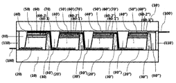
- Figure 1 shows the structure of the first dye-sensitized solar cell
- Figure 2 is an optical interconnection portion manufactured by the present invention
- the overall diagram of the monolithic module structure separated from the electrical conversion layer is shown.
- the structure of the first dye-sensitized solar cell includes a substrate or film 10, a first electrode layer 20, an insulating partition 30, a photoelectrode 40, an electrolyte layer 50, and an insulating layer 60-. 1), the catalyst layer 60-2, the second electrode layer 60, and the interconnection 70, the structure of the monolithic module structure in which the interconnection of the present invention is separated from the photoelectric conversion layer.
- the first dye-sensitized solar cell to the fourth dye-sensitized solar cell are adjacent to each other separated by an insulating partition and connected by an interconnection, and the first conduction of the first and fourth dye-sensitized solar cells
- the leader line is connected to the power source from the layer and the fourth conductive layer.
- the manufacturing method of the dye-sensitized solar cell monolithic module in which the interconnection portion of the present invention is installed separately from the photoelectric conversion layer is as follows.
- a photoresist pattern is formed on a plurality of portions forming an insulating partition on the transparent glass substrate 10, and the first electrode layer 20, 20 ', 20' ', which is a transparent conductive oxide film, is formed on the upper surface of the transparent glass substrate 10. ..) After forming a plurality of the photoresist on the transparent glass substrate 10 to form a plurality of insulating partition formation pattern positions at which the insulating partition can be installed at the same time.
- Silicon oxide paste is applied and fired at the positions of a plurality of patterns provided on the transparent glass substrate, and a plurality of insulating partitions 30, 30 ', 30 " .... are respectively installed at the same time.
- a solid electrolyte (50, 50 ', 50' '.%) on each of the plurality of photoelectrode layers (40, 40', 40 '' ....), respectively, and each solid Each insulating layer (60-1, 60-1 ', 60-1' '.%) over the electrolyte (50, 50', 50 '' .7)
- a plurality of catalyst layers 60-2, 60-2 ', 60-2 " .... and respective second conductive layers 60, 60', 60 " .7) are formed.
- the insulating partition wall installed on the transparent glass substrate is preferably narrower in width from the junction surface to the upper side of the transparent substrate.
- the photoelectrode layer, the solid electrolyte layer, the insulating layer, and the catalyst layer formed in contact with the insulating partition wall are stacked and have a trapezoidal shape.
- a By forming a, to form a V-shaped empty space with a neighboring encapsulation layer or insulating partition.
- the interconnection formed on one side of the insulating partition wall and the photoelectric conversion layer of the neighboring solar cell are not formed.
- the second electrode layer adjacent to the second electrode layer formed on the first dye-sensitized solar cell
- an interconnection made of an anisotropic conductive film is applied to one side which is not in contact with the photoelectric conversion layer of the insulating partition wall.
- each of the dye-sensitized solar cells and interconnects are first coated with an insulator film, covered with an upper transparent glass substrate (10 '), and top and bottom transparent glass. The edge of the substrate is sealed with glass paste.
- an insulating partition for electrical insulation with neighboring cells is formed on a transparent substrate away from the first electrode layer (TCO), and a part of the insulating partition is adjacent to the solar cell.
- the first electrode layer (TCO) of the structure to cover the photoelectrode and the neighboring TCO is not short-circuit, effectively prevent the short circuit between the neighboring TCO, and close the interconnection between the cell and the present invention
- Interconnection structure not only has the advantage that it can be easily manufactured by the screen printing printing method, but also the conductive layer of various materials can be used to connect the catalyst layer and the TCO layer, and the deformation of the shape can be diversified. .
Landscapes
- Engineering & Computer Science (AREA)
- Power Engineering (AREA)
- Chemical & Material Sciences (AREA)
- Chemical Kinetics & Catalysis (AREA)
- Electrochemistry (AREA)
- Microelectronics & Electronic Packaging (AREA)
- Photovoltaic Devices (AREA)
- Hybrid Cells (AREA)
Abstract
태양전지셀은 첫번째로 제1전극층이 절연 기판위에 형성되고, 광전기적 변환 요소가 제1전극층 위에 형성되며, 광전기적 변환요소는 염료가 흡착되고, 전해질층, 절연층이 형성되어 있으며, 촉매층을 가지는 다공성 반도체층에 형성되는 광전기적 변환층을 가지는 제1셀의 제2전극층은 이웃하는 셀의 광전극 변환층과 분리된 인터커넥션으로 연결되는 모노리식 구조의 염료감응 태양전지에 있어서, 이웃하는 셀과의 전기적 절연을 목적으로 하는 절연격벽 부분을 투명기판상에서 하나의 셀의 제1 전극층과 떨어지게 형성하며 동시에 절연격벽의 일부가 이웃하는 하나의 셀의 제1전극층을 덮는 구조로 구성하여 광전극과 이웃하는 TCO가 단락이 되지 않도록 하고 이웃하는 TCO 사이의 단락을 효과적으로 방지하며, 셀과 셀사이의 인터커넥션을 긴밀하게 하는 것으로, 본 발명에 의한 인터커넥션은 스크린프린팅 인쇄방법으로 손쉽게 설치할 수 있으며, 격벽과의 접착력이 우수할 뿐만 아니라 전기 전도성도 뛰어난 장점이 있다.
Description
본 발명은 염료감응 태양전지의 모노리식 구조에 관한 것으로, 태양전지셀의 인터커넥션 전극부분이 이웃하는 태양전지셀의 광전기적 변환층과 분리 되도록 설치한 모노리식 모듈의 셀 연결구조에 관한 것이다.
태양전지 셀을 다수개 연결하여 광전변환효율을 향상시키고자 하는 기술이 개발되고 있다. 염료감응 태양전지 모듈을 구성하는 셀의 구성 및 셀을 연결하는 방식에 따라 W형, Z형, Monolithic 방식 및 집전그리드 방식으로 분류된다.
W형은 셀간 직렬구성의 모듈로서 셀의 제1전극과 인접하는 셀의 제2전극이 동일 전극을 이용하고 한 쌍으로 구성되어 있어 별도의 셀간을 연결하는 인터커넥션 배선이 불필요하다는 장점이 있는 반면, 절반의 셀은 빛이 전해질을 통과하여 광전극에 도달하여 발전한다는 것 때문에 전해질에 의한 빛 흡수 손실이 크다는 단점이 있으며, Z형은 각 단위셀 사이에 격벽을 통한 인터커넥션 배선을 연결하는 방식으로, 단위셀 사이의 Sealing 작업과 셀의 제1전극과 이웃하는 셀의 제2전극을 직렬연결하는 인터커넥션 배선작업을 하기 때문에 소자 제작 공정이 복잡하고 유효면적이 감소하는 단점이 있으며, 집전그리드 방식은 셀간 병렬형 구조의 모듈로서 단위 셀을 분할하지 않고 전도성 기판면에 전류를 수집하여 외부로 취출하기 위한 금속 그리드 배선을 형성하는 방식으로 밀봉된 하나의 대형 셀 내에 다수의 염료감응 태양전지 구조를 수용하는 것으로 소자구조가 가장 간단해 양산성이 좋은 장점이 있으나, 모듈 면적 증가에 따른 집전극의 배선저항 감소를 위한 배선면적이 증가되면 이에 따른 Dead Space가 급격하게 증가하여 효율이 감소하는 단점이 있다.
Monolithic 방식의 모듈구조는 Z형 방식의 발전형으로서, 투명 전도성 기판을 한장만 사용하고 모든 공정을 인라인 공정이 가능하다는 장점이 있어 염료감응 태양전지의 다수개의 셀을 연결하는 방식으로 생산성이 우수한 모듈구조이나, 셀을 연결하는 구성에 있어서 제1셀의 제1전극과 이웃하는 셀의 제1전극이 연결되기 쉽다는 문제점이 지적되어 왔다.
발명의 요약
태양전지 셀 구성은 제1전극층이 투명기판위에 형성되고, 광전기적 변환층이 제1전극층 위에 형성되며, 광전기적 변환층은 염료가 흡착되는 광전극층, 광전극층 위에 전해질층, 절연층이 형성되어 있으며, 절연층 위에 촉매층으로 구성되고 촉매층의 다음으로 제2전극층을 형성한다. 첫번째 셀의 제2전극층은 절연 격벽을 사이에 두고 이웃하는 셀의 제1전극층과 전기적으로 접촉하고 있다. 이러한 모노리식 염료감응 태양전지에 있어서 절연격벽 하단부분이 이웃하는 셀의 제1전극층(TCO)상에 설치되는 구성에 있어서 전기적 단락이 문제점으로 지적되어 왔다.
본 발명에서는 이웃하는 태양전지셀과의 전기적 절연을 목적으로 하는 절연격벽 하단부분을 이웃하는 셀의 제1전극층(TCO) 부분과 떨어지게 투명 기판위에 형성하며 동시에 절연격벽의 하단부분 일부가 이웃하는 태양전지셀의 제 1전극층을 덮는 구조로 구성하여 광전기적 변환층의 제1전극과 이웃하는 셀의 제1 전극층이 단락이 되지 않도록 이웃하는 제1전극층(TCO) 사이의 단락을 효과적으로 방지하며, 셀과 이웃하는 셀 사이의 인터커넥션을 긴밀하게 한다. 또한 인터커넥션이 절연 격벽과 긴밀하게 접착되도록 하면서 스크린프린팅 인쇄방법으로 손쉽게 제조할 수 있는 방법을 제공하는 것이다
도 1. 본 발명의 염료감응 태양전지의 모노리식 모듈 단위셀의 구조
도 2. 본 발명의 염료감응 태양전지의 모노리식 모듈 구조
발명의 상세한 설명 및 구체적인 구현예
본 발명은 모노리식 염료감응 태양전지 모듈의 구조에 관한 것으로 다수개의 태양전지 셀을 전기적으로 연결하여 구성한다. 본 발명의 다수개의 태양전지 셀은 모노리식 염료감응 태양전지 셀의 용도에 따라 적정수로 설계하여 정할 수 있다.
본 발명의 태양전지셀의 모듈구조는 투명기판상에 제1전극층과 광전극층, 전해질층, 절연층, 촉매층으로 구성되는 광전기적 변환층 및 제2전극층으로 구성되는 단위 태양전지셀을 다수 개 형성하고, 각 단위셀을 직렬 연결하는 데 있어 셀사이에는 절연격벽을 형성하며, 각 단위 셀의 제2전극층과 이웃하는 단위 셀의 제1전극층을 연결하는 데 있어 셀사이에 절연격벽이 형성되고 절연격벽을 타고 넘으면서 전기적으로 연결하는 인터커넥션 배선으로 연결하고, 각 단위셀사이 또는 단위셀과 봉지층 사이에 V자 모양의 밀폐공간이 형성되어 연결된 다수개의 태양전지셀의 상부를 투명기판으로 덮은 후 봉지재로 밀봉하는 모노리식 모듈구조로서, 태양전지 셀의 제1전극층과 이웃하는 셀의 제1전극층(TCO)이 단락이 되지 않도록 이웃하는 제1전극층(TCO) 사이의 단락을 효과적으로 방지하며, 셀과 셀사이의 인터커넥션을 긴밀하게 하는 것이다.
본 발명은 제1 염료감응 태양전지 셀의 제2전극층이 이웃하는 제2염료감응 태양전지 셀(cell)의 제1전극층에 접촉하는 구조로 다수개의 염료감응 태양전지 셀(cell)이 연결되는 구조에 있어서, 본 발명은 상기 제1염료감응 태양전지 셀(cell)의 제2전극층과 이웃하는 제2염료감응 태양전지 셀(cell)의 제1전극층을 연결하는 구조로서 인터커넥션을 설치하는 것을 특징으로 한다.
또한, 본 발명은 투명기판상의 절연격벽을 형성하는 부분에 패턴과 제1전극층을 형성하는 단계(a), 패턴이 형성된 부분에 절연 격벽을 형성하는 단계(b), 절연격벽의 일측면하단 제1전극층 위에 광전극층, 전해질층, 절연층, 촉매층으로 구성되는 광전기적 변환층 및 제2전극층을 형성하는 단계(c), 하나의 염료감응 태양전지 셀의 제2전극층과 절연 격벽을 사이에 둔 이웃하는 염료감응 태양전지 셀의 제1전극층을 절연격벽을 타고 넘으면서 전기적으로 연결하는 인터커넥션을 형성하는 단계(d), 하나의 염료감응 태양전지 셀과 봉지재 또는 인터커넥션 사이에 V자 모양의 밀폐공간에 필름포장 또는 절연체 충전 또는 절연체와 광산란 비즈 중 어느 하나의 방식을 적용하는 단계(e), 전체 염료감응 태양전지 셀의 상부를 투명기판으로 덮고, 상하부 투명기판을 봉지재로 밀봉하는 단계(f)로 구성되는, 인터커넥션 부분이 분리 설치된 염료감응 태양전지의 모노리식 모듈구조의 제조방법을 제공한다.
본 발명의 투명기판은 디스플레이용 투명 도전막, 태양전지용 투명도전막을 사용하며, 일반적으로 전기적으로 절연체인 유리 (bare glass, soda-lime)에 전도성 물질을 코팅하여 제조한다. 유리는 전기적으로 절연체로 상온에서 10-10~10-11(Ωcm)-1의 전기전도도를 갖고 있는데, 이러한 절연체인 유리에 높은 투광성을 유지한 채 전기전도성을 부여하기 위하여 유리의 표면에 다양한 TCO(투명전도산화막)이나 금속을 코팅하여 전도성을 부여한 것이 바로 투명전도코팅이고 이에 의하여 제조되고 있는 것이 투명도전성 유리이다. 본 발명에서는 상기 제1 염료감응 태양전지 셀과 이웃하는 제2의 염료감응 태양전지 셀의 사이에 격벽을 설치하는 부분에는 투명전도산화막(TCO)을 전기적으로 절연한다. 절연격벽 부분은 제1전극층(TCO) 부분과 떨어지게 투명기판위에 형성하며 동시에 절연격벽의 하단일부가 이웃하는 태양전지셀의 제1전극층 (TCO)을 덮는 구조로 구성하여 셀의 광전기적 변환층의 광전극과 이웃하는 셀의 제1 전극층(TCO)이 단락이 되지 않도록 구성된다.
이와 같이 본 발명의 도전성 유리의 투명전도막은 격벽이 설치되는 부분에 패턴을 형성하는 방법으로 PR을 이용하여 마스크에 형성된 이미지를 노광시켜 PR을 현상하고 이후에 에천트를 이용하여 이를 식각하여 패턴을 형성하는 방법, FTO를 사용하는 경우에는 FTO가 내 화학성이 우수하여 에천트를 이용한 케미컬 에칭이 불가능하기 때문에 레이저를 이용하여 패턴을 형성하는 방법을 사용할 수 있으며, 유리기판 상면에서 투명전도 산화막이 형성되지 않는 부분에 포토레지스트 패턴을 형성하고, 상기 유리기판의 상면에 투명전도 산화막을 형성한 후 상기 유리기판 상의 포토레지스트를 제거하는 방법을 사용한다.
본 발명은 투명유리기판상의 패턴이 형성된 부분에 셀간 절연층인 격벽을 우선 설치한다. 이웃하는 셀과의 전기적 절연을 목적으로 하는 절연격벽 하단부분을 셀의 제1전극층(TCO) 부분과 떨어지게 투명기판위에 형성하며 동시에 절연격벽의 하단 일부가 이웃하는 셀의 제1전극층 (TCO)을 덮는 구조로 형성하여 광전극과 이웃하는 TCO가 단락이 되지 않도록 하여 이웃하는 셀의 제1전극층(TCO) 사이의 단락을 효과적으로 방지하는 역할을 담당한다.
셀(Cell)간 절연격벽은 전해질층의 산화환원 물질의 이동을 저지하는 기능을 가지며, 절연격벽은 제1염료감응 태양전지 셀의 제1전극층과 이웃하는 제2염료감응 태양전지 셀의 제1전극층과의 단락이 발생하는 것을 방지한다. 따라서 셀(cell)간 절연격벽에 의하여 각 광전변환소자가 구획되고, 절연격벽에 의해 전해질층의 산화환원 물질이 셀(cell)간 절연격벽내를 통과할 수 없는 정도로 치밀한 막인 것이 바람직하다.
여기에서 치밀한 막이란, 인접하는 셀(cell)간을 산화환원물질이 통과할 수 없는 막이라면 좋고, 예를들면 독립기포의 다공체도 포함된다. 예를 들면 절연수지 필름재를 들 수 있고, 산화규소, 산화불소, 산화아연, 산화납, 산화비스무스, 산화티탄, 산화알루미늄, 산화마그네슘 등을 들 수 있다. 셀(cell)간 절연격벽의 형성방법은 제1, 2 염료감응 태양전지 셀사이에 형성된 패턴부분 상에 절연격벽을 스크린 인쇄법, 잉크젯법 등의 기판상의 반도체입자를 함유하는 페이스트(paste)를 도포하고, 그 후 소성하는 방법을 들 수 있다.
투명유리기판상의 셀 패턴이 형성된 부분에 셀간 절연격벽의 외측으로 인터커넥션 배선 형성, 설치한다. 본 발명의 인터커넥션 배선은 제1염료감응 태양전지 셀의 상부에 설치되는 제2전극층과 이웃하는 제2염료감응 태양전지 셀의 하부에 설치되는 제1전극층의 전기적 연결이 이루어지도록 연결된다. 인터커넥션 배선에 의한 전기적 연결은 절연층 격벽의 일측 외부측면, 즉 제1 염료감응 태양전지 셀의 제1전극층과 접하지 않는 격벽의 일측 외부측면을 따라 연결된다. 인터커넥션 배선은 도전성 입자가 분산된 필름을 사용할 수 있다.
본 발명의 인터커넥션에 적용되는 도전성 입자가 분산된 필름은 바람직하게는 이방성 도전성 필름(Anisotropic Conductive Film)일 수 있고, 도전성 입자는 금속분말입자, 도전성 고분자 입자, 또는 절연수지 입자에 도전체가 코팅된 입자일 수 있으며, 상기 필름은 상기 도전성 입자보다 크기가 작거나 같은 스페이스(Spacer) 입자를 더 포함하여 인터커넥션의 탄력성 및 절연층 격벽과의 접착력을 강화할 수 있다. 상기 스페이스(Spacer) 입자는 탄력성을 가진 고무성분이면 좋고 바람직하게는 부타디엔류의 고무성분을 사용할 수 있다.
상기 제1염료감응 태양전지 셀과 제2염료감응 태양전지 셀 사이에 설치되는 절연격벽의 일측면, 즉 인터커넥션이 형성, 설치되는 격벽의 반대측 경사면을 따라 제1 염료감응 태양전지 셀의 광전극층, 전해질층, 절연층 촉매층으로 구성되는 광전기적 변환층을 형성한다.
본 발명의 제1염료감응 태양전지 셀의 광전극층은 다공성 반도체층으로서 공지의 산화티탄, 산화아연 등의 반도체를 1종 또는 2종류 이상 조합하여 사용할 수 있으며, 바람직하게는 변환효율, 안정성의 점에서 산화티탄을 사용할 수 있다. 반도체층의 형태는 입자 상태, 막상 상태 등의 다양한 형태의 것을 이용할 수 있으며, 다공성 반도체층을 기판상에 형성하는 방법으로는 구체적으로 스크린 인쇄법, 잉크젯(ink jet)법 등의 기판상에 반도체 입자를 함유하는 페이스트(paste)를 도포하고, 그 후 소성하는 방법을 사용한다. 광전변환 효율을 향상시키기 위해서는 염료를 다공성 반도체층에 많이 흡착시키는 것이 필요하고 그러기 위해서는 다공성 반도체층의 표면적이 큰 것이 바람직하나, 본 발명에서는 광대역 파장의 햇빛을 흡수하기 위하여 2종류 이상의 염료를 포함하는 것이며, 염료를 다공성 반도체층에 효과적으로 흡착시키기 위해서, 다공성 반도체 입자의 크기를 수광면으로부터 작고, 크고, 작은 순서로 배치하는 것을 특징으로 한다. 본 발명의 반도체 입자는 구체적으로 1nm에서 500nm의 평균입경을 가지며 표면적이 10~200㎡/g 정도가 바람직하다. 본 발명의 다공성 반도체층의 건조 및 소성은 일반공기 분위기 하에서 50~800℃ 범위내에서, 10초~4시간 정도로 건조 및 소성하며, 이 건조 및 소성은 단일의 온도로 1회 또는 온도를 변화시키면서 2회 이상 행할 수 있다.
본 발명의 제1염료감응 태양전지 셀의 염료는 다공성 반도체층에 흡착되어 광전변환의 기능을 수행한다. 본 발명의 다공성 반도체층은 입사광을 최대한으로 이용할 수 있도록 수광면으로부터 작은입자의 다공성 반도체, 큰 입자의 다공성 반도체, 작은 입자의 다공성 반도체의 순서로 다층구조를 형성하며, 각 입자크기에 맞추어 유기색소, 금속착체색소를 선택하여 흡착시킨다. 본 발명에서는 종래보다 몰흡광계수가 현저히 향상된 Ru계 염료(동진쎄미켐 공개번호 10-2008-77765)를 사용할 수 있다. 또한 본 발명에서 사용되는 염료는 아조(azo)계 염료, 메로시아닌계 염료, 퀴논계 염료, 퀴논 이민(quinone imine)계 염료, 퀴나크리돈(quinacridone)계 염료, 스쿠알릴륨계 염료, 시아닌(Cyanine)계 염료, 메로시아닌계 염료, 트리페닐메탄계 염료, 키산텐계 염료, 포르피린계 염료, 페닐렌계 염료, 인디고(indigo)계 염료, 나프탈로시아닌(naphthalocyanine)계 염료 등 유기염료와, 전이금속에 기능기가 배위결합한 형태의 금속착체 염료를 사용할 수 있다. 금속착체 염료는 Cu. Ni. Fe, Co, V, Sn, Si, Ti, Ge, Cr, Zn, Ru, Mg, Al, Pb, Mn, Y, Zr, Nb, Sb, La, W, Pt, Ta, Ir, Pd, Os, Ga, Tb, Eu, Rb, Bi, Se, As, Sc, Ag, Cd, Hf, Re, Au, Ac, Tc, Te, 등의 금속분자가 배위결합된 형태의 것이 사용되어 지며, 일반적으로 유기색소가 금속착체염료에 비하여 흡광계수가 크다.
본 발명의 전해질층은 액체전해질, 고체전해질, 겔전해질 중 고체전해질 또는 겔전해질을 사용하는 것이 바람직하다. 액체전해질은 산화환원 효율면에서 높은 성능을 발휘할 수 있으나, 전해질의 누설 등 봉지구조가 필수적으로 필요하여 본 발명에 의한 모노리식 모듈 구조에서 제조단계에서 문제점이 있다. 본 발명에서 사용되는 고체전해질은 전자, 홀(hole), 이온(ion)을 수송할 수 있는 캐리어(career) 수송재료로 염료감응 태양전지의 전해질로서 이용할 수 있고, 유동성이 없는 것이면 좋다. 구체적으로는 폴리카르바졸(poly carbazol) 등의 홀(hole) 수송재, 테트라니트로프로올레논 등의 전자 수송재, 폴리롤(poly roll) 등의 도전성 폴리머, 액체 전해질을 고분자화합물에 의하여 고체화한 고분자 전해질, 요오드화동, 티오시안산동 등의 p형 반도체, 용융소금을 포함하는 액체 전해질을 미립자에 의하여 고체화한 전해질을 사용할 수 있다. 그리고 본 발명에 사용되는 겔전해질은 통상 전해질과 겔화제를 포함한다. 겔화제로서는 예를 들면 가교폴리아크릴수지 유도체나 가교 폴리 아크릴로니트릴(poly acrylonitrile) 유도체, 폴리알킬렌옥시드(polyalkylene oxide) 유도체, 실리콘 수지류, 측쇄에 함질소 복소환식 4급 화합물 구조를 가지는 폴리머 등의 고분자 겔화제를 사용할 수 있다. 본 발명의 산화환원제는 예를 들면, I-/I3-계, Br2-/Br3-계, Fe2-/Fe3-계, 퀴논(quinone)/하이드로퀴논(hydroquinone)계 등의 산화환원 동을 들 수 있다. 구체적으로는 요오드화 리튬(LiI), 요오드화나트륨(NaI), 요오드화칼륨(KI), 요오드화칼슘(CaI) 등의 금속 요오드화물과 테트라에칠암모니윰아이오다이드(TEAI), 테트라프로필암모니윰아이오다이드(TPAI), 테트라부칠암모니윰아이오다이드(TBAI), 테트라헥실암모니윰아이오다이드(THAI) 등의 테트라알킬암모늄, 브롬화리튬(LiBr), 브롬화나트륨(NaBr), 브롬화칼륨(KBr), 브롬화칼슘(CaBr2)등의 금속브롬화물 등이 사용될 수 있다.
본 발명의 절연층을 구성하는 재료로서는 알루미나(Al2O3),지르코니아(ZrO), 실리카(SiO2)등 산화물 나노입자로 이루어지는 군에서 선택되며, 공지의 방법을 사용하여 성형한다.
본 발명의 촉매층은 제2전극 아래에 형성되며, 촉매층을 구성하는 재료로서는 캐리어(career) 수송층의 산화환원 반응을 활성화시키게 하는 물질이바람직하다. 예를 들면, 백금(Pt), 카본블랙(Carbon Black), 그래파이트(Graphite), 유리(Glass) 탄소, 아모르퍼스(Amorphous) 탄소, 하드카본(Hard Carbon), 소프트카본(Soft Carbon), 카본나노튜브(Carbon Nano Tube)가 사용될 수 있다. 촉매층은 백금을 사용하는 것이 바람직하며, 백금을 사용하는 경우, PVC법, 증착법, 스퍼터링(Spattering)법 등의 공지기술에 의하여 형성할 수 있고, 카본(Carbon)을 이용하는 경우 카본(Carbon)을 용매로 분산하고 페이스트상으로 한 것을 스크린 인쇄법이라고 하는 도포법에 의하여 도포막을 형성하고 건조 및 소성을 행하여 형성할 수 있다.
본 발명의 제2전극층은 제1전극층과 동일한 방법으로 제조할 수 있으며, 금속, 합금, 금속 산화물을 단독 또는 선택적으로 다수 세트를 합쳐서 이용할 수 있고, 증착법, 스퍼터(Sputter) 등에 따라서 형성할 수 있다. 또한 제2전극층 무기재료 또는 수지재료를 스크린 인쇄법에 의하여 도포하고 건조 및 소성하는 방법으로 제조할 수 있다.
본 발명의 제1전극층과 제2전극층의 외측으로 투명 기판 및 필름을 성형하여 염료감응 태양전지 셀을 보호하는 동시에 고정시키는 구성을 가지며, 각 염료감응 태양전지 셀 사이 빈공간에는 필름으로 도포하거나 절연체를 채우는 구성을 하거나, 빛 산란 비즈를 채움으로서 각 염료감응 태양전지 셀에 보다 많은 빛이 모아질 수 있도록 하는 구성을 추가할 수 있다.
본 발명은 다수개의 염료감응 태양전지 셀을 전기적으로 연결한 후 각 다수개의 염료감응 태양전지 셀과 인터커넥션 사이의 V자 모양의 빈공간에는 절연체로 채우고 상부 투명유리기판(10')으로 덮고 상하부 투명유리기판의 테두리를 글래스 플릿 페이스트로 밀봉하거나, 다수개의 염료감응 태양전지 셀을 전기적으로 연결한 후 다수개의 염료감응 태양전지 셀과 인터커넥션 사이의 V자 모양의 빈공간에 빛 산란 비즈를 채운 후 상부 투명유리기판(10')으로 덮고 상하부 투명유리기판의 테두리를 글래스 플릿 페이스트로 밀봉할 수 있다.
본 발명의 염료감응 태양전지 모노리식 모듈 구조의 실시예를 도면을 참조하면, 도면 1은 제1염료감응 태양전지 셀의 구조를 나타낸 것이고, 도면 2는 본 발명에 의하여 제조된 인터커넥션 부분이 광전기적 변환층과 분리 설치된 모노리식 모듈구조의 전체 도면을 나타낸 것이다.
도면 1에서 제1염료감응 태양전지 셀의 구조는 기판 또는 필름(10), 제1전극층(20), 절연 격벽(30), 광전극(40), 전해질층(50), 절연층(60-1), 촉매층(60-2), 제2전극층(60), 인터커넥션(70)의 구조로 되었고, 도면 2를 참조하면서 본 발명의 인터커넥션이 광전기적 변환층과 분리설치된 모노리식 모듈구조를 살펴보면, 제1 염료감응 태양전지 셀 내지 제4염료감응 태양전지 셀이 이웃하면서 절연 격벽으로 분리되고 인터커넥션으로 연결되어 있음을 알 수 있으며, 제1 및 제4 염료감응 태양전지 셀의 제1도전층 및 제4도전층으로부터 리더선이 연결되어 전원으로 연결되는 구조이다.
이하, 실시예에 의하여 본 발명의 인터커넥션 부분이 광전기적 변환층과 분리설치된 염료감응 태양전지 모노리식 모듈의 제조방법을 도면을 참조하여 상세히 설명하며, 본 실시예에 의하여 본 발명의 기술사상 및 기술구성이 한정되는 것은 아니다.
실시예 1
본 발명의 인터커넥션 부분이 광전기적 변환층과 분리설치된 염료감응 태양전지 모노리식 모듈의 제조방법은 다음과 같다.
투명유리기판(10)상의 절연격벽을 형성하는 다수개의 부분에 포토레지스터 패턴을 형성하고, 투명유리기판(10)의 상면에 투명전도 산화막인 제1전극층(20, 20', 20''....) 다수개를 형성한 후 상기 투명유리기판(10) 상의 포토레지스트를 제거하여 절연격벽을 설치할 수 있는 다수개의 절연격벽 형성 패턴 위치를 동시에 형성한다.
투명유리기판 상에 설치된 다수개의 패턴의 위치에 산화규소 페이스트를 도포하고 소성하여 절연 격벽(30, 30', 30''....) 다수개를 각각 동시에 설치한다. 절연 격벽(30, 30', 30''....)을 사이에 두고 셀의 제 1전극층 위에 염료가 흡착되는 다공성 산화티탄 광전극층(40, 40', 40''....) 다수개를 각각 형성하고, 다수개의 광전극층(40, 40', 40''....) 각각의 위에 고체전해질(50, 50', 50''....) 각각 형성하며, 각각의 고체전해질(50, 50', 50''....) 위에 각각의 절연층(60-1, 60-1', 60-1''....) 촉매층(60-2, 60-2', 60-2''....) 및 각각의 제2전도층(60, 60', 60''....) 다수개를 형성한다. 투명유리기판 상에 설치되는 절연격벽은 투명기판과 접합면으로부터 상부로 갈수록 폭이 좁아지는 것이 바람직하며, 절연격벽과 접하여 형성되는 광전극층, 고체전해질층, 절연층, 촉매층이 적층된 후 사다리꼴 모양을 형성하여, 이웃하는 봉지층 또는 절연격벽과 V자 모양의 빈공간을 형성하게 된다. 상기 V자 모양의 빈공간을 절연재 등으로 채움으로써 절연격벽의 일측면에 형성되는 인터커넥션과 이웃하는 태양전지셀의 광전기적 변환층이 접하지 않도록 형성된다.
투명유리기판 상에 설치된 제1 전극층(20, 20', 20''....) 각각을 바탕으로 하여 상부로 가면서, 광전극층(40, 40', 40''....), 전해질층(50, 50',50''....), 촉매층(60-1, 60-1', 60-1''....) 및 제2전극층(60, 60', 60''....)은 폭을 점점 좁혀가는 전체적으로 사다리꼴 모양의 광전변환소자층을 형성한다.
다수개의 절연 격벽 (30, 30', 30''....)을 기둥으로 하여 다수개의 광전기적 변환층을 형성한 후, 제1 염료감응 태양전지 셀의 상부에 형성된 제2전극층과 이웃하는 제2 염료감응 태양전지 셀의 하부에 형성된 제1전극층을 전기적으로 연결하기 위하여, 이방성 도전성 필름으로 된 인터커넥션을 절연격벽의 광전기적 변환층과 접촉하지 않는 일측면으로 도포하여 형성한다.
다수개의 인터커넥션으로 다수개의 염료감응 태양전지 셀을 전기적으로 연결한 후 각 다수개의 염료감응 태양전지 셀과 인터커넥션을 절연체 필름으로 일차 도포한 후 상부투명유리기판 (10')으로 덮고 상하부 투명유리기판의 테두리를 글래스플릿 페이스트로 밀봉한다.
부호의 설명
10, 10' : 투명기판, 투명유리기판 또는 필름
20, 20', 20'' .... : 제1 전극층
30, 30', 30'' .... : 절연 격벽
40, 40', 40'' .... : 광전극층
50, 50', 50'' .... : 전해질층
60, 60', 60'' .... : 제2 전극층
60-1, 60-1', 60-1'' .... : 절연층
60-2, 60-2', 60-2'' .... : 촉매층
70, 70', 70'' .... : 인터커넥션
80, 80', 80'' .... : 필름도포층, 절연체 도포층, 절연체 또는 광산란비즈 도포층
100, 100' ..... : 전극연결 리드선
110, 110' ..... : 봉지층
염료감응 태양전지의 모노리식 모듈구조에 있어서 이웃하는 셀과의 전기적 절연을 목적으로 하는 절연격벽을 제1전극층(TCO) 부분과 떨어지게 투명기판위에 형성하며 동시에 절연격벽의 일부가 이웃하는 태양전지셀의 제1전극층(TCO)을 덮는 구조로 구성하여 광전극과 이웃하는 TCO가 단락이 되지 않도록 하고 이웃하는 TCO 사이의 단락을 효과적으로 방지하며, 셀과 셀사이의 인터커넥션을 긴밀하게 하는 한편 본 발명의 인터커넥션 구조는 스크린 프린팅 인쇄방법으로 손쉽게 제조할 수 있다는 장점이 있을 뿐만 아니라, 촉매층과 TCO층의 연결에 다양한 재질의 전도층을 사용할 수 있고, 형상의 변형도 다양화 할 수 있는 장점이 있다.
Claims (5)
- 투명기판상에 제1전극층과 광전극층, 전해질층, 절연층, 촉매층으로 구성되는 광전기적 변환층 및 제2전극층으로 구성되는 단위 태양전지셀을 다수개 형성하고, 각 단위셀 사이에는 절연격벽을 형성하며, 각 단위셀의 제2전극층과 이웃하는 단위셀의 제1전극층을 절연격벽을 타고 넘으면서 전기적으로 연결하는 인터커넥션 배선으로 연결하고, 각 단위셀 사이 또는 단위셀과 봉지층 사이에 V자 모양의 밀폐공간이 형성되어 연결된 다수개의 태양전지셀의 상부를 투명기판으로 덮은 후 봉지층으로 밀봉하는 인터커넥션 부분이 광전기적 변환층과 분리 설치된 염료감응 태양전지의 모노리식 모듈구조.
- 청구항 1에 있어서, 절연격벽은 투명기판상에서 하나의 셀의 제1 전극층(TCO)과 떨어지게 형성하며 동시에 절연격벽의 일부가 이웃하는 하나의 셀의 제1전극층(TCO)을 일부 덮는 구조로 구성하여, 하나의 셀의 광전기적 변환층과 이웃하는 제1전극층(TCO)이 단락이 되지 않는 것을 특징으로 하는 인터커넥션 배선 부분이 광전기적 변환층과 분리 설치된 염료감응 태양전지의 모노리식 모듈구조.
- 청구항 1에서, 인터커넥션은 이방성 도전성 필름 또는 도전성 입자가 분산된 필름 또는 도전성 입자보다 크기가 작거나 같은 스페이스 입자를 더 포함하는 필름 중에서 선택되는 것을 특징으로 하는 인터커넥션 배선부분이 광전기적 변환층과 분리 설치된 염료감응 태양전지의 모노리식 모듈구조.
- 청구항 1에서, 염료감응 태양전지 셀과 봉지층 또는 이웃하는 인터커넥션 배선 사이에 V자 모양의 밀폐공간을 절연체 필름으로 도포하거나, 절연체를 채우거나, 빛 산란 비즈로 채우는 방식 중 어느 하나의 방식으로 구성하는 것을 특징으로 하는 인터커넥션 배선부분이 광전기적 변환층과 분리 설치된 염료감응 태양전지의 모노리식 모듈구조.
- 투명기판상의 절연 격벽을 형성하는 부분에 패턴과 제1전극층을 형성하는 단계(a), 패턴이 형성된 부분에 절연 격벽을 형성하는 단계(b), 절연격벽의 일측면하단 제1전극층위에 광전극층, 전해질층, 절연층, 촉매층으로 구성되는 광전기적 변환층 및 제2전극층을 형성하는 단계(c), 하나의 염료감응 태양전지 셀의 제2전극층 절연 격벽을 사이에 둔 이웃하는 타 염료감응 태양전지 셀의 제1전극층을 절연 격벽을 타고 넘으면서 전기적으로 연결하는 인터커넥션을 형성하는 단계(d), 하나의 염료감응 태양전지 셀과 봉지재 또는 인터커넥션, 사이에 V자 모양의 밀폐공간에 필름포장 또는 절연체 충전 또는 절연체와 광산란 비즈 중 어느 하나의 방식을 적용하는 단계(e), 전체 염료감응 태양전지 셀의 상부를 투명기판으로 덮고, 상하부 투명기판을 봉지재로 밀봉하는 단계(f)로 구성되는, 인터커넥션 배선부분이 분리 설치된 염료감응 태양전지의 모노리식 모듈구조의 제조방법.
Applications Claiming Priority (4)
| Application Number | Priority Date | Filing Date | Title |
|---|---|---|---|
| KR10-2010-0105246 | 2010-10-27 | ||
| KR20100105246 | 2010-10-27 | ||
| KR10-2011-0109327 | 2011-10-25 | ||
| KR1020110109327A KR20120044256A (ko) | 2010-10-27 | 2011-10-25 | 인터커넥션 부분이 분리 설치된 염료감응 태양전지의 모노리식 모듈구조 |
Publications (2)
| Publication Number | Publication Date |
|---|---|
| WO2012057514A2 true WO2012057514A2 (ko) | 2012-05-03 |
| WO2012057514A3 WO2012057514A3 (ko) | 2012-06-21 |
Family
ID=45994550
Family Applications (1)
| Application Number | Title | Priority Date | Filing Date |
|---|---|---|---|
| PCT/KR2011/008013 Ceased WO2012057514A2 (ko) | 2010-10-27 | 2011-10-26 | 인터커넥션 부분이 분리 설치된 염료감응 태양전지의 모노리식 모듈구조 |
Country Status (1)
| Country | Link |
|---|---|
| WO (1) | WO2012057514A2 (ko) |
Family Cites Families (5)
| Publication number | Priority date | Publication date | Assignee | Title |
|---|---|---|---|---|
| JP4606799B2 (ja) * | 2004-07-22 | 2011-01-05 | 株式会社フジクラ | 光電変換素子 |
| JP5052768B2 (ja) * | 2005-06-29 | 2012-10-17 | 学校法人東京理科大学 | 太陽電池モジュールおよびその製造方法 |
| JP2008065998A (ja) * | 2006-09-04 | 2008-03-21 | Fujikura Ltd | 太陽電池モジュール及びその製造方法 |
| JP5085078B2 (ja) * | 2006-09-04 | 2012-11-28 | 株式会社フジクラ | 太陽電池モジュール及びその製造方法 |
| KR20100028327A (ko) * | 2008-09-04 | 2010-03-12 | 주식회사 이건창호 | 염료감응형 태양전지 모듈 프레임 |
-
2011
- 2011-10-26 WO PCT/KR2011/008013 patent/WO2012057514A2/ko not_active Ceased
Also Published As
| Publication number | Publication date |
|---|---|
| WO2012057514A3 (ko) | 2012-06-21 |
Similar Documents
| Publication | Publication Date | Title |
|---|---|---|
| US8143516B2 (en) | Dye-sensitized solar cell module | |
| US8933328B2 (en) | Dye-sensitized solar cell module and method of producing the same | |
| CN102460821B (zh) | 湿式太阳能电池模块 | |
| JP4278615B2 (ja) | 色素増感型太陽電池及び色素増感型太陽電池モジュール | |
| US20130206227A1 (en) | Transparent conductive film, method of producing the same, photoelectric conversion apparatus, and electronic apparatus | |
| EP2214250A1 (en) | Electrode substrate for photoelectric conversion device, method for manufacturing electrode substrate for photoelectric conversion device, and photoelectric conversion device | |
| WO2011009631A1 (en) | A method of manufacturing working electrodes for dye sensitised solar cells | |
| CN118102735A (zh) | 钙钛矿太阳能电池串联组件及其制备方法 | |
| JP2005285472A (ja) | 光電変換装置 | |
| JP2006019278A (ja) | 光電変換素子を利用した染料感応太陽電池 | |
| KR101152544B1 (ko) | 광전 변환 소자용 전극, 이의 제조 방법 및 이를 포함하는 광전 변환 소자 | |
| JP2008177022A (ja) | 色素増感型太陽電池の電極および色素増感型太陽電池 | |
| CN105513812B (zh) | 一种石墨烯太阳能电池及其制备方法 | |
| JP2004164950A (ja) | 電極基板、光電変換素子、並びに色素増感太陽電池 | |
| JP4892186B2 (ja) | 色素増感太陽電池および色素増感太陽電池モジュール | |
| JP5364999B2 (ja) | 酸化物半導体電極用積層体、酸化物半導体電極、色素増感型太陽電池、および色素増感型太陽電池モジュール | |
| JP4754892B2 (ja) | 光電変換素子および色素増感型太陽電池モジュール | |
| KR20120044256A (ko) | 인터커넥션 부분이 분리 설치된 염료감응 태양전지의 모노리식 모듈구조 | |
| WO2012057514A2 (ko) | 인터커넥션 부분이 분리 설치된 염료감응 태양전지의 모노리식 모듈구조 | |
| JP4497999B2 (ja) | 色素増感太陽電池 | |
| US20150122322A1 (en) | Wet-type solar cell and wet-type solar cell module | |
| EP3133622B1 (en) | Photoelectric conversion element, dye-sensitized solar cell, and dye-sensitized solar cell module | |
| WO2013015067A1 (ja) | 光電変換装置、電子機器および建築物 | |
| JP2007172915A (ja) | 光電変換装置 | |
| JP5251149B2 (ja) | 酸化物半導体電極用積層体、酸化物半導体電極、および色素増感型太陽電池モジュール |
Legal Events
| Date | Code | Title | Description |
|---|---|---|---|
| 121 | Ep: the epo has been informed by wipo that ep was designated in this application |
Ref document number: 11836606 Country of ref document: EP Kind code of ref document: A2 |
|
| NENP | Non-entry into the national phase |
Ref country code: DE |
|
| 32PN | Ep: public notification in the ep bulletin as address of the adressee cannot be established |
Free format text: NOTING OF LOSS OF RIGHTS PURSUANT TO RULE 112(1) EPC (EPO FORM 1205 DATED 03.07.2013) |
|
| 122 | Ep: pct application non-entry in european phase |
Ref document number: 11836606 Country of ref document: EP Kind code of ref document: A2 |