WO2012057074A1 - 薄膜トランジスタおよびこれを備える表示パネル - Google Patents
薄膜トランジスタおよびこれを備える表示パネル Download PDFInfo
- Publication number
- WO2012057074A1 WO2012057074A1 PCT/JP2011/074425 JP2011074425W WO2012057074A1 WO 2012057074 A1 WO2012057074 A1 WO 2012057074A1 JP 2011074425 W JP2011074425 W JP 2011074425W WO 2012057074 A1 WO2012057074 A1 WO 2012057074A1
- Authority
- WO
- WIPO (PCT)
- Prior art keywords
- electrode
- wiring
- source
- drain
- gate electrode
- Prior art date
- Legal status (The legal status is an assumption and is not a legal conclusion. Google has not performed a legal analysis and makes no representation as to the accuracy of the status listed.)
- Ceased
Links
Images








Classifications
-
- H—ELECTRICITY
- H10—SEMICONDUCTOR DEVICES; ELECTRIC SOLID-STATE DEVICES NOT OTHERWISE PROVIDED FOR
- H10D—INORGANIC ELECTRIC SEMICONDUCTOR DEVICES
- H10D30/00—Field-effect transistors [FET]
- H10D30/60—Insulated-gate field-effect transistors [IGFET]
- H10D30/67—Thin-film transistors [TFT]
- H10D30/6729—Thin-film transistors [TFT] characterised by the electrodes
-
- G—PHYSICS
- G02—OPTICS
- G02F—OPTICAL DEVICES OR ARRANGEMENTS FOR THE CONTROL OF LIGHT BY MODIFICATION OF THE OPTICAL PROPERTIES OF THE MEDIA OF THE ELEMENTS INVOLVED THEREIN; NON-LINEAR OPTICS; FREQUENCY-CHANGING OF LIGHT; OPTICAL LOGIC ELEMENTS; OPTICAL ANALOGUE/DIGITAL CONVERTERS
- G02F1/00—Devices or arrangements for the control of the intensity, colour, phase, polarisation or direction of light arriving from an independent light source, e.g. switching, gating or modulating; Non-linear optics
- G02F1/01—Devices or arrangements for the control of the intensity, colour, phase, polarisation or direction of light arriving from an independent light source, e.g. switching, gating or modulating; Non-linear optics for the control of the intensity, phase, polarisation or colour
- G02F1/13—Devices or arrangements for the control of the intensity, colour, phase, polarisation or direction of light arriving from an independent light source, e.g. switching, gating or modulating; Non-linear optics for the control of the intensity, phase, polarisation or colour based on liquid crystals, e.g. single liquid crystal display cells
- G02F1/133—Constructional arrangements; Operation of liquid crystal cells; Circuit arrangements
- G02F1/136—Liquid crystal cells structurally associated with a semi-conducting layer or substrate, e.g. cells forming part of an integrated circuit
- G02F1/1362—Active matrix addressed cells
- G02F1/1368—Active matrix addressed cells in which the switching element is a three-electrode device
Definitions
- the present invention relates to a thin film transistor and a display panel including the same.
- a thin film transistor (hereinafter also referred to as “TFT”) is used to drive each pixel.
- the TFT includes a semiconductor layer.
- an a-Si thin film (amorphous silicon thin film) is generally used. By disposing the source electrode and the drain electrode, a part of the a-Si thin film serves as a channel region.
- Patent Document 1 discloses a TFT having a U-shaped source electrode and an I-shaped drain electrode.
- the source electrode, the channel region, and the drain electrode are arranged in a straight line.
- off-leakage current When light enters the channel region of the a-Si thin film, a photocurrent caused by electron-hole pairs is generated.
- a photocurrent is generated only by the incidence of light regardless of the original instruction to the TFT means that a leak current flows when the TFT is turned off.
- Such a leakage current is hereinafter referred to as “off-leakage current”.
- off-leakage current increases, phenomena such as flicker and crosstalk occur. As a result, the display quality of the display panel is degraded.
- an object of the present invention is to provide a TFT capable of suppressing the flow of off-leakage current. It is another object of the present invention to provide a display panel that can suppress flicker, crosstalk, and the like caused by off-leakage current.
- a TFT according to the present invention includes a substrate, a gate electrode formed on the surface of the substrate, a gate insulating film formed so as to cover the upper side of the gate electrode, and the gate insulating film.
- the channel region is at a position avoiding the extension of the source wiring.
- the channel region is at a position avoiding the extension of the drain wiring.
- the channel region is located at a position avoiding the extension of the source wiring and at a position avoiding the extension of the drain wiring, the light that travels by being repeatedly reflected enters the channel region. Without going out of the TFT. Therefore, it is possible to suppress the off-leakage current caused by the photocurrent in the channel region from flowing.
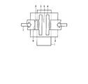
- FIG. 6 is an enlarged view of the TFT shown in FIG. 5.
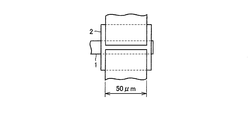
- FIG. 7 is an enlarged view of the TFT shown in FIG. 6. It is a graph of the experimental result in I-shaped TFT. It is a graph of the 1st experimental result in U-shaped TFT.
- FIG. 14 is a cross-sectional view taken along the line XIV-XIV in FIG. 13.
- FIG. 14 is a cross-sectional view taken along line XV-XV in FIG. 13.
- TFT in Embodiment 2 It is a top view of TFT in Embodiment 2 based on this invention. It is a top view of TFT in Embodiment 3 based on this invention. It is a top view of the display panel in Embodiment 4 based on this invention. It is an enlarged view of the pixel contained in the display panel in Embodiment 4 based on this invention.
- the inventors examined the cause of off-leakage current.
- the inventors thought that off-leakage current may be generated by light incident on the channel region of the a-Si thin film for some reason.
- the channel region overlaps with the black matrix portion of the display panel, light from the front side of the display panel is blocked by the black matrix portion.
- the channel region is disposed at a position overlapping the gate electrode that does not transmit light, the channel region is at a position where light from the backlight device cannot directly enter.
- the inventors assumed a model shown in FIG. 1 and performed a simulation to examine how light from the backlight device travels. In FIG.
- FIG. 2 shows a cross-sectional view taken along the line II-II in FIG.
- FIG. 2 shows how light entering from a backlight device (not shown) travels.
- the width of the overlapping portion between the gate electrode 1 and the source electrode 3 or the drain electrode 4 was 5.75 ⁇ m per location.
- the black matrix portion 6 is located above the TFT so as to cover the projection area of the TFT. The reflectance of the black matrix portion 6 was assumed to be zero.
- the light 7 from the backlight device hits the lower surfaces of the source electrode 3 and the drain electrode 4 and then reflects, then hits the upper surface of the gate electrode 1 and further reflects.
- the light 7 is incident on the channel region 5 after being repeatedly reflected between the lower surfaces of the source electrode 3 and the drain electrode 4 and the upper surface of the gate electrode 1. Light incident on the channel region 5 from other paths was not observed.
- the light incident on the channel region 5 is light that travels by being repeatedly reflected between the lower surfaces of the source electrode 3 and the drain electrode 4 and the upper surface of the gate electrode 1. .
- the region where the gate electrode 1 and the source electrode 3 or the drain electrode 4 overlap is a region 8 in which multiple reflection of the light 7 can occur (hereinafter referred to as “multiple reflection region”).
- the size of the width 9 of the portion where the source electrode 3 or the drain electrode 4 protrudes from the end of the gate electrode 1 means the size of the entrance of light into the multiple reflection region 8. The greater the width 9 is, the more light can enter the multiple reflection region 8. As shown in FIG. 4, when the width 9 is small, the amount of light entering the multiple reflection region 8 is also small.
- FIGS. 5 and 6 Two types of TFTs as shown in FIGS. 5 and 6 were prepared.
- the enlarged view of each TFT in FIGS. 5 and 6 is shown in FIGS. 7 and 8, respectively.
- the TFT shown in FIGS. 5 and 7 is a so-called I-shaped TFT.
- the TFT shown in FIGS. 6 and 8 is a so-called U-shaped TFT.
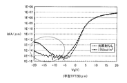
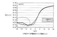
- FIG. 9 shows the relationship with Id.
- the potential Vd applied to the drain electrode is 4.1V.
- the graph of FIG. 9 shows two types of curves, that is, when light is not irradiated and when light of 1750 cd / m 2 is irradiated. As shown by an ellipse in FIG. 9, there is an open portion between these two curves.
- the size of the opening in the vertical direction corresponds to the magnitude of off-leakage current due to light incident on the channel region.
- the U-shaped TFT shown in FIG. 8 has a structure in which the I-shaped electrode 15 and the U-shaped electrode 16 face each other.
- the width of the portion where the I-shaped electrode 15 protrudes from the end of the gate electrode 1 is 6 ⁇ m.
- the width of the portion where the U-shaped electrode 26 protrudes from the end of the gate electrode 1 is 26 ⁇ m.
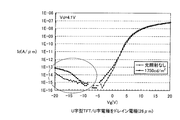
- FIG. 10 shows the relationship between the voltage Vg of the gate electrode and the current Id flowing through the drain electrode when the U-shaped electrode 16 is used as the drain electrode in the U-shaped TFT. 10 also shows two curves as in FIG.
- FIG. 11 shows the relationship between the voltage Vg of the gate electrode and the current Id flowing through the drain electrode when the I-shaped electrode 15 is used as the drain electrode in the U-shaped TFT. Also in FIG. 11, two curves are shown as in FIG.
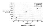
- FIG. 12 is a graph showing the relationship between the wiring width and the amount of off-leakage current per unit channel width based on the results shown in FIGS.
- FIG. 12 shows the level of off-leakage current Id for three wiring width values under the condition that the gate electrode potential Vg is 15 V and the drain electrode potential is 4.1 V. It can be seen that the off-leakage current Id increases as the wiring width increases.
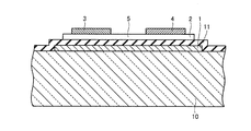
- FIG. 14 is a cross-sectional view taken along the line XIV-XIV in FIG.
- FIG. 15 is a cross-sectional view taken along line XV-XV in FIG.
- the thin film transistor 101 includes a substrate 10, a gate electrode 1 formed on the surface of the substrate 10, a gate insulating film 11 formed to cover the upper side of the gate electrode 1, and a semiconductor layer formed on the gate insulating film 11. 2, the source electrode 3 and the drain electrode 4 formed so as to be spaced apart from each other with the channel region 5 interposed therebetween when viewed in plan on the upper side of the semiconductor layer 2, and the gate electrode 1 viewed in plan view from the source electrode 3
- a source wiring 13 extending outward and a drain wiring 14 extending outward from the gate electrode 1 when viewed in plan from the drain electrode 4 are provided.
- the channel region 5 is at a position avoiding the extension of the source wiring 13.
- the channel region 5 is at a position avoiding the extension of the drain wiring 14.
- the light 7 from the backlight device enters from below as indicated by an arrow in FIG. 14, and travels by being repeatedly reflected between the drain electrode 4 and the gate electrode 1.
- FIG. 14 shows the progress of the light 7 on the lower side of the drain electrode 4, similarly, the light 7 travels by being repeatedly reflected between the source electrode 3 and the gate electrode 1 on the lower side of the source electrode 3. To do.
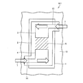
- the path of the light 7 at this time is shown in a plan view as shown by arrows in FIG.
- the light 7 enters along the longitudinal direction of each of the source wiring 13 and the drain wiring 14, proceeds on the extension of each of the source wiring 13 and the drain wiring 14 as it is, and passes through the source electrode 3 and the drain electrode 4.
- the light 7 that travels by being repeatedly reflected exits the TFT 101 after traversing the source electrode 3 and the drain electrode 4.
- the channel region 5 is located at a position avoiding the extension of the source wiring 13 and is located at a position avoiding the extension of the drain wiring 14, so that light that travels with repeated reflections is transmitted to the channel region. 5 goes out of the TFT 101 without entering.
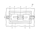
- FIG. 17 A comparative example is shown in FIG. Assuming a TFT 100 having a channel region 5 on the extension of the source wiring 13 and the drain wiring 14 as shown in FIG. 17, the light 7 is reflected between the source wiring 13 and the drain wiring 14 and the gate electrode 1. Although it is likely to enter the channel region 5 after being repeated, such a situation can be avoided in the TFT 101 in this embodiment. Thus, the incidence of light on the channel region 5 can be suppressed. Accordingly, since generation of off-leakage current due to photocurrent in the channel region can be avoided, it is possible to suppress the off-leakage current from flowing in the TFT 101 in this embodiment.
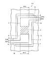
- FIG. 18 shows the names of the dimensions of each part in the TFT 101.
- the lateral width of the source electrode 3 in FIG. 18 is W1S
- the lateral width of the drain electrode 4 is W1D.
- W1S and W1D are widths facing the channel region 5, respectively.
- the width of the source wiring 13 is W2S
- the width of the drain wiring 14 is W2D.
- the width W2S of the source wiring and the width W2D of the drain wiring are minimum widths according to the design rule.
- the semiconductor layer 2 is formed along the source wiring 13 and the drain wiring 14 in a portion where the source wiring 13 and the drain wiring 14 respectively come out from the region of the gate electrode 1 when viewed in plan.
- the semiconductor layer protrusions 2 a and 2 b protrude from the region of the gate electrode 1, respectively, and the semiconductor layer protrusions 2 a and 2 b have portions protruding from both sides in the width direction of the source wiring 13 and the drain wiring 14. 13 and the drain wiring 14, and the protrusion amounts ⁇ Wa and ⁇ Wb per side of the portion protruding to both sides in the width direction are preferably the minimum width in the design rule.
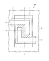
- a semiconductor layer 2 is arranged on the upper side of the gate electrode 1, and the semiconductor layer 2 has a shape in which two locations protrude from a rectangle.
- the semiconductor layer 2 has a shape of a vertically long rectangle with the upper left protruding toward the left and the lower right protruding toward the right.
- the source electrode 3 and the drain electrode 4 are both L-shaped.
- a channel region 5 i is formed in a part of the semiconductor layer 2 as a portion where the source electrode 3 and the drain electrode 4 face each other with a narrow interval. Because the source electrode 3 and the drain electrode 4 are L-shaped, the channel region 5i has a polygonal line shape and an inverted S-shape.
- the channel region 5i is located at a position avoiding the extension of the source wiring 13 and at a position avoiding the extension of the drain wiring 14, so that light that travels repeatedly by reflection is transmitted. Exits from the TFT 102 without entering the channel region 5. Therefore, also in the TFT 102 in this embodiment, off-leakage current can be suppressed as in the first embodiment.
- a semiconductor layer 2 is arranged on the upper side of the gate electrode 1, and the semiconductor layer 2 has a shape in which two locations protrude from a rectangle.
- the semiconductor layer 2 has a shape in which an upper left corner of a vertically long rectangle protrudes toward the left and a central portion on the right side protrudes toward the right.
- the source electrode 3 has a substantially U shape
- the drain electrode 4 has an I shape.
- the source electrode 3 is substantially U-shaped, the source line 13 extends not to the center of the source electrode 3 but to a position biased to one side.
- a channel region 5j is formed in a part of the semiconductor layer 2 as a portion where the source electrode 3 and the drain electrode 4 face each other at a narrow interval.
- the source electrode 3 is disposed so as to surround the tip of the drain electrode 4. As a result, the channel region 5j is substantially U-shaped.
- the TFT 103 in this embodiment is formed on the substrate 10, the gate electrode 1 formed on the surface of the substrate 10, the gate insulating film 11 formed so as to cover the upper side of the gate electrode 1, and the gate insulating film 11.
- a source line 13 extending to the outside of the gate electrode 1 and a drain line 14 extending to the outside of the gate electrode 1 when viewed in plan from the drain electrode 4 are provided.
- the channel region 5j is at a position avoiding at least one of the extension of the source line 13 and the extension of the drain line 14. In the TFT 103 exemplified here, specifically, the channel region 5 j is at a position avoiding the extension of the source wiring 13.
- the channel region 5j is located at a position avoiding the extension of the source wiring 13, the light that travels by being repeatedly reflected between the source wiring 13 and the gate electrode 1 is the channel region 5j. It goes out of the TFT 103 without being incident on the TFT 103.
- the channel region 5j since a part of the channel region 5j is on the extension of the drain electrode 14, light that travels by being repeatedly reflected between the drain electrode 14 and the gate electrode 1 may enter the channel region 5j. There is.
- the channel region is arranged so as to avoid the extension of one of the source wiring and the drain wiring, the light entry into the channel region can be greatly reduced. Therefore, although less effective than the first and second embodiments, the off-leak current can be suppressed to some extent also in the TFT 103 in this embodiment.
- the source electrode 3 is substantially U-shaped and the drain electrode 4 is I-shaped.
- the source electrode and the drain electrode may be reversed. In that case, the same effect can be obtained.
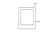
- the display panel 201 has a display area 201d.
- FIG. 22 shows an enlarged view of one pixel in the display area 201d.
- the display panel 201 includes a pixel electrode 211 and a driving element 212 for driving the pixel electrode 211.
- the drive element 212 is any of the thin film transistors (TFTs) described in the first embodiment.
- the present invention can be used for a thin film transistor and a display panel including the thin film transistor.
Landscapes
- Physics & Mathematics (AREA)
- Nonlinear Science (AREA)
- Engineering & Computer Science (AREA)
- Microelectronics & Electronic Packaging (AREA)
- Mathematical Physics (AREA)
- Chemical & Material Sciences (AREA)
- Crystallography & Structural Chemistry (AREA)
- General Physics & Mathematics (AREA)
- Optics & Photonics (AREA)
- Thin Film Transistor (AREA)
- Liquid Crystal (AREA)
Abstract
TFT(101)は、基板(10)と、基板(10)の表面に形成されたゲート電極(1)と、ゲート電極(1)の上側を覆うように形成されたゲート絶縁膜と、上記ゲート絶縁膜上に形成された半導体層(2)と、半導体層(2)の上側において平面的に見てチャネル領域(5)を挟んで互いに離隔するように形成されたソース電極(3)およびドレイン電極(4)と、ソース電極(3)から平面的に見てゲート電極(1)の外側へと延在するソース配線(13)と、ドレイン電極(4)から平面的に見てゲート電極(1)の外側へと延在するドレイン配線(14)とを備える。チャネル領域(5)は、ソース配線(13)の延長上を避けた位置にあり、かつ、ドレイン配線(14)の延長上を避けた位置にある。
Description
本発明は、薄膜トランジスタおよびこれを備える表示パネルに関するものである。
液晶表示パネルなどの表示パネルにおいて、各画素を駆動するために薄膜トランジスタ(以下「TFT」ともいう。)が用いられる。TFTは半導体層を備える。TFTの半導体層としては一般的にa-Si薄膜(非晶質シリコン薄膜)が用いられる。ソース電極およびドレイン電極が配置されることにより、a-Si薄膜の一部がチャネル領域として働くこととなる。
特開2009-86118号公報(特許文献1)においては、U字形のソース電極とI字形のドレイン電極とを備えたTFTが開示されている。特許文献1に開示されたTFTにおいては、ソース電極、チャネル領域およびドレイン電極が一直線上に並んで配置されている。
a-Si薄膜のチャネル領域に光が入射すると電子-正孔対に起因した光電流が発生する。本来のTFTへの指示とは無関係に光の入射のみによって光電流が発生してしまうということは、TFTのオフ時にリーク電流が流れることを意味する。このようなリーク電流を以下「オフリーク電流」というものとする。オフリーク電流が増加することによって、フリッカ、クロストークといった現象が発生する。その結果、表示パネルとしては表示品質が低下する。
そこで、本発明は、オフリーク電流が流れることを抑制することができるようなTFTを提供することを目的とする。さらに、オフリーク電流に起因して生じていたフリッカ、クロストークなどといった現象を抑えることができる表示パネルを提供することを目的とする。
上記目的を達成するため、本発明に基づくTFTは、基板と、上記基板の表面に形成されたゲート電極と、上記ゲート電極の上側を覆うように形成されたゲート絶縁膜と、上記ゲート絶縁膜上に形成された半導体層と、上記半導体層の上側において平面的に見てチャネル領域を挟んで互いに離隔するように形成されたソース電極およびドレイン電極と、上記ソース電極から平面的に見て上記ゲート電極の外側へと延在するソース配線と、上記ドレイン電極から平面的に見て上記ゲート電極の外側へと延在するドレイン配線とを備える。上記チャネル領域は、上記ソース配線の延長上を避けた位置にある。上記チャネル領域は、上記ドレイン配線の延長上を避けた位置にある。
本発明によれば、チャネル領域は、ソース配線の延長上を避けた位置にあり、かつ、ドレイン配線の延長上を避けた位置にあるので、反射を繰り返して進行する光はチャネル領域に入射することなくTFTの外に出る。したがって、チャネル領域での光電流に起因するオフリーク電流が流れることを抑制することができる。
(発明者らによる検討)
発明者らは、オフリーク電流の原因について検討した。発明者らは、a-Si薄膜のチャネル領域に何らかの事情で光が入射することによってオフリーク電流が生じているのではないかと考えた。しかし、チャネル領域は、表示パネルのブラックマトリックス部と重なっているので、表示パネルの表側からの光はブラックマトリックス部により遮光されている。また、チャネル領域は、光を通さないゲート電極と重なるような位置に配置されているので、バックライト装置からの光が直接入射することができない位置にある。したがって、一見すると光はチャネル領域には入射しないように思われる。そこで、発明者らは、図1に示すモデルを想定し、バックライト装置からの光がどのように進行するか調べるためにシミュレーションを行なった。図1においては、縦長長方形のゲート電極1の上側に横長長方形の半導体層2が横断するように配置され、さらにその上側にソース電極3、ドレイン電極4が配置されている。半導体層2の中央がチャネル領域5となっている。図1におけるII-II線に関する矢視断面図を図2に示す。図2ではバックライト装置(図示せず)から進入する光がどのように進行するかが示されている。このシミュレーションにおいては、ゲート電極1とソース電極3またはドレイン電極4との重なり部分の幅は1ヶ所当たり5.75μmとした。図2に示すようにTFTの上方にはTFTの投影領域を被覆するようにブラックマトリックス部6が位置している。ブラックマトリックス部6の反射率は0であるものとした。
発明者らは、オフリーク電流の原因について検討した。発明者らは、a-Si薄膜のチャネル領域に何らかの事情で光が入射することによってオフリーク電流が生じているのではないかと考えた。しかし、チャネル領域は、表示パネルのブラックマトリックス部と重なっているので、表示パネルの表側からの光はブラックマトリックス部により遮光されている。また、チャネル領域は、光を通さないゲート電極と重なるような位置に配置されているので、バックライト装置からの光が直接入射することができない位置にある。したがって、一見すると光はチャネル領域には入射しないように思われる。そこで、発明者らは、図1に示すモデルを想定し、バックライト装置からの光がどのように進行するか調べるためにシミュレーションを行なった。図1においては、縦長長方形のゲート電極1の上側に横長長方形の半導体層2が横断するように配置され、さらにその上側にソース電極3、ドレイン電極4が配置されている。半導体層2の中央がチャネル領域5となっている。図1におけるII-II線に関する矢視断面図を図2に示す。図2ではバックライト装置(図示せず)から進入する光がどのように進行するかが示されている。このシミュレーションにおいては、ゲート電極1とソース電極3またはドレイン電極4との重なり部分の幅は1ヶ所当たり5.75μmとした。図2に示すようにTFTの上方にはTFTの投影領域を被覆するようにブラックマトリックス部6が位置している。ブラックマトリックス部6の反射率は0であるものとした。
図2に示すように、バックライト装置からの光7はソース電極3およびドレイン電極4の下面に当たって反射した後に、ゲート電極1の上面に当たってさらに反射している。光7はソース電極3およびドレイン電極4の下面とゲート電極1の上面との間で反射を何度か繰り返した後にチャネル領域5に入射している。チャネル領域5に対してこれ以外の経路からの光の入射は見られなかった。
したがって、チャネル領域5に対して入射する光の原因は、ソース電極3およびドレイン電極4の下面とゲート電極1の上面との間で反射を繰り返して進行してくる光であるということがわかった。
平面図である図1に光7の進路を記入すると、図3に示すようになる。図3に示すようにゲート電極1とソース電極3またはドレイン電極4とが重なっている領域は光7の多重反射が起こり得る領域(以下「多重反射領域」という。)8となっている。ソース電極3またはドレイン電極4がゲート電極1の端から突出する部分の幅9の大きさは、多重反射領域8への光の入口の大きさを意味する。この幅9が大きければ大きいほど多くの光が多重反射領域8へ進入することができる。図4に示すように幅9が小さくなっている場合は、多重反射領域8に進入する光の量も小さくなる。
(実験)
シミュレーション結果を踏まえて、発明者らは、チャネル領域への光入射の量には、ソース電極またはドレイン電極がゲート電極の端から突出する部分の幅や形状が関係することを知得したが、さらに確認するために、発明者らは、実際の装置で実験を行なった。
シミュレーション結果を踏まえて、発明者らは、チャネル領域への光入射の量には、ソース電極またはドレイン電極がゲート電極の端から突出する部分の幅や形状が関係することを知得したが、さらに確認するために、発明者らは、実際の装置で実験を行なった。
図5、図6に示すような2種類のTFTを用意した。図5、図6の各TFTを拡大したところを図7、図8にそれぞれ示す。図5、図7に示したTFTはいわゆるI字型TFTである。図6、図8に示したTFTはいわゆるU字型TFTである。
図7に示すように、I字型TFTにおいて電極がゲート電極の端から突出する部分の幅を50μmとした場合の、ゲート電極に印加する電位Vgと、ドレイン電極に流れる単位チャネル幅当たりの電流Idとの関係を図9に示す。このときドレイン電極に印加される電位Vdは4.1Vである。図9のグラフは、光を照射しない場合と、1750cd/m2の光を照射した場合との2通りの曲線を示している。図9中に楕円で示すように、これらの2本の曲線の間には開いている部分がある。この開きの上下方向の大きさが、チャネル領域に入射する光によるオフリーク電流の大きさに相当する。
図8に示したU字型TFTにおいては、I字形電極15とU字形電極16とが互いに対向する構造となっている。I字形電極15がゲート電極1の端から突出する部分の幅は6μmである。U字形電極26がゲート電極1の端から突出する部分の幅は26μmである。
U字型TFTにおいてU字形電極16をドレイン電極とした場合の、ゲート電極の電圧Vgと、ドレイン電極に流れる電流Idとの関係を図10に示す。図10においても、図9と同様に2通りの曲線を示す。
U字型TFTにおいてI字形電極15をドレイン電極とした場合の、ゲート電極の電圧Vgと、ドレイン電極に流れる電流Idとの関係を図11に示す。図11においても、図9と同様に2通りの曲線を示す。
図9~図11に示した結果から、配線幅と単位チャネル幅当たりのオフリーク電流の量との関係についてグラフ化したものを図12に示す。図12では、ゲート電極の電位Vgは15V、ドレイン電極の電位は4.1Vの条件下で、3通りの配線幅の値に対してオフリーク電流Idがどの程度であるかが示される。配線幅が大きくなるとオフリーク電流Idも大きくなっていることがわかる。
以上のことを知得した発明者らは、TFTにおいて上記課題を解決する発明として本発明をなした。本発明の実施の形態について以下に説明する。
(実施の形態1)
図13~図15を参照して、本発明に基づく実施の形態1における薄膜トランジスタ(TFT)について説明する。図13におけるXIV-XIV線に関する矢視断面図を図14に示す。図13におけるXV-XV線に関する矢視断面図を図15に示す。
図13~図15を参照して、本発明に基づく実施の形態1における薄膜トランジスタ(TFT)について説明する。図13におけるXIV-XIV線に関する矢視断面図を図14に示す。図13におけるXV-XV線に関する矢視断面図を図15に示す。
薄膜トランジスタ101は、基板10と、基板10の表面に形成されたゲート電極1と、ゲート電極1の上側を覆うように形成されたゲート絶縁膜11と、ゲート絶縁膜11上に形成された半導体層2と、半導体層2の上側において平面的に見てチャネル領域5を挟んで互いに離隔するように形成されたソース電極3およびドレイン電極4と、ソース電極3から平面的に見てゲート電極1の外側へと延在するソース配線13とドレイン電極4から平面的に見てゲート電極1の外側へと延在するドレイン配線14とを備える。チャネル領域5は、ソース配線13の延長上を避けた位置にある。なおかつ、チャネル領域5は、ドレイン配線14の延長上を避けた位置にある。
本実施の形態では、バックライト装置からの光7は図14に矢印で示すように下方から進入し、ドレイン電極4とゲート電極1との間で反射を繰り返して進行する。図14ではドレイン電極4の下側における光7の進行について示しているが、ソース電極3の下側においても同様に、光7はソース電極3とゲート電極1との間で反射を繰り返して進行する。この際の光7の進路を平面的に示すと図16に矢印で示すとおりである。光7は、ソース配線13、ドレイン配線14の各々の長手方向に沿って進入し、そのままソース配線13、ドレイン配線14の各々の延長上を進行してソース電極3、ドレイン電極4を通過する。反射を繰り返して進行する光7は、図14、図16に示すように、ソース電極3、ドレイン電極4を横断し終えるとTFT101の外に出る。
本実施の形態では、チャネル領域5は、ソース配線13の延長上を避けた位置にあり、かつ、ドレイン配線14の延長上を避けた位置にあるので、反射を繰り返して進行する光はチャネル領域5に入射することなくTFT101の外に出る。
比較例を図17に示す。図17に示すようにソース配線13、ドレイン配線14の延長上にチャネル領域5がある構成のTFT100を想定した場合、光7はソース配線13、ドレイン配線14とゲート電極1との間で反射を繰り返した末にチャネル領域5に入射しやすいが、本実施の形態におけるTFT101では、そのような事態を避けることができる。こうして、チャネル領域5への光の入射を抑制することができる。したがって、チャネル領域での光電流に起因するオフリーク電流の発生を避けることができるので、本実施の形態におけるTFT101ではオフリーク電流が流れることを抑制することができる。
TFT101における各部の寸法の呼び名を図18に示す。図18におけるソース電極3の横方向の幅はW1Sであり、ドレイン電極4の横方向の幅はW1Dである。W1S,W1Dはそれぞれチャネル領域5に対向する幅である。ソース配線13の幅はW2Sであり、ドレイン配線14の幅はW2Dである。本実施の形態におけるTFT101では、ソース配線の幅W2Sおよびドレイン配線の幅W2Dが設計ルール上の最小幅となっていることが好ましい。この構成を採用することにより、ソース電極またはドレイン電極とゲート電極との間に入射してくる光を最小限に抑えることができるので、光リーク電流の発生を抑えることができる。
本実施の形態におけるTFT101では、半導体層2は、平面的に見て、ソース配線13およびドレイン配線14がゲート電極1の領域からそれぞれ出ていく部分において、ソース配線13およびドレイン配線14に沿ってゲート電極1の領域からそれぞれ突出する半導体層突出部2a,2bを有し、半導体層突出部2a,2bは、ソース配線13およびドレイン配線14の幅方向の両側にはみ出す部分を有するようにソース配線13およびドレイン配線14より広い幅となっており、前記幅方向の両側にはみ出す部分の片側当たりのはみ出し量ΔWa,ΔWbは、設計ルール上の最小幅となっていることが好ましい。この構成を採用することにより、ゲート電極の外側にはみ出す半導体幅はソース電極側、ドレイン電極側とも最小となるので、さらに光リーク電流の発生を抑えることができる。
(実施の形態2)
図19を参照して、本発明に基づく実施の形態2におけるTFT102について説明する。ゲート電極1の上側に半導体層2が配置されており、半導体層2は長方形から2ヶ所が突出した形状をしている。図19においては、半導体層2は、縦長長方形の左上が左に向かって突出し、右下が右に向かって突出した形状である。ソース電極3とドレイン電極4とはいずれもL字形である。ソース電極3とドレイン電極4とが狭い間隔で対向する部分として半導体層2の一部にチャネル領域5iが形成されている。ソース電極3とドレイン電極4とがL字形であることに起因して、チャネル領域5iは折れ線状かつ逆S字形状となっている。
図19を参照して、本発明に基づく実施の形態2におけるTFT102について説明する。ゲート電極1の上側に半導体層2が配置されており、半導体層2は長方形から2ヶ所が突出した形状をしている。図19においては、半導体層2は、縦長長方形の左上が左に向かって突出し、右下が右に向かって突出した形状である。ソース電極3とドレイン電極4とはいずれもL字形である。ソース電極3とドレイン電極4とが狭い間隔で対向する部分として半導体層2の一部にチャネル領域5iが形成されている。ソース電極3とドレイン電極4とがL字形であることに起因して、チャネル領域5iは折れ線状かつ逆S字形状となっている。
本実施の形態におけるTFT102においても、チャネル領域5iは、ソース配線13の延長上を避けた位置にあり、かつ、ドレイン配線14の延長上を避けた位置にあるので、反射を繰り返して進行する光はチャネル領域5に入射することなくTFT102の外に出る。したがって、本実施の形態におけるTFT102においても、実施の形態1と同様にオフリーク電流を抑制することができる。
(実施の形態3)
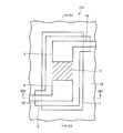
図20を参照して、本発明に基づく実施の形態3におけるTFT103について説明する。ゲート電極1の上側に半導体層2が配置されており、半導体層2は長方形から2ヶ所が突出した形状をしている。図20においては、半導体層2は、縦長長方形の左上が左に向かって突出し、右辺中央部が右に向かって突出した形状である。ソース電極3は略U字形状であり、ドレイン電極4はI字形状である。ソース電極3は略U字形状であるが、ソース配線13は、ソース電極3の中心ではなく一方に偏った位置に連なって延在している。ソース電極3とドレイン電極4とが狭い間隔で対向する部分として半導体層2の一部にチャネル領域5jが形成されている。ソース電極3はドレイン電極4の先端部を取り囲むように配置されている。その結果、チャネル領域5jは略U字形状となっている。
図20を参照して、本発明に基づく実施の形態3におけるTFT103について説明する。ゲート電極1の上側に半導体層2が配置されており、半導体層2は長方形から2ヶ所が突出した形状をしている。図20においては、半導体層2は、縦長長方形の左上が左に向かって突出し、右辺中央部が右に向かって突出した形状である。ソース電極3は略U字形状であり、ドレイン電極4はI字形状である。ソース電極3は略U字形状であるが、ソース配線13は、ソース電極3の中心ではなく一方に偏った位置に連なって延在している。ソース電極3とドレイン電極4とが狭い間隔で対向する部分として半導体層2の一部にチャネル領域5jが形成されている。ソース電極3はドレイン電極4の先端部を取り囲むように配置されている。その結果、チャネル領域5jは略U字形状となっている。
本実施の形態におけるTFT103は、基板10と、基板10の表面に形成されたゲート電極1と、ゲート電極1の上側を覆うように形成されたゲート絶縁膜11と、ゲート絶縁膜11上に形成された半導体層2と、半導体層2の上側において平面的に見てチャネル領域5を挟んで互いに離隔するように形成されたソース電極3およびドレイン電極4と、ソース電極3から平面的に見てゲート電極1の外側へと延在するソース配線13と、ドレイン電極4から平面的に見てゲート電極1の外側へと延在するドレイン配線14とを備える。チャネル領域5jは、ソース配線13の延長上とドレイン配線14の延長上とのうちの少なくとも一方を避けた位置にある。ここで例示するTFT103においては、具体的には、チャネル領域5jはソース配線13の延長上を避けた位置にある。
本実施の形態におけるTFT103においても、チャネル領域5jは、ソース配線13の延長上を避けた位置にあるので、ソース配線13とゲート電極1との間で反射を繰り返して進行する光はチャネル領域5jに入射することなくTFT103の外に出る。本実施の形態では、チャネル領域5jの一部はドレイン電極14の延長上にあるので、ドレイン電極14とゲート電極1との間で反射を繰り返して進行する光はチャネル領域5jに入射する可能性がある。しかし、このようにチャネル領域がソース配線とドレイン配線の一方の延長上を避けるのみの配置であっても、チャネル領域への光の進入は大幅に低減することができる。したがって、実施の形態1,2に比べて効果が劣るものの、本実施の形態におけるTFT103においても、ある程度はオフリーク電流を抑制することができる。
なお、本実施の形態では、ソース電極3が略U字形状であって、ドレイン電極4がI字形状であるものとして説明したが、ソース電極とドレイン電極とが逆であってもよい。その場合も、同様の効果を得ることができる。
(実施の形態4)
図21を参照して、本発明に基づく実施の形態4における表示パネルについて説明する。この表示パネル201は、表示領域201dを有する。表示領域201d内の1つの画素を拡大したところを図22に示す。この表示パネル201は、画素電極211と、画素電極211を駆動するための駆動素子212を備える。駆動素子212は、実施の形態1で説明したいずれかの薄膜トランジスタ(TFT)である。
図21を参照して、本発明に基づく実施の形態4における表示パネルについて説明する。この表示パネル201は、表示領域201dを有する。表示領域201d内の1つの画素を拡大したところを図22に示す。この表示パネル201は、画素電極211と、画素電極211を駆動するための駆動素子212を備える。駆動素子212は、実施の形態1で説明したいずれかの薄膜トランジスタ(TFT)である。
本実施の形態における表示パネルでは、駆動素子としての各TFTにおいて、チャネル領域での光電流に起因するオフリーク電流の発生を避けることができるので、各TFTではオフリーク電流が流れることを抑制することができる。したがって、この表示パネルでは、良好な画像を表示することができる。
なお、今回開示した上記実施の形態はすべての点で例示であって制限的なものではない。本発明の範囲は上記した説明ではなくて請求の範囲によって示され、請求の範囲と均等の意味および範囲内でのすべての変更を含むものである。
本発明は、薄膜トランジスタおよびこれを備える表示パネルに利用可能である。
1 ゲート電極、2 半導体層、2a,2b 半導体層突出部、3 ソース電極、4 ドレイン電極、5,5i,5j チャネル領域、6 ブラックマトリックス部、7 光、8 多重反射領域、9 幅、10 基板、11 ゲート絶縁膜、13 ソース配線、14 ドレイン配線、15 I字形電極、16 U字形電極、100 (比較例としての)TFT、101,102,103 (本発明に基づく)TFT、201 表示パネル、201d 表示領域、211 画素電極、212 駆動素子。
Claims (5)
- 基板(10)と、
前記基板の表面に形成されたゲート電極(1)と、
前記ゲート電極の上側を覆うように形成されたゲート絶縁膜(11)と、
前記ゲート絶縁膜上に形成された半導体層(2)と、
前記半導体層の上側において平面的に見てチャネル領域(5)を挟んで互いに離隔するように形成されたソース電極(3)およびドレイン電極(4)と、
前記ソース電極から平面的に見て前記ゲート電極の外側へと延在するソース配線(13)と、
前記ドレイン電極から平面的に見て前記ゲート電極の外側へと延在するドレイン配線(14)とを備え、
前記チャネル領域は、前記ソース配線の延長上と前記ドレイン配線の延長上とのうちの少なくとも一方を避けた位置にある、薄膜トランジスタ。 - 前記チャネル領域は、前記ソース配線の延長上と前記ドレイン配線の延長上とのいずれも避けた位置にある、請求項1に記載の薄膜トランジスタ。
- 前記ソース配線の幅および前記ドレイン配線の幅が設計ルール上の最小幅となっている、請求項1または2に記載の薄膜トランジスタ。
- 前記半導体層は、平面的に見て、前記ソース配線および前記ドレイン配線が前記ゲート電極の領域からそれぞれ出ていく部分において、前記ソース配線および前記ドレイン配線に沿って前記ゲート電極の領域からそれぞれ突出する半導体層突出部を有し、
前記半導体層突出部は、前記ソース配線および前記ドレイン配線の幅方向の両側にはみ出す部分を有するように前記ソース配線および前記ドレイン配線より広い幅となっており、前記幅方向の両側にはみ出す部分の片側当たりのはみ出し量は、設計ルール上の最小幅となっている、請求項1から3のいずれかに記載の薄膜トランジスタ。 - 請求項1から4のいずれかに記載の薄膜トランジスタを備える、表示パネル。
Applications Claiming Priority (2)
| Application Number | Priority Date | Filing Date | Title |
|---|---|---|---|
| JP2010-244217 | 2010-10-29 | ||
| JP2010244217 | 2010-10-29 |
Publications (1)
| Publication Number | Publication Date |
|---|---|
| WO2012057074A1 true WO2012057074A1 (ja) | 2012-05-03 |
Family
ID=45993782
Family Applications (1)
| Application Number | Title | Priority Date | Filing Date |
|---|---|---|---|
| PCT/JP2011/074425 Ceased WO2012057074A1 (ja) | 2010-10-29 | 2011-10-24 | 薄膜トランジスタおよびこれを備える表示パネル |
Country Status (1)
| Country | Link |
|---|---|
| WO (1) | WO2012057074A1 (ja) |
Citations (2)
| Publication number | Priority date | Publication date | Assignee | Title |
|---|---|---|---|---|
| JP2003167261A (ja) * | 2001-11-30 | 2003-06-13 | Sharp Corp | 液晶表示装置 |
| JP2010014921A (ja) * | 2008-07-03 | 2010-01-21 | Epson Imaging Devices Corp | 表示装置 |
-
2011
- 2011-10-24 WO PCT/JP2011/074425 patent/WO2012057074A1/ja not_active Ceased
Patent Citations (2)
| Publication number | Priority date | Publication date | Assignee | Title |
|---|---|---|---|---|
| JP2003167261A (ja) * | 2001-11-30 | 2003-06-13 | Sharp Corp | 液晶表示装置 |
| JP2010014921A (ja) * | 2008-07-03 | 2010-01-21 | Epson Imaging Devices Corp | 表示装置 |
Similar Documents
| Publication | Publication Date | Title |
|---|---|---|
| CN101009333B (zh) | 半导体装置 | |
| JP5034529B2 (ja) | 電気光学装置用基板及び電気光学装置、並びに電子機器 | |
| CN101131519A (zh) | 电光装置用基板、电光装置以及电子设备 | |
| JP5157319B2 (ja) | 電気光学装置及び電子機器 | |
| JP2004054033A (ja) | アクティブマトリクス基板、電気光学装置、電子機器 | |
| JP5003366B2 (ja) | 電気光学装置及びその製造方法、並びに電子機器 | |
| JP4349406B2 (ja) | 電気光学装置用基板及び電気光学装置、並びに電子機器 | |
| JP2012069842A (ja) | 表示装置 | |
| JP4935404B2 (ja) | 電気光学装置用基板及びその製造方法、並びに電気光学装置及び電子機器 | |
| JP3914753B2 (ja) | アクティブマトリクス型液晶表示装置およびスイッチング素子 | |
| JP5428141B2 (ja) | 電気光学装置、及びこれを備えた電子機器 | |
| JP5176434B2 (ja) | 電気光学装置及び電子機器 | |
| JP2002122889A (ja) | 電気光学装置及び投射型表示装置 | |
| JP5371377B2 (ja) | 表示装置 | |
| WO2012057074A1 (ja) | 薄膜トランジスタおよびこれを備える表示パネル | |
| JP2013080185A (ja) | 液晶表示装置 | |
| JP2009139417A (ja) | 電気光学装置及びその製造方法並びに電子機器 | |
| JP4123245B2 (ja) | 電気光学装置及び電子機器 | |
| US8384836B2 (en) | Liquid crystal display device | |
| JP2010129733A (ja) | 薄膜トランジスタ及び電気光学装置並びに電子機器 | |
| JP5098682B2 (ja) | 電気光学装置及びその製造方法、並びに電子機器 | |
| JP2009053477A (ja) | 電気光学装置及び電子機器 | |
| JP2009115883A (ja) | 電気光学装置及び電子機器 | |
| JP4395807B2 (ja) | 電気光学装置用基板及び電気光学装置、並びに電子機器 | |
| JP4269658B2 (ja) | 電気光学装置及びその製造方法並びに電子機器 |
Legal Events
| Date | Code | Title | Description |
|---|---|---|---|
| 121 | Ep: the epo has been informed by wipo that ep was designated in this application |
Ref document number: 11836208 Country of ref document: EP Kind code of ref document: A1 |
|
| NENP | Non-entry into the national phase |
Ref country code: DE |
|
| 122 | Ep: pct application non-entry in european phase |
Ref document number: 11836208 Country of ref document: EP Kind code of ref document: A1 |
|
| NENP | Non-entry into the national phase |
Ref country code: JP |