WO2012057056A1 - 情報表示用パネルの製造方法及び情報表示用パネル - Google Patents
情報表示用パネルの製造方法及び情報表示用パネル Download PDFInfo
- Publication number
- WO2012057056A1 WO2012057056A1 PCT/JP2011/074392 JP2011074392W WO2012057056A1 WO 2012057056 A1 WO2012057056 A1 WO 2012057056A1 JP 2011074392 W JP2011074392 W JP 2011074392W WO 2012057056 A1 WO2012057056 A1 WO 2012057056A1
- Authority
- WO
- WIPO (PCT)
- Prior art keywords
- information display
- fine particles
- display panel
- refractive index
- resin composition
- Prior art date
- Legal status (The legal status is an assumption and is not a legal conclusion. Google has not performed a legal analysis and makes no representation as to the accuracy of the status listed.)
- Ceased
Links
Images
Classifications
-
- G—PHYSICS
- G02—OPTICS
- G02F—OPTICAL DEVICES OR ARRANGEMENTS FOR THE CONTROL OF LIGHT BY MODIFICATION OF THE OPTICAL PROPERTIES OF THE MEDIA OF THE ELEMENTS INVOLVED THEREIN; NON-LINEAR OPTICS; FREQUENCY-CHANGING OF LIGHT; OPTICAL LOGIC ELEMENTS; OPTICAL ANALOGUE/DIGITAL CONVERTERS
- G02F1/00—Devices or arrangements for the control of the intensity, colour, phase, polarisation or direction of light arriving from an independent light source, e.g. switching, gating or modulating; Non-linear optics
- G02F1/01—Devices or arrangements for the control of the intensity, colour, phase, polarisation or direction of light arriving from an independent light source, e.g. switching, gating or modulating; Non-linear optics for the control of the intensity, phase, polarisation or colour
- G02F1/165—Devices or arrangements for the control of the intensity, colour, phase, polarisation or direction of light arriving from an independent light source, e.g. switching, gating or modulating; Non-linear optics for the control of the intensity, phase, polarisation or colour based on translational movement of particles in a fluid under the influence of an applied field
- G02F1/166—Devices or arrangements for the control of the intensity, colour, phase, polarisation or direction of light arriving from an independent light source, e.g. switching, gating or modulating; Non-linear optics for the control of the intensity, phase, polarisation or colour based on translational movement of particles in a fluid under the influence of an applied field characterised by the electro-optical or magneto-optical effect
- G02F1/167—Devices or arrangements for the control of the intensity, colour, phase, polarisation or direction of light arriving from an independent light source, e.g. switching, gating or modulating; Non-linear optics for the control of the intensity, phase, polarisation or colour based on translational movement of particles in a fluid under the influence of an applied field characterised by the electro-optical or magneto-optical effect by electrophoresis
-
- G—PHYSICS
- G02—OPTICS
- G02F—OPTICAL DEVICES OR ARRANGEMENTS FOR THE CONTROL OF LIGHT BY MODIFICATION OF THE OPTICAL PROPERTIES OF THE MEDIA OF THE ELEMENTS INVOLVED THEREIN; NON-LINEAR OPTICS; FREQUENCY-CHANGING OF LIGHT; OPTICAL LOGIC ELEMENTS; OPTICAL ANALOGUE/DIGITAL CONVERTERS
- G02F1/00—Devices or arrangements for the control of the intensity, colour, phase, polarisation or direction of light arriving from an independent light source, e.g. switching, gating or modulating; Non-linear optics
- G02F1/01—Devices or arrangements for the control of the intensity, colour, phase, polarisation or direction of light arriving from an independent light source, e.g. switching, gating or modulating; Non-linear optics for the control of the intensity, phase, polarisation or colour
- G02F1/165—Devices or arrangements for the control of the intensity, colour, phase, polarisation or direction of light arriving from an independent light source, e.g. switching, gating or modulating; Non-linear optics for the control of the intensity, phase, polarisation or colour based on translational movement of particles in a fluid under the influence of an applied field
- G02F1/1675—Constructional details
- G02F1/1679—Gaskets; Spacers; Sealing of cells; Filling or closing of cells
- G02F1/1681—Gaskets; Spacers; Sealing of cells; Filling or closing of cells having two or more microcells partitioned by walls, e.g. of microcup type
Definitions
- a display medium that can be driven by an electric field is sealed in a space between two opposing substrates, at least one of which is transparent, and information such as an image is displayed by moving the display medium by the electric field generated in the substrate.
- the present invention relates to an information display panel manufacturing method and an information display panel.
- an information display device that replaces a liquid crystal display device (LCD), an information display device in which charged particles are driven in a liquid (electrophoresis method), or a method in which charged particles are driven in a gas (for example, an electronic powder fluid method)
- LCD liquid crystal display device
- electrosis method an information display device in which charged particles are driven in a liquid
- gas for example, an electronic powder fluid method
- the information display panel used in the latter charged particle drive type information display device has an optical reflectance and charging composed of at least one kind of particles in a space between two opposing substrates, at least one of which is transparent.
- An electric field-driven display medium having electrical properties and applying an electric field to the display medium from an electrode provided on the substrate A panel is known (Patent Document 1).
- the information display area consisting of the space between the two substrates prevents excessive particle movement in the direction parallel to the substrate, assists durability repeatability and memory assistability, and increases the distance between the substrates.
- the information display device as in Patent Document 1 is a reflective type that displays information by reflection of external light. It is a display. Therefore, the information display device as in Patent Document 1 has a smaller light amount and a darker display screen than a general liquid crystal display device (LCD).
- LCD liquid crystal display
- Patent Document 2 in an information display panel such as Patent Document 1 that adopts a reflective display system, a reflective member (white matrix) is attached to the end of the partition wall on the display surface side, and the reflectance within the cell is increased. Has been disclosed to improve the reflectivity of the panel itself to increase the overall brightness of the display screen.
- the object is to form a partition wall formed by imprinting on the surface of one of two opposing substrates, at least one of which is transparent, and a space consisting of a large number of cells defined by the partition wall between the substrates.
- a method of manufacturing an information display panel that displays information by moving the display medium by applying an electric field by enclosing a display medium composed of a large number of particles having charging properties in each space.
- the partition wall material forming the partition wall is made of a resin composition containing fine particles, and the refractive index of the fine particles is different from the refractive index of the base resin of the resin composition. This is achieved by the panel manufacturing method.
- the fine particles can be dispersed not only at the end of the partition wall but also in the entire partition wall and the remaining film portion formed between the cell space and the substrate by the imprint method.
- the reflectance of the entire display panel can be effectively increased and the visibility can be improved. Furthermore, since this can be achieved by a simple operation of dispersing fine particles having a refractive index different from that of the base resin in the partition wall material, there is no need for an additional step of laminating a reflective member on the end of the partition wall. Panel productivity is not reduced.
- Preferred embodiments of the method for producing the information display panel of the present invention are as follows.
- the refractive index (n p ) of the fine particles is represented by the following formula (I):
- n p represents the refractive index of the fine particles
- n r represents the refractive index of the resin composition.
- the fine particles are inorganic fine particles.
- the fine particles have a refractive index of 1.20 to 2.30.
- the fine particles have an average particle size of 50 to 150.
- the inorganic fine particles are at least selected from the group consisting of silica (SiO 2 ), antimony (III) oxide (Sb 2 O 3 ), tin oxide (SnO 2 ), and aluminum oxide (Al 2 O 3 ).
- the resin composition is an ultraviolet curable resin composition.
- the method of the present invention it is possible to effectively increase the scattering of external light not only at the partition wall end but also in the entire partition wall and the remaining film portion generated between the cell space and the substrate by the imprint method. Therefore, the reflectance of the information display panel can be increased more effectively and the visibility thereof can be improved. Furthermore, since this can be achieved by a simple operation of dispersing fine particles having a refractive index different from that of the base resin in the partition wall material, there is no need for an additional step of laminating a reflective member on the end of the partition wall. Panel productivity is not reduced.
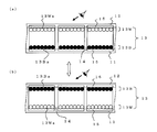
- FIG. 1A shows a case of white display
- FIG. 1B shows a case of black display.
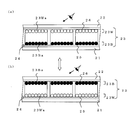
- FIG. 2A shows a case of white display
- FIG. 2B shows a case of black display.
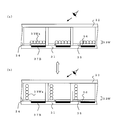
- FIG. 3A shows the case of white display
- FIG. 3B shows the case of black display.
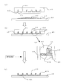
- FIG. 3A shows sequentially an example of the partition formation process by the imprint method of the information display panel of this invention.
- the basic configuration of the information display panel of the present invention will be described.
- this information display panel at least one kind of particles having optical reflectivity and chargeability (electric field driving) are formed in a space formed by cells defined by a partition wall between two opposing substrates, at least one of which is transparent.
- a display medium composed of possible particles) is enclosed.
- the charged display medium is attracted by the electric field force or Coulomb force along the applied electric field direction.
- information such as an image is displayed by moving the display medium according to the change in the electric field direction. Therefore, it is necessary to design the information display panel so that the display medium can be moved uniformly and the stability can be maintained when the display is rewritten repeatedly or when the display information is continuously displayed.
- the force applied to the particles constituting the display medium in addition to the force attracting each other by the Coulomb force between the particles, the electric mirror image force with the electrode and the substrate, the intermolecular force, the liquid cross-linking force, gravity and the like can be considered.
- FIGS. 1A and 1B are schematic cross-sectional views for explaining an example of the information display panel of the present invention.
- a white display medium 13 ⁇ / b> W composed of a group of white particles for display 13 ⁇ / b> Wa and a group of particles of a black particle for display 13 ⁇ / b> Ba
- a black display medium 13B is enclosed in each cell defined by the partition walls 14. Then, according to the electric field generated by applying a voltage between the electrode 15 (individual electrode) embedded in the substrate 11 and the electrode 16 (individual electrode) embedded in the substrate 12, the space between the substrate 11 and the substrate 12 is changed. Move vertically.
- the white display medium 13W is visually recognized by the observer (in the direction of the arrow) as shown in FIG. 1A, and white dot display is performed, or the black display medium 13B as shown in FIG. 1B.
- the black dots are displayed by visually recognizing.
- the electrodes are not limited to being embedded in the substrate, but may be provided on the substrate.
- a display unit (1 dot) is configured by providing a pair of individual electrodes opposed to each cell defined by a partition wall.
- FIG. 2A and 2B are schematic cross-sectional views for explaining another example of the information display panel of the present invention.
- display media 23 here, particle groups of white particles for display 23Wa
- produces by applying a voltage between the electrode 25 (line electrode) provided in the board
- the white display medium 23W is visually recognized by the observer (in the direction of the arrow) as shown in FIG. 2A, and white dot display is performed, or the black display medium 23B is displayed as shown in FIG.
- the black dots are displayed by visually recognizing.
- the electrode may be provided on the substrate outside the cell, or may be provided so as to be embedded in the substrate as shown in FIG. *
- a display unit (1 dot) is configured by associating a cell defined by a partition with a line electrode pair facing each other.
- FIG. 3A and 3B are schematic cross-sectional views for explaining another example of the information display panel of the present invention.
- a display medium 33 composed of particle groups of particles having optical reflectivity and chargeability here, a white display medium 33 ⁇ / b> W composed of particle groups of display white particles 33 ⁇ / b> Wa
- the white display medium 33W is visually recognized by the observer (in the direction of the arrow) to display white dots, or as shown in FIG. 3B, the color of the black plate 37B.
- the black dot display is performed by making the viewer visually recognize the above.
- the display can be performed in the same manner by using the white display medium 33W as a black display medium and the black plate 37B as a white plate.
- the electrode may be provided outside the substrate or may be provided so as to be embedded inside the substrate.
- the cell defined by the partition is a display unit (1 dot).
- an arbitrary color filter (not shown) is provided for each cell on the observer side substrate of the information display panel in FIG. Color display can be performed by moving the medium 13W or the black display medium 13B.
- a red color filter (not shown), a green color filter (not shown), on the observer side substrate of three consecutive cells or three adjacent cells of the information display panel of FIG. And a blue color filter (not shown).
- a display unit is constituted by the three cells, and by adjusting the movement of the white display medium 13W or the black display medium 13B in each of the display units, multicolor display is possible.
- a feature of the present invention relates to a method for manufacturing an information display panel having the above-described configuration, in which partition walls are formed by an imprint method using a mold, and fine particles contributing to improvement in reflectance of the information display panel in the partition material Is that they are distributed.
- partition walls are formed by an imprint method using a mold, and fine particles contributing to improvement in reflectance of the information display panel in the partition material Is that they are distributed.
- the imprint method used in the present invention is a microfabrication technique for forming a minute structure by applying a transfer technique using a mold.
- the imprint method includes a thermal imprint method in which a mold is pressed against a heated thermoplastic resin to transfer a fine uneven pattern, and a pattern is formed by cooling, and a UV curable resin that is liquid at room temperature is applied to the substrate. Then, there is a UV imprint method in which a UV transmissive mold is pressed against a resin and irradiated with ultraviolet rays to cure the resin on the substrate and form a pattern.
- the UV imprint method can form a pattern at room temperature, it is preferable in that a distortion due to a difference in linear expansion coefficient between the substrate and the mold due to heat hardly occurs, and a highly accurate pattern can be formed.
- FIG. 4 is a schematic cross-sectional view for sequentially explaining an example of the formation process by the imprinting method and the partition wall of the information display panel of the present invention.
- the preparation state of each material is demonstrated with the figure of Fig.4 (a).
- a mold 40 used for forming a partition wall by an imprint method secures a cell-shaped space between two substrates and a mold recess 42 in a planar view for forming a partition wall on one substrate surface.
- a partition wall formation pattern region 41 made up of a mold convex portion 44 having a square shape in plan view is provided.
- a display surface side substrate 46 which is the viewing side and is transparent is disposed. Then, a predetermined amount of a liquid ultraviolet curable resin composition 48 is applied as a partition wall material to the surface corresponding to the information display area on the surface. Fine particles 50 having a refractive index different from that of the ultraviolet curable resin composition 48 are dispersed in the ultraviolet curable resin composition 48. Next, the partition formation pattern region 41 of the mold 40 is aligned, placed and pressed so as to face the application surface of the ultraviolet curable resin composition 48 on the display surface side substrate 46, and the display surface side substrate 46. A laminate of the ultraviolet curable resin composition 48 and the mold 40 is formed (see FIG. 4B).
- the ultraviolet curable resin composition 48 containing the fine particles 50 is formed not only on the partition wall but also on the mold protrusion between the mold protrusion 44 and the display surface side substrate 46. It exists in the part-substrate space 100.
- the ultraviolet curable resin composition 48 in the laminate is cured by irradiating with ultraviolet rays. Thereafter, the mold 40 is removed from the cured ultraviolet curable resin composition 48b, whereby predetermined partition walls are formed in the information display area on the surface of the display surface side substrate 46, and the mold convex portion-substrate space. In 100, a residual film 100b formed by dispersing the fine particles 50 in the cured ultraviolet curable resin composition 48b is formed (FIG. 5C).
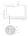
- FIG. 5A is a schematic plan view of the information display panel 60 having the partition walls formed as described above.
- this information display panel 60 two substrates 51 and 52 are bonded together, and an information display region 53 made up of an assembly of cell spaces defined by partition walls is formed between the substrates 51 and 52. .
- FIG. 5B the schematic plan view in which a part of the information display area 53 of the information display panel 60 is enlarged, the information display area 53 in which the fine particles 50 include the cell space 55 surface and the partition wall 54 portion. Since it is distributed over the entire surface, the reflectance of the information display panel can be effectively improved.
- the arrangement of the fine particles 50 is not limited to the end portion on the viewing side of the partition wall (see FIG. 4C), so that the change in reflectance due to the viewing angle of the information display panel is small and stable visibility improvement is achieved. An effect is obtained.
- a recess for forming a gap (substrate spacing) securing member for securing a gap between two substrates is further provided on the outer peripheral portion of the partition wall formation pattern region 41 of the mold 40.
- a gap securing member forming pattern region (not shown) may be provided. According to the gap securing member forming pattern region, the concern that the substrate is bent due to the pressure at the time of the pressure bonding of the two substrates, thereby causing the substrate spacing to be non-uniform is eliminated.
- the mold includes a metal or resin mold, a metal or resin stamper, and an intermediate stamper transferred from the mold to an IPS film (intermediate resin stamp film).
- a stamper or an intermediate stamper that can be used in the imprint method is preferable. Any material may be used, but preferably nickel, titanium, silicon, quartz, resin or the like can be applied.
- an ultraviolet transmissive mold is preferable, and an ultraviolet transmissive stamper or an intermediate stamper is particularly preferable.
- a stamper made of quartz or ultraviolet transmissive resin, and an intermediate stamper made of an ultraviolet transmissive resin film transferred from a metal stamper such as nickel by a thermal imprint method or the like are preferable.
- an ultraviolet curable resin composition is used as the partition wall material, but any ultraviolet curable resin composition may be used.
- a liquid ultraviolet curable resin composition that can be used in the imprint method is preferred.
- the liquid UV-curable resin composition preferably has a viscosity of 10 to 10,000 cps.
- the ultraviolet curable resin composition is preferably a composition containing an ultraviolet curable resin and a photoinitiator.
- ultraviolet curable resin examples include urethane acrylate, polyester acrylate, epoxy acrylate, epoxy resin, imide-based oligomer, and polyene / thiol-based oligomer.
- Urethane acrylates include, for example, diisocyanates such as hexamethylene diisocyanate, isophorone diisocyanate, methylene bis (4-cyclohexyl isocyanate), trimethylhexamethylene diisocyanate, tolylene diisocyanate, 4,4-diphenylmethane diisocyanate, xylylene diisocyanate, and poly (propylene oxide).
- diisocyanates such as hexamethylene diisocyanate, isophorone diisocyanate, methylene bis (4-cyclohexyl isocyanate), trimethylhexamethylene diisocyanate, tolylene diisocyanate, 4,4-diphenylmethane diisocyanate, xylylene diisocyanate, and poly (propylene oxide).
- Polyols such as diol, poly (propylene oxide) triol, poly (tetramethylene oxide) diol, ethoxylated bisphenol A and 2-hydroxyethyl acrylate 2-hydroxyethyl methacrylate, 2-hydroxypropyl acrylate, glycidol dimethacrylate, pentaerythritol tri Hydroxy acrylates such as acrylate Obtained by reacting, those having an acryloyl group and a urethane bond as a functional group in the molecule.
- polyester acrylate examples include polyester acrylate composed of phthalic anhydride, propylene oxide and acrylic acid, polyester acrylate composed of adipic acid, 1,6-hexanediol and acrylic acid, trimellitic acid, diethylene glycol and acrylic acid. And polyester acrylate.
- the epoxy acrylate is synthesized by reaction of an epoxy compound such as epichlorohydrin with acrylic acid or methacrylic acid.
- an epoxy compound such as epichlorohydrin with acrylic acid or methacrylic acid.
- bisphenol A type epoxy acrylate and bisphenol S synthesized by reaction of bisphenol A, epichlorohydrin and acrylic acid.
- Bisphenol S-type epoxy acrylate synthesized by reaction of chlorophenol, epichlorohydrin and acrylic acid bisphenol F-type epoxy acrylate synthesized by reaction of bisphenol F, epichlorohydrin and acrylic acid, synthesis by reaction of phenol novolac, epichlorohydrin and acrylic acid And phenol novolac type epoxy acrylate.
- epoxy resin examples include bisphenol type epoxy resins such as bisphenol A type epoxy resin, bisphenol F type epoxy resin, bisphenol AD type epoxy resin, and bisphenol S type epoxy resin; phenol novolac type epoxy resin, cresol novolak type epoxy resin and the like.
- examples include novolak-type epoxy resins; aromatic epoxy resins such as trisphenolmethane triglycidyl ether, and hydrogenated products and brominated products thereof.
- photopolymerization initiator a photoradical polymerization initiator and a photocationic polymerization initiator are preferable.
- the photoradical polymerization initiator include 4- (2-hydroxyethoxy) phenyl (2-hydroxy-2-propyl) ketone.
- Acetophenone derivatives such as ⁇ -hydroxy- ⁇ - ⁇ ′-dimethylacetophenone, methoxyacetophenone, 2,2-dimethoxy-2-phenylacetophenone; benzoin ether compounds such as benzoin ethyl ether and benzoin propyl ether; Ketal derivatives; halogenated ketones, acyl phosphine oxides, acyl phosphonates, 2-methyl-1- [4- (methylthio) phenyl] -2-morpholinopropan-1-one, 2-benzyl-2-N, N-dimethylamino-1 (4-morpholinophenyl) -1-butane, bis (2,4,6-trimethylbenzoyl) -phenylphosphine oxide bis- (2,6-dimethoxybenzoyl) 2,4,4-trimethylpentylphosphine oxide, Bis ( ⁇ 5-cyclopentadienyl) -bis (pentafluorophenyl) -
- photocationic polymerization initiator examples include iron-allene complex compounds, aromatic diazonium salts, aromatic iodonium salts, aromatic sulfonium salts, onium salts, pyridinium salts, aluminum complexes / silanol salts, trichloromethyltriazine derivatives, and the like. It is done.
- Examples of the counter anion of the onium salt or pyridinium salt include, for example, SbF6-, PF6-, AsF6-, BF4-, tetrakis (pentafluoro) borate, trifluoromethanesulfonate, methanesulfonate, trifluoroacetate, acetate, Examples thereof include sulfonate, tosylate, and nitrate.
- the addition amount of the photopolymerization initiator is generally 0.1 to 15 parts by mass, preferably 0.5 to 10 parts by mass with respect to 100 parts by mass of the ultraviolet curable resin.
- a reactive diluent may be added to the ultraviolet curable resin composition.
- the reactive diluent include 1,4-butanediol diacrylate, 1,6-hexanediol diacrylate, neopentyl.
- Glycol diacrylate 2- (2-ethoxyethoxy) ethyl acrylate, tetrahydrofurfuryl acrylate, 2-phenoxyethyl acrylate, diethylene glycol diacrylate, tetraethylene glycol diacrylate, 1,3-butylene glycol diacrylate, tripropylene glycol diacrylate , Trimethylolpropane triacrylate, pentaerythritol tetraacrylate, and hydroxypivalic acid neopentyl glycol diacrylate.
- the UV curable resin composition further includes photopolymerization initiation assistants, thermal polymerization inhibitors, fillers, adhesion-imparting agents, thixotropic agents, plasticizers, colorants, etc. that are generally added as necessary. May be added.
- the fine particles dispersed in the ultraviolet curable resin composition those having a refractive index different from that of the resin composition are used. This is because by changing the refractive index of the resin composition and the fine particles, scattering of external light in the remaining film and the partition can be promoted, and the reflectance of the entire information display area of the information display panel can be improved. .
- the refractive index (n p ) of the fine particles is expressed by the following formula (I):
- n p represents the refractive index of the fine particles and n r represents the refractive index of the resin composition.
- the refractive index of the fine particles is 1.20 to 2.30, preferably 1.30 to 1.65. If the refractive index of the fine particles is excessively large, the contrast of the panel is lowered, which is not preferable.
- the average particle size of the fine particles is 50 to 150, preferably 50 to 100. If it is too small, it is not economical as a fine particle material, and if it is too large, the film thickness of the remaining film is increased, which is not preferable in designing the information display panel.
- the content of the fine particles is preferably 10 to 60 parts by mass, particularly preferably 20 to 50 parts by mass with respect to 100 parts by mass of the resin composition. If there are too many fine particles in the resin composition, the remaining film is destroyed, so that it is impossible to obtain the effect of the present invention of increasing the reflectance of the information display panel more effectively and improving its visibility. . On the other hand, if the amount of fine particles is too small, the film thickness of the remaining film becomes non-uniform and the contrast of the information display panel is lowered, which is not preferable.
- the shape of the fine particles may be any shape, but is preferably a polyhedral shape, and particularly preferably a substantially spherical shape. This is because when the surface of the fine particles is increased, and further, the surface becomes substantially spherical, an efficient scattering effect of external light can be obtained.
- the material for the fine particles is not particularly limited, and examples thereof include organic substances such as resins, inorganic substances, compounds and mixtures thereof, and the like. However, since it is preferable that the refractive index is higher than that of the resin composition as the partition wall material, it is preferable to use inorganic fine particles having a high refractive index.
- silica (SiO 2 ), indium tin oxide (ITO), antimony oxide (III) (Sb 2 O 3 ), tin oxide (SnO 2 ), aluminum oxide (Al 2 O 3 ), titanium oxide (TiO 2 ), zirconium oxide (ZrO 2 ), and antimony tin oxide (ATO) can be mentioned, and silica (SiO 2 ), antimony (III) oxide (Sb 2 O 3 ), tin oxide ( SnO 2 ) and / or aluminum oxide (Al 2 O 3 ) can be used.
- the resin fine particles are preferably cross-linked in order to maintain a chemically stable state that does not dissolve in the liquid ultraviolet curable resin composition. These can be used alone or in combination of two or more.
- the ultraviolet curable resin composition when the imprint method is performed by the method shown in FIG. 4 described above, when the ultraviolet curable resin composition is cured, many light sources that emit ultraviolet light can be used as the light source, for example, ultra-high pressure, high pressure, low pressure Examples include mercury lamps, chemical lamps, xenon lamps, halogen lamps, mercury lamps, carbon arc lamps, incandescent lamps, and laser light.
- the irradiation time is not generally determined depending on the type of the lamp and the intensity of the light source, but is about 0.1 to several tens of seconds, preferably 0.5 to several seconds.
- the ultraviolet irradiation amount is preferably 300 mJ / cm 2 or more.
- the laminate may be preheated to 30 to 80 ° C. and irradiated with ultraviolet rays.
- At least one substrate is a transparent substrate from which the color of the display medium can be confirmed from the outside of the information display panel, and a material having high visible light transmittance and good heat resistance is suitable. is there.
- the back substrate may be transparent or opaque.
- substrate materials include polyethylene terephthalate (PET), polyethylene naphthalate (PEN), polyethersulfone (PES), polyethylene (PE), polycarbonate (PC), polyimide (PI), acrylic and other plastic substrates and glass A substrate is used.
- the thickness of the substrate is preferably 2 to 5000 ⁇ m, and more preferably 5 to 2000 ⁇ m. If it is too thin, it will be difficult to maintain the strength and uniformity of the distance between the substrates, and if it is thicker than 5000 ⁇ m, it will be a thin information display panel. Is inconvenient.
- metals such as aluminum, silver, nickel, copper, and gold, indium tin oxide (ITO), zinc-doped indium oxide (IZO), aluminum-doped zinc oxide (AZO), Conductive metal oxides such as indium oxide, conductive tin oxide, antimony tin oxide (ATO), and conductive zinc oxide, and conductive polymers such as polyaniline, polypyrrole, and polythiophene are exemplified and used as appropriate.
- ITO indium tin oxide
- IZO zinc-doped indium oxide
- AZO aluminum-doped zinc oxide
- Conductive metal oxides such as indium oxide, conductive tin oxide, antimony tin oxide (ATO), and conductive zinc oxide
- conductive polymers such as polyaniline, polypyrrole, and polythiophene are exemplified and used as appropriate.
- a method for forming the electrode a method of forming the above-described materials into a thin film by sputtering, vacuum vapor deposition, CVD (chemical vapor deposition), coating, or the like, or a method of laminating metal foil (for example, rolled copper foil) ) Or a method in which a conductive agent is mixed with a solvent or a synthetic resin binder and applied.
- An electrode (for example, 16 in FIG. 1) provided on the display-side substrate that needs to be transparent on the viewing side needs to be transparent, but an electrode provided on the back-side substrate (also 15 in FIG. 1). Need not be transparent.
- the above-mentioned material that can be patterned and is electrically conductive can be suitably used.
- the thickness of the electrode is preferably 0.01 to 10 ⁇ m, and preferably 0.05 to 5 ⁇ m, as long as the conductivity is ensured and the light transmittance is not affected.
- the material and thickness of the electrode provided on the back side substrate are the same as those of the electrode provided on the display surface side substrate described above, but need not be transparent. In this case, the external voltage input may be superimposed with direct current or alternating current.
- the height and width of the partition are appropriately set according to the type of the display medium involved in the display and are not limited in general, but the partition width is 2
- the height of the partition wall is adjusted to 10 to 500 ⁇ m, preferably 10 to 200 ⁇ m, more preferably 10 to 100 ⁇ m, and particularly preferably 10 to 50 ⁇ m.
- the height of the partition wall can be matched with the inter-substrate gap (substrate interval) or partially lower than the inter-substrate gap.
- the cells in the information display panel obtained by superimposing the display side substrate and the back side substrate are exemplified by polygons such as a square shape, a triangular shape, a line shape, a circular shape, and a hexagonal shape as viewed from the substrate plane direction.
- the shape may be any of a circular shape, an elliptical shape, a race track shape, or a combination of different shapes.
- the cell shape is preferably a polygon with rounded corners (especially a square with rounded corners), a circle, an ellipse, or a racetrack, because the display medium can easily move.
- Examples of the cell arrangement include a lattice shape, a honeycomb shape, and a mesh shape.
- Various shapes are used depending on the shape of the partition wall.
- a configuration in which square cells with rounded corners are arranged in a lattice shape is preferable, and a portion corresponding to a partition wall cross-sectional portion seen from the display surface side (the area of the cell frame formed by the partition wall width) is made as small as possible. This is preferable because the clearness of the display state is increased.
- the pattern shape is not particularly limited, and a conventionally known pattern shape can be used.
- a line shape, a bent shape, a dot shape, or the like, or a member with a small area connected in whole or in part, or a shape integrated with a partition wall of the information display area may be used.
- Display particles display particles (hereinafter also referred to as particles) constituting the particle group used as the display medium of the present invention will be described.
- the display particles can be used as a display medium by being composed of display particles alone, or by being combined with other particles as a display medium.
- the particles can contain a charge control agent, a colorant, an inorganic additive, etc., if necessary, in the resin as the main component, if necessary.
- a charge control agent e.g., a colorant, an inorganic additive, etc.
- resins, charge control agents, colorants, and other additives will be given below.
- the resin examples include urethane resin, urea resin, acrylic resin, polyester resin, acrylic urethane resin, acrylic urethane silicone resin, acrylic urethane fluororesin, acrylic fluororesin, silicone resin, acrylic silicone resin, epoxy resin, polystyrene resin, styrene Acrylic resin, polyolefin resin, butyral resin, vinylidene chloride resin, melamine resin, phenol resin, fluororesin, polycarbonate resin, polysulfone resin, polyether resin, polyamide resin and the like can be mentioned, and two or more kinds can be mixed.
- acrylic urethane resin, acrylic silicone resin, acrylic fluororesin, acrylic urethane silicone resin, acrylic urethane fluororesin, fluororesin, and silicone resin are suitable from the viewpoint of controlling the adhesive force with the substrate.
- the charge control agent is not particularly limited.
- the negative charge control agent include salicylic acid metal complexes, metal-containing azo dyes, metal-containing oil-soluble dyes (including metal ions and metal atoms), and quaternary ammonium salt systems. Examples thereof include compounds, calixarene compounds, boron-containing compounds (benzyl acid boron complexes), and nitroimidazole derivatives.
- the positive charge control agent include nigrosine dyes, triphenylmethane compounds, quaternary ammonium salt compounds, polyamine resins, imidazole derivatives, and the like.
- metal oxides such as ultrafine silica, ultrafine titanium oxide, ultrafine alumina, nitrogen-containing cyclic compounds such as pyridine and derivatives and salts thereof, various organic pigments, resins containing fluorine, chlorine, nitrogen, etc. are also charged. It can also be used as a control agent.
- colorant various organic and inorganic pigments and dyes can be used.
- black colorants examples include carbon black, copper oxide, manganese dioxide, aniline black, activated carbon and the like.
- blue colorants include C.I. I. Pigment blue 15: 3, C.I. I. Pigment Blue 15, Bituminous Blue, Cobalt Blue, Alkaline Blue Lake, Victoria Blue Lake, Phthalocyanine Blue, Metal-free Phthalocyanine Blue, Partially Chlorinated Phthalocyanine Blue, Fast Sky Blue, Indanthrene Blue BC and the like.
- red colorants examples include bengara, cadmium red, red lead, mercury sulfide, cadmium, permanent red 4R, resol red, pyrazolone red, watching red, calcium salt, lake red D, brilliant carmine 6B, eosin lake, rhodamine lake.
- B Alizarin Lake, Brilliant Carmine 3B, C.I. I. Pigment Red 2 etc.
- yellow colorants include chrome yellow, zinc yellow, cadmium yellow, yellow iron oxide, mineral first yellow, nickel titanium yellow, navel yellow, naphthol yellow S, Hansa Yellow G, Hansa Yellow 10G, Benzidine Yellow G, Benzidine Yellow GR, Quinoline Yellow Lake, Permanent Yellow NCG, Tartrazine Lake, C.I. I. Pigment yellow 12 and the like.
- green colorants include chrome green, chromium oxide, pigment green B, C.I. I. Pigment Green 7, Malachite Green Lake, Final Yellow Green G and the like.
- orange colorants examples include red chrome yellow, molybdenum orange, permanent orange GTR, pyrazolone orange, vulcan orange, indanthrene brilliant orange RK, benzidine orange G, indanthrene brilliant orange GK, C.I. I. And CI Pigment Orange 31.
- purple colorants examples include manganese purple, first violet B, and methyl violet lake.
- white colorants include zinc white, titanium oxide, antimony white, and zinc sulfide.
- extender pigments examples include barite powder, barium carbonate, clay, silica, white carbon, talc, and alumina white.
- various dyes such as basic, acidic, dispersion, and direct dyes include nigrosine, methylene blue, rose bengal, quinoline yellow, and ultramarine blue.
- inorganic additives include titanium oxide, zinc white, zinc sulfide, antimony oxide, calcium carbonate, lead white, talc, silica, calcium silicate, alumina white, cadmium yellow, cadmium red, cadmium orange, titanium yellow,
- pigments and inorganic additives can be used alone or in combination.
- carbon black can be preferably used as the black pigment
- titanium oxide can be preferably used as the white pigment.
- the above colorant can be blended to produce display particles of a desired color.
- the display particles of the present invention preferably have an average particle diameter d (0.5) in the range of 1 to 20 ⁇ m and are uniform and uniform. If the average particle diameter d (0.5) is larger than this range, the display is not clear. If the average particle diameter d (0.5) is smaller than this range, the cohesive force between particles becomes too large, which may hinder movement as a display medium. is there.
- the particle size distribution Span represented by the following formula is less than 5, preferably less than 3.
- Span (d (0.9) ⁇ d (0.1)) / d (0.5) (However, d (0.5) is a numerical value expressed in ⁇ m that the particle diameter is 50% larger than this and 50% smaller than this, and d (0.1) is the ratio of particles smaller than 10%. % Is a numerical value expressing the particle diameter in ⁇ m, and d (0.9) is a numerical value expressing the particle diameter in which 90% or less of the particles are less than this in ⁇ m.)
- the size of each particle is uniform, and uniform movement as a display medium becomes possible.
- the ratio of d (0.5) of particles having the smallest diameter to d (0.5) of particles having the largest diameter among the display particles used is 10 or less. Even if the particle size distribution Span is reduced, particles with different charging characteristics move in opposite directions, so that the particle size is close to each other and each particle can be easily moved in the opposite direction by the equivalent amount. This is within this range.
- the particle size distribution and particle size of the display particles can be obtained from a laser diffraction / scattering method or the like.
- a light intensity distribution pattern of diffracted / scattered light is spatially generated, and this light intensity pattern has a corresponding relationship with the particle diameter, so that the particle diameter and particle diameter distribution can be measured.
- the particle size and particle size distribution in the present invention are obtained from a volume-based distribution. Specifically, using a Mastersizer 2000 particle size distribution measuring device (Malvern), put the particles in a nitrogen stream and use the attached analysis software (software based on volume reference distribution using Mie theory). Thus, the particle size and particle size distribution can be measured.
- a Mastersizer 2000 particle size distribution measuring device Malvern
- put the particles in a nitrogen stream and use the attached analysis software software based on volume reference distribution using Mie theory.
- the charge amount of the display particles naturally depends on the measurement conditions, but the charge amount of the display particles in the information display panel is almost the initial charge amount, the contact with the partition wall, the contact with the substrate, and the charge decay with the elapsed time.
- the saturation value of the charging behavior of the display particles is a dominant factor. For example, by measuring the charge amount of the display particles using the same carrier particles in the blow-off method, it is possible to evaluate the range of the proper charge characteristic value of the display particles.
- the information display panel according to the present invention is a charged particle movement type information display panel for driving a display medium configured as a group of particles containing chargeable particles in a gas space
- a void portion surrounding the display medium Gas management is important and contributes to improved display stability. Specifically, it is important that the relative humidity at 25 ° C. is 60% RH or less, preferably 50% RH or less with respect to the humidity of the gas in the void portion.
- the void portion excludes the occupied portion of the display medium 13, the occupied portion of the partition wall 14, and the seal portion of the information display panel from the portion sandwiched between the opposing substrates 11 and 12.
- a gas portion in contact with a so-called display medium is indicated.
- the gas in the gap is not limited as long as it is in the humidity region described above, but dry air, dry nitrogen, dry argon, dry helium, dry carbon dioxide, dry methane and the like are suitable.
- This gas must be sealed in the information display panel so that the humidity is maintained. For example, filling of particles constituting the display medium, assembly of the information display panel, etc. are performed in a predetermined humidity environment.
- the distance between the substrates in the information display panel of the present invention is not limited as long as the display medium can be moved and the contrast can be maintained, but is usually 10 to 500 ⁇ m, preferably 10 to 200 ⁇ m, more preferably 10 to 100 ⁇ m, and particularly preferably. Is adjusted to 10 to 50 ⁇ m.
- the volume occupancy of the display medium in the gas space between the opposing substrates is preferably 5 to 70%, more preferably 5 to 60%. When it exceeds 70%, the movement as a display medium is hindered, and when it is less than 5%, the contrast tends to be unclear.
- the driving method of the information display panel of the present invention a simple matrix driving method and a static driving method that do not use a switching element in the panel itself, a three-terminal switching element represented by a thin film transistor (TFT), or a thin film diode (TFD).
- TFT thin film transistor
- TFD thin film diode
- Various types of driving systems such as an active matrix driving system using a two-terminal switching element represented by the above can be applied.
- the present invention also provides an information display panel manufactured by the information display panel manufacturing method of the present invention described above.
- the partition walls which are characteristic features thereof are as described in [Partition formation step and partition wall] regarding the method for manufacturing the information display panel of the present invention.
- the information display panel of the present invention is manufactured using the manufacturing method of the present invention, the visibility is further improved as compared with the prior art without reducing the productivity.
- Example 1 Preparation of information display panel (1) Preparation of UV curable resin composition in which fine particles contributing to improvement in reflectivity of information display panel are dispersed. Materials are mixed according to the formulation shown in Table 1, and UV curable resin composition is prepared. I adjusted things. The dispersed fine particles are TiO 2 (particle size 250 nm, refractive index 2.3). (2) Formation of partition wall By applying the ultraviolet curable resin composition prepared in (1) to the surface corresponding to the information display area on the display surface side substrate, and placing and pressing the mold from above, A laminate of the display surface side substrate, the ultraviolet curable resin composition, and the mold was formed. The laminate was irradiated with ultraviolet rays to cure the ultraviolet curable resin composition, and then the mold was removed to form partition walls in the information display area on the surface of the display surface side substrate.
- an information display panel was prepared according to a conventionally known method.
- Example 2 An information display panel was produced in the same manner as in Example 1 except that the fine particles of Example 1 (1) were changed to TiO 2 (particle diameter 160 nm, refractive index 2.3).
- Example 3 An information display panel was produced in the same manner as in Example 1 except that the fine particles of Example 1 (1) were changed to TiO 2 (particle diameter 90 nm, refractive index 2.3).
- Example 4 An information display panel was produced in the same manner as in Example 1 except that the fine particles of Example 1 (1) were changed to CeO 2 (particle diameter 80 nm, refractive index 2.2).
- Example 5 An information display panel was produced in the same manner as in Example 1 except that the fine particles of Example 1 (1) were changed to ZnO (particle diameter 80 nm, refractive index 2.1).
- Example 6 An information display panel was produced in the same manner as in Example 1 except that the fine particles of Example 1 (1) were SnO 2 (particle diameter 60 nm, refractive index 1.95).
- Example 7 An information display panel was produced in the same manner as in Example 1 except that the fine particles of Example 1 (1) were Al 2 O 3 (particle diameter 80 nm, refractive index 1.63).
- Example 8 An information display panel was produced in the same manner as in Example 1 except that the fine particles of Example 1 (1) were changed to SiO 2 (particle diameter 100 nm, refractive index 1.46).
- Example 9 An information display panel was produced in the same manner as in Example 1 except that the fine particles of Example 1 (1) were changed to SiO 2 (particle diameter 80 nm, refractive index 1.3).
- Example 1 An information display panel was produced in the same manner as in Example 1 except that the fine particles of Example 1 (1) were not added.
- the refractive index of the ultraviolet curable resin composition not containing fine particles was 1.5.
- the brightness of the information display panel was measured by using a spectrophotometric luminance meter U-4000 by a method of obtaining the visibility reflectance from the diffuse reflectance in a 20-degree ring.
- the transmittance decreases and the brightness decreases, that is, the difference between the black display and the white display of the panel decreases.
- the evaluation of brightness the case where the panel reflectivity is smaller than 20% is evaluated as ⁇ , and the case where it is larger than 20% is evaluated as ⁇ .
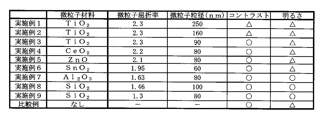
- Table 2 below shows evaluations regarding contrast and brightness of the information display panels produced in Examples 1 to 9 and Comparative Examples.
- an information display panel of the present invention it is possible to manufacture an information display panel in which corrosion or the like of electrodes in the input power unit is prevented with high productivity. Therefore, according to the present invention, a notebook computer, an electronic notebook, a portable information device called PDA (Personal Digital Assistants), a display unit of a mobile device such as a mobile phone, a handy terminal, an electronic book, an electronic newspaper, an electronic manual (instruction manual), etc.
- PDA Personal Digital Assistants
- Electronic paper Electronic paper, electronic signage (digital signage), posters, bulletin boards such as blackboards (whiteboards), display units for electronic desk calculators, home appliances, automobiles, card displays such as point cards and IC cards, electronic advertisements, Information boards, electronic POPs (Point Of Presence, Point Of Purchase advertising), electronic price tags, electronic shelf labels, electronic musical scores, RF-ID device display units, POS terminals, car navigation devices, display units for various electronic devices such as watches , And rewritable paper that can be rewritten on a rewriting device with high quality and low cost Can be manufactured.
Landscapes
- Physics & Mathematics (AREA)
- Nonlinear Science (AREA)
- Health & Medical Sciences (AREA)
- Life Sciences & Earth Sciences (AREA)
- Chemical & Material Sciences (AREA)
- Chemical Kinetics & Catalysis (AREA)
- Electrochemistry (AREA)
- Molecular Biology (AREA)
- General Physics & Mathematics (AREA)
- Optics & Photonics (AREA)
- Devices For Indicating Variable Information By Combining Individual Elements (AREA)
- Electrochromic Elements, Electrophoresis, Or Variable Reflection Or Absorption Elements (AREA)
Abstract
従来の情報表示用パネルより、視認性をさらに向上させた情報表示用パネルを、生産性を低下させずに製造する方法を提供する。 少なくとも一方が透明な対向する2枚の基板の一方の基板の表面に、金型40を用いるインプリント法により隔壁を形成して、その基板間に当該隔壁により画成された多数のセルからなる空間を設け、それぞれの空間に帯電性を有する多数の粒子から構成される表示媒体を封入することにより、電界の付与によって前記表示媒体を移動させて情報を表示する情報表示用パネルを製造する方法であって、前記隔壁を形成する隔壁材料が、微粒子50を含む樹脂組成物48からなり、且つ当該微粒子の屈折率が、前記樹脂組成物の基材樹脂の屈折率と異なることを特徴とする情報表示用パネルの製造方法。
Description
本発明は、少なくとも一方が透明な対向する2枚の基板間の空間に、電界駆動可能な表示媒体を封入し、基板内に発生させた電界により表示媒体を移動させて画像等の情報を表示する情報表示用パネルの製造方法及び情報表示用パネルに関するものである。
液晶表示装置(LCD)に代わる情報表示装置として、帯電粒子を液体中で駆動させる方式(電気泳動方式)の情報表示装置や、帯電粒子を気体中で駆動させる方式(例えば、電子粉流体方式)の情報表示装置が知られている。
後者の帯電粒子駆動方式の情報表示装置に用いる情報表示用パネルは、少なくとも一方が透明な対向する2枚の基板間の空間に、少なくとも一種類以上の粒子から構成される光学的反射率及び帯電性を有する電界駆動可能な表示媒体を封入し、基板に設けた電極から表示媒体に電界を付与することによって、表示媒体を移動させて画像等の情報を書き換え可能に表示する方式の情報表示用パネルが知られている(特許文献1)。
この情報表示用パネルにおいて、2枚の基板間の空間からなる情報表示領域は、基板平行方向の余分な粒子移動を阻止し、耐久繰り返し性、メモリ補助性を介助し、かつ基板間の間隔を均一にして画像表示板の強度を上げるために、隔壁により互いに隔離されたセル空間の集合体として構成されることが好ましい。
ここで、特許文献1のような情報表示装置は、一般的な液晶表示装置(LCD)のようにバックライト等の光源を有する自発光ディスプレイと異なり、外光の反射により情報を表示させる反射型ディスプレイである。従って、特許文献1のような情報表示装置は、一般的な液晶表示装置(LCD)と比較すると光量が少なく、表示画面が暗い。
特許文献2には、反射型ディスプレイ方式を採用する特許文献1のような情報表示用パネルにおいて、上述の隔壁の表示面側端部に反射性部材(ホワイトマトリックス)を取り付けてセル内の反射率を上げてパネル自体の反射率を向上させ、表示画面を全体的に明るくする技術が開示されている。
しかし、特許文献2に記載の技術では、表示画面を明るくするための反射性部材(ホワイトマトリックス)の設置は、隔壁の端部のみに限られている。そのため、観察角度による情報表示用パネルの白色反射率の変化があり、また隔壁の端部というように反射性部材(ホワイトマトリックス)の配置が限定的であるために、十分な視認性が得られない場合がある。さらに、反射性部材(ホワイトマトリックス)と隔壁は別の層となっているため、隔壁とは別に反射性部材(ホワイトマトリックス)を形成する必要があり、情報表示用パネルの製造工程が煩雑になりその生産性が低下する。
従って、本発明の目的は、従来の情報表示用パネルより視認性をさらに向上させた情報表示用パネルを、生産性を低下させずに製造する方法を提供することにある。また、本発明の目的は、この製造方法により製造された情報表示用パネルを提供することにある。
上記目的は、少なくとも一方が透明な対向する2枚の基板の一方の基板の表面に、インプリント法により隔壁を形成して、その基板間に当該隔壁により画成された多数のセルからなる空間を設け、それぞれの空間に帯電性を有する多数の粒子から構成される表示媒体を封入することにより、電界の付与によって前記表示媒体を移動させて情報を表示する情報表示用パネルを製造する方法であって、前記隔壁を形成する隔壁材料が、微粒子を含む樹脂組成物からなり、且つ当該微粒子の屈折率が、前記樹脂組成物の基材樹脂の屈折率と異なることを特徴とする情報表示用パネルの製造方法によって達成される。
このように基材樹脂の屈折率と異なる屈折率を有する微粒子を分散させることにより隔壁材料中の基材樹脂と微粒子の境界面で外光が散乱して、情報表示用パネルの反射率が大きくなる。
そして、微粒子は、隔壁端部に限らず、隔壁全体、及びインプリント法によりセル空間と基板の間に生じる残膜部分に分散可能なので、この隔壁全体および残膜部分における外光の散乱により情報表示用パネル全体の反射率を効果的に高めて、その視認性を向上させることができる。さらに、これは隔壁材料に、その基材樹脂と屈折率が異なる微粒子を分散させるという簡易な操作で達成可能であるため、反射部材を隔壁端部に積層するといった追加工程も必要なく、情報表示用パネルの生産性を低下させることがない。
本発明の情報表示用パネルの製造方法の好ましい態様は以下の通りである。
(1)前記微粒子の屈折率(np)が、下記式(I):

(2)前記微粒子が、無機微粒子である。
(3)前記微粒子の屈折率が、1.20~2.30である。
(4)前記微粒子の平均粒径が、50~150である。
(5)前記無機微粒子が、シリカ(SiO2)、酸化アンチモン(III)(Sb2O3)、酸化錫(SnO2)、及び酸化アルミニウム(Al2O3)からなる群から選択される少なくとも1種である。
(6)前記樹脂組成物が、紫外線硬化性樹脂組成物である。
また、上記目的は、本発明の情報表示用パネルの製造方法によって製造されたことを特徴とする情報表示用パネルによっても達成される。
本発明の方法によれば、隔壁端部に限らず、隔壁全体、及びインプリント法によりセル空間と基板の間に生じる残膜部分における外光の散乱を効果的に高めることができる。従って、より効果的に情報表示用パネルの反射率を高めて、その視認性を向上させることができる。さらに、これは隔壁材料に、その基材樹脂と屈折率が異なる微粒子を分散させるという簡易な操作で達成可能であるため、反射部材を隔壁端部に積層するといった追加工程も必要なく、情報表示用パネルの生産性を低下させることがない。
本発明の実施の形態について、図面を参照しながら説明する。
まず、本発明の情報表示用パネルの基本的な構成について説明する。この情報表示用パネルでは、少なくとも一方が透明な対向する2枚の基板間の隔壁により画成されたセルからなる空間に、少なくとも1種類以上の光学的反射率と帯電性を有する粒子(電界駆動可能な粒子ともいう)から構成される表示媒体が封入されている。その表示媒体に電界を付与することにより、付与された電界方向に沿って、帯電した表示媒体が電界による力やクーロン力などによって引き寄せられる。そして、電界方向の変化によって表示媒体が移動することにより、画像等の情報表示がなされる。従って、表示媒体が均一に移動し、且つ繰り返し表示を書き換えるとき、あるいは表示情報を継続して表示するときの安定性を維持できるように、情報表示用パネルを設計する必要がある。ここで、表示媒体を構成する粒子にかかる力は、粒子同士のクーロン力により引きつけ合う力の他に、電極や基板との電気鏡像力、分子間力、液架橋力、重力などが考えられる。
本発明のドットマトリックス型情報表示用パネルの例を、図1~3に基づいて説明する。
図1(a)、(b)は、本発明の情報表示用パネルの一例を説明するための概略断面図である。図1においては、光学的反射率および帯電性が異なる少なくとも2種以上の表示媒体13(ここでは表示用白色粒子13Waの粒子群からなる白色表示媒体13Wと表示用黒色粒子13Baの粒子群からなる黒色表示媒体13Bを示す)を、隔壁14で画成された各セルに封入している。そして、基板11に埋設した電極15(個別電極)と基板12に埋設した電極16(個別電極)との間に電圧を印加することにより発生する電界に応じて、基板11と基板12の間を垂直に移動させる。これにより、図1(a)に示すように白色表示媒体13Wを観察者(矢印方向)に視認させて白色ドット表示を行い、又は図1(b)に示すように黒色表示媒体13Bを観察者に視認させて黒色ドット表示を行っている。電極は基板に埋設する形態に限らず、基板上に設けても良い。図1においては、隔壁によって画成されるセルごとに対向する一対の個別電極対を設けることにより表示単位(1ドット)を構成している。
図2(a)、(b)は、本発明の情報表示用パネルの別の一例を説明するための概略断面図である。図2においては、光学的反射率および帯電性を有する粒子の粒子群から構成される光学的反射率および帯電特性が異なる少なくとも2種以上の表示媒体23(ここでは表示用白色粒子23Waの粒子群からなる白色表示媒体23Wと表示用黒色粒子23Baの粒子群からなる黒色表示媒体23Bを示す)が、隔壁24で画成された各セルに封入されている。そして、基板21に設けた電極25(ライン電極)と基板22に設けた電極26(ライン電極)との間に電圧を印加することにより発生する電界に応じて、基板21と基板22の間を垂直に移動させる。これにより、図2(a)に示すように白色表示媒体23Wを観察者(矢印方向)に視認させて白色ドット表示を行い、又は図2(b)に示すように黒色表示媒体23Bを観察者に視認させて黒色ドット表示を行っている。電極はセルの外側の基板上に設けても、図1のように基板の内部に埋め込むように設けても良い。
図2においては、隔壁によって画成されるセルと対向するライン電極対とを対応させて表示単位(1ドット)を構成している。
図3(a)、(b)は、本発明の情報表示用パネルの別の一例を説明するための概略断面図である。図3においては、光学的反射率および帯電性を有する粒子の粒子群から構成される表示媒体33(ここでは表示用白色粒子33Waの粒子群からなる白色表示媒体33Wを示す)を、隔壁34で画成された各セルに封入している。そして、基板31に設けた電極35と電極36との間に電圧を印加することにより発生する電界に応じて、基板31と基板32の間を平行方向に移動させる。これにより、図3(a)に示すように、白色表示媒体33Wを観察者(矢印方向)に視認させて白色ドット表示を行い、又は図3(b)に示すように、黒色板37Bの色を観察者に視認させて黒色ドット表示を行っている。
ここで、白色表示媒体33Wを黒色表示媒体とし、黒色板37Bを白色板としても同様に表示を行うことができる。電極は基板の外側に設けても、基板の内部に埋め込むように設けても良い。ここでは隔壁によって画成されるセルが表示単位(1ドット)となる。
また、本発明の情報表示用パネルのさらなる変形例として、図1の情報表示用パネルの観察者側の基板上にセル単位で任意のカラーフィルター(図示せず)を設け、その状態で白色表示媒体13W又は黒色表示媒体13Bを移動させることで、カラー表示を行うことができる。
更に、図1の情報表示用パネルの3個の連続するセル又は3個の隣接するセルの観察者側の基板上に、赤色カラーフィルター(図示せず)、緑色カラーフィルター(図示せず)、及び青色カラーフィルター(図示せず)をそれぞれ設ける。そして、その3個のセルで表示単位を構成し、この表示単位のそれぞれにおいて白色表示媒体13W又は黒色表示媒体13Bの移動を調節することで、多色カラー表示が可能となる。
本発明の特徴は、上述の構成の情報表示用パネルを製造する方法に関し、隔壁が金型を用いるインプリント法により形成され、その隔壁材料中に情報表示用パネルの反射率向上に寄与する微粒子が分散されていることにある。以下、本発明の情報表示用パネルの製造方法の隔壁形成工程を説明しながら本発明の特徴について詳述する。
[隔壁形成工程及び隔壁]
本発明において用いるインプリント法は、金型による転写技術を応用した微小な構造を形成するための微細加工技術である。
本発明において用いるインプリント法は、金型による転写技術を応用した微小な構造を形成するための微細加工技術である。
インプリント法には、加熱した熱可塑性樹脂に金型を押し付けて微細な凹凸パターンを転写し、冷却してパターンを形成する熱インプリント法と、基板上に室温で液状の紫外線硬化樹脂を塗布し、紫外線透過性の金型を樹脂に押し当て、紫外線を照射させることで基板上の樹脂を硬化させパターンを形成するUVインプリント法とがある。
本発明においては、UVインプリント法が、室温でパターン形成ができるため、熱による基板、モールド間の線膨張係数差による歪が発生しにくく、高精度のパターン形成ができる点で好ましい。
図4は本発明の情報表示用パネルの隔壁及びそのインプリント法による形成工程の一例を順に説明するための概略断面図である。図4(a)の図にて、各材料の準備状態について説明する。図示のように、インプリント法による隔壁形成に用いる金型40は、一方の基板表面上に隔壁を形成するための平面視格子状の金型凹部42及び2枚の基板間のセル空間を確保するための平面視正方形状の金型凸部44からなる隔壁形成パターン領域41を有する。この隔壁形成パターン領域41を有する金型40の転写面側の下方に、視認側であり透明である表示面側基板46を配置する。そして、その表面上の情報表示領域に相当する面に、隔壁材料として所定量の液状の紫外線硬化性樹脂組成物48を塗布する。紫外線硬化性樹脂組成物48中には、その紫外線硬化性樹脂組成物48と異なる屈折率を有する微粒子50が分散している。次に、金型40の隔壁形成パターン領域41を表示面側基板46上の紫外線硬化性樹脂組成物48の塗布面と向かい合うように位置合わせし、載置、押圧し、表示面側基板46と紫外線硬化性樹脂組成物48と、金型40との積層体を形成する(図4(b)参照)。この時、図4(d)に示すように、微粒子50を含む紫外線硬化性樹脂組成物48が、隔壁部分のみだけでなく金型凸部44と表示面側基板46との間の金型凸部-基板間空間100に存在することになる。
次に、上述の積層体中の紫外線硬化性樹脂組成物48を紫外線照射することにより硬化させる。その後、金型40を、硬化した紫外線硬化性樹脂組成物48bから除去することで、表示面側基板46の表面上の情報表示領域に所定の隔壁が形成され、金型凸部‐基板間空間100には、硬化した紫外線硬化性樹脂組成物48b中に微粒子50が分散されてできた残膜100bが形成される(図5(c))。
図5(a)は、このようにして形成された隔壁を有する情報表示用パネル60の概略平面図である。この情報表示用パネル60は、2枚の基板51、52が張り合わせわれ、その基板51、52の間に、隔壁により画成されたセル空間の集合体からなる情報表示領域53が構成されている。その情報表示用パネル60の情報表示領域53の一部を拡大した概略平面図(図5(b))に示されるように、微粒子50がセル空間55面、隔壁54部分を含む情報表示領域53面全体に分散されているため効果的に情報表示パネルの反射率を向上させることができる。同時に、微粒子50はその配置が隔壁の視認側端部に限定されていないため(図4(c)参照)、情報表示用パネルの観察角度による反射率の変化が少なく、安定的な視認性向上効果が得られる。
金型40の変形例として、金型40の隔壁形成パターン領域41のさらに外周部に、2枚の基板間の間隔を確保するためのギャップ(基板間隔)確保用部材を形成するための凹部を有するギャップ確保用部材形成パターン領域(図示せず)を設けてもよい。ギャップ確保用部材形成パターン領域によると、2枚の基板の加圧接合時の圧力により生じる基板の撓み、それにより基板間隔が不均一になる懸念が解消される。
[金型]
本発明において、金型は、金属製又は樹脂製モールド、金属製又は樹脂製スタンパ、及び金型からIPSフィルム(中間樹脂スタンプフィルム)に転写した中間スタンパ等を含む。特にインプリント法に使用できるスタンパ又は中間スタンパが好ましい。材質はどのようなものでも良いが、好ましくはニッケル、チタン、シリコン、石英、樹脂等が適用できる。特に、上述の図4に示した方法のように、紫外線硬化性樹脂組成物からなる樹脂材料を用いる場合は、紫外線透過性の金型が好ましく、特に紫外線透過性のスタンパ又は中間スタンパが好ましい。特に、石英や紫外線透過性の樹脂製のスタンパ、及びニッケル製等の金属製スタンパから熱インプリント法等により転写した紫外線透過性の樹脂フィルム製の中間スタンパが好ましい。
本発明において、金型は、金属製又は樹脂製モールド、金属製又は樹脂製スタンパ、及び金型からIPSフィルム(中間樹脂スタンプフィルム)に転写した中間スタンパ等を含む。特にインプリント法に使用できるスタンパ又は中間スタンパが好ましい。材質はどのようなものでも良いが、好ましくはニッケル、チタン、シリコン、石英、樹脂等が適用できる。特に、上述の図4に示した方法のように、紫外線硬化性樹脂組成物からなる樹脂材料を用いる場合は、紫外線透過性の金型が好ましく、特に紫外線透過性のスタンパ又は中間スタンパが好ましい。特に、石英や紫外線透過性の樹脂製のスタンパ、及びニッケル製等の金属製スタンパから熱インプリント法等により転写した紫外線透過性の樹脂フィルム製の中間スタンパが好ましい。
[紫外線硬化性樹脂組成物]
上述の図4に示した方法でインプリント法を行う場合、隔壁材料として紫外線硬化性樹脂組成物を用いるが、その紫外線硬化性樹脂組成物はどのようなものを用いても良い。特にインプリント法に使用できる液状の紫外線硬化性樹脂組成物が好ましい。液状の紫外線硬化性樹脂組成物は一般に、粘度は10~10000cpsが好ましい。
上述の図4に示した方法でインプリント法を行う場合、隔壁材料として紫外線硬化性樹脂組成物を用いるが、その紫外線硬化性樹脂組成物はどのようなものを用いても良い。特にインプリント法に使用できる液状の紫外線硬化性樹脂組成物が好ましい。液状の紫外線硬化性樹脂組成物は一般に、粘度は10~10000cpsが好ましい。
紫外線硬化性樹脂組成物は紫外線硬化性樹脂と光開始剤を含む組成物が好ましい。
紫外線硬化性樹脂としては、例えば、ウレタンアクリレート、ポリエステルアクリレート、エポキシアクリレート、エポキシ樹脂、イミド系オリゴマー、ポリエン・チオール系オリゴマー等が挙げられる。
ウレタンアクリレートは、例えば、ヘキサメチレンジイソシアネート、イソホロンジイソシアネート、メチレンビス(4-シクロヘキシルイソシアネート)、トリメチルヘキサメチレンジイソシアネート、トリレンジイソシアネート、4,4-ジフェニルメタンジイソシアネート、キシリレンジイソシアネート等のジイソシアネート類とポリ(プロピレンオキサイド)ジオール、ポリ(プロピレンオキサイド)トリオール、ポリ(テトラメチレンオキサイド)ジオール、エトキシ化ビスフェノールA等のポリオール類と2-ヒドロキシエチルアクリレート2-ヒドロキシエチルメタクリレート、2-ヒドロキシプロピルアクリレート、グリシドールジメタクリレート、ペンタエリスリトールトリアクリレート等のヒドロキシアクリレート類とを反応させることによって得られ、分子中に官能基としてアクリロイル基とウレタン結合を有するものである。
ポリエステルアクリレートとしては、例えば、無水フタル酸とプロピレンオキサイドとアクリル酸とからなるポリエステルアクリレート、アジピン酸と1,6-ヘキサンジオールとアクリル酸とからなるポリエステルアクリレート、トリメリット酸とジエチレングリコールとアクリル酸とからなるポリエステルアクリレート等が挙げられる。
エポキシアクリレートは、エピクロルヒドリン等のエポキシ化合物とアクリル酸又はメタクリル酸との反応により合成されたものであり、例えば、ビスフェノールAとエピクロルヒドリンとアクリル酸との反応により合成されるビスフェノールA型エポキシアクリレート、ビスフェノールSとエピクロルヒドリンとアクリル酸との反応により合成されるビスフェノールS型エポキシアクリレート、ビスフェノールFとエピクロルヒドリンとアクリル酸との反応により合成されるビスフェノールF型エポキシアクリレート、フェノールノボラックとエピクロルヒドリンとアクリル酸との反応により合成されるフェノールノボラック型エポキシアクリレート等が挙げられる。
エポキシ樹脂としては、例えば、ビスフェノールA型エポキシ樹脂、ビスフェノールF型エポキシ樹脂、ビスフェノールAD型エポキシ樹脂、ビスフェノールS型エポキシ樹脂等のビスフェノール型エポキシ樹脂;フェノールノボラック型エポキシ樹脂、クレゾールノボラック型エポキシ樹脂等のノボラック型エポキシ樹脂;トリスフェノールメタントリグリシジルエーテル等の芳香族エポキシ樹脂、及び、これらの水添化物や臭素化物等が挙げられる。
光重合開始剤としては、光ラジカル重合開始剤及び光カチオン重合開始剤が好ましく、光ラジカル重合開始剤としては、例えば、4-(2-ヒドロキシエトキシ)フェニル(2-ヒドロキシ-2-プロピル)ケトン、α-ヒドロキシ-α-α’-ジメチルアセトフェノン、メトキシアセトフェノン、2,2-ジメトキシ-2-フェニルアセトフェノン等のアセトフェノン誘導体;ベンゾインエチルエーテル、ベンゾインプロピルエーテル等のベンゾインエーテル系化合物;ベンジルジメチルケタール等のケタール誘導体;ハロゲン化ケトン、アシルフォスフィンオキシド、アシルフォスフォナート、2-メチル-1-[4-(メチルチオ)フェニル]-2-モルフォリノプロパン-1-オン、2-ベンジル-2-N,N-ジメチルアミノ-1-(4-モルフォリノフェニル)-1-ブタン、ビス(2,4,6-トリメチルベンゾイル)-フェニルフォスフィンオキシドビス-(2,6-ジメトキシベンゾイル)2,4,4-トリメチルペンチルフォスフィンオキシド、ビス(η5-シクロペンタジエニル)-ビス(ペンタフルオロフェニル)-チタニウム、ビス(η5-シクロペンタジエニル)-ビス[2,6-ジフルオロー3-(1H-ピリ-1-イル)フェニル]-チタニウム、アントラセン、ペリレン、コロネン、テトラセン、ベンズアントラセン、フェノチアジン、フラビン、アクリジン、ケトクマリン、チオキサントン誘導体、ベンゾフェノン、アセトフェノン、2-クロロチオキサンソン、2,4-ジメチルチオキサンソン、2,4-ジエチルチオキサンソン、2,4-ジイソプロピルチオキサンソン、イソプロピルチオキサンソン等が挙げられる。光カチオン重合開始剤としては、例えば、鉄-アレン錯体化合物、芳香族ジアゾニウム塩、芳香族ヨードニウム塩、芳香族スルホニウム塩、オニウム塩、ピリジニウム塩、アルミニウム錯体/シラノール塩、トリクロロメチルトリアジン誘導体等が挙げられる。上記オニウム塩やピリジニウム塩の対アニオンとしては、例えば、SbF6-、PF6-、AsF6-、BF4-、テトラキス(ペンタフルオロ)ボレート、トリフルオロメタンスルフォネート、メタンスルフォネート、トリフルオロアセテート、アセテート、スルフォネート、トシレート、ナイトレート等が挙げられる。
光重合開始剤の添加量は、一般に紫外線硬化性樹脂100質量部に対して、0.1~15質量部であり、好ましくは、0.5~10質量部である。
上記紫外線硬化性樹脂組成物には、反応性希釈剤が添加されてもよく、反応性希釈剤としては、例えば、1,4-ブタンジオールジアクリレート、1,6-ヘキサンジオールジアクリレート、ネオペンチルグリコールジアクリレート、2-(2-エトキシエトキシ)エチルアクリレート、テトラヒドロフルフリルアクリレート、2-フェノキシエチルアクリレート、ジエチレングリコールジアクリレート、テトラエチレングリコールジアクリレート、1,3-ブチレングリコールジアクリレート、トリプロピレングリコールジアクリレート、トリメチロールプロパントリアクリレート、ペンタエリスリトールテトラアクリレート、ヒドロキシピバリン酸ネオペンチルグリコールジアクリレート等が挙げられる。
上記紫外線硬化性樹脂組成物には、更に、必要に応じて、一般に添加されている光重合開始助剤、熱重合禁止剤、充填剤、接着付与剤、チクソ付与剤、可塑剤、着色剤等が添加されていても良い。
[微粒子]
上記紫外線硬化性樹脂組成物に分散される微粒子としては、その屈折率が樹脂組成物と異なるものを用いる。樹脂組成物と微粒子の屈折率を変えることにより、残膜及び隔壁における外光の散乱を促進することができ、情報表示用パネルの情報表示領域全体の反射率を向上させることができるからである。具体的には、微粒子の屈折率(np)は、下記式(I):
上記紫外線硬化性樹脂組成物に分散される微粒子としては、その屈折率が樹脂組成物と異なるものを用いる。樹脂組成物と微粒子の屈折率を変えることにより、残膜及び隔壁における外光の散乱を促進することができ、情報表示用パネルの情報表示領域全体の反射率を向上させることができるからである。具体的には、微粒子の屈折率(np)は、下記式(I):

さらに具体的には、その微粒子の屈折率は1.20~2.30、好ましくは1.30~1.65である。微粒子の屈折率が過剰に大きいと、逆にパネルのコントラストが低下するため、好ましくない。微粒子の平均粒径は50~150、好ましくは50~100である。小さすぎると微粒子材料として経済的ではなく、大きすぎると残膜の膜厚を大きくすることになり情報表示用パネルの設計上好ましくない。
また、微粒子の含有量は、樹脂組成物100質量部に対して、10~60質量部であることが好ましく、特に、20~50質量部であることが好ましい。樹脂組成物中に微粒子が多すぎると残膜が破壊されるので、より効果的に情報表示用パネルの反射率を高めて、その視認性を向上させるという本願発明の効果を得ることができなくなる。逆に微粒子が少なすぎると残膜の膜厚が不均一となり情報表示パネルのコントラストの低下を招き、好ましくない。
微粒子の形状は、どのような形状でもよいが、多面体状であることが好ましく、特に、略球状であることが好ましい。微粒子の面が多くなる、さらには略球状となることにより、効率良い外光の散乱効果が得られるからである。
微粒子の材料としては、特に限定されず、例えば、樹脂等の有機物、無機物、これらの化合物や混合物等が挙げられる。しかし、隔壁材料である樹脂組成物よりも屈折率が大きいことが好ましいことから、高屈折率を有する無機物の微粒子の使用が好ましい。そのような無機微粒子として、シリカ(SiO2)、酸化インジウム錫(ITO)、酸化アンチモン(III)(Sb2O3)、酸化錫(SnO2)、酸化アルミニウム(Al2O3)、酸化チタン(TiO2)、酸化ジルコニウム(ZrO2)、及びアンチモン錫酸化物(ATO)を挙げることができ、好ましくは、シリカ(SiO2)、酸化アンチモン(III)(Sb2O3)、酸化錫(SnO2)、及び/又は酸化アルミニウム(Al2O3)を用いることができる。また、隔壁材料である樹脂組成物と屈折率が異なる材料であればよいことから、樹脂等を素材とする微粒子を用いることもできる。この場合、液状の紫外線硬化性樹脂組成物中においても溶解しない、化学的に安定な状態を保つためにも、樹脂微粒子は架橋されていることが好ましい。これらは単独であるいは2種以上組み合わせて使用することができる。
上述の図4に示した方法でインプリント法を行う場合、紫外線硬化性樹脂組成物を硬化する場合は、光源として紫外領域光を発光する多くのものが採用でき、例えば超高圧、高圧、低圧水銀灯、ケミカルランプ、キセノンランプ、ハロゲンランプ、マーキュリーハロゲンランプ、カーボンアーク灯、白熱灯、レーザ光等が挙げられる。照射時間は、ランプの種類、光源の強さによって一概には決められないが、0.1秒~数十秒程度、好ましくは0.5~数秒である。紫外線照射量は、300mJ/cm2以上が好ましい。
また、硬化促進のために、予め積層体を30~80℃に加温し、これに紫外線を照射してもよい。
以下、本発明の情報表示用パネルを構成する各部材について説明する。
基板については、少なくとも一方の基板(表示面側基板)は情報表示用パネル外側から表示媒体の色が確認できる透明な基板であり、可視光の透過率が高くかつ耐熱性の良い材料が好適である。背面側基板は透明でも不透明でもかまわない。基板材料を例示すると、ポリエチレンテレフタレート(PET)、ポリエチレンナフタレート(PEN)、ポリエーテルサルフォン(PES)、ポリエチレン(PE)、ポリカーボネート(PC)、ポリイミド(PI)、アクリル等のプラスチック系基板やガラス基板を用いる。基板の厚みは、2~5000μmが好ましく、さらに5~2000μmが好適であり、薄すぎると、強度、基板間の間隔均一性を保ちにくくなり、5000μmより厚いと、薄型情報表示用パネルとする場合に不都合がある。
情報表示用パネルに設ける電極の形成材料としては、アルミニウム、銀、ニッケル、銅、金等の金属類や酸化インジウム錫(ITO)、亜鉛ドープ酸化インジウム(IZO)、アルミニウムドープ酸化亜鉛(AZO)、酸化インジウム、導電性酸化錫、アンチモン錫酸化物(ATO)、導電性酸化亜鉛等の導電金属酸化物類、ポリアニリン、ポリピロール、ポリチオフェンなどの導電性高分子類が例示され適宜選択して用いられる。電極の形成方法としては、上記例示の材料をスパッタリング法、真空蒸着法、CVD(化学蒸着)法、塗布法等で薄膜状に形成する方法や、金属箔をラミネートする方法(例えば、圧延銅箔)や、導電剤を溶媒や合成樹脂バインダーに混合して塗布したりする方法が用いられる。
視認側であり透明である必要のある表示面側基板に設ける電極(例えば、図1においては16)は透明である必要があるが、背面側基板に設ける電極(同じく、図1においては15)は透明である必要はない。いずれの場合もパターン形成可能で導電性である上記材料を好適に用いることができる。なお、電極の厚みは、導電性が確保でき光透過性に支障がなければ良く、0.01~10μm、好ましくは0.05~5μmが好適である。背面側基板に設ける電極の材質や厚みなどは上述した表示面側基板に設ける電極と同様であるが、透明である必要はない。なお、この場合の外部電圧入力は、直流あるいは交流を重畳しても良い。
情報表示用パネルの基板間の空間にセルを形成するための隔壁において、隔壁の高さや幅は表示にかかわる表示媒体の種類により適宜最適設定され、一概には限定されないが、隔壁の幅は2~100μm、好ましくは3~50μmに、隔壁の高さは10~500μm、好ましくは10~200μm、さらに好ましくは10~100μm、特に好ましくは10~50μmに調整される。隔壁の高さは基板間ギャップ(基板間隔)に合わせるか、部分的に基板間ギャップよりも低い高さとすることもできる。
表示側基板と背面側基板とを重ね合わせて得られる情報表示用パネルにおけるセルは、基板平面方向からみて四角状、三角状、ライン状、円形状、六角状等の多角形が例示されるが、円形、楕円形、レーストラック形などいずれでもよいし、異なる形状を組み合わせてもよい。セルの形状は表示媒体が移動しやすいものとして角丸付きの多角形(特には角丸付き四角形)、円形、楕円形、レーストラック形が好ましい。セルの配置の例としては格子状やハニカム状や網目状が挙げられる。隔壁形状によって様々な形状のものが用いられる。このうち、角丸付き四角形のセルを格子状に配置する構成が好ましく、表示面側から見える隔壁断面部分に相当する部分(隔壁の幅によって形成されるセルの枠部の面積)はできるだけ小さくした方が表示状態の鮮明さが増すので好ましい。
基板ギャップ確保用部材を設ける場合、通常、小面積の部材がパターン状に配置されたもので、パターン形状は特に制限は無く、従来公知のパターン形状を使用することができる。例えば、ライン形状、屈曲形状、ドット形状等、また、小面積の部材が全部又は部分的に連結したものでも良く、情報表示領域の隔壁と一体的な形状でも良い。
[表示用粒子]
次に、本発明の表示媒体とする粒子群を構成する表示用粒子(以下、粒子ともいう)について説明する。表示用粒子は、そのまま表示用粒子だけで構成して表示媒体としたり、その他の粒子と合わせて構成して表示媒体としたりして用いることができる。
次に、本発明の表示媒体とする粒子群を構成する表示用粒子(以下、粒子ともいう)について説明する。表示用粒子は、そのまま表示用粒子だけで構成して表示媒体としたり、その他の粒子と合わせて構成して表示媒体としたりして用いることができる。
粒子には、その主成分となる樹脂に、必要に応じて、従来と同様に、荷電制御剤、着色剤、無機添加剤等を含ますことができる。以下に、樹脂、荷電制御剤、着色剤、その他添加剤を例示する。
樹脂の例としては、ウレタン樹脂、ウレア樹脂、アクリル樹脂、ポリエステル樹脂、アクリルウレタン樹脂、アクリルウレタンシリコーン樹脂、アクリルウレタンフッ素樹脂、アクリルフッ素樹脂、シリコーン樹脂、アクリルシリコーン樹脂、エポキシ樹脂、ポリスチレン樹脂、スチレンアクリル樹脂、ポリオレフィン樹脂、ブチラール樹脂、塩化ビニリデン樹脂、メラミン樹脂、フェノール樹脂、フッ素樹脂、ポリカーボネート樹脂、ポリスルフォン樹脂、ポリエーテル樹脂、ポリアミド樹脂等が挙げられ、2種以上混合することもできる。特に、基板との付着力を制御する観点から、アクリルウレタン樹脂、アクリルシリコーン樹脂、アクリルフッ素樹脂、アクリルウレタンシリコーン樹脂、アクリルウレタンフッ素樹脂、フッ素樹脂、シリコーン樹脂が好適である。
荷電制御剤としては、特に制限はないが、負荷電制御剤としては例えば、サリチル酸金属錯体、含金属アゾ染料、含金属(金属イオンや金属原子を含む)の油溶性染料、4級アンモニウム塩系化合物、カリックスアレン化合物、含ホウ素化合物(ベンジル酸ホウ素錯体)、ニトロイミダゾール誘導体等が挙げられる。正荷電制御剤としては例えば、ニグロシン染料、トリフェニルメタン系化合物、4級アンモニウム塩系化合物、ポリアミン樹脂、イミダゾール誘導体等が挙げられる。その他、超微粒子シリカ、超微粒子酸化チタン、超微粒子アルミナ等の金属酸化物、ピリジン等の含窒素環状化合物及びその誘導体や塩、各種有機顔料、フッ素、塩素、窒素等を含んだ樹脂等も荷電制御剤として用いることもできる。
着色剤としては、有機または無機の各種、各色の顔料、染料が使用可能である。
黒色着色剤の例としては、カーボンブラック、酸化銅、二酸化マンガン、アニリンブラック、活性炭等が挙げられる。
青色着色剤の例としては、C.I.ピグメントブルー15:3、C.I.ピグメントブルー15、紺青、コバルトブルー、アルカリブルーレーキ、ビクトリアブルーレーキ、フタロシアニンブルー、無金属フタロシアニンブルー、フタロシアニンブルー部分塩素化物、ファーストスカイブルー、インダンスレンブルーBC等が挙げられる。
赤色着色剤の例としては、ベンガラ、カドミウムレッド、鉛丹、硫化水銀、カドミウム、パーマネントレッド4R、リソールレッド、ピラゾロンレッド、ウォッチングレッド、カルシウム塩、レーキレッドD、ブリリアントカーミン6B、エオシンレーキ、ローダミンレーキB、アリザリンレーキ、ブリリアントカーミン3B、C.I.ピグメントレッド2等がある。
黄色着色剤の例としては、黄鉛、亜鉛黄、カドミウムイエロー、黄色酸化鉄、ミネラルファーストイエロー、ニッケルチタンイエロー、ネーブルイエロー、ナフトールイエローS、ハンザイエローG、ハンザイエロー10G、ベンジジンイエローG、ベンジジンイエローGR、キノリンイエローレーキ、パーマネントイエローNCG、タートラジンレーキ、C.I.ピグメントイエロー12等が挙げられる。
緑色着色剤の例としては、クロムグリーン、酸化クロム、ピグメントグリーンB、C.I.ピグメントグリーン7、マラカイトグリーンレーキ、ファイナルイエローグリーンG等が挙げられる。
橙色着色剤の例としては、赤色黄鉛、モリブデンオレンジ、パーマネントオレンジGTR、ピラゾロンオレンジ、バルカンオレンジ、インダンスレンブリリアントオレンジRK、ベンジジンオレンジG、インダンスレンブリリアントオレンジGK、C.I.ピグメントオレンジ31等が挙げられる。
紫色着色剤の例としては、マンガン紫、ファーストバイオレットB、メチルバイオレットレーキ等が挙げられる。
白色着色剤の例としては、亜鉛華、酸化チタン、アンチモン白、硫化亜鉛等がある。
体質顔料の例としては、バライト粉、炭酸バリウム、クレー、シリカ、ホワイトカーボン、タルク、アルミナホワイト等が挙げられる。また、塩基性、酸性、分散、直接染料等の各種染料の例として、ニグロシン、メチレンブルー、ローズベンガル、キノリンイエロー、ウルトラマリンブルー等が挙げられる。
無機系添加剤の例としては、酸化チタン、亜鉛華、硫化亜鉛、酸化アンチモン、炭酸カルシウム、鉛白、タルク、シリカ、ケイ酸カルシウム、アルミナホワイト、カドミウムイエロー、カドミウムレッド、カドミウムオレンジ、チタンイエロー、紺青、群青、コバルトブルー、コバルトグリーン、コバルトバイオレット、酸化鉄、カーボンブラック、マンガンフェライトブラック、コバルトフェライトブラック、銅粉、アルミニウム粉などが挙げられる。
これらの顔料および無機系添加剤は、単独であるいは複数組み合わせて用いることができる。特に、黒色顔料としてカーボンブラック、白色顔料として酸化チタンを好ましく用いることができる。
上記着色剤を配合して所望の色の表示用粒子を作製できる。
また、本発明の表示用粒子は平均粒子径d(0.5)が、1~20μmの範囲であり、均一で揃っていることが好ましい。平均粒子径d(0.5)がこの範囲より大きいと表示上の鮮明さに欠け、この範囲より小さいと粒子同士の凝集力が大きくなりすぎるために表示媒体としての移動に支障をきたすおそれがある。
更に本発明の表示用粒子では、各粒子の粒子径分布に関して、下記式に示される粒子径分布Spanを5未満、好ましくは3未満とする。
Span=(d(0.9)-d(0.1))/d(0.5)
(但し、d(0.5)は粒子の50%がこれより大きく、50%がこれより小さいという粒子径をμmで表した数値、d(0.1)はこれ以下の粒子の比率が10%である粒子径をμmで表した数値、d(0.9)はこれ以下の粒子が90%である粒子径をμmで表した数値である。)
(但し、d(0.5)は粒子の50%がこれより大きく、50%がこれより小さいという粒子径をμmで表した数値、d(0.1)はこれ以下の粒子の比率が10%である粒子径をμmで表した数値、d(0.9)はこれ以下の粒子が90%である粒子径をμmで表した数値である。)
Spanを5以下の範囲に納めることにより、各粒子のサイズが揃い、表示媒体としての均一な移動が可能となる。
さらにまた、使用した表示用粒子の内、最大径を有する粒子のd(0.5)に対する最小径を有する粒子のd(0.5)の比を10以下とすることが重要である。たとえ粒子径分布Spanを小さくしたとしても、互いに帯電特性の異なる粒子が互いに反対方向に動くので、互いの粒子サイズが近く、互いの粒子が当量ずつ反対方向に容易に移動できるようにするのが好適であり、それがこの範囲となる。
なお、上記表示用粒子の粒子径分布および粒子径は、レーザー回折/散乱法などから求めることができる。測定対象となる粒子にレーザー光を照射すると空間的に回折/散乱光の光強度分布パターンが生じ、この光強度パターンは粒子径と対応関係があることから、粒子径および粒子径分布が測定できる。
ここで、本発明における粒子径および粒子径分布は、体積基準分布から得られたものである。具体的には、Mastersizer2000粒度分布測定装置(マルバーン社製)測定機を用いて、窒素気流中に粒子を投入し、付属の解析ソフト(Mie理論を用いた体積基準分布を基本としたソフト)にて、粒子径および粒子径分布の測定を行うことができる。
表示用粒子の帯電量は当然その測定条件に依存するが、情報表示用パネルにおける表示用粒子の帯電量はほぼ、初期帯電量、隔壁との接触、基板との接触、経過時間に伴う電荷減衰に依存し、特に表示用粒子の帯電挙動の飽和値が支配因子となっているということが分かっている。例えば、ブローオフ法において同一のキャリア粒子を用いて、表示用粒子の帯電量測定を行うことにより、表示用粒子の適正な帯電特性値の範囲を評価できる。
[その他]
更に、本発明の情報表示用パネルを、気体中空間で帯電性粒子を含んだ粒子群として構成した表示媒体を駆動する帯電粒子移動方式の情報表示用パネルとする場合、表示媒体を取り巻く空隙部分の気体の管理が重要であり、表示安定性向上に寄与する。具体的には、空隙部分の気体の湿度について、25℃における相対湿度を60%RH以下、好ましくは50%RH以下とすることが重要である。
更に、本発明の情報表示用パネルを、気体中空間で帯電性粒子を含んだ粒子群として構成した表示媒体を駆動する帯電粒子移動方式の情報表示用パネルとする場合、表示媒体を取り巻く空隙部分の気体の管理が重要であり、表示安定性向上に寄与する。具体的には、空隙部分の気体の湿度について、25℃における相対湿度を60%RH以下、好ましくは50%RH以下とすることが重要である。
この空隙部分とは、例えば図1(a)においては、対向する基板11と基板12に挟まれる部分から、表示媒体13の占有部分、隔壁14の占有部分、情報表示用パネルのシール部分を除いた、いわゆる表示媒体が接する気体部分を指すものとする。
空隙部分の気体は、先に述べた湿度領域であれば、その種類は問わないが、乾燥空気、乾燥窒素、乾燥アルゴン、乾燥ヘリウム、乾燥二酸化炭素、乾燥メタンなどが好適である。この気体は、その湿度が保持されるように情報表示用パネルに封入することが必要であり、例えば、表示媒体を構成する粒子の充填、情報表示用パネルの組み立てなどを所定湿度環境下にて行い、さらに、外からの湿度侵入を防ぐシール剤、シール方法を施すことが必要である。
本発明の情報表示用パネルにおける基板と基板との間隔は、表示媒体が移動できて、コントラストを維持できればよいが、通常10~500μm、好ましくは10~200μm、さらに好ましくは10~100μm、特に好ましくは10~50μmに調整される。
対向する基板間の気体中空間における表示媒体の体積占有率は5~70%が好ましく、さらに好ましくは5~60%である。70%を超える場合には表示媒体としての移動に支障をきたし、5%未満の場合にはコントラストが不明確となり易い。
本発明の情報表示用パネルの駆動方式については、パネル自体にスイッチング素子を用いない単純マトリックス駆動方式やスタティック駆動方式、また、薄膜トランジスタ(TFT)で代表される三端子スイッチング素子あるいは薄膜ダイオード(TFD)で代表される二端子スイッチング素子を用いたアクティブマトリックス駆動方式など、種々のタイプの駆動方式を適用することができる。
なお、本発明は上記の実施の形態の構成に限定されるものではなく、発明の要旨の範囲内で種々変形が可能である。
また、本発明は、上述の本発明の情報表示パネルの製造方法により製造された情報表示用パネルをも提供する。本発明の情報表示用パネルにおいて、その特徴的構成である隔壁については本発明の情報表示用パネルの製造方法に関する[隔壁形成工程及び隔壁]の記載の通りである。その他の構成については、上述の内容及び種々の従来公知の方法により提供可能である。本発明の情報表示用パネルは、本発明の製造方法を使用して製造されているので、生産性が低下せずにその視認性が従来技術よりもさらに向上した情報表示用パネルである。
以下、本発明を実施例により説明する。
[実施例1]
1.情報表示用パネルの作成
(1)情報表示用パネルの反射率向上に寄与する微粒子を分散させた紫外線硬化性樹脂組成物の調整
表1に記載の配合に従って材料を混合し、紫外線硬化性樹脂組成物を調整した。分散されている微粒子はTiO2(粒径250nm、屈折率2.3)である。
(2)隔壁の形成
(1)で調整した紫外線硬化性樹脂組成物を表示面側基板上の情報表示領域に相当する面に塗布し、その上から金型を載置、押圧することにより、表示面側基板と紫外線硬化性樹脂組成物と金型との積層体を形成した。この積層体に紫外線を照射し、紫外線硬化性樹脂組成物を硬化させたのちに金型を除去し、表示面側基板の表面上の情報表示領域に隔壁を形成した。
以降の工程については、従来公知の方法に従って情報表示用パネルを作成した。
[実施例2]
実施例1(1)の微粒子をTiO2(粒径160nm、屈折率2.3)とした以外は、実施例1と同様に情報表示用パネルを作製した。
実施例1(1)の微粒子をTiO2(粒径160nm、屈折率2.3)とした以外は、実施例1と同様に情報表示用パネルを作製した。
[実施例3]
実施例1(1)の微粒子をTiO2(粒径90nm、屈折率2.3)とした以外は、実施例1と同様に情報表示用パネルを作製した。
実施例1(1)の微粒子をTiO2(粒径90nm、屈折率2.3)とした以外は、実施例1と同様に情報表示用パネルを作製した。
[実施例4]
実施例1(1)の微粒子をCeO2(粒径80nm、屈折率2.2)とした以外は、実施例1と同様に情報表示用パネルを作製した。
実施例1(1)の微粒子をCeO2(粒径80nm、屈折率2.2)とした以外は、実施例1と同様に情報表示用パネルを作製した。
[実施例5]
実施例1(1)の微粒子をZnO(粒径80nm、屈折率2.1)とした以外は、実施例1と同様に情報表示用パネルを作製した。
実施例1(1)の微粒子をZnO(粒径80nm、屈折率2.1)とした以外は、実施例1と同様に情報表示用パネルを作製した。
[実施例6]
実施例1(1)の微粒子をSnO2(粒径60nm、屈折率1.95)とした以外は、実施例1と同様に情報表示用パネルを作製した。
実施例1(1)の微粒子をSnO2(粒径60nm、屈折率1.95)とした以外は、実施例1と同様に情報表示用パネルを作製した。
[実施例7]
実施例1(1)の微粒子をAl2O3(粒径80nm、屈折率1.63)とした以外は、実施例1と同様に情報表示用パネルを作製した。
実施例1(1)の微粒子をAl2O3(粒径80nm、屈折率1.63)とした以外は、実施例1と同様に情報表示用パネルを作製した。
[実施例8]
実施例1(1)の微粒子をSiO2(粒径100nm、屈折率1.46)とした以外は、実施例1と同様に情報表示用パネルを作製した。
実施例1(1)の微粒子をSiO2(粒径100nm、屈折率1.46)とした以外は、実施例1と同様に情報表示用パネルを作製した。
[実施例9]
実施例1(1)の微粒子をSiO2(粒径80nm、屈折率1.3)とした以外は、実施例1と同様に情報表示用パネルを作製した。
実施例1(1)の微粒子をSiO2(粒径80nm、屈折率1.3)とした以外は、実施例1と同様に情報表示用パネルを作製した。
[比較例]
実施例1(1)の微粒子を添加しなかったこと以外は、実施例1と同様に情報表示用パネルを作製した。
実施例1(1)の微粒子を添加しなかったこと以外は、実施例1と同様に情報表示用パネルを作製した。
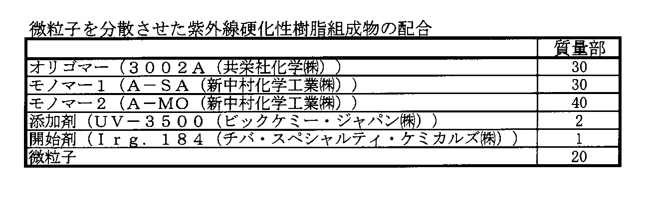
また、表1の配合において、微粒子を含まない紫外線硬化性樹脂組成物の屈折率は1.5であった。
[評価方法]
(1)コントラスト
1で作成した情報表示用パネルの基板に設けた電極への印加電圧を-200[V]~+200[V]まで10[V]ごとに変化させ、それぞれの表示状態において反射率を測定し、同絶対値の電圧印加時の白表示時反射率と黒表示時反射率の比をその電圧におけるコントラスト比とし、±200[V]印加時のコントラスト比を初期C200(=表2中、コントラストと記載)として表示媒体用粒子の鮮明表示性の指標とした。
(1)コントラスト
1で作成した情報表示用パネルの基板に設けた電極への印加電圧を-200[V]~+200[V]まで10[V]ごとに変化させ、それぞれの表示状態において反射率を測定し、同絶対値の電圧印加時の白表示時反射率と黒表示時反射率の比をその電圧におけるコントラスト比とし、±200[V]印加時のコントラスト比を初期C200(=表2中、コントラストと記載)として表示媒体用粒子の鮮明表示性の指標とした。
このコントラストが、4より小さい場合は×、4~5の場合は△、6より大きい場合は○として評価した。
(2)明るさ
情報表示用パネルの明るさの測定は、分光光度輝度計U-4000を用い、20度円環で拡散反射率から視感度反射率を求める方法でおこなった。このパネル反射率が大きくなると透過率が下がり明るさが低下する、すなわち、パネルの黒表示時と白表示時の差が小さくなる。
情報表示用パネルの明るさの測定は、分光光度輝度計U-4000を用い、20度円環で拡散反射率から視感度反射率を求める方法でおこなった。このパネル反射率が大きくなると透過率が下がり明るさが低下する、すなわち、パネルの黒表示時と白表示時の差が小さくなる。
従って、明るさの評価としては、パネル反射率が20%より小さい場合を○、20%より大きい場合を△として評価した。
以下、実施例1~9及び比較例において作製した情報表示用パネルのコントラスト及び明るさに関する評価を表2に記す。
本発明の情報表示用パネルの製造方法によれば、入力電力部おける電極の腐食等が防止された情報表示用パネルを高い生産性で製造することができる。従って本発明によりノートパソコン、電子手帳、PDA(Personal Digital Assistants)と呼ばれる携帯型情報機器、携帯電話、ハンディーターミナル等のモバイル機器の表示部、電子書籍、電子新聞、電子マニュアル(取扱説明書)等の電子ペーパー、電子看板(デジタルサイネージ)、ポスター、黒板(ホワイトボード)等の掲示板、電子卓上計算機、家電製品、自動車用品等の表示部、ポイントカード、ICカード等のカード表示部、電子広告、情報ボード、電子POP(Point Of Presence、Point Of Purchase advertising)、電子値札、電子棚札、電子楽譜、RF-ID機器の表示部、POS端末、カーナビゲーション装置、時計など様々な電子機器の表示部、及び書き換え装置に装着して表示書き換えを行うリライタブルペーパーを高品質に且つ低コストで製造することができる。
11、12、21、22、31、32、51、52:基板
13、23:表示媒体
13B、23B:黒色表示媒体
13Ba、23Ba:表示用黒色粒子
13W、23W、33W:白色表示媒体
13Wa、23Wa、33Wa:表示用白色粒子
37B:黒色板
14、24、34、54:隔壁
15、16、25、26、35、36:電極
40:金型
41:隔壁形成パターン領域
42:金型凹部
44:金型凸部
46:表示面側基板
48:紫外線硬化性樹脂組成物
48b:硬化した紫外線硬化性樹脂組成物
50:微粒子
53:情報表示領域
55:セル空間
60:情報表示用パネル
100:金型凸部‐基板間空間
100b:残膜
13、23:表示媒体
13B、23B:黒色表示媒体
13Ba、23Ba:表示用黒色粒子
13W、23W、33W:白色表示媒体
13Wa、23Wa、33Wa:表示用白色粒子
37B:黒色板
14、24、34、54:隔壁
15、16、25、26、35、36:電極
40:金型
41:隔壁形成パターン領域
42:金型凹部
44:金型凸部
46:表示面側基板
48:紫外線硬化性樹脂組成物
48b:硬化した紫外線硬化性樹脂組成物
50:微粒子
53:情報表示領域
55:セル空間
60:情報表示用パネル
100:金型凸部‐基板間空間
100b:残膜
Claims (8)
- 少なくとも一方が透明な対向する2枚の基板の一方の基板の表面に、インプリント法により隔壁を形成して、その基板間に当該隔壁により画成された多数のセルからなる空間を設け、それぞれの空間に帯電性を有する多数の粒子から構成される表示媒体を封入することにより、電界の付与によって前記表示媒体を移動させて情報を表示する情報表示用パネルを製造する方法であって、
前記隔壁を形成する隔壁材料が、微粒子を含む樹脂組成物からなり、且つ当該微粒子の屈折率が、前記樹脂組成物の基材樹脂の屈折率と異なることを特徴とする情報表示用パネルの製造方法。 - 前記微粒子の屈折率(np)が、下記式(I):

- 前記微粒子が、無機微粒子であることを特徴とする請求項1又は2に記載の方法。
- 前記微粒子の屈折率が、1.20~2.30であることを特徴とする請求項1~3の何れか1項に記載の方法。
- 前記微粒子の平均粒径が、50~150であることを特徴とする請求項1~4の何れか1項に記載の方法。
- 前記無機微粒子が、シリカ(SiO2)、酸化アンチモン(III)(Sb2O3)、酸化錫(SnO2)、及び酸化アルミニウム(Al2O3)からなる群から選択される少なくとも1種であることを特徴とする請求項3に記載の方法。
- 前記樹脂組成物が、紫外線硬化性樹脂組成物であることを特徴とする請求項1~6に記載の方法。
- 請求項1~7の何れか1項に記載の情報表示用パネルの製造方法によって製造されたことを特徴とする情報表示用パネル。
Applications Claiming Priority (2)
| Application Number | Priority Date | Filing Date | Title |
|---|---|---|---|
| JP2010-239300 | 2010-10-26 | ||
| JP2010239300A JP2012093469A (ja) | 2010-10-26 | 2010-10-26 | 情報表示用パネルの製造方法及び情報表示用パネル |
Publications (1)
| Publication Number | Publication Date |
|---|---|
| WO2012057056A1 true WO2012057056A1 (ja) | 2012-05-03 |
Family
ID=45993765
Family Applications (1)
| Application Number | Title | Priority Date | Filing Date |
|---|---|---|---|
| PCT/JP2011/074392 Ceased WO2012057056A1 (ja) | 2010-10-26 | 2011-10-24 | 情報表示用パネルの製造方法及び情報表示用パネル |
Country Status (2)
| Country | Link |
|---|---|
| JP (1) | JP2012093469A (ja) |
| WO (1) | WO2012057056A1 (ja) |
Families Citing this family (1)
| Publication number | Priority date | Publication date | Assignee | Title |
|---|---|---|---|---|
| KR102774486B1 (ko) * | 2020-09-08 | 2025-02-28 | 이 잉크 코포레이션 | 전기영동 디스플레이를 위한 반사성 마이크로셀 및 그 제조 방법 |
Citations (6)
| Publication number | Priority date | Publication date | Assignee | Title |
|---|---|---|---|---|
| JP2004302456A (ja) * | 2003-03-18 | 2004-10-28 | Canon Inc | 表示装置 |
| JP2005321769A (ja) * | 2004-04-07 | 2005-11-17 | Bridgestone Corp | 情報表示用パネル |
| JP2007034037A (ja) * | 2005-07-28 | 2007-02-08 | Canon Inc | 粒子移動型表示装置 |
| JP2008107749A (ja) * | 2006-09-28 | 2008-05-08 | Bridgestone Corp | 情報表示用パネル |
| JP2009294275A (ja) * | 2008-06-03 | 2009-12-17 | Brother Ind Ltd | 帯電粒子移動型表示パネル、帯電粒子移動型表示パネルの製造方法及び帯電粒子移動型表示装置 |
| JP2010008475A (ja) * | 2008-06-24 | 2010-01-14 | Toshiba Mobile Display Co Ltd | 液晶表示装置 |
-
2010
- 2010-10-26 JP JP2010239300A patent/JP2012093469A/ja active Pending
-
2011
- 2011-10-24 WO PCT/JP2011/074392 patent/WO2012057056A1/ja not_active Ceased
Patent Citations (6)
| Publication number | Priority date | Publication date | Assignee | Title |
|---|---|---|---|---|
| JP2004302456A (ja) * | 2003-03-18 | 2004-10-28 | Canon Inc | 表示装置 |
| JP2005321769A (ja) * | 2004-04-07 | 2005-11-17 | Bridgestone Corp | 情報表示用パネル |
| JP2007034037A (ja) * | 2005-07-28 | 2007-02-08 | Canon Inc | 粒子移動型表示装置 |
| JP2008107749A (ja) * | 2006-09-28 | 2008-05-08 | Bridgestone Corp | 情報表示用パネル |
| JP2009294275A (ja) * | 2008-06-03 | 2009-12-17 | Brother Ind Ltd | 帯電粒子移動型表示パネル、帯電粒子移動型表示パネルの製造方法及び帯電粒子移動型表示装置 |
| JP2010008475A (ja) * | 2008-06-24 | 2010-01-14 | Toshiba Mobile Display Co Ltd | 液晶表示装置 |
Also Published As
| Publication number | Publication date |
|---|---|
| JP2012093469A (ja) | 2012-05-17 |
Similar Documents
| Publication | Publication Date | Title |
|---|---|---|
| JP4657923B2 (ja) | 画像表示用パネルの製造方法 | |
| US7557982B2 (en) | Information display panel | |
| JP2012078547A (ja) | 情報表示用パネルの製造方法及び情報表示用パネル | |
| JP2012093469A (ja) | 情報表示用パネルの製造方法及び情報表示用パネル | |
| JP2012018254A (ja) | 情報表示用パネルの製造方法 | |
| JP2012002963A (ja) | 情報表示用パネルの製造方法 | |
| JP2008268772A (ja) | 情報表示用パネルの製造方法 | |
| CN101910933B (zh) | 信息显示面板及其制造方法 | |
| JP2006154655A (ja) | 情報表示用パネルの製造方法および情報表示装置 | |
| JPWO2011077668A1 (ja) | 情報表示用パネル及びその製造方法 | |
| JP2009271192A (ja) | 情報表示用パネル | |
| JP2013156313A (ja) | 情報表示用パネルの製造方法 | |
| JP4974515B2 (ja) | 情報表示用パネルの製造方法および情報表示装置 | |
| JP4863707B2 (ja) | 情報表示用パネルの製造方法および情報表示用パネル | |
| JPWO2010010954A1 (ja) | ドットマトリックス型情報表示用パネル | |
| JP4825502B2 (ja) | 情報表示用パネルの製造方法および情報表示装置 | |
| JP4776210B2 (ja) | 情報表示用パネルの製造方法及び情報表示用パネル | |
| JP4966559B2 (ja) | 情報表示用パネルの製造方法および情報表示用パネル | |
| JP2011227413A (ja) | 情報表示用パネルの製造方法及び情報表示パネル | |
| JP4925708B2 (ja) | 情報表示用パネルの製造方法 | |
| JP2012189963A (ja) | 情報表示用パネル | |
| JP2009080149A (ja) | 情報表示用パネル | |
| JP2006293154A (ja) | 情報表示用パネルの製造方法および情報表示用パネル | |
| JP2008076840A (ja) | 情報表示用パネルの製造方法 | |
| JP2007163660A (ja) | 情報表示用パネルの製造方法および情報表示用パネル |
Legal Events
| Date | Code | Title | Description |
|---|---|---|---|
| 121 | Ep: the epo has been informed by wipo that ep was designated in this application |
Ref document number: 11836190 Country of ref document: EP Kind code of ref document: A1 |
|
| NENP | Non-entry into the national phase |
Ref country code: DE |
|
| 122 | Ep: pct application non-entry in european phase |
Ref document number: 11836190 Country of ref document: EP Kind code of ref document: A1 |