WO2012057027A1 - タッチパネル、表示装置およびタッチパネルの製造方法 - Google Patents
タッチパネル、表示装置およびタッチパネルの製造方法 Download PDFInfo
- Publication number
- WO2012057027A1 WO2012057027A1 PCT/JP2011/074305 JP2011074305W WO2012057027A1 WO 2012057027 A1 WO2012057027 A1 WO 2012057027A1 JP 2011074305 W JP2011074305 W JP 2011074305W WO 2012057027 A1 WO2012057027 A1 WO 2012057027A1
- Authority
- WO
- WIPO (PCT)
- Prior art keywords
- electrode
- transparent conductive
- film
- conductive film
- touch panel
- Prior art date
- Legal status (The legal status is an assumption and is not a legal conclusion. Google has not performed a legal analysis and makes no representation as to the accuracy of the status listed.)
- Ceased
Links
Images












Classifications
-
- G—PHYSICS
- G02—OPTICS
- G02F—OPTICAL DEVICES OR ARRANGEMENTS FOR THE CONTROL OF LIGHT BY MODIFICATION OF THE OPTICAL PROPERTIES OF THE MEDIA OF THE ELEMENTS INVOLVED THEREIN; NON-LINEAR OPTICS; FREQUENCY-CHANGING OF LIGHT; OPTICAL LOGIC ELEMENTS; OPTICAL ANALOGUE/DIGITAL CONVERTERS
- G02F1/00—Devices or arrangements for the control of the intensity, colour, phase, polarisation or direction of light arriving from an independent light source, e.g. switching, gating or modulating; Non-linear optics
- G02F1/01—Devices or arrangements for the control of the intensity, colour, phase, polarisation or direction of light arriving from an independent light source, e.g. switching, gating or modulating; Non-linear optics for the control of the intensity, phase, polarisation or colour
- G02F1/13—Devices or arrangements for the control of the intensity, colour, phase, polarisation or direction of light arriving from an independent light source, e.g. switching, gating or modulating; Non-linear optics for the control of the intensity, phase, polarisation or colour based on liquid crystals, e.g. single liquid crystal display cells
- G02F1/133—Constructional arrangements; Operation of liquid crystal cells; Circuit arrangements
- G02F1/1333—Constructional arrangements; Manufacturing methods
- G02F1/13338—Input devices, e.g. touch panels
-
- G—PHYSICS
- G06—COMPUTING OR CALCULATING; COUNTING
- G06F—ELECTRIC DIGITAL DATA PROCESSING
- G06F3/00—Input arrangements for transferring data to be processed into a form capable of being handled by the computer; Output arrangements for transferring data from processing unit to output unit, e.g. interface arrangements
- G06F3/01—Input arrangements or combined input and output arrangements for interaction between user and computer
- G06F3/03—Arrangements for converting the position or the displacement of a member into a coded form
- G06F3/041—Digitisers, e.g. for touch screens or touch pads, characterised by the transducing means
- G06F3/0412—Digitisers structurally integrated in a display
-
- G—PHYSICS
- G06—COMPUTING OR CALCULATING; COUNTING
- G06F—ELECTRIC DIGITAL DATA PROCESSING
- G06F3/00—Input arrangements for transferring data to be processed into a form capable of being handled by the computer; Output arrangements for transferring data from processing unit to output unit, e.g. interface arrangements
- G06F3/01—Input arrangements or combined input and output arrangements for interaction between user and computer
- G06F3/03—Arrangements for converting the position or the displacement of a member into a coded form
- G06F3/041—Digitisers, e.g. for touch screens or touch pads, characterised by the transducing means
- G06F3/0416—Control or interface arrangements specially adapted for digitisers
- G06F3/04164—Connections between sensors and controllers, e.g. routing lines between electrodes and connection pads
-
- G—PHYSICS
- G06—COMPUTING OR CALCULATING; COUNTING
- G06F—ELECTRIC DIGITAL DATA PROCESSING
- G06F3/00—Input arrangements for transferring data to be processed into a form capable of being handled by the computer; Output arrangements for transferring data from processing unit to output unit, e.g. interface arrangements
- G06F3/01—Input arrangements or combined input and output arrangements for interaction between user and computer
- G06F3/03—Arrangements for converting the position or the displacement of a member into a coded form
- G06F3/041—Digitisers, e.g. for touch screens or touch pads, characterised by the transducing means
- G06F3/044—Digitisers, e.g. for touch screens or touch pads, characterised by the transducing means by capacitive means
-
- G—PHYSICS
- G06—COMPUTING OR CALCULATING; COUNTING
- G06F—ELECTRIC DIGITAL DATA PROCESSING
- G06F3/00—Input arrangements for transferring data to be processed into a form capable of being handled by the computer; Output arrangements for transferring data from processing unit to output unit, e.g. interface arrangements
- G06F3/01—Input arrangements or combined input and output arrangements for interaction between user and computer
- G06F3/03—Arrangements for converting the position or the displacement of a member into a coded form
- G06F3/041—Digitisers, e.g. for touch screens or touch pads, characterised by the transducing means
- G06F3/044—Digitisers, e.g. for touch screens or touch pads, characterised by the transducing means by capacitive means
- G06F3/0443—Digitisers, e.g. for touch screens or touch pads, characterised by the transducing means by capacitive means using a single layer of sensing electrodes
-
- G—PHYSICS
- G06—COMPUTING OR CALCULATING; COUNTING
- G06F—ELECTRIC DIGITAL DATA PROCESSING
- G06F3/00—Input arrangements for transferring data to be processed into a form capable of being handled by the computer; Output arrangements for transferring data from processing unit to output unit, e.g. interface arrangements
- G06F3/01—Input arrangements or combined input and output arrangements for interaction between user and computer
- G06F3/03—Arrangements for converting the position or the displacement of a member into a coded form
- G06F3/041—Digitisers, e.g. for touch screens or touch pads, characterised by the transducing means
- G06F3/044—Digitisers, e.g. for touch screens or touch pads, characterised by the transducing means by capacitive means
- G06F3/0446—Digitisers, e.g. for touch screens or touch pads, characterised by the transducing means by capacitive means using a grid-like structure of electrodes in at least two directions, e.g. using row and column electrodes
-
- G—PHYSICS
- G02—OPTICS
- G02F—OPTICAL DEVICES OR ARRANGEMENTS FOR THE CONTROL OF LIGHT BY MODIFICATION OF THE OPTICAL PROPERTIES OF THE MEDIA OF THE ELEMENTS INVOLVED THEREIN; NON-LINEAR OPTICS; FREQUENCY-CHANGING OF LIGHT; OPTICAL LOGIC ELEMENTS; OPTICAL ANALOGUE/DIGITAL CONVERTERS
- G02F1/00—Devices or arrangements for the control of the intensity, colour, phase, polarisation or direction of light arriving from an independent light source, e.g. switching, gating or modulating; Non-linear optics
- G02F1/01—Devices or arrangements for the control of the intensity, colour, phase, polarisation or direction of light arriving from an independent light source, e.g. switching, gating or modulating; Non-linear optics for the control of the intensity, phase, polarisation or colour
- G02F1/13—Devices or arrangements for the control of the intensity, colour, phase, polarisation or direction of light arriving from an independent light source, e.g. switching, gating or modulating; Non-linear optics for the control of the intensity, phase, polarisation or colour based on liquid crystals, e.g. single liquid crystal display cells
- G02F1/133—Constructional arrangements; Operation of liquid crystal cells; Circuit arrangements
- G02F1/1333—Constructional arrangements; Manufacturing methods
- G02F1/1345—Conductors connecting electrodes to cell terminals
- G02F1/13456—Cell terminals located on one side of the display only
-
- G—PHYSICS
- G06—COMPUTING OR CALCULATING; COUNTING
- G06F—ELECTRIC DIGITAL DATA PROCESSING
- G06F2203/00—Indexing scheme relating to G06F3/00 - G06F3/048
- G06F2203/041—Indexing scheme relating to G06F3/041 - G06F3/045
- G06F2203/04103—Manufacturing, i.e. details related to manufacturing processes specially suited for touch sensitive devices
-
- G—PHYSICS
- G06—COMPUTING OR CALCULATING; COUNTING
- G06F—ELECTRIC DIGITAL DATA PROCESSING
- G06F2203/00—Indexing scheme relating to G06F3/00 - G06F3/048
- G06F2203/041—Indexing scheme relating to G06F3/041 - G06F3/045
- G06F2203/04111—Cross over in capacitive digitiser, i.e. details of structures for connecting electrodes of the sensing pattern where the connections cross each other, e.g. bridge structures comprising an insulating layer, or vias through substrate
Definitions
- the present invention relates to a touch panel, a display device, and a touch panel manufacturing method, and more particularly, to a touch panel, a display device, and a touch panel manufacturing method for detecting a capacitance formed between a touch object and a contact object.
- touch panels have been widely used as input means.
- the touch panel is arranged on a screen of a display device such as a liquid crystal display device or a plasma display, and a user can input and output information by performing various operations on the operation surface with a finger or a pen. it can.
- the touch panel includes a transparent operation unit facing the screen of the display device, and a peripheral unit provided around the operation unit and provided with a plurality of terminals.
- touch panel methods There are a plurality of types of touch panel methods, and representative methods include a capacitance method, an electromagnetic induction method, and a resistive film method.
- a capacitive touch panel is provided on a transparent substrate, a plurality of electrodes provided on a portion of the transparent substrate where the operation unit is located, a wire having one end connected to the electrode, and the other end of the wire. And a protective film for protecting the electrodes and the like.
- the electrode forms a capacitance with a contact object such as a finger or a pen that comes into contact with the surface of the operation unit. Then, by passing a current through the electrode, it is possible to detect a change in the capacitance of the electrode and to know the presence or absence of a contact object. Furthermore, a contact position can be detected by arranging a plurality of striped electrodes in a mesh pattern and passing a current through each electrode in a time-sharing manner.
- the terminal portion is generally provided on the outer peripheral side of the transparent substrate, and an external terminal is fitted into this terminal. Signals are input / output from the external terminals.
- touch panels are not limited to capacitive touch panels, and electrodes for detecting contact objects, wiring connected to the electrodes, terminal portions formed at the ends of the wiring, wiring and electrodes And a protective film for protecting the film.
- a liquid crystal display device also includes a gate terminal portion connected to a bus line and connected to an external terminal.
- a semiconductor layer of a TFT element or the like is formed around the gate terminal portion, and the terminal portion provided on the touch panel and the gate terminal portion of the liquid crystal display device have completely different structures. Yes.
- a touch panel includes an interlayer insulating film formed on a wiring, a protective film is formed on the interlayer insulating film, and a terminal portion is provided on the bottom surface of a contact hole that penetrates the interlayer insulating film and the protective film.
- the transparent conductive film is formed.
- the external terminal may be removed from the touch panel when reworking the flexible substrate of the external terminal connected to the terminal portion of the touch panel.
- the protective film may be peeled off together with the external terminals. Further, when the protective film is formed of an inorganic material, when the external terminal is removed, the protective film and the external terminal may come into contact with each other to cause a crack in the protective film. When a crack occurs in the protective film, moisture in the atmosphere may enter the touch panel and the wiring may be corroded. In addition, when connecting an external terminal, a protective film and an external terminal may contact similarly and a crack may arise in a protective film.
- the terminal portion is formed only from the ITO film that is drawn from the end of the wiring to the outer peripheral edge of the transparent substrate and exposed from the protective film and the interlayer insulating film.
- the terminal portion becomes a portion exposed from the protective film and the interlayer insulating film in the ITO film extending on the transparent substrate, and the electrical resistance of the terminal portion is increased. Furthermore, since the ITO film and the transparent substrate located under the ITO film transmit light, it is difficult to perform trace inspection of the terminal portion.
- the present invention has been made in view of the problems as described above, and its purpose is to suppress the peeling of the protective film and the occurrence of cracks when attaching / detaching the external terminal, and to perform inspection such as trace inspection. It is providing the manufacturing method of a touch panel provided with the terminal part which can perform, a display apparatus, and a touch panel.
- the touch panel according to the present invention is a touch panel that has a touch surface and detects a contact position of a contact object that contacts the touch surface.
- the touch panel includes: a transparent substrate having a first main surface; a plurality of wirings formed on the first main surface of the transparent substrate; an interlayer insulating film formed on the first main surface and covering the wiring; Connected touch electrodes.
- the touch panel includes a protective film formed on the interlayer insulating film so as to cover the touch electrode, and a plurality of terminal portions connected to the wiring and arranged along the outer peripheral edge portion of the transparent substrate.
- the protective film is located on the side opposite to the outer peripheral edge of the transparent substrate with respect to the terminal portion, and the wiring includes an extending portion extending toward the outer peripheral edge of the transparent substrate rather than the protective film.
- a contact hole reaching the extension is formed in a portion of the interlayer insulating film that covers the extension, and the terminal transparent conductive material for terminals formed on the upper surface of the extension located at the bottom of the contact hole Including membrane.
- the terminal transparent conductive film is formed so as to cover the upper surface of the extending portion located at the bottom of the contact hole and the inner peripheral surface of the contact hole and reach the upper surface of the interlayer insulating film.
- the extending portion is located inside the terminal transparent conductive film.
- the extension includes a metal wiring and a coated transparent conductive film that covers the metal wiring.
- the terminal transparent conductive film is formed on the coated transparent conductive film.
- the protective film includes an organic insulating film. The upper surface of the organic insulating film is a touch surface.
- the transparent substrate includes a second main surface located opposite to the first main surface on which the wiring is formed, and the touch panel further includes a color filter formed on the second main surface.
- a display device includes the touch panel.
- a method for manufacturing a touch panel includes a step of preparing a transparent substrate including a panel formation region, a step of forming a plurality of wirings whose end portions are arranged along an outer peripheral edge of the panel formation region, and a wiring.
- the method includes a step of forming an interlayer insulating film formed to cover and a step of forming a touch electrode connected to the wiring.
- a method of manufacturing a touch panel includes a step of forming a contact hole reaching an end of a wiring in an interlayer insulating film, a step of forming a transparent conductive film for a terminal connected to the upper surface of the wiring located at the bottom of the contact hole, and a terminal Forming a first insulating film on the interlayer insulating film so as to cover the touch electrode after forming the transparent conductive film, and a first insulating film so that the edge of the first insulating film is separated from the outer peripheral edge of the panel formation region. 1 patterning an insulating film to expose the transparent conductive film for terminals.
- the end of the wiring is exposed from the first insulating film by patterning the first insulating film.
- the terminal transparent conductive film is formed so as to reach the upper surface of the interlayer insulating film and cover the end portion of the wiring exposed from the first insulating film.
- the step of forming the touch electrode includes a step of forming a first transparent conductive film on the panel formation region, and a plurality of patterns formed by patterning the first transparent conductive film and spaced in the first direction. Forming a first electrode piece and a second electrode extending between the first electrode pieces and extending in a direction orthogonal to the first direction.
- the step of forming the touch electrode includes a step of forming a first electrode piece, a second electrode, and an electrode contact hole reaching the first electrode piece in an interlayer insulating film formed so as to cover the wiring.
- the said terminal transparent conductive film is formed with a connection part by patterning a 2nd transparent conductive film.
- the step of forming the touch electrode includes a step of forming a first transparent conductive film on the panel formation region, and patterning the first transparent conductive film to form a plurality of pieces arranged at intervals. Forming.
- a first electrode contact hole reaching one end of the piece and a second electrode contact hole reaching the other end of the piece are formed in an interlayer insulating film covering the piece and the wiring.
- the step of forming the touch electrode includes patterning the second transparent conductive film, the first electrode piece connected to one end of the piece through the first electrode contact hole, and the first electrode piece.
- a first electrode including a second electrode piece provided at a distance in one direction and passing through a second electrode contact hole and connected to the other end of the piece; a first electrode piece; and a second electrode piece; Forming a second electrode formed so as to pass therethrough.
- the terminal transparent conductive film is formed by patterning the second transparent conductive film.
- the step of forming the wiring includes a step of forming a metal film on the panel formation region, and a step of patterning the metal film to form a metal wiring. It includes a step of forming a transparent conductive film in the formation region and a step of patterning the transparent conductive film. By patterning the transparent conductive film, a coated transparent conductive film covering the metal wiring is formed.
- the touch panel, the display device, and the touch panel manufacturing method according to the present invention it is possible to suppress the peeling of the protective film and the occurrence of cracks when attaching / detaching the external terminals, and it is possible to perform inspections such as trace inspection.
- FIG. 1 is a cross-sectional view schematically showing a display device 100 according to a first embodiment. It is a top view which shows typically the opposing board
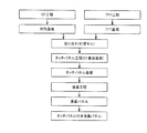
- FIG. 10 is a manufacturing flow diagram illustrating a first modification of the manufacturing flow of the liquid crystal display device 1.
- FIG. 10 is a manufacturing flow diagram illustrating a second modification of the manufacturing flow of the liquid crystal display device 1. It is a top view which shows a part of counter substrate 2 with a touchscreen which concerns on this Embodiment 2.
- FIG. It is a top view which shows a terminal part and the structure of the circumference
- FIG. 29 is a cross-sectional view showing a manufacturing step after the manufacturing step shown in FIG. 28.
- FIG. 30 is a cross-sectional view showing a manufacturing step after the manufacturing step shown in FIG. 29;
- FIG. 31 is a cross-sectional view showing a manufacturing step after the manufacturing step shown in FIG. 30.
- FIG. 32 is a cross-sectional view showing a manufacturing step after the manufacturing step shown in FIG. 31.
- a touch panel, a liquid crystal display device and a manufacturing method thereof according to the present invention will be described.
- a touch panel-equipped counter substrate integrated with a color filter or the like is adopted as the touch panel, but the touch panel is limited to an example integrated with a color filter. I can't.
- a counter substrate on which a color filter or the like is formed may be a separate touch panel.
- an example in which the present invention is applied to a liquid crystal display device with a touch function will be described.
- the present invention is not limited to a liquid crystal display device, and is not limited to a liquid crystal display device, but a plasma display panel (PDP) or an organic EL display (organic electroluminescence). display).
- PDP plasma display panel
- organic EL display organic electroluminescence
- FIG. 1 is a cross-sectional view schematically showing the display device 100 according to the first embodiment.
- the display device 100 includes a liquid crystal display device 1, a counter substrate 2 with a touch panel, and a case (not shown) that houses the liquid crystal display device 1 and the counter substrate 2 with a touch panel.
- the liquid crystal display device 1 is disposed so as to face the shared electrode 4, the color filter 3 formed on the lower surface of the transparent substrate of the counter substrate 2 with a touch panel, the shared electrode 4 formed on the lower surface side of the color filter 3.
- a TFT substrate (active matrix substrate) 5 and a backlight 7 for irradiating light toward the TFT substrate 5 are provided.
- a polarizing plate is provided between the TFT substrate 5 and the backlight 7, and a polarizing plate is also provided on the color filter 3.
- the TFT substrate 5 includes a plurality of TFT transistors (thin film transistors) and pixel electrodes connected to the drain electrodes of the TFT transistors. A potential is selectively applied to the pixel electrode by switching ON / OFF of the TFT transistor.
- the color filter 3 includes, for example, a red filter unit, a blue filter unit, a green filter unit, and a yellow filter unit, and selectively blocks light passing through each filter unit, thereby displaying an image on a liquid crystal display. It can be displayed in the display area of the device 1.
- the counter substrate 2 with a touch panel is formed on the upper surface of the liquid crystal display device 1 as described above.
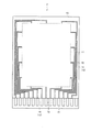
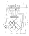
- FIG. 2 is a plan view schematically showing the counter substrate 2 with a touch panel.
- the counter substrate 2 with a touch panel includes a transparent substrate 10 formed in a square shape, and includes a touch surface 11 on which a user performs a touch operation, and a peripheral region 14 positioned around the touch surface 11.
- the counter substrate 2 with a touch panel is formed in a square shape, the touch surface 11 is located at the center of the counter substrate 2 with a touch panel, and the peripheral region 14 is along the four sides (outer peripheral edge) of the counter substrate 2 with a touch panel. It is formed in a ring shape.
- the touch surface 11 is located on the display area of the liquid crystal display device 1, and the peripheral area 14 is disposed on the non-display area of the liquid crystal display device 1.
- the touch surface 11 is exposed to the outside from a window portion formed in the housing, and the peripheral area 14 is covered with a frame portion of the housing.
- the peripheral region 14 includes a wiring region 13 in which a plurality of wirings 20 connected to electrodes are arranged, and a terminal region 12 in which terminal portions 21 provided at the ends of the wirings 20 are arranged.
- the terminal region 12 extends along one side of the transparent substrate 10
- the wiring region 13 extends along the remaining three sides of the transparent substrate 10.
- the touch surface 11 and the wiring region 13 are covered with a protective film 70 formed on the transparent substrate 10, and the terminal region 12 is formed so as to be exposed from the protective film 70.
- the terminal portions 21 are arranged along one side of the transparent substrate 10.
- FIG. 3 is a plan view schematically showing a part of the counter substrate 2 with a touch panel.
- FIG. 4 is a plan view showing the terminal portion 21 and the surrounding structure.
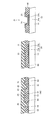
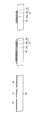
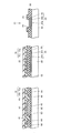
- FIG. 5 is a cross-sectional view of the counter substrate 2 with a touch panel.
- the cross-section located at the left end is a cross-sectional view taken along the line VA-VA shown in FIG. 3
- the cross-sectional view shown at the center is a cross-sectional view taken along the line VB-VB shown in FIGS. is there.
- the cross-sectional view shown at the right end is a cross-sectional view taken along the line VC-VC shown in FIGS. 3 and 4.
- a touch electrode 40 is formed on a portion of the main surface of the transparent substrate 10 where the touch surface 11 is located.
- the touch electrode 40 includes a plurality of first electrode rows 41 extending in the first direction and a plurality of second electrode rows 42 extending in a second direction orthogonal to the first direction.
- the first electrode rows 41 are arranged at intervals in the second direction, and the second electrode rows 42 are arranged at intervals in the first direction.
- the first electrode row 41 includes a plurality of electrode pieces 44 arranged at intervals in the first direction, and a connection portion 43 that connects the adjacent electrode pieces 44 to each other.
- the electrode piece 44 is formed in a square shape, and the connection portion 43 connects the apex portions of the electrode pieces 44 to each other.
- the second electrode row 42 also includes a plurality of electrode pieces 47 arranged at intervals in the second direction, and a connection portion 48 that connects the adjacent electrode pieces 47 to each other.
- the electrode piece 47 is also formed in a square shape, and the connection portion 48 is formed so as to connect the apex portions of the electrode pieces 47.
- the first electrode row 41 and the second electrode row 42 are formed of a transparent conductive film such as an ITO (Indium Tin Oxide) film or an IZO (Indium Zinc Oxide) film.
- a transparent conductive film such as an ITO (Indium Tin Oxide) film or an IZO (Indium Zinc Oxide) film.
- the counter substrate 2 with a touch panel is formed on the interlayer insulating film 60 formed on the main surface of the transparent substrate 10 so as to cover the wiring 20 and on the interlayer insulating film 60 so as to cover the touch electrode 40.
- a plurality of contact holes 45 and contact holes 46 are formed in the interlayer insulating film 60, including the formed protective film 70.
- the wiring 20 is a laminated metal film including a metal film 20a and a metal film 20b formed on the metal film 20a.
- the metal film 20a is made of, for example, aluminum (Al)
- the metal film 20b is made of, for example, molybdenum niobium (MoNb).
- the interlayer insulating film 60 is formed of, for example, an inorganic insulating film such as a SiN film or an acrylic-based resinous organic insulating film.
- the protective film 70 is formed of an acrylic-based organic insulating film.
- the protective film 70 is formed of a transparent resin layer such as an organic insulating film, and the upper surface of the protective film 70 is used as a touch surface. It is possible to suppress the occurrence.
- the protective film 70 may be a laminated film of an inorganic insulating film such as a SiN film formed on the interlayer insulating film 60 and an acrylic-based organic insulating film formed on the inorganic insulating film.
- connection portion 43 is formed on the interlayer insulating film 60 so as to connect the upper surface of the electrode piece 44 located at the bottom of the contact hole 46 and the upper surface of another electrode piece 44 located at the bottom of the contact hole 45. Yes.
- the second electrode row 42 is formed on the main surface of the transparent substrate 10 so as to pass below the connection portion 43.
- the first electrode row 41 is connected to the wiring 20, and the second electrode row 42 is also connected to the wiring 20.
- connection portion 50 The apex portion of the electrode piece 47 located at one end of the second electrode row 42 and the pad portion 54 formed at the end portion of the wiring 20 are connected by the connection portion 50. Note that one end of the connection portion 50 is connected to the electrode piece 47 through a contact hole, and the other end of the connection portion 50 is connected to the pad portion 54 through the contact hole.
- the apex portion of the electrode piece 44 positioned at one end of the first electrode row 41 and the pad portion 55 formed at the end portion of the wiring 20 are connected by the connecting portion 52.
- One end of the connecting portion 52 passes through the contact hole and is connected to the apex portion of the electrode piece 44, and the other end of the connecting portion 52 passes through the contact hole and is connected to the pad portion 55.
- each wiring 20 is connected to a terminal part 21, and an external terminal (not shown) is connected to the terminal part 21, and this external terminal is connected to a control part.
- a capacitance is formed between the first electrode array 41 facing the contact object and the contact object.
- a capacitance is also formed between the second electrode row 42 facing the contact object and the contact object.
- the protective film 70 is disposed on the side opposite to the outer peripheral edge of the transparent substrate 10 with respect to the terminal portion 21, and the wiring 20 extends to the outer peripheral edge of the transparent substrate 10 with respect to the protective film 70.
- the extension part 23 is included. 4 and 5, the transparent conductive film 25 is formed of a transparent conductive film such as an ITO film or an IZO film.
- a contact hole 24 exposing a part of the upper surface of the extension 23 is formed in the interlayer insulating film 60, and the transparent conductive film 25 passes through the upper surface of the extension 23 and the inner peripheral surface of the contact hole 24.
- the interlayer insulating film 60 is formed to reach the upper surface.
- the transparent conductive film 25 extends along the inner peripheral surface of the contact hole 24 and the upper surface of the extension portion 23 to form a recess, and the terminal portion of the external terminal is inserted into the recess.
- the terminal portion 21 includes a portion of the transparent conductive film 25 that is located on the upper surface of the extending portion 23.
- the terminal part 21 and an external terminal are connected by inserting the terminal part of an external terminal into the said recessed part.
- the protective film 70 is not formed around the terminal portion 21 (contact hole 24), and the protective film 70 is provided at a distance from the contact hole 24. ing.
- the extension portion 23 Since the transparent conductive film 25 is formed on the metal film 20a, the extension portion 23 does not transmit light when the trace inspection is performed with the external terminal removed from the terminal portion 21. 25 damages and scars can be observed well.
- the transparent conductive film 25 is formed so as to reach the upper surface of the transparent substrate 10, the upper surface of the interlayer insulating film 60 positioned around the contact hole 24 when the terminal portion of the external terminal is connected to the terminal portion 21. It is possible to prevent the external terminals from coming into direct contact with each other, and the interlayer insulating film 60 can be protected.
- the transparent conductive film 25 and the extension part 23 are observed from a direction perpendicular to the transparent substrate 10, the transparent conductive film 25 is formed so as to cover the extension part 23. It is disposed inside the transparent conductive film 25.
- the transparent conductive film 25 can function as an etching stopper when the protective film 70 is patterned so that the terminal region 12 is exposed from the protective film 70. Even if the etching is performed on the interlayer insulating film, the interlayer insulating film can be left so as to cover the extending portion 23.
- the protective film 70 when the protective film 70 is patterned, it is possible to prevent the interlayer insulating film located on the extending portion 23 from being removed, and even the extending portion 23 can be prevented from being etched. Can be suppressed.
- the transparent conductive film 25 extends under the protective film 70, and even when mask misalignment occurs when the protective film 70 is patterned, the interlayer insulating film located under the transparent conductive film 25 is etched. Can be prevented.
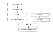
- FIG. 12 is a manufacturing flow diagram showing a manufacturing flow for manufacturing the liquid crystal display device 1.
- the counter substrate 2 with a touch panel and the TFT substrate 5 are manufactured in separate processes.
- the TFT process for forming the TFT substrate 5 includes a step of preparing a mother transparent substrate in which a plurality of panel formation regions are defined, a step of forming gate wiring on the main surface of the mother transparent substrate where the panel formation region is located, Forming a gate insulating film on the gate wiring. Further, the step of forming the TFT substrate 5 includes a step of forming a semiconductor layer on the gate insulating film, a step of forming a source electrode, a source wiring and a drain electrode on the semiconductor layer, and covering the source wiring and the like.
- the counter substrate 2 with a touch panel When manufacturing the counter substrate 2 with a touch panel, first, a mother transparent substrate in which a plurality of panel formation areas are defined is prepared, and electrodes and wirings of the touch panel are formed on each panel formation area (touch panel process). A touch panel substrate is formed through this process. Thereafter, a color filter and a shared electrode are formed on the main surface opposite to the main surface on which the electrodes and wirings of the patch panel are formed (CF process). Then, the counter substrate 2 with a touch panel is manufactured by cutting the mother transparent substrate.
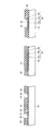
- the cross-sectional view located at the left end is a cross-sectional view taken along the line VA-VA shown in FIG.
- the cross-sectional view located at the center is a cross-sectional view taken along the line VB-VB in FIGS. 3 and 4, and the cross-sectional view located at the right end is a cross-sectional view taken along the line VC-VC in FIGS.
- FIG. 6 is a cross-sectional view showing a first manufacturing process of manufacturing the touch panel of the counter substrate 2 with a touch panel. As shown in FIG. 6, first, a mother transparent substrate 80 having a main surface is prepared. A plurality of panel formation regions are defined on the main surface of the mother transparent substrate 80.
- a metal film 20a and a metal film 20b are sequentially deposited on the main surface of the mother transparent substrate 80, and each metal film 20a and the metal film 20b are patterned. Thereby, the wiring 20 is formed.
- a transparent conductive film such as an ITO film or an IZO film is formed on the main surface of the mother transparent substrate 80.
- a plurality of electrode pieces 44 and a second electrode array 42 are formed on the main surface of the mother transparent substrate 80.
- an interlayer insulating film 60 such as a SiN film is deposited on the main surface of the mother transparent substrate 80.
- the interlayer insulating film 60 is formed so as to cover the electrode piece 44, the second electrode row 42, and the wiring 20.
- the interlayer insulating film 60 is patterned to reach the upper surfaces of the contact holes 45 and 46 reaching the end of the electrode piece 44 and the portion of the wiring 20 that will become the extension 23.
- a contact hole 24 is formed.
- a transparent conductive film such as an ITO film or an IZO film is deposited on the upper surface of the interlayer insulating film 60. And by patterning this transparent conductive film, the connection part 43 which connects adjacent electrode pieces 44 is formed, and the transparent conductive film 25 is formed.
- the terminal portion 21 can be formed in the process of forming the touch electrode 40, and the manufacturing process can be simplified. Can do.
- the transparent conductive film 25 covers a portion located at the bottom of the contact hole 24 among the upper surface of the portion that becomes the extension portion 23 and the inner peripheral surface of the contact hole 24, and reaches the upper surface of the interlayer insulating film 60. It is formed.
- the width of the transparent conductive film 25 is larger than the width of the extending portion 23, and the transparent conductive film 25 is formed so as to cover a portion that becomes the extending portion 23.
- the terminal part 21 including the part located on the upper surface of the part which becomes the extending part 23 in the transparent conductive film 25 is formed.
- an acrylic-based organic insulating film is deposited on the upper surface of the interlayer insulating film 60 so as to cover the connection portion 43 and the transparent conductive film 25. Then, the organic insulating film is patterned so that the outer peripheral edge of the organic insulating film is separated from the outer peripheral edge of the panel formation region. Thereby, the protective film 70 in which the terminal portion 21 exposes the organic insulating film to the outside is formed.
- an interlayer insulating film 60 can be obtained by employing an etchant having a high selection ratio between the protective film 70 and the interlayer insulating film 60. Can be prevented from being etched.
- the transparent conductive film 25 is formed so as to cover the extending portion 23, the transparent conductive film 25 functions as an etching stopper. For this reason, even when the organic insulating film is etched, even the interlayer insulating film 60 is etched, at least a portion of the terminal portion 21 covered with the transparent conductive film 25 can remain.
- the extension 23 can be prevented from being exposed to the outside, and the extension 23 can be prevented from being etched.
- the touch panel substrate shown in FIG. 12 can be manufactured through such steps. Thereafter, the main surface of the mother transparent substrate exposed to the outside is directed upward, and the color filter 3 and the shared electrode 4 are formed on the main surface.
- liquid crystal is dropped on the main surface of the TFT substrate 5 or the counter substrate 2 with a touch panel, and the TFT substrate 5 and the counter substrate 2 with a touch panel are bonded together (liquid crystal process). Thereby, a liquid crystal panel with a touch panel can be formed.
- the liquid crystal display device 1 can be manufactured by housing the liquid crystal panel, the backlight 7 and the optical module in the casing.
- FIG. 13 is a manufacturing flow diagram showing a first modification of the manufacturing flow of the liquid crystal display device 1.
- the counter substrate and the TFT substrate are manufactured in separate steps.
- a plurality of mother transparent substrates are prepared.
- a color filter and a shared electrode are formed on the main surface of the mother transparent substrate (CF process).
- the liquid crystal pre-process includes a PI printing process, a seal drawing process, a liquid crystal dropping injection process, and a bonding process.
- a polyimide (PI) film is printed on the main surface of the counter substrate and the TFT substrate 5.
- the polyimide film is subjected to a rubbing process or the like to form an alignment film.
- liquid crystal dropping / injecting step liquid crystal is dropped on the main surface of the counter electrode or the TFT substrate. Thereafter, in the bonding step, the counter substrate and the TFT substrate 5 are bonded together.
- the gap between the counter substrate and the TFT substrate is sealed. Thereafter, the transparent substrate of the counter substrate and the transparent substrate of the TFT substrate are wet-etched to thin each transparent substrate.
- the electrodes, wirings, terminal portions, interlayer insulating films, protective films, etc. of the touch panel are formed on the transparent substrate of the counter substrate.
- the chemical liquid is prevented from entering between the counter substrate and the TFT substrate in the touch panel process.
- the liquid crystal panel with a touch panel can be formed by passing through a liquid crystal back process.
- the liquid crystal display device 1 can be manufactured by housing the liquid crystal panel together with the backlight and the optical sheet in the housing.
- FIG. 14 is a manufacturing flow diagram showing a second modification of the manufacturing flow of the liquid crystal display device 1.
- the counter substrate and the TFT substrate are manufactured separately.
- the counter substrate and the TFT substrate are bonded together without sealing the liquid crystal (bonding process).
- the electrodes, wirings, interlayer insulating films, terminal portions, protective films, and the like of the touch panel are formed on the transparent substrate of the counter substrate. Thereby, the counter substrate 2 with a touch panel is formed.
- liquid crystal is sealed between the counter substrate 2 with a touch panel and the TFT substrate.
- the liquid crystal panel with a touch panel provided with the counter substrate 2 with a touch panel and the TFT substrate 5 is formed.
- the liquid crystal display device 1 can be manufactured by housing the liquid crystal panel together with the backlight and the optical sheet in the housing.
- FIG. 15 is a plan view showing a part of the counter substrate 2 with a touch panel according to the second embodiment.
- the counter substrate with a touch panel 2 according to the second embodiment also includes a transparent substrate 10 and a touch electrode 140 formed on a portion of the main surface of the transparent substrate 10 where the touch surface 11 is located. And a plurality of wirings 20 connected to the touch electrode 140 and a terminal portion 21 formed at an end of the wiring 20.
- the counter substrate 2 with a touch panel includes a protective film 70 formed to cover at least the touch electrode 140, and the terminal region 12 in which the plurality of terminal portions 21 are arranged is exposed from the protective film 70.
- the touch electrode 140 includes a plurality of first electrode rows 141 extending in the first direction and a plurality of second electrode rows 142 extending in the second direction.
- a plurality of first electrode rows 141 are formed at intervals in the second direction, and a plurality of second electrode rows 142 are formed at intervals in the first direction.
- the first electrode row 141 includes a plurality of electrode pieces 144 arranged at intervals in the first direction, and a connection portion 143 connecting the ends of the adjacent electrode pieces 144.
- the second electrode row 142 includes a plurality of electrode pieces 147 arranged at intervals in the second direction, and a connection portion 148 that connects adjacent electrode pieces 147 to each other.
- the wiring 20 includes an extending portion 23 that extends toward the outer peripheral edge of the transparent substrate 10 rather than the protective film 70.
- the terminal portion 21 is formed on the extending portion 23.
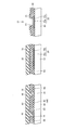
- FIG. 17 is a cross-sectional view of the counter substrate 2 with a touch panel. 17 is a cross-sectional view taken along line XVIA-XVIA shown in FIG. 17 is a cross-sectional view taken along the line XVIB-XVIB in FIGS. 15 and 16. 17 is a cross-sectional view taken along line XVIC-XVIC in FIGS. 15 and 16.
- connection part 143, the wiring 20 and the extension part 23 are formed on the main surface of the transparent substrate 10 so as to cover the connection part 143, the wiring 20 and the extension part 23.
- An interlayer insulating film 60 is formed.
- connection portion 143 may be formed of a transparent conductive film such as an ITO film or an IZO film, or may be a laminated conductive film of the metal film 20 a and the metal film 20 b as with the wiring 20.
- the interlayer insulating film 60 is formed so as to cover the connecting portion 143, the wiring 20, and the extending portion 23, and the interlayer insulating film 60 is formed of an inorganic insulating film such as a SiN film, for example.
- a contact hole 145 formed so as to reach the upper surface of one end portion of the connection portion 143 and a contact hole 146 formed so as to reach the upper surface of the other end portion of the connection portion 143 are formed. ing.
- One electrode piece 144 of the two adjacent electrode pieces 144 is connected to the connection portion 143 through the contact hole 146.
- the other electrode piece 144 is connected to the connection portion 143 through the contact hole 145.
- the first electrode row 141 is formed on the interlayer insulating film 60, and the second electrode row 142 is formed to extend between the electrode pieces 144.
- a protective film 70 is formed so as to cover the touch electrode 140.
- the protective film 70 includes an inorganic insulating film 70a formed on the interlayer insulating film 60 so as to cover the touch electrode 140, and an upper surface of the inorganic insulating film 70a. And an organic insulating film 70b formed on the substrate.
- the inorganic insulating film 70a is formed from, for example, a SiN film, and the organic insulating film 70b is formed from an acrylic-based resin.
- the contact object contacts the touch surface 11 or supports the counter substrate 2 with a touch panel with various support members during the manufacturing process of the counter substrate 2 with a touch panel. At this time, it is possible to suppress the generation of cracks or the like in the protective film 70. Furthermore, the insulating film 70 is improved in insulation performance by using the inorganic insulating film 70 a as the portion of the protective film 70 located on the touch electrode 140.
- the transparent conductive film 25 is formed so as to cover the extending portion 23.
- FIGS. 18 to 23 A method for manufacturing the counter substrate with a touch panel 2 configured as described above will be described with reference to FIGS.
- the cross-sectional view located at the left end is a cross-sectional view taken along the line XVIA-XVIA shown in FIG.
- the sectional view located in the center is a sectional view taken along line XVIB-XVIB in FIGS.
- the cross-sectional view located at the right end is a cross-sectional view taken along line XVIC-XVIC in FIGS. 15 and 16.
- FIG. 18 is a cross-sectional view showing a first step of a manufacturing process of the counter substrate 2 with a touch panel.
- a mother transparent substrate 80 in which a plurality of panel formation regions are defined is prepared.
- a metal film 20a such as aluminum and a metal film 20b such as molybdenum niobium (MoNb) are sequentially stacked on the main surface of the mother transparent substrate 80, and each metal film is patterned.
- MoNb molybdenum niobium
- a transparent conductive film such as an ITO film or an IZO film is formed on the main surface of the transparent substrate 10, and then the ITO film is patterned to form a connection portion 143.
- connection portion 143 is formed of a transparent conductive film.
- the connection portion 143 may be formed of the metal film 20a and the metal film 20b. In this case, when the wiring 20 is formed by patterning the metal films 20a and 20b in the manufacturing process shown in FIG. 18, the connection portion 143 is also formed at the same time.
- an interlayer insulating film 60 is formed so as to cover the connection part 143, the wiring 20 and the extension part 23.
- the interlayer insulating film 60 is patterned to form contact holes 145 and 146 and a contact hole 24.
- the upper surface of one end portion of the connection portion 143 is exposed by the contact hole 145, and the upper surface of the other end portion of the connection portion 143 is exposed by the contact hole 146. Further, a part of the upper surface of the portion that becomes the extending portion 23 is also exposed to the outside through the contact hole 24.
- a transparent conductive film such as an ITO film or an IZO film is deposited on the interlayer insulating film 60. Thereafter, the transparent conductive film is patterned to form a second electrode row 142 and a plurality of electrode pieces 144.
- one electrode piece 144 passes through the contact hole 145 and is connected to one end of the connection portion 143.
- the other electrode piece 144 is connected to the other end of the connecting portion 143 through the contact hole 146.
- the adjacent electrode pieces 144 are connected to each other by the connection portion 143, and the first electrode row 141 is formed.
- the transparent conductive film 25 is formed on the upper surface of the portion that becomes the extended portion 23 in the portion exposed from the contact hole 24.
- the transparent conductive film 25 is formed so as to reach the upper surface of the interlayer insulating film 60 from the upper surface of the portion serving as the extension 23 through the inner peripheral surface of the contact hole 24.
- the terminal portion 21 includes a portion located on the upper surface of the portion that becomes the extension portion 23, and the terminal portion 21 is formed by forming the transparent conductive film 25.
- an inorganic insulating film 70a is formed on the upper surface of the interlayer insulating film 60 so as to cover the touch electrode 140 and the transparent conductive film 25 (terminal portion 21). Thereafter, an organic insulating film 70b is formed on the upper surface of the inorganic insulating film 70a.
- the organic insulating film 70b is patterned to remove a portion of the organic insulating film 70b located on the upper surface of the terminal region 12.
- the inorganic insulating film 70a is patterned using the patterned organic insulating film 70b as a mask, and a portion of the inorganic insulating film 70a located on the terminal region 12 is removed. As a result, the terminal portion 21 is exposed from the protective film 70.
- the inorganic insulating film 70a is formed of a SiN film or the like, and the interlayer insulating film 60 is also formed of a SiN film or the like. Therefore, when the inorganic insulating film 70a is patterned using the organic insulating film 70b as a mask, the interlayer insulating film 60 may also be etched.
- the transparent conductive film 25 is formed so as to cover the extending portion 23, and the transparent conductive film 25 functions as an etching stopper. It can suppress that the part which covers at least the extension part 23 among the interlayer insulation films 60 is etched.
- the position of the resist pattern used for patterning the organic insulating film 70b may be displaced, and the patterned organic insulating film 70b may be displaced from a predetermined position. Then, by patterning the inorganic insulating film 70a using the shifted organic insulating film 70b as a mask, the inorganic insulating film 70a is positioned closer to the touch surface 11 than the portion located on the terminal region 12 and the terminal region 12 in the inorganic insulating film 70a. The part to be etched may be etched.
- the transparent conductive film 25 is formed so as to protrude to the touch surface 11 side with respect to the terminal region 12, the interlayer insulating film 60 positioned on the wiring 20 and the extending portion 23 is transparent. Exposure from the conductive film 25 is suppressed. For this reason, even when mask displacement occurs, it is possible to suppress the wiring 20 from being etched and the wiring 20 from being disconnected.
- the color filter and the common electrode are formed on the back surface of the mother transparent substrate 80 after the steps shown in FIGS. Then, the counter substrate 2 with a touch panel according to the second embodiment can be manufactured by cutting the mother transparent substrate 80 for each panel formation region.
- the display panel with a touch function is manufactured by bonding the TFT substrate 5 manufactured in a manufacturing process different from the counter substrate 2 with a touch panel and the counter substrate 2 with a touch panel.
- a liquid crystal display device can be manufactured by housing the display panel with a touch function, a backlight, an optical sheet, and the like in a housing.
- the touch electrode 40 and the like are formed on one main surface and the other main surface is shared.
- the backlight 7 which irradiates light to the TFT substrate 5 is further provided.
- FIG. 24 is a plan view showing a part of the counter substrate 2 with a touch panel according to the third embodiment.
- the counter substrate 2 with a touch panel according to the present embodiment is a touch electrode provided on a portion of the main surface of the transparent substrate 10 where the touch surface 11 is located.
- the plurality of terminal portions 21 are provided in the terminal region 12 and are arranged along the outer peripheral edge portion of the transparent substrate 10.
- FIG. 25 is a plan view showing the terminal portion 21 and the surrounding structure. As shown in FIG. 25, also in the counter substrate 2 with a touch panel according to the third embodiment, the protective film 70 is formed so as to be separated from the outer peripheral edge portion of the transparent substrate 10, and the terminal region 12 is formed of the protective film. 70 to be exposed.
- the wiring 20 includes an extending portion 23 formed so as to extend toward the outer peripheral edge of the transparent substrate 10 rather than the protective film 70, and the terminal portion 21 includes the transparent conductive film 25 formed on the extending portion 23. including.
- FIG. 26 shows a cross-sectional view of the counter substrate 2 with a touch panel
- the cross-sectional view located at the left end of FIG. 26 is a cross-sectional view taken along the line XXVIA-XXVIA shown in FIG. 26 is a cross-sectional view taken along line XXVIB-XXVIB shown in FIGS. 24 and 25, and a cross-sectional view located at the right end is a cross-sectional view taken along line XXVIC-XXVIC shown in FIGS. It is.
- the wiring 20 includes a metal film 20a formed on the main surface of the transparent substrate 10, It includes a metal film 20b formed on the metal film 20a, and a covered transparent conductive film 90 formed so as to cover the metal film 20a and the metal film 20b.
- the wiring 20 includes the metal film and the covered transparent conductive film 90 formed so as to cover the metal film, and the metal film is formed of a plurality of metal films.
- the covering transparent conductive film 90 is formed from a transparent conductive film such as an ITO film or an IZO film, for example.
- the covering transparent conductive film 90 covers the metal film 20 a and the metal film 20 b from the pad part 54 formed at one end of the wiring 20 to the extension part 23. It is formed as follows.
- a contact hole 24 is formed in the interlayer insulating film 60 so as to expose the upper surface of the covered transparent conductive film 90 formed in the extending portion 23. Yes.
- the transparent conductive film 25 is connected to the upper surface of the covered transparent conductive film 90 exposed from the contact hole 24, and the transparent conductive film 25 reaches the upper surface of the covered transparent conductive film 90 through the inner peripheral surface of the contact hole 24. Is formed.
- the protective film 70 includes an inorganic insulating film 70a formed on the interlayer insulating film 60 so as to cover the touch electrode 40, and the inorganic insulating film 70a. And an organic insulating film 70b formed thereon.
- the TFT substrate 5 and the counter substrate 2 with a touch panel are respectively formed in separate steps, as in the method of manufacturing the liquid crystal display device 1 according to the first and second embodiments.
- a liquid crystal is dripped at one main surface of TFT substrate 5 and counter substrate 2 with a touch panel, and a display panel is manufactured by bonding TFT substrate 5 and counter substrate 2 with a touch panel in that state.
- the backlight or the like is assembled to the display panel, and the display panel and the backlight are accommodated in the housing, whereby the liquid crystal display device 1 can be produced.
- the touch electrode 40, the wiring 20, the terminal portion 21, the protective film 70, and the like of the touch panel are formed on one main surface of the transparent substrate. Thereafter, the color filter 3 and the shared electrode 4 are formed on the main surface of the transparent substrate on which the touch panel is not formed.
- FIGS. 27 to 32 the cross-sectional view located at the left end is a cross-sectional view taken along the line XXVIA-XXVIA shown in FIG. 27 to 32 is a sectional view taken along line XXVIB-XXVIB shown in FIGS. 24 and 25, and a sectional view located at the right end is taken along line XXVIC-XXVIC shown in FIGS. 24 and 25.
- FIG. 27 the cross-sectional view located at the left end is a cross-sectional view taken along the line XXVIA-XXVIA shown in FIG. 27 to 32 is a sectional view taken along line XXVIB-XXVIB shown in FIGS. 24 and 25, and a sectional view located at the right end is taken along line XXVIC-XXVIC shown in FIGS. 24 and 25.
- FIG. 27 is a cross-sectional view showing a first step of a manufacturing process of the counter substrate with a touch panel 2 according to the third embodiment.
- a mother transparent substrate 80 having a main surface and defining a plurality of panel formation regions is prepared. Then, the metal film 20 a and the metal film 20 b are sequentially stacked on the main surface of the mother transparent substrate 80. Thereafter, the metal film 20a and the metal film 20b are patterned to form a laminated metal film.
- a transparent conductive film such as an ITO film or an IZO film is deposited, and this transparent conductive film is patterned.
- the electrode piece 44 and the second electrode row 42 are formed in the portion to be the touch surface 11 in the panel formation region. Further, by patterning the transparent conductive film, a covered transparent conductive film 90 formed so as to cover the metal film 20a and the metal film 20b is formed.
- an inorganic insulating film such as a SiN film is deposited to form an interlayer insulating film 60.
- the interlayer insulating film 60 is formed so as to cover the wiring 20, the electrode piece 44, and the second electrode row 42.
- the interlayer insulating film 60 is patterned to form a contact hole 45, a contact hole 46, and a contact hole 24.
- the coated transparent conductive film 90 is formed on the upper surface of the metal film 20b, it is possible to prevent the upper surface of the metal film 20b from being etched when the interlayer insulating film 60 is patterned. Since it can suppress that the surface of the part in which the terminal part 21 is formed among the upper surfaces of the metal film 20b can be suppressed, the contact resistance of the terminal part 21 can be reduced.
- a transparent conductive film such as an ITO film or an IZO film is deposited, and this transparent conductive film is patterned.
- the connecting portion 43 connects adjacent electrode pieces 44 through the contact hole 45 and the contact hole 46.
- the first electrode row 41 is formed.
- the connection part 50 which connects the edge part of the 2nd electrode row
- a connection portion 52 that connects the end portion of the first electrode row 41 and the pad portion 55 is formed.
- the transparent conductive film 25 is formed on the upper surface of the covering transparent conductive film 90 exposed from the contact hole 24 and is formed so as to reach the upper surface of the interlayer insulating film 60 through the inner peripheral surface of the contact hole 24. Further, the transparent conductive film 25 is formed so as to cover a portion that becomes the extending portion 23.
- the part which contacts the part located on the covering transparent conductive film 90 among the transparent conductive films 25 functions as the terminal part 21.
- an inorganic insulating film 70a and an organic insulating film 70b are deposited. Then, the organic insulating film 70b is patterned, and the inorganic insulating film 70a is patterned using the patterned organic insulating film 70b as a mask.
- the transparent conductive film 25 is formed so as to cover a portion that becomes the extending portion 23. For this reason, it can suppress that the part located on the extension part 23 among the interlayer insulation films 60 is etched when patterning the inorganic insulation film 70a.
- the touch panel electrodes, wiring, terminal portions, protective film, and the like are formed in the panel formation region of the mother transparent substrate 80.
- the counter substrate 2 with a touch panel according to the third embodiment can be manufactured.
- the counter substrate 2 with a touch panel and the TFT substrate 5 are bonded together to form a display panel.
- the display panel, the backlight, and the optical sheet can be accommodated in the casing, and the liquid crystal display device 1 according to the third embodiment can be manufactured.
- the present invention can be applied to a touch panel, a display device, and a method for manufacturing a touch panel.
Landscapes
- Engineering & Computer Science (AREA)
- Physics & Mathematics (AREA)
- General Engineering & Computer Science (AREA)
- Theoretical Computer Science (AREA)
- General Physics & Mathematics (AREA)
- Human Computer Interaction (AREA)
- Nonlinear Science (AREA)
- Crystallography & Structural Chemistry (AREA)
- Chemical & Material Sciences (AREA)
- Mathematical Physics (AREA)
- Optics & Photonics (AREA)
- Computer Networks & Wireless Communication (AREA)
- Position Input By Displaying (AREA)
- Devices For Indicating Variable Information By Combining Individual Elements (AREA)
Abstract
タッチパネルは、タッチ面(11)を有し、タッチ面(11)に接触する接触物の接触位置を検出するタッチパネルであって、第1主表面を有する透明基板と、透明基板の第1主表面上に形成された複数の配線(20)と、第1主表面上に形成され、配線(20)を覆う層間絶縁膜と、配線(20)に接続されたタッチ電極と、タッチ電極を覆うように、層間絶縁膜上に形成された保護膜(70)と、配線(20)に接続され、透明基板の外周縁部に沿って配列する複数の端子部(21)とを備える、保護膜(70)は端子部(21)に対して透明基板の外周縁部と反対側に位置し、配線(20)は、保護膜(70)よりも透明基板の外周縁部に向けて延びる延出部を含み、層間絶縁膜のうち延出部を覆う部分には、延出部に達するコンタクトホールが形成され、端子部(21)は、コンタクトホールの底部に位置する延出部の上面に形成された端子用透明導電膜を含む。
Description
本発明は、タッチパネル、表示装置およびタッチパネルの製造方法に関し、特に、タッチ面に接触する接触物との間に形成される容量を検知するタッチパネル、表示装置およびタッチパネルの製造方法に関する。
近年、入力手段として、タッチパネルが広く用いられている。タッチパネルは、多くの場合、液晶表示装置やプラズマディスプレイ等の表示装置の画面上に配置され、使用者は、指やペンなどで操作面上で各種操作を行い、情報の入出力を行うことができる。
タッチパネルは、表示装置の画面と対向する透明な操作部と、当該操作部の周囲に位置し、複数の端子が設けられた周辺部とを含む。
タッチパネルの方式には複数種類あり、代表的な方式として静電容量方式、電磁誘導方式、抵抗膜方式などが知られている。
たとえば、静電容量方式のタッチパネルは、透明基板と、透明基板のうち、操作部が位置する部分に設けられた複数の電極と、一端が電極に接続された配線と、配線の他端に設けられた端子部と、電極などを保護するための保護膜とを備える。
電極は、操作部の表面と接触する指やペンなどの接触物との間で容量を形成する。そして、電極に電流を流すことで電極の容量変動を検知し、接触物の有無を知ることができる。さらに、ストライプ状の電極を網目状に複数配置し、各電極に時分割的に電流を流すことで、接触位置を検知することができる。端子部は、一般に透明基板の外周側に設けられており、この端子には、外部端子がはめ込まれる。そして、外部端子から信号の入出力が行われる。
静電容量方式のタッチパネルに限られず、他の方式のタッチパネルも、接触物を検知するための電極と、電極に接続された配線と、配線の端部に形成された端子部と、配線や電極を保護するための保護膜とを備える。
特開2004-61687号公報などに記載されているように、液晶表示装置にも、バスラインに接続され、外部端子が接続されるゲート端子部を備える。しかし、液晶表示装置は、TFT素子の半導体層などがゲート端子部の周囲に形成されており、タッチパネルに設けられた端子部と液晶表示装置のゲート端子部とは、互いに全く異なる構造となっている。
一般に、タッチパネルは、配線上に形成された層間絶縁膜を含み、この層間絶縁膜上に保護膜が形成されており、端子部は、層間絶縁膜と保護膜を貫通するコンタクトホールの底面に設けられた透明導電膜によって形成されている。
このようなタッチパネルの端子部において、タッチパネルの端子部に接続された外部端子のフレキシブル基板等のリワークを行う際に、外部端子をタッチパネルから取り外すことがある。
この際、保護膜が樹脂材料から形成されている場合には、保護膜が外部端子と共に剥がれる場合がある。また、保護膜が無機材料から形成されている場合には、外部端子を取り外す際に、保護膜と外部端子とが接触することで保護膜にクラックが生じる場合がある。保護膜にクラックが生じた場合には、大気の水分などがタッチパネル内に入りこみ、配線などが腐食するおそれがある。なお、外部端子を接続する場合にも、同様に保護膜と外部端子とが接触し、クラックが保護膜に生じる場合がある。
このような問題を解決するために、たとえば、配線の端部上から透明基板の外周縁部まで引き出され、保護膜および層間絶縁膜から露出するITO膜のみで端子部を形成する方法が考えられる。
しかし、この方法によれば、端子部は、透明基板上を延びるITO膜のうち、保護膜および層間絶縁膜から露出する部分となり、端子部の電気的抵抗が高くなる。さらに、ITO膜およびITO膜の下に位置する透明基板は光を透過するため端子部の跡痕検査を行うことが困難なものとなる。
本発明は、上記のような課題に鑑みてなされたものであって、その目的は、外部端子の着脱時に保護膜の剥離やクラックの発生を抑制することができると共に、跡痕検査などの検査を行うことができる端子部を備えたタッチパネル、表示装置、およびタッチパネルの製造方法を提供することである。
本発明に係るタッチパネルは、タッチ面を有し、タッチ面に接触する接触物の接触位置を検出するタッチパネルである。タッチパネルは、第1主表面を有する透明基板と、透明基板の第1主表面上に形成された複数の配線と、記第1主表面上に形成され、配線を覆う層間絶縁膜と、配線に接続されたタッチ電極とを備える。タッチパネルは、タッチ電極を覆うように、層間絶縁膜上に形成された保護膜と、配線に接続され、透明基板の外周縁部に沿って配列する複数の端子部とを備える。
上記保護膜は端子部に対して透明基板の外周縁部と反対側に位置し、配線は、保護膜よりも透明基板の外周縁部に向けて延びる延出部を含む。上記層間絶縁膜のうち延出部を覆う部分には、延出部に達するコンタクトホールが形成され、端子部は、コンタクトホールの底部に位置する延出部の上面に形成された端子用透明導電膜を含む。
好ましくは、上記端子用透明導電膜は、コンタクトホールの底部に位置する延出部の上面とコンタクトホールの内周面とを覆うと共に、層間絶縁膜の上面に達するように形成される。
好ましくは、上記第1主表面に垂直な方向から端子用透明導電膜と延出部とを見ると、延出部は、端子用透明導電膜の内側に位置する。
好ましくは、上記延出部は、金属配線と、金属配線を被覆する被覆透明導電膜とを含む。上記端子用透明導電膜は、被覆透明導電膜上に形成される。好ましくは、上記保護膜は、有機絶縁膜を含む。上記有機絶縁膜の上面がタッチ面とされる。
好ましくは、上記透明基板は、配線が形成された第1主表面と反対側に位置する第2主表面を含み、タッチパネルは、第2主表面に形成されたカラーフィルタをさらに備える。本発明に係る表示装置は、上記タッチパネルを備える。
タッチパネルの製造方法は、パネル形成領域を含む透明基板を準備する工程と、端部がパネル形成領域の外周縁部に沿って配列する複数の配線をパネル形成領域上に形成する工程と、配線を覆うように形成された層間絶縁膜を形成する工程と、配線に接続されたタッチ電極を形成する工程とを備える。タッチパネルの製造方法は、層間絶縁膜に配線の端部に達するコンタクトホールを形成する工程と、コンタクトホールの底部に位置する配線の上面に接続された端子用透明導電膜を形成する工程と、端子用透明導電膜を形成した後に、タッチ電極を覆うように層間絶縁膜上に第1絶縁膜を形成する工程と、第1絶縁膜の縁部がパネル形成領域の外周縁部から離れるように第1絶縁膜をパターニングして、端子用透明導電膜を露出する工程とを備える。
好ましくは、上記透明基板に垂直な方向から第1絶縁膜および配線を見ると、第1絶縁膜がパターニングされることで、配線の端部は第1絶縁膜から露出する。上記端子用透明導電膜は、層間絶縁膜の上面に達し、第1絶縁膜から露出する配線の端部を覆うように形成される。
好ましくは、上記タッチ電極を形成する工程は、パネル形成領域上に第1透明導電膜を形成する工程と、第1透明導電膜をパターニングして、第1方向に間隔をあけて形成された複数の第1電極用ピースと、第1電極用ピース間をとおり第1方向と直交する方向に延びる第2電極とを形成する工程とを含む。上記タッチ電極を形成する工程は、第1電極用ピースと、第2電極と、配線を覆うように形成された層間絶縁膜に第1電極用電極ピースに達する電極用コンタクトホールを形成する工程と、電極用コンタクトホールが形成された層間絶縁膜上に、第2透明導電膜を形成する工程と、第2透明導電膜をパターニングして、電極用コンタクトホールから露出する第1電極用ピースに接続されると共に、隣り合う第1電極用ピース同士を接続する接続部を形成する工程を含む。上記端子用透明導電膜は、第2透明導電膜をパターニングすることで接続部と共に形成される。
好ましくは、上記タッチ電極を形成する工程は、パネル形成領域上に第1透明導電膜を形成する工程と、第1透明導電膜をパターニングして、間隔をあけて配置された複数の片部を形成する工程とを含む。上記タッチ電極を形成する工程は、片部と配線とを覆う層間絶縁膜に片部の一端に達する第1電極用コンタクトホールと、片部の他端に達する第2電極用コンタクトホールとを形成する工程と、第1電極用コンタクトホールおよび第2電極用コンタクトホールが形成された層間絶縁膜上に第2透明導電膜を形成する工程とを含む。上記タッチ電極を形成する工程は、第2透明導電膜をパターニングして、第1電極用コンタクトホールをとおり片部の一端に接続された第1電極用ピースと第1電極用ピースに対して第1方向に間隔あけて設けられ第2電極用コンタクトホールを通り片部の他端に接続された第2電極用ピースとを含む第1電極と、第1電極用ピースと第2電極用ピースとの間を通るように形成された第2電極とを形成する工程を含む。上記端子用透明導電膜は、第2透明導電膜をパターニングすることで形成される。
好ましくは、上記配線を形成する工程は、パネル形成領域上に金属膜を形成する工程と、金属膜をパターニングして、金属配線を形成する工程とを含み、タッチ電極を形成する工程は、パネル形成領域に透明導電膜を形成する工程と、透明導電膜をパターニングする工程とを含む。上記透明導電膜をパターニングすることで、金属配線を覆う被覆透明導電膜を形成する。
本発明に係るタッチパネル、表示装置およびタッチパネルの製造方法によれば、外部端子の着脱時に保護膜の剥離やクラックの発生を抑制することができると共に、跡痕検査などの検査を行うことができる。
図1から図32を用いて、本発明に係るタッチパネル、液晶表示装置およびこれらの製造方法について説明する。なお、以下に説明する実施の形態においては、タッチパネルとしては、カラーフィルタなどと一体とされたタッチパネル付対向基板が採用されているが、タッチパネルとしては、カラーフィルタと一体となっている例に限られない。たとえば、カラーフィルターなどが形成された対向基板と、別体とされたタッチパネルであってもよい。さらに、各実施の形態においては、タッチ機能付液晶表示装置に本願発明を適用した例について説明するが、液晶表示装置に限られず、プラズマディスプレイ (PDP, Plasma Display Panel)や有機ELディスプレイ(organic electroluminescence display)にも適用することができる。
(実施の形態1)
図1は、本実施の形態1に係る表示装置100を模式的に示す断面図である。
図1は、本実施の形態1に係る表示装置100を模式的に示す断面図である。
図1に示すように、本実施の形態1に係る表示装置100は、液晶表示装置1と、タッチパネル付対向基板2と、液晶表示装置1およびタッチパネル付対向基板2を収容する図示しないケースとを備える。液晶表示装置1は、タッチパネル付対向基板2の透明基板の下面に形成されたカラーフィルタ3と、カラーフィルタ3の下面側に形成された共有電極4と、共有電極4と対向するように配置されたTFT基板(アクティブマトリックス基板)5と、TFT基板5に向けて光を照射するバックライト7とを備える。
TFT基板5とバックライト7との間には、偏光板が設けられており、カラーフィルタ3上にも偏光板が設けられている。
TFT基板5には、複数のTFTトランジスタ(thin film transistor)と、TFTトランジスタのドレイン電極に接続された画素電極とを含む。TFTトランジスタのON/OFFを切り替えることで画素電極に選択的に電位を印加する。
画素電極に所定の電位が印加されることで、画素電極と対向電極との間に電界が形成され、液晶層6内の液晶分子の配列が切り替えられる。
このように液晶分子の配列を切り替えることで、バックライト7からの光がカラーフィルタ3上に設けられた偏光板を通過する状態と、偏光板で遮断される状態とを切り替える。
カラーフィルタ3には、たとえば、赤色のフィルタ部、青色のフィルタ部および緑色のフィルタ部や黄色のフィルタ部を含み、各フィルタ部を通った光を選択的に遮断することで、画像を液晶表示装置1の表示領域に表示することができる。タッチパネル付対向基板2は、上記のような液晶表示装置1の上面上に形成されている。
図2は、タッチパネル付対向基板2を模式的に示す平面図である。タッチパネル付対向基板2は、方形形状に形成された透明基板10を含み、使用者がタッチ操作するタッチ面11と、タッチ面11の周囲に位置する周辺領域14とを含む。
タッチパネル付対向基板2は、方形状に形成されており、タッチ面11はタッチパネル付対向基板2の中央部に位置し、周辺領域14はタッチパネル付対向基板2の4辺(外周縁部)に沿って環状に形成されている。
タッチ面11は、液晶表示装置1の表示領域上に位置しており、周辺領域14は、液晶表示装置1の非表示領域上に配置されている。
タッチ面11は、筐体に形成された窓部から外部に露出しており、周辺領域14は、筐体の枠部によって覆われている。
タッチ面11には、後述するように複数の電極が形成されている。周辺領域14は、電極に接続された複数の配線20が配置された配線領域13と、この配線20の端部に設けられた端子部21が配列する端子領域12とを含む。この図2に示す例においては、端子領域12は、透明基板10の一辺に沿って延びており、配線領域13は透明基板10の残りの三辺に沿って延びている。
タッチ面11および配線領域13は透明基板10上に形成された保護膜70によって覆われており、端子領域12は保護膜70から露出するように形成されている。端子部21は、透明基板10の一辺に沿って配列している。
図3は、タッチパネル付対向基板2の一部を模式的に示す平面図である。図4は、端子部21およびその周囲の構造を示す平面図である。図5は、タッチパネル付対向基板2の断面図である。この図5において、左端に位置する断面は、図3に示すVA-VA線における断面図であり、中央に示された断面図は、図3および図4に示すVB-VB線における断面図である。図5において、右端に示された断面図は、図3および図4に示すVC-VC線における断面図である。
ここで、図3に示すように、透明基板10の主表面のうち、タッチ面11が位置する部分には、タッチ電極40が形成されている。タッチ電極40は、第1方向に延びる複数の第1電極列41と、第1方向と直交する第2方向に延びる複数の第2電極列42とを含む。
第1電極列41は、第2方向に間隔をあけて配置され、第2電極列42は第1方向に間隔をあけて配置されている。
第1電極列41は、第1方向に間隔をあけて配列する複数の電極ピース44と、隣り合う電極ピース44同士を接続する接続部43とを含む。電極ピース44は、方形形状に形成されており、接続部43は、各電極ピース44の頂点部同士を接続する。
第2電極列42も、第2方向に間隔をあけて配列する複数の電極ピース47と、隣り合う電極ピース47同士を接続する接続部48とを含む。電極ピース47も、方形形状に形成されており、接続部48は各電極ピース47の頂点部同士を接続するように形成されている。
なお、第1電極列41および第2電極列42は、たとえば、ITO(Indium Tin Oxide)膜やIZO(Indium Zinc Oxide)膜などの透明導電膜によって形成されている。
図5に示すように、タッチパネル付対向基板2は、配線20を覆うように透明基板10の主表面上に形成された層間絶縁膜60と、タッチ電極40を覆うように層間絶縁膜60上に形成された保護膜70とを含み、層間絶縁膜60には、複数のコンタクトホール45およびコンタクトホール46が形成されている。
配線20は、金属膜20aと、この金属膜20a上に形成された金属膜20bとを含む積層金属膜である。金属膜20aは、たとえば、アルミニウム(Al)などから形成されており、金属膜20bは、たとえば、モリブデンニオブ(MoNb)などから形成されている。
層間絶縁膜60は、たとえば、SiN膜などの無機絶縁膜またはアクリルベースの樹脂性の有機絶縁膜によって形成されている。保護膜70は、本実施の形態1に係るタッチパネル付対向基板2においては、アクリルベースの有機絶縁膜によって形成されている。なお、保護膜70を有機絶縁膜のように透明な樹脂層から形成し、この保護膜70の上面をタッチ面とすることで、タッチ面に接触物が接触したとしてもタッチ面にクラックなどが生じることを抑制することができる。なお、保護膜70を、層間絶縁膜60上に形成されたSiN膜などの無機絶縁膜と、この無機絶縁膜上に形成されたアクリルベースの有機絶縁膜との積層膜としてもよい。
接続部43は、コンタクトホール46の底部に位置する電極ピース44の上面と、コンタクトホール45の底部に位置する他の電極ピース44の上面とを接続するように層間絶縁膜60上に形成されている。そして、第2電極列42は接続部43の下側を通るように透明基板10の主表面上に形成されている。
図3に示すように、第1電極列41は配線20に接続されており、第2電極列42も配線20に接続されている。
第2電極列42の一端に位置する電極ピース47の頂点部と、配線20の端部に形成されたパッド部54とは、接続部50によって接続されている。なお、接続部50の一端は、コンタクトホールを通って電極ピース47に接続されており、接続部50の他端はコンタクトホールを通ってパッド部54に接続されている。
同様に、第1電極列41の一端に位置する電極ピース44の頂点部と、配線20の端部に形成されたパッド部55とは、接続部52によって接続されている。接続部52の一端は、コンタクトホールを通り、電極ピース44の頂点部に接続されており、接続部52の他端は、コンタクトホールを通り、パッド部55に接続されている。
各配線20の端部は、端子部21に接続されており、端子部21には、図示されない外部端子が接続され、この外部端子は制御部に接続される。
図3に示すタッチ面11に使用者の指やタッチペンなどの接触物が接触すると、当該接触物と対向する第1電極列41と接触物との間で容量が形成される。同様に、当該接触物と対向する第2電極列42と、接触物との間でも容量が形成される。
そして、時分割的に各第1電極列41および各第2電極列42に電圧を印加し、容量が変動した第1電極列41および第2電極列42を特定することで、接触物とタッチ面11との接触位置を特定することができる。
図4において、保護膜70は、端子部21に対して透明基板10の外周縁部と反対側に配置されており、配線20は、保護膜70よりも透明基板10の外周縁部側に延びる延出部23を含む。図4および図5において透明導電膜25は、たとえば、ITO膜やIZO膜のような透明な導電膜によって形成されている。
層間絶縁膜60には、延出部23の上面の一部を露出するコンタクトホール24が形成されており、透明導電膜25は、延出部23の上面およびコンタクトホール24の内周面をとおり、層間絶縁膜60の上面に達するように形成されている。
透明導電膜25がコンタクトホール24の内周面および延出部23の上面に沿って延びることで、凹部が形成されており、この凹部に外部端子の端子部が挿入される。このように、端子部21は、透明導電膜25のうち、延出部23の上面に位置する部分を含む。
そして、外部端子の端子部を上記凹部に挿入することで、端子部21と外部端子とが接続される。図4および図5からも明らかなように、端子部21(コンタクトホール24)の周囲には、保護膜70が形成されておらず、保護膜70は、コンタクトホール24から間隔をあけて設けられている。
このため、端子部21と外部端子とを接続する際に、外部端子の端子部と、保護膜70とが接触することが抑制されており、保護膜70が剥離することが抑制されている。さらに、端子部21に装着された外部端子を取り外す際に、外部端子と保護膜70とが接触することが抑制されており、保護膜70が剥離することを抑制することができる。
透明導電膜25は、金属膜20a上に形成されているため、外部端子を端子部21から取り外した状態で跡痕検査を行うときに、延出部23が光を透過しないため、透明導電膜25の損傷や傷跡を良好に観察することができる。
透明導電膜25は、透明基板10の上面に達するように形成されているため、外部端子の端子部を端子部21に接続する際に、コンタクトホール24の周囲に位置する層間絶縁膜60の上面に外部端子が直接接触することを抑制することができ、層間絶縁膜60を保護することができる。
図4において、透明基板10に垂直な方向から透明導電膜25および延出部23とを観察すると、透明導電膜25は延出部23を覆うように形成されており、延出部23は、透明導電膜25の内側に配置されている。
このため、タッチパネル付対向基板2の製造過程において、端子領域12が保護膜70から露出するように保護膜70をパターニングする際に、透明導電膜25をエッチングストッパとして機能させることができ、仮にオーバエッチングが層間絶縁膜に施されたとしても、延出部23を覆うよう層間絶縁膜を残留させることができる。
これに伴い、保護膜70をパターニングする際に、延出部23上に位置する層間絶縁膜が除去され、延出部23までもがエッチングされることを抑制することができ、配線20の断線を抑制することができる。
なお、透明導電膜25は保護膜70下にまで延びており、保護膜70をパターニングする際に、マスクズレが生じたとしても、透明導電膜25下に位置する層間絶縁膜がエッチングされることを防止することができる。
上記のように構成された液晶表示装置1およびタッチパネル付対向基板2の製造方法について、図6から図12を用いて説明する。図12は、液晶表示装置1を製造する製造フローを示す製造フロー図である。
図12に示すように、液晶表示装置1の製造工程は、タッチパネル付対向基板2とTFT基板5とを別の工程で製造する。
TFT基板5を形成するTFT工程は、複数のパネル形成領域が規定されたマザー透明基板を準備する工程と、パネル形成領域が位置するマザー透明基板の主表面上にゲート配線を形成する工程と、このゲート配線上にゲート絶縁膜を形成する工程とを含む。さらに、TFT基板5を形成する工程は、ゲート絶縁膜上に半導体層を形成する工程と、この半導体層上にソース電極、ソース配線およびドレイン電極を形成する工程と、ソース配線などを覆うように層間絶縁膜を形成する工程と、層間絶縁膜にコンタクトホールを形成し、ドレイン電極に接続された画素電極を形成する工程と、この画素電極上に配向膜を形成する工程と含む。そして、各パネル形成領域ごとに切断して、複数のTFT基板5を製造する。
タッチパネル付対向基板2を製造する際には、まず、複数のパネル形成領域が規定されたマザー透明基板を準備し、各パネル形成領域上にタッチパネルの電極や配線を形成する(タッチパネル工程)。この工程を経ることでタッチパネル基板が形成される。その後、パッチパネルの電極や配線が形成された主表面と反対側の主表面にカラーフィルタおよび共有電極を形成する(CF工程)。そして、マザー透明基板を切断してタッチパネル付対向基板2を製造する。
そこで、図6から図11を用いて、パッチパネル工程について説明する。なお、図6から図11の各断面図において、左端に位置する断面図は、図3に示すVA-VA線における断面図である。中央部に位置する断面図は、図3および図4において、VB-VB線における断面図であり、右端に位置する断面図は、図3および図4においてVC-VC線における断面図である。
図6は、タッチパネル付対向基板2のタッチパネルを製造する工程の第1製造工程を示す断面図であり、この図6に示すように、まず、主表面を有するマザー透明基板80を準備する。このマザー透明基板80の主表面には複数のパネル形成領域が規定されている。
そこで、1つのパネル形成領域に着目して、タッチパネル付対向基板2が形成されるまでの製造工程について説明する。
図6において、マザー透明基板80の主表面上に金属膜20aおよび金属膜20bを順次堆積し、各金属膜20aおよび金属膜20bをパターニングする。これにより、配線20が形成される。
次に図7に示すように、マザー透明基板80の主表面上にITO膜やIZO膜などの透明導電膜を形成する。この透明導電膜をパターニングすることで、複数の電極ピース44および第2電極列42とがマザー透明基板80の主表面上に形成される。
次に、図8に示すように、SiN膜などの層間絶縁膜60をマザー透明基板80の主表面上に堆積する。層間絶縁膜60は、電極ピース44、第2電極列42および配線20を覆うように形成される。
次に図9に示すように、層間絶縁膜60をパターニングして、電極ピース44の端部上に達するコンタクトホール45,46と、配線20のうち、延出部23となる部分の上面に達するコンタクトホール24とを形成する。
次に、図10に示すように、層間絶縁膜60の上面上にITO膜やIZO膜などの透明導電膜を堆積する。そして、この透明導電膜をパターニングすることで、隣り合う電極ピース44同士を接続する接続部43が形成されるとともに、透明導電膜25が形成される。このように、本実施の形態1に係るタッチパネル付対向基板2の製造方法によれば、タッチ電極40を形成する工程で、端子部21を形成することができ、製造工程の簡略化を図ることができる。
透明導電膜25は、延出部23となる部分の上面のうちコンタクトホール24の底部に位置する部分と、コンタクトホール24の内周面とを覆うとともに、層間絶縁膜60の上面に達するように形成される。透明導電膜25の幅は、延出部23の幅よりも大きく、透明導電膜25は、延出部23となる部分を覆うように形成される。
これにより、透明導電膜25のうち、延出部23となる部分の上面に位置する部分を含む端子部21が形成される。
次に、図11に示すように、接続部43および透明導電膜25を覆うように、層間絶縁膜60の上面上に、アクリルベースの有機絶縁膜を堆積する。そして、この有機絶縁膜の外周縁部がパネル形成領域の外周縁部から離れるように、有機絶縁膜をパターニングする。これにより、端子部21が有機絶縁膜を外部に露出する保護膜70が形成される。
なお、層間絶縁膜60は無機絶縁膜であって、保護膜70は有機絶縁膜であるため、保護膜70と層間絶縁膜60との選択比の高いエッチャントを採用することで、層間絶縁膜60がエッチングされることを抑制することができる。
さらに、透明導電膜25が延出部23を覆うように形成されているため、透明導電膜25がエッチングストッパとして機能する。このため、有機絶縁膜をエッチングする際に、仮に層間絶縁膜60までもエッチングされたとしても、少なくとも端子部21のうち、透明導電膜25によって覆われた部分を残留させることができる。
この結果、層間絶縁膜60がエッチングされたとしても、延出部23が外部に露出することを抑制することができ、延出部23がエッチングされることを抑制することができる。
このような工程を経ることで図12に示すタッチパネル基板を製造することができる。その後、外部に露出するマザー透明基板の主表面を上側に向けて、当該主表面にカラーフィルタ3および共有電極4を形成する。
そして、TFT基板5またはタッチパネル付対向基板2の主表面上に液晶を滴下して、TFT基板5およびタッチパネル付対向基板2を貼り合わせる(液晶工程)。これにより、タッチパネル付き液晶パネルを形成することができる。そして、その後、この液晶パネルと、バックライト7と光学モジュールとを筐体内に収容することで液晶表示装置1を製造することができる。
なお、図12を用いて、液晶表示装置1の製造フローについて説明したが、液晶表示装置1の製造フローとしては、図12に示す例に限られない。
図13は、液晶表示装置1の製造フローの第1変形例を示す製造フロー図である。この図13に示す例においは、対向基板とTFT基板とをそれぞれ別々の工程で製造する。対向基板を製造する際には、まず、複数のマザー透明基板を準備する。このマザー透明基板の主表面にカラーフィルタおよび共有電極を形成する(CF工程)。
そして、対向基板およびTFT基板に液晶前工程が施される。液晶前工程は、PI印刷工程と、シール描画工程と、液晶滴下注入工程と、貼り合わせ工程とを含む。
PI印刷工程では、対向基板およびTFT基板5の主表面上にポリイミド(PI)膜を印刷する。このポリイミド膜にラビング処理などを施して配向膜を形成する。
その後のシール描画工程では、対向基板またはTFT基板の主表面の外周縁部に沿って延びるシールを形成する。そして、液晶滴下注入工程では、対向電極またはTFT基板の主表面に液晶を滴下する。その後、貼り合わせ工程において、対向基板とTFT基板5と貼り合わせる。
さらに、対向基板とTFT基板とを貼り合わせた後の基板周辺封止工程では、まず、対向基板とTFT基板との間の隙間を封止する。その後、対向基板の透明基板およびTFT基板の透明基板にウエットエッチングを施して、各透明基板を薄くする。
その後、基板周辺封止工程後のタッチパネル工程においては、対向基板の透明基板にタッチパネルの電極、配線、端子部、層間絶縁膜および保護膜などを形成する。なお、対向基板とTFT基板5との間は封止されているので、タッチパネル工程において、薬液が対向基板およびTFT基板の間に入り込むことが抑制されている。そして、液晶後工程を経ることで、タッチパネル付き液晶パネルを形成することができる。その後、筐体内にバックライトや光学シートと共に液晶パネルを納めることで液晶表示装置1を製造することができる。
図14は、液晶表示装置1の製造フローの第2変形例を示す製造フロー図である。この図14に示す製造フローにおいても、対向基板とTFT基板とは、各々別々に製造される。
その後、液晶を封入していない状態で対向基板とTFT基板とを貼り合わせる(貼り合わせ工程)。その後のタッチパネル工程においては、対向基板の透明基板上にタッチパネルの電極、配線、層間絶縁膜、端子部および保護膜などを形成する。これにより、タッチパネル付対向基板2が形成される。
このタッチパネル工程後の液晶工程では、タッチパネル付対向基板2とTFT基板との間に液晶を封入する。これにより、タッチパネル付対向基板2とTFT基板5とを備えたタッチパネル付き液晶パネルが形成される。
その後、筐体内にバックライトや光学シートと共に液晶パネルを納めることで液晶表示装置1を製造することができる。
(実施の形態2)
図15から図23を用いて、本実施の形態2に係るタッチパネル付対向基板2およびタッチパネル付対向基板2の製造方法について説明する。
なお、図15から図23に示す構成のうち、上記図1から図14に示す構成と同一または相当する構成については、同一の符号を付してその説明を省略する。図15は、本実施の形態2に係るタッチパネル付対向基板2の一部を示す平面図である。この図15に示すように、本実施の形態2に係るタッチパネル付対向基板2も、透明基板10と、透明基板10の主表面のうち、タッチ面11が位置する部分に形成されたタッチ電極140と、タッチ電極140に接続された複数の配線20と、配線20の端部に形成された端子部21を備える。
図15から図23を用いて、本実施の形態2に係るタッチパネル付対向基板2およびタッチパネル付対向基板2の製造方法について説明する。
なお、図15から図23に示す構成のうち、上記図1から図14に示す構成と同一または相当する構成については、同一の符号を付してその説明を省略する。図15は、本実施の形態2に係るタッチパネル付対向基板2の一部を示す平面図である。この図15に示すように、本実施の形態2に係るタッチパネル付対向基板2も、透明基板10と、透明基板10の主表面のうち、タッチ面11が位置する部分に形成されたタッチ電極140と、タッチ電極140に接続された複数の配線20と、配線20の端部に形成された端子部21を備える。
また、タッチパネル付対向基板2は、少なくともタッチ電極140を覆うように形成された保護膜70を含み、複数の端子部21が配列する端子領域12は保護膜70から露出している。
タッチ電極140は、第1方向に延びる複数の第1電極列141と、第2方向に延びる複数の第2電極列142とを含む。第1電極列141は、第2方向に間隔をあけて複数形成され、第2電極列142は、第1方向に間隔をあけて複数形成されている。
第1電極列141は、第1方向に間隔をあけて配列する複数の電極ピース144と、隣り合う電極ピース144の端部同士を接続する接続部143とを含む。第2電極列142は、第2方向に間隔をあけて配列する複数の電極ピース147と、隣り合う電極ピース147同士を接続する接続部148とを含む。
図16に示すように、本実施の形態2に係るタッチパネル付対向基板2においても、配線20は、保護膜70よりも透明基板10の外周縁部に向けて延びる延出部23を含む。そして、端子部21は、この延出部23上に形成されている。
図17は、タッチパネル付対向基板2の断面図である。この図17の左端に位置する断面図は、図15に示すXVIA-XVIA線における断面図である。図17の中央部に位置する断面図は、図15および図16のXVIB-XVIB線における断面図である。図17の右端に位置する断面図は図15および図16のXVIC-XVIC線における断面図である。
この図17および図15において、透明基板10の主表面上には、接続部143、配線20および延出部23が形成されており、接続部143、配線20および延出部23を覆うように、層間絶縁膜60が形成されている。
接続部143は、ITO膜やIZO膜などの透明導電膜から形成してもよく、また、配線20と同様に金属膜20aおよび金属膜20bの積層導電膜としてもよい。
層間絶縁膜60は、接続部143、配線20および延出部23を覆うように形成されており、層間絶縁膜60は、たとえば、SiN膜などのように無機絶縁膜によって形成されている。
層間絶縁膜60には、接続部143の一方端部の上面に達するように形成されたコンタクトホール145と接続部143の他方端部の上面に達するように形成されたコンタクトホール146とが形成されている。
隣り合う2つの電極ピース144のうち一方の電極ピース144は、コンタクトホール146をとおり、接続部143に接続されている。他方の電極ピース144は、コンタクトホール145をとおり、接続部143に接続されている。
そして、第1電極列141は、層間絶縁膜60上に形成されており、第2電極列142は、電極ピース144の間を延びるように形成されている。
そして、タッチ電極140を覆うように、保護膜70が形成されている。本実施の形態2に係るタッチパネル付対向基板2においては、保護膜70は、タッチ電極140を覆うように層間絶縁膜60上に形成された無機絶縁膜70aと、この無機絶縁膜70aの上面上に形成された有機絶縁膜70bとを含む。無機絶縁膜70aは、たとえば、SiN膜などから形成され、有機絶縁膜70bはアクリルベースの樹脂から形成されている。
保護膜70の表面に有機絶縁膜70bが位置しているため、接触物がタッチ面11に接触したり、タッチパネル付対向基板2の製造過程中に各種支持部材でタッチパネル付対向基板2を支持する際に、保護膜70にクラックなどが発生することを抑制することができる。さらに、保護膜70のうち、タッチ電極140上に位置する部分を無機絶縁膜70aとすることで、保護膜70の絶縁性能の向上が図られている。
なお、図17および図16からも明らかなように、本実施の形態2に係るタッチパネル付対向基板2においても、透明導電膜25は、延出部23を覆うように形成されている。
このように構成されたタッチパネル付対向基板2の製造方法について、図18から図23を用いて説明する。なお、図18から図23に示す断面図において、左端に位置す断面図は、図15に示すXVIA-XVIA線における断面図である。中央に位置する断面図は、図15および図16のXVIB-XVIB線における断面図である。右端に位置する断面図は図15および図16のXVIC-XVIC線における断面図である。
図18は、タッチパネル付対向基板2の製造工程の第1工程を示す断面図である。この図18に示すように、まず、複数のパネル形成領域が規定されたマザー透明基板80を準備する。そして、アルミニウムなどの金属膜20aと、モリブデンニオブ(MoNb)などの金属膜20bをマザー透明基板80の主表面上に順次積層して、各金属膜をパターニングする。これにより、配線20が形成されると共に、延出部23となる部分が形成される。
次に図19に示すように、ITO膜やIZO膜などの透明導電膜を透明基板10の主表面上に形成し、その後ITO膜をパターニングして、接続部143を形成する。
なお、この図18および図19に示す製造工程においては、接続部143を透明導電膜で形成した例について説明したが、接続部143を金属膜20aおよび金属膜20bから形成してもよい。この場合では、図18に示す製造工程において、金属膜20a,20bをパターニングして配線20を形成する際に、接続部143も同時に形成される。
次に図20に示すように、接続部143、配線20および延出部23を覆うように、層間絶縁膜60を形成する。
次に、図21に示すように、層間絶縁膜60をパターニングして、コンタクトホール145,146およびコンタクトホール24を形成する。これにより、接続部143の一方端部の上面がコンタクトホール145によって露出し、接続部143の他方端部の上面がコンタクトホール146によって露出する。また、延出部23となる部分の上面の一部も、コンタクトホール24によって外部に露出する。
次に図22に示すように、層間絶縁膜60上にITO膜やIZO膜などの透明導電膜を堆積する。その後、この透明導電膜をパターニングして、第2電極列142および複数の電極ピース144を形成する。
間隔をあけて隣り合う2つの電極ピース144のうち、一方の電極ピース144は、コンタクトホール145をとおり、接続部143の一方端部に接続される。他方の電極ピース144は、コンタクトホール146をとおり接続部143の他方端部に接続される。これにより、隣り合う電極ピース144同士が接続部143によって接続され、第1電極列141が形成される。
さらに、上記透明導電膜をパターニングすることで、延出部23となる部分の上面のうち、コンタクトホール24から露出する部分に透明導電膜25が形成される。透明導電膜25は、延出部23となる部分の上面からコンタクトホール24の内周面上をとおり、層間絶縁膜60の上面に達するように形成されている。端子部21は、延出部23となる部分の上面に位置する部分を含み、透明導電膜25が形成されることで端子部21が形成される。
次に、図23に示すように、タッチ電極140および透明導電膜25(端子部21)を覆うように、層間絶縁膜60の上面上に無機絶縁膜70aを形成する。その後、無機絶縁膜70aの上面上に有機絶縁膜70bを形成する。
そして、有機絶縁膜70bをパターニングして、有機絶縁膜70bのうち、端子領域12の上面上に位置する部分を除去する。そして、パターニングされた有機絶縁膜70bをマスクとして、無機絶縁膜70aをパターニングして、無機絶縁膜70aのうち、端子領域12上に位置する部分を除去する。これにより、端子部21が保護膜70から露出する。
無機絶縁膜70aは、SiN膜などから形成されており、層間絶縁膜60も、SiN膜などから形成されている。このため、有機絶縁膜70bをマスクとして、無機絶縁膜70aをパターニングすると、層間絶縁膜60もエッチングされる場合がある。その一方で、透明導電膜25は、延出部23を覆うように形成されており、透明導電膜25がエッチングストッパとして機能する。層間絶縁膜60のうち、少なくとも延出部23を覆う部分がエッチングされることを抑制することができる。
ここで、有機絶縁膜70bをパターニングする際に用いられるレジストパターンの位置が位置ずれし、パターニングされた有機絶縁膜70bが所定の位置からずれた状態となる場合がある。そして、位置ずれした有機絶縁膜70bをマスクとして無機絶縁膜70aをパターニングすることで、無機絶縁膜70aのうち、端子領域12上および端子領域12上に位置する部分よりもタッチ面11側に位置する部分もエッチングされる場合がある。
このような場合においても、透明導電膜25は、端子領域12よりもタッチ面11側に突出するように形成されているため、配線20および延出部23上に位置する層間絶縁膜60が透明導電膜25から露出することが抑制されている。このため、マスクずれが生じた場合においても、配線20がエッチングされ、配線20が断線することを抑制することができる。
このように、上記図18から図23に示す各工程を経た後、マザー透明基板80の背面にカラーフィルタおよび共有電極を形成する。その後、マザー透明基板80を各パネル形成領域ごとに切断することで、本実施の形態2に係るタッチパネル付対向基板2を製造することができる。
その後、タッチパネル付対向基板2とは、別の製造工程で製作されたTFT基板5と、上記タッチパネル付対向基板2とを貼り合わせることでタッチ機能付表示パネルが製作される。このタッチ機能付表示パネルと、バックライトと光学シートなどを筐体内に収容することで液晶表示装置を製作することができる。
(実施の形態3)
図24から図32を用いて本実施の形態3に係る液晶表示装置1およびタッチパネル付対向基板2について説明する。なお、図24から図32に示す構成のうち、上記図1から図23に示す構成と同一または相当する構成については、同一の符号を付してその説明を省略する場合がある。
図24から図32を用いて本実施の形態3に係る液晶表示装置1およびタッチパネル付対向基板2について説明する。なお、図24から図32に示す構成のうち、上記図1から図23に示す構成と同一または相当する構成については、同一の符号を付してその説明を省略する場合がある。
なお、本実施の形態3に係る液晶表示装置1は、実施の形態1に係る液晶表示装置1と同様に、一方の主表面にタッチ電極40などが形成されるとともに、他方の主表面に共有電極4およびカラーフィルタ3が形成されたタッチパネル付対向基板2と、TFT基板5と、タッチパネル付対向基板2およびTFT基板5との間に封入された液晶層6とを備える。さらに、TFT基板5に光を照射するバックライト7をさらに備える。
図24は、本実施の形態3に係るタッチパネル付対向基板2の一部を示す平面図である。本実施の形態に係るタッチパネル付対向基板2も上記実施の形態1に係るタッチパネル付対向基板2と同様に、透明基板10の主表面のうち、タッチ面11が位置する部分に設けられたタッチ電極40と、一端がタッチ電極40に接続された配線20と、配線20の端部に接続された端子部21とを備える。複数の端子部21は、端子領域12に設けられており、透明基板10の外周縁部に沿って配列している。
図25は、端子部21およびその周囲の構造を示す平面図である。この図25に示すように、本実施の形態3に係るタッチパネル付対向基板2においても、保護膜70は、透明基板10の外周縁部から離れるように形成されており、端子領域12は保護膜70から露出するように形成されている。
配線20は、保護膜70よりも透明基板10の外周縁部に向けて延びるように形成された延出部23を含み、端子部21は、延出部23上に形成された透明導電膜25を含む。
図26は、タッチパネル付対向基板2の断面図を示し、図26の左端に位置する断面図は、図24に示すXXVIA-XXVIA線における断面図である。図26の中央に位置する断面図は、図24および図25に示すXXVIB-XXVIB線における断面図であり、右端に位置する断面図は、図24および図25に示すXXVIC-XXVIC線における断面図である。
この図26の中央に位置する断面図に示すように、本実施の形態3に係るタッチパネル付対向基板2においては、配線20は、透明基板10の主表面上に形成された金属膜20aと、金属膜20a上に形成された金属膜20bと、金属膜20aおよび金属膜20bを覆うように形成された被覆透明導電膜90と含む。このように、配線20は、金属膜と、この金属膜を覆うように形成された被覆透明導電膜90とを含み、金属膜を複数の金属膜で形成している。被覆透明導電膜90は、たとえば、ITO膜やIZO膜などの透明導電膜から形成されている。
図26の右端に位置する断面図および図24において、被覆透明導電膜90は、配線20の一端に形成されたパッド部54から延出部23に亘って、金属膜20aおよび金属膜20bを覆うように形成されている。
そして、図26の右端に位置する断面図に示すように、層間絶縁膜60には、延出部23に形成された被覆透明導電膜90の上面を露出するようにコンタクトホール24が形成されている。
透明導電膜25は、コンタクトホール24から露出する被覆透明導電膜90の上面に接続され、透明導電膜25は、コンタクトホール24の内周面を通って、被覆透明導電膜90の上面に達するように形成されている。
なお、本実施の形態3に係るタッチパネル付対向基板2においても、保護膜70は、層間絶縁膜60上に、タッチ電極40を覆うように形成された無機絶縁膜70aと、この無機絶縁膜70a上に形成された有機絶縁膜70bとを含む。
上記のように構成された液晶表示装置1およびタッチパネル付対向基板2の製造方法について説明する。
なお、本実施の形態3に係る液晶表示装置1は、上記実施の形態1,2に係る液晶表示装置1の製造方法と同様に、TFT基板5およびタッチパネル付対向基板2を各々別々の工程で製作する。そして、TFT基板5およびタッチパネル付対向基板2の一方の主表面に液晶を滴下し、その状態でTFT基板5およびタッチパネル付対向基板2を貼り合わせることで、表示パネルを製作する。その後、表示パネルにバックライトなどを組み付けて、表示パネルおよびバックライトを筐体内に収容することで液晶表示装置1を作成することができる。
さらに、タッチパネル付対向基板2の製造過程においては、透明基板の一方の主表面にタッチパネルのタッチ電極40、配線20、端子部21、および保護膜70などを形成する。その後、透明基板の主表面のうち、タッチパネルが形成されていない主表面にカラーフィルタ3および共有電極4などを形成する。
そこで、タッチパネル付対向基板2の製造方法について、図27から図32を用いて説明する。なお、図27から図32のうち、左端に位置する断面図は、図24に示すXXVIA-XXVIA線における断面図である。図27から図32の中央に位置する断面図は、図24および図25に示すXXVIB-XXVIB線における断面図であり、右端に位置する断面図は、図24および図25に示すXXVIC-XXVIC線における断面図である。
図27は、本実施の形態3に係るタッチパネル付対向基板2の製造工程の第1工程を示す断面図である。
この図27に示すように、主表面を有し、複数のパネル形成領域が規定されたマザー透明基板80を準備する。そして、マザー透明基板80の主表面上に、金属膜20aおよび金属膜20bを順次積層する。その後、金属膜20aおよび金属膜20bをパターニングして積層金属膜を形成する。
次に、図28に示すように、ITO膜やIZO膜などの透明導電膜を堆積し、この透明導電膜をパターニングする。
これにより、パネル形成領域のうち、タッチ面11となる部分に、電極ピース44および第2電極列42が形成される。さらに、透明導電膜をパターニングすることで、金属膜20aおよび金属膜20bを覆うように形成された被覆透明導電膜90が形成される。
次に、図29に示すように、SiN膜などの無機絶縁膜を堆積し、層間絶縁膜60を形成する。層間絶縁膜60は、配線20、電極ピース44および第2電極列42を覆うように形成される。
次に、図30に示すように、層間絶縁膜60をパターニングして、コンタクトホール45、コンタクトホール46およびコンタクトホール24を形成する。この際、金属膜20bの上面には被覆透明導電膜90が形成されているため、層間絶縁膜60をパターニングする際に、金属膜20bの上面までもエッチングされることを抑制することができる。金属膜20bの上面のうち、端子部21が形成される部分の表面が荒れることを抑制することができるので、端子部21の接触抵抗を低減することができる。
次に、図31に示すように、ITO膜やIZO膜などの透明導電膜を堆積し、この透明導電膜をパターニングする。これにより、隣り合う電極ピース44同士を接続する接続部43と、タッチ電極40および配線20接続する接続部50,52と、端子部21を形成する透明導電膜25とが形成される。接続部43は、コンタクトホール45およびコンタクトホール46を通って、隣り合う電極ピース44同士を接続する。これにより、第1電極列41が形成される。さらに、図24に示す第2電極列42の端部と配線20のパッド部54とを接続する接続部50が形成される。さらに、第1電極列41の端部とパッド部55とを接続する接続部52とが形成される。
透明導電膜25は、コンタクトホール24から露出する被覆透明導電膜90の上面上に形成されると共に、コンタクトホール24の内周面をとおり層間絶縁膜60の上面上に達するように形成される。さらに、透明導電膜25は、延出部23となる部分を覆うように形成されている。
そして、透明導電膜25のうち、被覆透明導電膜90上に位置する部分と接触する部分が端子部21として機能する。
次に、図32に示すように、無機絶縁膜70aおよび有機絶縁膜70bを堆積する。そして、有機絶縁膜70bをパターニングして、このパターニングされた有機絶縁膜70bをマスクとして、無機絶縁膜70aをパターニングする。
透明導電膜25は、延出部23となる部分を覆うように形成されている。このため、層間絶縁膜60のうち、延出部23上に位置する部分が、無機絶縁膜70aをパターニングする際にエッチングされることを抑制することができる。
このようにして、マザー透明基板80のパネル形成領域にタッチパネルの電極、配線、端子部および保護膜などが形成される。
その後、マザー透明基板80の主表面のうち、タッチパネルの電極などが形成された主表面と反対側の主表面にカラーフィルタや共有電極などが形成される。このようにして、本実施の形態3に係るタッチパネル付対向基板2を製造することができる。
その後、タッチパネル付対向基板2とTFT基板5とを貼り合わせて、表示パネルを形成する。この表示パネルと、バックライトと、光学シートとを筐体内に収容して、本実施の形態3に係る液晶表示装置1を製作することができる。
今回開示した上記実施の形態はすべての点で例示であって、制限的なものではない。本発明の技術的範囲は請求の範囲によって画定され、また請求の範囲の記載と均等の意味および範囲内でのすべての変更を含むものである。
本発明は、タッチパネル、表示装置およびタッチパネルの製造方法に適用することができる。
1 液晶表示装置、2 タッチパネル付対向基板、3 カラーフィルタ、4 共有電極、5 TFT基板、6 液晶層、7 バックライト、10 透明基板、11 タッチ面、12 端子領域、13 配線領域、14 周辺領域、20 配線、20a,20a 金属膜、21 端子部、23 延出部、24,45,46,145,146 コンタクトホール、25 透明導電膜、40,140 タッチ電極、41,141 第1電極列、42,142 第2電極列、43,48,50,52,148 接続部、44,47,144,147 電極ピース、54,55 パッド部、60 層間絶縁膜、70 保護膜、70a 無機絶縁膜、70b 有機絶縁膜、80 マザー透明基板、90 被覆透明導電膜、100 表示装置、143 接続部。
Claims (12)
- タッチ面(11)を有し、前記タッチ面(11)に接触する接触物の接触位置を検出するタッチパネルであって、
第1主表面を有する透明基板(10)と、
前記透明基板(10)の前記第1主表面上に形成された複数の配線(20)と、
前記第1主表面上に形成され、前記配線(20)を覆う層間絶縁膜(60)と、
前記配線(20)に接続されたタッチ電極(40,140)と、
前記タッチ電極(40,140)を覆うように、前記層間絶縁膜(60)上に形成された保護膜(70)と、
前記配線(20)に接続され、前記透明基板(10)の外周縁部に沿って配列する複数の端子部(21)と、
を備え、
前記保護膜は前記端子部(21)に対して前記透明基板(10)の前記外周縁部と反対側に位置し、
前記配線(20)は、前記保護膜よりも前記透明基板(10)の前記外周縁部に向けて延びる延出部(23)を含み、
前記層間絶縁膜(60)のうち前記延出部を覆う部分には、前記延出部(23)に達するコンタクトホール(24)が形成され、
前記端子部(21)は、前記コンタクトホール(24)の底部に位置する前記延出部(23)の上面に形成された端子用透明導電膜(25)を含む、タッチパネル。 - 前記端子用透明導電膜(25)は、前記コンタクトホール(24)の底部に位置する前記延出部(23)の上面と前記コンタクトホール(24)の内周面とを覆うと共に、前記層間絶縁膜(60)の上面に達するように形成された、請求項1に記載のタッチパネル。
- 前記第1主表面に垂直な方向から前記端子用透明導電膜(25)と前記延出部(23)とを見ると、前記延出部(23)は、前記端子用透明導電膜(25)の内側に位置する、請求項2に記載のタッチパネル。
- 前記延出部(23)は、金属配線(20a,20b)と、前記金属配線(20a,20b)を被覆する被覆透明導電膜(90)とを含み、
前記端子用透明導電膜(25)は、前記被覆透明導電膜(90)上に形成された、請求項1から請求項3のいずれかに記載のタッチパネル。 - 前記保護膜(70)は、有機絶縁膜(70b)を含み、
前記有機絶縁膜の上面が前記タッチ面(11)とされた、請求項1から請求項4のいずれかに記載のタッチパネル。 - 前記透明基板(10)は、前記配線(20)が形成された前記第1主表面と反対側に位置する第2主表面を含み、
前記第2主表面に形成されたカラーフィルタ(3)をさらに備える、請求項1から請求項5のいずれかに記載のタッチパネル。 - 請求項1から請求項6のいずれかに記載のタッチパネルを備えた表示装置。
- パネル形成領域を含む透明基板(80)を準備する工程と、
端部が前記パネル形成領域の外周縁部に沿って配列する複数の配線(20)を前記パネル形成領域上に形成する工程と、
前記配線を覆うように形成された層間絶縁膜(60)を形成する工程と、
前記配線に接続されたタッチ電極(40,140)を形成する工程と、
前記層間絶縁膜(60)に前記配線(20)の端部に達するコンタクトホール(24)を形成する工程と、
前記コンタクトホール(24)の底部に位置する前記配線(20)の上面に接続された端子用透明導電膜(23)を形成する工程と、
前記端子用透明導電膜を形成した後に、前記タッチ電極(40,140)を覆うように前記層間絶縁膜(60)上に第1絶縁膜を形成する工程と、
前記第1絶縁膜の縁部が前記パネル形成領域の前記外周縁部から離れるように前記第1絶縁膜をパターニングして、前記端子用透明導電膜(25)を露出する工程と、
を備えた、タッチパネルの製造方法。 - 前記透明基板(80)に垂直な方向から前記第1絶縁膜および前記配線(20)を見ると、前記第1絶縁膜がパターニングされることで、前記配線(20)の端部は前記第1絶縁膜から露出し、
前記端子用透明導電膜(25)は、前記層間絶縁膜(60)の上面に達し、前記第1絶縁膜から露出する前記配線(20)の端部を覆うように形成された、請求項8に記載のタッチパネルの製造方法。 - 前記タッチ電極(40)を形成する工程は、前記パネル形成領域上に第1透明導電膜を形成する工程と、
前記第1透明導電膜をパターニングして、第1方向に間隔をあけて形成された複数の第1電極用ピース(44)と、前記第1電極用ピース(44)間をとおり前記第1方向と直交する方向に延びる第2電極(42)とを形成する工程と、
前記第1電極用ピース(44)と、前記第2電極(42)と、前記配線(20)を覆うように形成された前記層間絶縁膜(60)に前記第1電極用ピース(44)に達する電極用コンタクトホール(45,46)を形成する工程と、
前記電極用コンタクトホール(45,46)が形成された前記層間絶縁膜(60)上に、第2透明導電膜を形成する工程と、
前記第2透明導電膜をパターニングして、電極用コンタクトホール(45,46)から露出する前記第1電極用ピース(44)に接続されると共に、隣り合う前記第1電極用ピース(44)同士を接続する接続部(43)を形成する工程を含み、
前記端子用透明導電膜(25)は、前記第2透明導電膜をパターニングすることで前記接続部(43)と共に形成される、請求項8または請求項9に記載のタッチパネルの製造方法。 - 前記タッチ電極(140)を形成する工程は、前記パネル形成領域上に第1透明導電膜を形成する工程と、
前記第1透明導電膜をパターニングして、間隔をあけて配置された複数の片部(143)を形成する工程と、
前片部(143)と前記配線とを覆う層間絶縁膜(60)に前記片部の一端に達する第1電極用コンタクトホール(145)と、前記片部(143)の他端に達する第2電極用コンタクトホール(146)とを形成する工程と、
前記第1電極用コンタクトホール(145)および第2電極用コンタクトホール(146)が形成された前記層間絶縁膜(60)上に第2透明導電膜を形成する工程と、
前記第2透明導電膜をパターニングして、前記第1電極用コンタクトホール(145)をとおり前記片部の一端に接続された第1電極用ピース(144)と前記第1電極用ピース(144)に対して第1方向に間隔あけて設けられ前記第2電極用コンタクトホール(146)を通り前記片部(143)の他端に接続された第2電極用ピース(144)とを含む第1電極と、前記第1電極用ピース(144)と前記第2電極用ピース(144)との間を通るように形成された第2電極(142)とを形成する工程とを含み、
前記端子用透明導電膜(25)は、前記第2透明導電膜をパターニングすることで形成される、請求項8または請求項9に記載のタッチパネルの製造方法。 - 前記配線を形成する工程は、前記パネル形成領域上に金属膜を形成する工程と、
前記金属膜をパターニングして、金属配線を形成する工程とを含み、
前記タッチ電極(40)を形成する工程は、前記パネル形成領域に透明導電膜を形成する工程と、
前記透明導電膜をパターニングする工程とを含み、
前記透明導電膜をパターニングすることで、前記金属配線を覆う被覆透明導電膜(90)を形成する、請求項8または請求項9に記載のタッチパネルの製造方法。
Applications Claiming Priority (2)
| Application Number | Priority Date | Filing Date | Title |
|---|---|---|---|
| JP2010242113 | 2010-10-28 | ||
| JP2010-242113 | 2010-10-28 |
Publications (1)
| Publication Number | Publication Date |
|---|---|
| WO2012057027A1 true WO2012057027A1 (ja) | 2012-05-03 |
Family
ID=45993737
Family Applications (1)
| Application Number | Title | Priority Date | Filing Date |
|---|---|---|---|
| PCT/JP2011/074305 Ceased WO2012057027A1 (ja) | 2010-10-28 | 2011-10-21 | タッチパネル、表示装置およびタッチパネルの製造方法 |
Country Status (1)
| Country | Link |
|---|---|
| WO (1) | WO2012057027A1 (ja) |
Cited By (6)
| Publication number | Priority date | Publication date | Assignee | Title |
|---|---|---|---|---|
| WO2014084040A1 (ja) * | 2012-11-29 | 2014-06-05 | 京セラ株式会社 | 表示装置 |
| JP2014142692A (ja) * | 2013-01-22 | 2014-08-07 | Juhn Jong Lin | タッチパネルの製造方法 |
| WO2014180831A1 (de) * | 2013-05-06 | 2014-11-13 | Polyic Gmbh & Co. Kg | Schichtelektrode für berührungsbildschirm |
| JP2015153417A (ja) * | 2014-05-21 | 2015-08-24 | 日本写真印刷株式会社 | タッチセンサ |
| US9921698B2 (en) | 2013-05-06 | 2018-03-20 | Polyic Gmbh & Co. Kg | Layer electrode for touchscreens |
| CN113066796A (zh) * | 2021-03-02 | 2021-07-02 | 武汉华星光电半导体显示技术有限公司 | 显示面板、显示面板的制备方法及显示装置 |
Citations (3)
| Publication number | Priority date | Publication date | Assignee | Title |
|---|---|---|---|---|
| JP2006178426A (ja) * | 2004-11-24 | 2006-07-06 | Sanyo Electric Co Ltd | 表示装置および表示装置の製造方法 |
| JP2010092959A (ja) * | 2008-10-06 | 2010-04-22 | Sony Corp | 実装基板、表示装置、および電子機器 |
| JP2010170163A (ja) * | 2009-01-20 | 2010-08-05 | Hitachi Displays Ltd | 表示装置 |
-
2011
- 2011-10-21 WO PCT/JP2011/074305 patent/WO2012057027A1/ja not_active Ceased
Patent Citations (3)
| Publication number | Priority date | Publication date | Assignee | Title |
|---|---|---|---|---|
| JP2006178426A (ja) * | 2004-11-24 | 2006-07-06 | Sanyo Electric Co Ltd | 表示装置および表示装置の製造方法 |
| JP2010092959A (ja) * | 2008-10-06 | 2010-04-22 | Sony Corp | 実装基板、表示装置、および電子機器 |
| JP2010170163A (ja) * | 2009-01-20 | 2010-08-05 | Hitachi Displays Ltd | 表示装置 |
Cited By (8)
| Publication number | Priority date | Publication date | Assignee | Title |
|---|---|---|---|---|
| WO2014084040A1 (ja) * | 2012-11-29 | 2014-06-05 | 京セラ株式会社 | 表示装置 |
| JPWO2014084040A1 (ja) * | 2012-11-29 | 2017-01-05 | 京セラ株式会社 | 表示装置 |
| JP2014142692A (ja) * | 2013-01-22 | 2014-08-07 | Juhn Jong Lin | タッチパネルの製造方法 |
| WO2014180831A1 (de) * | 2013-05-06 | 2014-11-13 | Polyic Gmbh & Co. Kg | Schichtelektrode für berührungsbildschirm |
| US9921698B2 (en) | 2013-05-06 | 2018-03-20 | Polyic Gmbh & Co. Kg | Layer electrode for touchscreens |
| JP2015153417A (ja) * | 2014-05-21 | 2015-08-24 | 日本写真印刷株式会社 | タッチセンサ |
| CN113066796A (zh) * | 2021-03-02 | 2021-07-02 | 武汉华星光电半导体显示技术有限公司 | 显示面板、显示面板的制备方法及显示装置 |
| CN113066796B (zh) * | 2021-03-02 | 2023-02-28 | 武汉华星光电半导体显示技术有限公司 | 显示面板、显示面板的制备方法及显示装置 |
Similar Documents
| Publication | Publication Date | Title |
|---|---|---|
| KR101733140B1 (ko) | 터치스크린패널 일체형 영상표시장치 및 그 제조방법 | |
| JP6702890B2 (ja) | アレイ基板及びその作成方法と駆動方法、表示装置 | |
| JP5538566B2 (ja) | タッチパネル及びそれを備えた表示装置並びにタッチパネルの製造方法 | |
| KR101199053B1 (ko) | 입력 기능을 갖는 액정 표시 장치 | |
| US20100053114A1 (en) | Touch panel apparatus and method for manufacturing the same | |
| US10203537B2 (en) | Electronic component and electronic device using the same | |
| WO2012077321A1 (ja) | タッチパネル及びそれを備えた表示装置並びにタッチパネルの製造方法 | |
| KR20130134448A (ko) | 액정표시장치용 어레이 기판 및 이의 제조 방법 | |
| JP5780455B2 (ja) | 投影型静電容量式タッチパネルセンサー及びその製造方法、投影型静電容量式タッチパネルセンサーを備えた表示装置 | |
| JP2010085544A (ja) | 液晶装置の製造方法 | |
| WO2009125531A1 (ja) | タッチパネル及びそれを備えた表示装置 | |
| WO2012057027A1 (ja) | タッチパネル、表示装置およびタッチパネルの製造方法 | |
| CN204883640U (zh) | 传感器装置及显示装置 | |
| US20160306450A1 (en) | Method for manufacturing touch panel, touch panel and touch display device | |
| JP6596048B2 (ja) | アライメントマーク付き基板の製造方法 | |
| US10437370B2 (en) | Touch panel, electronic device with same, and method for fabricating same | |
| KR102542844B1 (ko) | 표시 장치 및 이의 제조 방법 | |
| US20180314098A1 (en) | Display board and display device | |
| KR101690600B1 (ko) | 터치 스크린 일체형 표시장치 및 그 제조 방법 | |
| KR102176926B1 (ko) | 디스플레이 장치 및 그 제조방법 | |
| US20110317115A1 (en) | Liquid crystal display device and method for manufacturing same | |
| WO2013191024A1 (ja) | タッチパネル、タッチパネルを備える表示装置及びタッチパネルの製造方法 | |
| WO2014002833A1 (ja) | タッチパネル、タッチパネルを備える表示装置及びタッチパネルの製造方法 | |
| CN103440061B (zh) | 触控面板及使用其的触控显示面板 | |
| JP2012073669A (ja) | タッチパネル及び画像表示装置 |
Legal Events
| Date | Code | Title | Description |
|---|---|---|---|
| 121 | Ep: the epo has been informed by wipo that ep was designated in this application |
Ref document number: 11836161 Country of ref document: EP Kind code of ref document: A1 |
|
| NENP | Non-entry into the national phase |
Ref country code: DE |
|
| 122 | Ep: pct application non-entry in european phase |
Ref document number: 11836161 Country of ref document: EP Kind code of ref document: A1 |
|
| NENP | Non-entry into the national phase |
Ref country code: JP |