WO2012056955A1 - 表示装置 - Google Patents
表示装置 Download PDFInfo
- Publication number
- WO2012056955A1 WO2012056955A1 PCT/JP2011/073998 JP2011073998W WO2012056955A1 WO 2012056955 A1 WO2012056955 A1 WO 2012056955A1 JP 2011073998 W JP2011073998 W JP 2011073998W WO 2012056955 A1 WO2012056955 A1 WO 2012056955A1
- Authority
- WO
- WIPO (PCT)
- Prior art keywords
- panel
- display
- liquid crystal
- parallax barrier
- display device
- Prior art date
- Legal status (The legal status is an assumption and is not a legal conclusion. Google has not performed a legal analysis and makes no representation as to the accuracy of the status listed.)
- Ceased
Links
Images










Classifications
-
- H—ELECTRICITY
- H04—ELECTRIC COMMUNICATION TECHNIQUE
- H04N—PICTORIAL COMMUNICATION, e.g. TELEVISION
- H04N13/00—Stereoscopic video systems; Multi-view video systems; Details thereof
- H04N13/30—Image reproducers
- H04N13/302—Image reproducers for viewing without the aid of special glasses, i.e. using autostereoscopic displays
- H04N13/31—Image reproducers for viewing without the aid of special glasses, i.e. using autostereoscopic displays using parallax barriers
-
- G—PHYSICS
- G02—OPTICS
- G02B—OPTICAL ELEMENTS, SYSTEMS OR APPARATUS
- G02B30/00—Optical systems or apparatus for producing three-dimensional [3D] effects, e.g. stereoscopic images
- G02B30/20—Optical systems or apparatus for producing three-dimensional [3D] effects, e.g. stereoscopic images by providing first and second parallax images to an observer's left and right eyes
- G02B30/26—Optical systems or apparatus for producing three-dimensional [3D] effects, e.g. stereoscopic images by providing first and second parallax images to an observer's left and right eyes of the autostereoscopic type
- G02B30/30—Optical systems or apparatus for producing three-dimensional [3D] effects, e.g. stereoscopic images by providing first and second parallax images to an observer's left and right eyes of the autostereoscopic type involving parallax barriers
- G02B30/31—Optical systems or apparatus for producing three-dimensional [3D] effects, e.g. stereoscopic images by providing first and second parallax images to an observer's left and right eyes of the autostereoscopic type involving parallax barriers involving active parallax barriers
Definitions
- the present invention relates to a display device.
- Display devices equipped with a display panel such as a liquid crystal panel are used in portable information terminal devices such as mobile phones, smartphones and PDAs, and electronic devices such as computers and television receivers.
- a function of displaying a stereoscopic image called a “parallax barrier method” using the difference between the left and right eyes, that is, the characteristics of the human eye that senses a stereoscopic image from binocular parallax. What you have is known.
- a display device having a function of displaying such a stereoscopic image a display device described in Patent Document 1 below is known.
- the display device described in Patent Document 1 has a parallax barrier such as a switch liquid crystal facing a display panel such as a liquid crystal panel, and a right eye that displays a right-eye image on pixels included in the display panel.
- a parallax barrier such as a switch liquid crystal facing a display panel such as a liquid crystal panel
- a right eye that displays a right-eye image on pixels included in the display panel.
- a person can observe a stereoscopic image.
- the display panel and the parallax barrier are bonded together using a fixing layer made of an adhesive or the like.
- a mark serving as an alignment index may be formed on the parallax barrier or the display panel.
- the fixing layer adheres to the mark during bonding, the mark cannot be identified as an index and an error occurs and the apparatus for bonding stops, or the position of the mark is erroneously detected and misalignment occurs.
- the bonding would be carried out as it was. In such a case, there is a possibility that the production efficiency is lowered or the binocular parallax effect by the parallax barrier cannot be obtained sufficiently.
- the present invention has been completed based on the above circumstances, and an object thereof is to accurately and reliably align the display panel and the parallax barrier.
- the display device includes a display panel having a display surface capable of displaying an image, and a parallax barrier that is arranged opposite to the display panel and that can separate an image displayed on the display panel by parallax.
- a fixing layer that fixes opposite surfaces of the display panel and the parallax barrier, and an index for aligning the display panel and the parallax barrier in a direction along the display surface.
- An indicator portion disposed on a surface of the barrier opposite to the surface on which the fixing layer is formed.
- the display panel and the parallax barrier when the display panel and the parallax barrier are bonded to each other while facing each other, the display panel and the parallax barrier can be aligned in the direction along the display surface by using the index portion as an index.
- the indicator portion is disposed on the surface of the parallax barrier opposite to the surface on which the fixing layer is formed, it is possible to prevent a situation in which the fixing layer directly adheres to the indicator portion. Therefore, it becomes difficult to identify the index portion as an index due to the fixed layer, or the position of the index portion is erroneously detected, and it is easy to identify the index portion as the index. Can be accurately detected.
- the index portion Since it becomes easy to identify the index portion as an index, it is possible to increase the certainty of alignment and improve the production efficiency, which is suitable for reducing the manufacturing cost.
- the position of the index portion can be accurately detected, the alignment between the display panel and the parallax barrier can be performed with high accuracy, and thus the function of the parallax barrier, that is, the image displayed on the display panel It is possible to more reliably exhibit the function of separating the images by parallax, and the display quality is excellent.
- the indicator portion is made of a translucent material.
- the fixing layer adheres to the indicator portion made of a translucent material, the above-described problem is more likely to occur, but the indicator portion is opposite to the surface on which the fixing layer is formed in the parallax barrier. Since the situation where the fixed layer adheres to the indicator portion is prevented by being arranged on the side surface, it is extremely useful.
- the parallax barrier is provided with a transparent electrode portion made of a light-transmitting material having conductivity, and the index portion is made of the light-transmitting material having conductivity. If it does in this way, it will become possible to provide an index part in a process of providing a transparent electrode part in a manufacturing process of a parallax barrier. Therefore, the manufacturing cost related to the parallax barrier can be reduced.
- the conductive translucent material is ITO (Indium Tin Oxide).
- ITO Indium Tin Oxide
- the resistivity is low as compared with the case where ZnO (Zinc Oxide: zinc oxide) is used, and it is excellent in heat resistance, acid resistance, alkali resistance and the like.
- the fixing layer overlaps at least the display area in plan view.
- the indicator portion is disposed at a position of the parallax barrier that overlaps with the non-display area in a plan view. In this way, if the fixed layer stays in the range where it overlaps with the display area when viewed from the plane, the index portion is arranged at a position where it does not overlap with the fixed layer when viewed from the plane. Can be easily identified as an index, and the position can be accurately detected.
- a transparent electrode portion is provided in a region overlapping with the display region in a plan view, whereas a region overlapping with the non-display region in a plan view is provided
- a barrier connection part connected to the transparent electrode part is attached, and the indicator part is arranged at a side position of the barrier connection part.
- the index unit can be used as an index for aligning the parallax barrier and the barrier connection component in the direction along the display surface.
- the index unit can have a function as an index for aligning the parallax barrier and the barrier connection component in addition to a function as an index for aligning the display panel and the parallax barrier.
- the configuration can be simplified.
- a pair of the indicator portions are arranged so as to sandwich the barrier connection component. In this way, the parallax barrier and the barrier connection part can be more accurately and reliably aligned by the pair of index portions arranged so as to sandwich the barrier connection part.
- the display panel is provided with a panel-side index portion capable of aligning the display panel and the parallax barrier based on a positional relationship with respect to the indicator portion in a direction along the display surface. In this way, the display panel and the parallax barrier can be more accurately and reliably aligned by the relative positional relationship between the indicator portion and the panel side indicator portion.
- the panel side indicator portion is arranged on a surface of the display panel opposite to the surface on which the fixing layer is formed. In this way, the sticking layer can be reliably prevented from adhering to the indicator portion and the panel-side indicator portion, so that it is easy to identify both the indicator portion and the panel-side indicator portion as indicators, and the positions thereof are more accurate. In addition, it can be detected reliably.
- the panel side indicator portion is made of a light shielding material. This makes it easier to identify the panel-side index portion as an index even when the fixing layer is attached to the panel-side index portion, as compared with the case where the panel-side index portion is made of a transparent material. It can be detected accurately.
- the display panel includes a pixel that displays an image, and a wiring portion that is connected to the pixel and is made of a light-shielding material having conductivity. It is made of a light shielding material having conductivity. If it does in this way, it will become possible to provide a panel side index part in the process of providing a wiring part in the manufacture process of a display panel. Therefore, it is possible to reduce the manufacturing cost related to the display panel.
- the panel-side indicator portion has an annular shape that can surround the indicator portion in a plan view. In this way, the display panel and the parallax barrier can be more accurately and surely aligned based on the positional relationship between the outer peripheral edge of the indicator portion and the inner peripheral edge of the panel-side indicator portion surrounding the indicator portion. it can.
- the panel side indicator portion is formed so that the inner periphery thereof is similar to the outer periphery of the indicator portion. In this way, when the indicator portion and the panel side indicator portion are in concentric positions, the distance between the outer periphery of the indicator portion and the inner periphery of the panel side indicator portion is constant over the entire periphery. If this state is used as a reference for the alignment state, it is possible to detect more accurately and reliably if there is a positional deviation.
- the display panel is provided with a pixel for displaying an image and a wiring portion connected to the pixel, and a panel connection component connected to the wiring portion is attached.
- the panel connecting component is disposed at a side position.
- the panel-side index portion can be used as an index for aligning the display panel and the panel connection component in the direction along the display surface.
- the panel-side index unit can have a function as an index for aligning the display panel and the panel connection component in addition to a function as an index for aligning the display panel and the parallax barrier. Compared with the case where two dedicated panel-side index portions are provided, the configuration can be simplified.
- a pair of the panel side indicator portions are arranged so as to sandwich the panel connecting component. If it does in this way, a display panel and a panel connection component can be aligned more correctly and reliably by a pair of panel side parameter
- the parallax barrier is arranged on a pair of substrates facing each other, a liquid crystal sealed between the pair of substrates, and a surface of the pair of substrates on the liquid crystal side, and aligns the liquid crystal
- One of the pair of substrates is fixed to the display panel via the fixing layer and provided with the indicator portion, and further, an outer edge of the indicator portion Is provided with a protective portion that is opposed to the outer surface.
- the protection part has an annular shape surrounding the indicator part over the entire circumference. In this way, it is possible to more reliably prevent the alignment film from adhering to the indicator portion.
- the protective portion is formed such that the inner peripheral edge thereof is similar to the outer peripheral edge of the indicator portion. In this way, it is possible to reduce the possibility that the protection unit becomes an obstacle to identifying the index unit, and thus it is possible to perform alignment more accurately and reliably.
- the display panel is provided with a panel-side index portion capable of aligning the display panel and the parallax barrier based on a positional relationship with respect to the indicator portion in a direction along the display surface.
- the said protection part is formed so that at least any one of an outer periphery and an inner periphery may become a similar shape with respect to the said panel side parameter
- the display panel and the parallax barrier can be aligned by the positional relationship between the protection unit and the panel side index unit in addition to the positional relationship between the index unit and the panel side index unit.
- the index part can be easily identified as an index, so that the certainty of alignment is increased, the position of the index part can be accurately detected, and the alignment between the display panel and the parallax barrier can be performed with high accuracy. .
- the protection portion has the same shape as the panel-side index portion when viewed in plan. If it does in this way, when a protection part and a panel side parameter
- the fixed layer is made of a photocurable resin material that is cured by light irradiation. If it does in this way, since it is a one-component type, it is excellent in handling and excellent in fast curability.
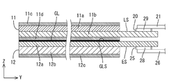
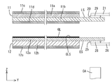
- Sectional drawing which shows schematic structure of the liquid crystal display device which concerns on Embodiment 1 of this invention.
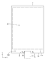
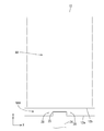
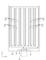
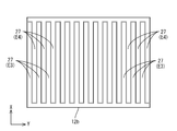
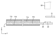
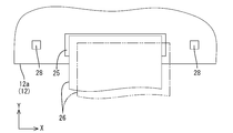
- Plan view of liquid crystal display device Cross-sectional view of liquid crystal panel and parallax barrier Plan view of a liquid crystal panel connected to a flexible substrate for panels
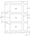
- the top view which shows the arrangement of the pixel electrode and each wiring in the array substrate which comprises a liquid crystal panel
- the top view which shows the arrangement
- the top view which shows the arrangement
- the top view which shows the arrangement
- Explanatory drawing which represents roughly the relationship between an observer's eyes, the barrier part and barrier opening part of a parallax barrier, and the pixel for right eyes and the pixel for left eyes of a liquid crystal panel
- the top view showing the positional relationship seen in the plane of a panel side index part and the flexible substrate for panels Sectional drawing which shows the state before attaching the flexible substrate for barriers with respect to a parallax barrier
- Sectional drawing which shows the state which the adhesion layer flowed out from the regular formation range, and was expanded
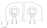
- the top view showing the positional relationship seen in the plane of an index part and a panel side index part
- FIGS. 1 A first embodiment of the present invention will be described with reference to FIGS.
- a liquid crystal display device (display device) 10 is illustrated.
- a part of each drawing shows an X axis, a Y axis, and a Z axis, and each axis direction is drawn to be a direction shown in each drawing.
- FIG. 1 is used as a reference, and the upper side of the figure is the front side and the lower side of the figure is the back side.
- the liquid crystal display device 10 is formed in a rectangular shape as viewed in plan as a whole, and is used in a portrait (vertical) or landscape (horizontal) orientation.
- a liquid crystal panel (display panel) 11 that displays an image
- a parallax barrier 12 that allows an observer to observe an image displayed on the display surface of the liquid crystal panel 11 as a stereoscopic image (3D image, three-dimensional image).
- a backlight device (illumination device) 13 that is an external light source that emits light toward the liquid crystal panel 11 and the parallax barrier 12.
- the liquid crystal display device 10 includes a bezel 14 that holds (holds) the liquid crystal panel 11 and the parallax barrier 12, and a housing 15 that is attached to the bezel 14 and accommodates the liquid crystal panel 11 and the backlight device 12.
- the liquid crystal panel 11 and the parallax barrier 12 have the main plate surfaces facing each other, the liquid crystal panel 11 is relatively on the front side (light emission side, observer side), and the parallax barrier 12 is relatively on the back side (backlight). They are arranged on the device 13 side and on the side opposite to the light emitting side) and are fixed by being fixed by a fixing layer GL interposed therebetween.
- the fixing layer GL is made of an ultraviolet curable resin material having sufficient translucency so as to be almost transparent.
- the ultraviolet curable resin material forming the fixing layer GL is applied in a liquid state to at least one of the liquid crystal panel 11 and the parallax barrier 12 that are to be fixed, and then the liquid crystal panel 11 and the parallax barrier 12 are bonded together. It is hardened by being irradiated with ultraviolet rays, and both 11 and 12 can be held in a fixed state.
- the ultraviolet curable resin material forming the fixing layer GL is, for example, a cationic polymerization type mainly composed of epoxy or vinyl ether.
- the liquid crystal display device 10 according to the present embodiment includes various information such as portable information terminals (including electronic books and PDAs), cellular phones (including smartphones), notebook computers, digital photo frames, and portable game machines.
- the screen size of the liquid crystal panel 11 constituting the liquid crystal display device 10 is about several inches to several tens of inches, such as 3.4 inches, and is generally a size classified as small or medium-sized. ing.
- the liquid crystal panel 11 will be described. As shown in FIGS. 3 and 4, the liquid crystal panel 11 is interposed between a pair of transparent (translucent) glass substrates 11 a and 11 b having a rectangular shape, and both the substrates 11 a and 11 b. And a liquid crystal layer (not shown) containing liquid crystal molecules which are substances whose optical properties change with application, and a sealing agent (not shown) in a state where both substrates 11a and 11b maintain a gap corresponding to the thickness of the liquid crystal layer. Are pasted together. As shown in FIG. 4, the liquid crystal panel 11 has a display area AA in which an image is displayed (a range surrounded by an alternate long and short dash line in FIG.
- polarizing plates 11c and 11d are attached to the outer surface sides of both substrates 11a and 11b, respectively, and the size (area) of both polarizing plates 11c and 11d depends on the display area AA. And almost the same level.
- the fixed layer GL described above is almost entirely provided on the outer surface facing the back side of the polarizing plate 11 d on the back side (parallax barrier 12 side), that is, the surface facing the parallax barrier 12. Is provided. As shown in FIG.
- the long side direction (Y-axis direction) coincides with the vertical direction (vertical direction) when viewed from the observer, and the short side direction.
- X-axis direction is the same as the horizontal direction (left-right direction, alignment direction of both eyes LE and RE) when viewed from the observer, and when used in a landscape, the long side direction is horizontal when viewed from the observer.
- the short side direction matches the vertical direction when viewed from the observer.
- the front side is the CF substrate 11a
- the back side is the array substrate 11b.
- a large number of TFTs (Thin Film Transistors) 16 and pixel electrodes 17 which are switching elements are arranged on the inner surface side (the liquid crystal layer side, the surface facing the CF substrate 11a) of the array substrate 11b, as shown in FIG. 5, a large number of TFTs (Thin Film Transistors) 16 and pixel electrodes 17 which are switching elements are arranged.
- a gate wiring 18 and a source wiring 19 having a lattice shape are disposed so as to surround the TFT 16 and the pixel electrode 17.
- Both the gate wiring 18 and the source wiring 19 are made of copper, which is a light-shielding material having conductivity (a metal material having a light-shielding property).
- the gate wiring 18 and the source wiring 19 are connected to the gate electrode and the source electrode of the TFT 16, respectively, and the pixel electrode 17 is connected to the drain electrode of the TFT 16.
- a terminal portion 20 routed from the gate wiring 18 and the source wiring 19 is formed at one end portion in the long side direction of the array substrate 11b.
- One end of the flexible substrate 21 is connected.
- the panel flexible substrate 21 is pressure-bonded to the terminal portion 20 via an anisotropic conductive film (ACF: Anisotropic Conductive Film) (not shown).
- ACF anisotropic Conductive Film
- the panel flexible board 21 is connected to a control board (not shown) at the other end, so that an image signal supplied from the control board can be transmitted to the wirings 18 and 19 of the liquid crystal panel 11. .
- Both the terminal portion 20 and the panel flexible substrate 21 are arranged in the non-display area NAA described above.
- the pixel electrode 17 is made of a light-transmitting material (substantially transparent metal material) having conductivity such as ITO (Indium Tin Oxide).
- the pixel electrodes 17 on the array substrate 11b side are overlapped with each other in a plan view.
- a large number of color filters are provided side by side.
- the color filter is arranged such that the colored portions 22 exhibiting R (red), G (green), and B (blue) are alternately arranged along the X-axis direction.
- the coloring portion 22 has a rectangular shape in plan view, and the long side direction and short side direction thereof coincide with the long side direction and short side direction of the substrates 11a and 11b, and the X-axis direction on the CF substrate 11a.
- each coloring part 22 which comprises a color filter
- the light-shielding part (black matrix) 23 which makes
- the light shielding portion 23 is arranged so as to overlap the gate wiring 18 and the source wiring 19 on the array substrate 11b side in plan view.
- one pixel PX which is a display unit, is configured by a set of three colored portions 22 of R, G, and B and three pixel electrodes 17 corresponding thereto, and the pixel PX
- a large number of substrates 11a and 11b are arranged in parallel in a matrix along the main plate surfaces, that is, the display surfaces (X-axis direction and Y-axis direction).
- a counter electrode (not shown) facing the pixel electrode 17 on the array substrate 11 b side is provided on the surface of each coloring portion 22 and the light shielding portion 23. As shown in FIG.
- the CF substrate 11a has a longer side dimension smaller than that of the array substrate 11b, and the terminal portion 20 and the flexible panel are out of both ends in the long side direction with respect to the array substrate 11b. Bonding is performed with the end opposite to the substrate 21 side aligned.
- An alignment film (not shown) for aligning liquid crystal molecules contained in the liquid crystal layer is formed on the inner surfaces of both the substrates 11a and 11b.
- the backlight device 13 will be briefly described prior to the parallax barrier 12.
- the backlight device 13 is a so-called edge light type (side light type), and has a light source, a substantially box-shaped chassis that opens on the front side (the liquid crystal panel 11 side, the light emission side) and accommodates the light source, and a light source.
- a light guide member that is arranged opposite to the end portion, guides light from the light source, and emits the light toward the opening portion of the chassis, and an optical member arranged to cover the opening portion of the chassis.
- the light emitted from the light source is incident on the end of the light guide member, then propagates through the light guide member and is emitted toward the opening of the chassis, and then the in-plane luminance distribution is uniform by the optical member.
- the liquid crystal panel 11 is irradiated after being converted into planar light.
- the light transmittance with respect to the liquid crystal panel 11 is selectively controlled within the surface of the display surface by driving the TFT 16 included in the liquid crystal panel 11, whereby a predetermined image can be displayed on the display surface.
- Detailed illustrations of the light source, chassis, light guide member, and optical member are omitted.
- the parallax barrier 12 is interposed between a pair of transparent (translucent) glass substrates 12a and 12b having a rectangular shape, and both the substrates 12a and 12b. And a liquid crystal layer (not shown) containing liquid crystal molecules, which are substances whose optical characteristics change with application, and a sealing agent (not shown) in a state where both substrates 12a and 12b maintain a gap corresponding to the thickness of the liquid crystal layer.
- a so-called liquid crystal panel The parallax barrier 12 has substantially the same screen size as the liquid crystal panel 11 and is bonded to the fixing layer GL in a posture parallel to the liquid crystal panel 11.
- the parallax barrier 12 When used in a portrait, the parallax barrier 12 has a long side direction (Y axis Direction) matches the vertical direction (vertical direction) as viewed from the observer, and the short side direction (X-axis direction) matches the horizontal direction (left-right direction, alignment direction of both eyes LE, RE) as viewed from the observer.
- the long side direction coincides with the horizontal direction when viewed from the observer
- the short side direction coincides with the vertical direction when viewed from the observer.
- the fixed layer GL described above is formed on the outer surface facing the front side of the first substrate 12a on the front side (liquid crystal panel 11 side), that is, the surface facing the liquid crystal panel 11, in the display area AA.
- a polarizing plate 12c is attached to the outer surface (back surface) side of the second substrate 12b arranged on the back side.
- the parallax barrier 12 can control the alignment state of the liquid crystal molecules and the light transmittance according to the voltage applied to the liquid crystal layer, thereby forming a barrier unit BA, which will be described in detail later.
- the image displayed on the pixel PX of the liquid crystal panel 11 can be separated by parallax so that the observer can observe it as a stereoscopic image.
- the parallax barrier 12 actively controls the light transmittance of the liquid crystal layer to display a planar image (2D image, two-dimensional image) and a stereoscopic image (3D image, three-dimensional image) on the display surface of the liquid crystal panel 11. It can be said that this is a switching liquid crystal panel that can be switched and displayed.
- a translucent material having conductivity As shown in FIG. 8, on the inner surface side (the liquid crystal layer side, the surface facing the second substrate 12b) of the first substrate 12a on the front side that constitutes the parallax barrier 12, a translucent material having conductivity (almost) A plurality of transparent electrode portions 24 made of ITO, which is a transparent metal material, are provided in parallel.
- the transparent electrode portion 24 has a stripe shape (band shape) having a substantially constant width extending along the long side direction (Y-axis direction) of the first substrate 12a and the short side direction (X-axis direction) of the first substrate 12a. ) Are arranged in parallel at a predetermined interval.
- the transparent electrode portions 24 are grouped into two groups, and those constituting the first electrode E1 described below and those constituting the second electrode E2 are alternately arranged. Specifically, among the multiple transparent electrode portions 24 arranged in parallel along the X-axis direction, for example, odd-numbered one ends are connected to each other to form a comb-shaped first electrode E1. On the other hand, by connecting the other ends of the even-numbered ones to each other, a second electrode E2 having a comb-like shape is formed so as to mesh with the first electrode E1. A terminal portion 25 led from the first electrode E1 and the second electrode E2 (transparent electrode portion 24) is formed at one end portion in the long side direction of the first substrate 12a. One end side of the barrier flexible substrate 26 is connected.
- the barrier flexible substrate 26 is crimped to the terminal portion 25 via an anisotropic conductive film (not shown).
- the barrier flexible board 26 is connected to a control board (not shown) at the other end, so that a barrier drive signal supplied from the control board can be transmitted to the first electrode E1 and the second electrode E2. Yes.
- the terminal portion 25 and the barrier flexible substrate 26 are arranged in a region of the parallax barrier 12 that overlaps the non-display region NAA in the liquid crystal panel 11.
- an area of the parallax barrier 12 that overlaps the display area AA of the liquid crystal panel 11 is surrounded by a two-dot chain line.
- the first substrate side 12a On the other hand, on the inner surface side (the liquid crystal layer side, the surface facing the first substrate 12a) of the second substrate 12b on the back side constituting the parallax barrier 12, as shown in FIG. 9, the first substrate side 12a. Similarly, a plurality of transparent electrode portions 27 made of ITO are provided in parallel.
- the transparent electrode portion 27 has a stripe shape (band shape) with a substantially constant width extending along the short side direction (X-axis direction) of the second substrate 12b, and the long side direction (Y-axis direction) of the second substrate 12b. ) Are arranged in parallel at a predetermined interval. That is, the transparent electrode portion 27 included in the second substrate 12b has its extending direction and parallel direction orthogonal to the extending direction and parallel direction (see FIG.
- the transparent electrode portions 27 included in the second substrate 12b are grouped into two, and those constituting the third electrode E3 described below and those constituting the fourth electrode E4 are alternately arranged.
- a fourth electrode E4 having a comb shape is formed so as to mesh with the third electrode E3.
- the parallax barrier 12 for example, when the potential difference between the first electrode E1 and the second electrode E2 facing each other and the third electrode E3 and the fourth electrode E4 is zero, the light transmission of the liquid crystal layer It is possible to use a so-called normally white mode switching liquid crystal panel which has a maximum rate and can transmit light over the entire region to the maximum.
- the parallax barrier 12 according to this embodiment is controlled in its drive by supplying a predetermined alternating voltage to each of the electrodes E1 to E4, and is used in a portrait and in a landscape. In both cases, it is possible to make the observer observe a stereoscopic image.
- the liquid crystal display device 10 when the liquid crystal display device 10 is used in a portrait, for example, the potential difference between the second electrode E2, the third electrode E3, and the fourth electrode E4 does not occur, but the first electrode An AC voltage is supplied to each of the electrodes E1 to E4 so that a potential difference is generated between E1, the third electrode E3, and the fourth electrode E4. Then, as shown in FIG. 10, in the liquid crystal layer in the parallax barrier 12, the light transmittance of a region overlapping the first electrode E1 in a plan view is minimized, and a barrier portion BA that blocks light is formed here. On the other hand, the light transmittance of the region overlapping the second electrode E2 in plan view is maximized, and a barrier opening BO that transmits light is formed here.
- Both the barrier portion BA and the barrier opening BO are formed in stripes extending along the Y-axis direction, like the transparent electrode portions 24, and are arranged in a plurality alternately in parallel along the X-axis direction.
- the alignment direction of the barrier portion BA and the barrier opening BO coincides with the alignment direction (X-axis direction) of both eyes LE and RE of the observer when used in the portrait.
- the drive is controlled so that the left-eye image and the right-eye image are alternately displayed on the pixels PX arranged in the axial direction
- the displayed right-eye image (right-eye pixel RPX) and left-eye image (left-eye pixel) LPX) is observed by the barrier portion BA, and the observation angle is controlled separately by the observer's right eye RE and left eye LE through the barrier opening BO.
- the binocular parallax effect can be obtained and the observer can observe a stereoscopic image when used in a portrait.
- the liquid crystal display device 10 when the liquid crystal display device 10 is used in a landscape, for example, there is no potential difference between the first electrode E1, the second electrode E2, and the fourth electrode E4, but the first electrode E1 and the first electrode E1.
- An AC voltage is supplied to each of the electrodes E1 to E4 so that a potential difference is generated between the two electrodes E2 and the third electrode E3.
- the light transmittance of the region overlapping the third electrode E3 in plan view is minimized, and the barrier portion BA that blocks light is formed here, whereas the fourth electrode E4 And the barrier opening BO through which light is transmitted is maximized in the region that overlaps in plan view.
- Both the barrier portion BA and the barrier opening BO are formed in stripes extending along the X-axis direction, like the transparent electrode portions 27, and are arranged in a plurality alternately in parallel along the Y-axis direction.
- the alignment direction of the barrier portion BA and the barrier opening BO coincides with the alignment direction of the observer's eyes LE and RE (Y-axis direction in parentheses in FIG. 10) when used in the landscape.
- the display When the drive is controlled so that the left-eye image and the right-eye image are alternately displayed on the pixels PX arranged in the Y-axis direction in the liquid crystal panel 11 in the state, the displayed right-eye image (right-eye pixel RPX) and The left-eye image (left-eye pixel LPX) is observed by being separated into the observer's right eye RE and left eye LE, respectively, through the barrier opening BO, while the observation angle is regulated by the barrier section BA. Accordingly, a binocular parallax effect can be obtained when used in a landscape, and an observer can observe a stereoscopic image.
- the liquid crystal display device 10 capable of stereoscopic display both when used in portrait and when used in landscape includes a gyro sensor (not shown) and the orientation of the liquid crystal display device 10 by the gyro sensor. (Whether it is a portrait or a landscape), and the driving of the liquid crystal panel 11 and the parallax barrier 12 is automatically switched between the portrait mode and the landscape mode based on the detection signal. Is more preferable. Further, when the observer observes a planar image, each of the electrodes E1 to E4 is set so that no potential difference is generated between the first electrode E1 and the second electrode E2, and the third electrode E3 and the fourth electrode E4.
- the parallax barrier 12 is not formed with the barrier portion BA that blocks light. Therefore, parallax does not occur in the image displayed on each pixel PX of the liquid crystal panel 11, and thus the observer can observe a planar image (2D image, two-dimensional image).
- the liquid crystal panel 11 having the above-described configuration and the parallax barrier 12 are bonded together using the fixing layer GL, the liquid crystal panel 11 and the parallax barrier 12 are aligned along the display surface (X-axis direction and Y-axis direction). ) Is required to be accurately aligned.
- the positions of the right-eye pixel RPX and the left-eye pixel LPX, the barrier unit BA, and the barrier opening BO Since the relation is out of order, for example, the right-eye pixel RPX is observed by the left eye LE of the observer, or conversely, the left-eye pixel LPX is observed by the right eye RE, so that a problem of so-called crosstalk (double reflection) occurs. This is because it may become apparent and display quality may be significantly impaired.
- the parallax barrier 12 and the liquid crystal panel 11 include an index section (index serving as an index for aligning the liquid crystal panel 11 and the parallax barrier 12 in the direction along the display surface).
- a barrier-side mark 28 and a panel-side indicator portion (panel-side mark) 29 are provided.
- the indicator unit 28 is arranged in a region of the first substrate 12 a that configures the parallax barrier 12 and overlaps with the non-display region NAA in the liquid crystal panel 11, and the terminal
- a pair of terminal portions 25 is provided at a side position of the portion 25 so as to sandwich the terminal portion 25, and each has a substantially square shape when viewed in plan.
- the pair of indicator portions 28 are arranged so that the distances between the pair of indicator portions 28 are substantially equal to each other and are symmetrical with respect to the X-axis direction.
- the indicator portion 28 is made of the same material as the transparent electrode portion 24 provided on the first substrate 12a, that is, ITO, which is a translucent material having conductivity. Thereby, in the process of patterning the transparent electrode part 24 on the first substrate 12a in the process of manufacturing the parallax barrier 12, the indicator part 28 can be patterned simultaneously with the transparent electrode part 24, thereby reducing the manufacturing cost. It is supposed to contribute.
- the index portion 28 is substantially transparent, but when captured by the positioning camera CA (FIGS. 15 and 17), a contour (outer peripheral edge) forming a substantially square frame shape is captured. As a result, the index portion 28 can be identified and its position information can be acquired.
- the indicator portion 28 having a substantially square shape has a side of, for example, about 150 ⁇ m.
- the panel-side index portion 29 is arranged in the non-display area NAA in the array substrate 11 b constituting the liquid crystal panel 11 and at a side position of the terminal portion 20.
- a pair of terminals 20 are provided so as to sandwich the terminal portion 20, and each has a substantially annular shape when seen in a plan view.
- the outer peripheral edge has a circular shape
- the inner peripheral edge has a substantially square shape.
- the inner peripheral edge of the panel-side indicator portion 29 having a substantially square shape has one side larger than the side of the indicator portion 28, for example, about 200 ⁇ m.
- the inner peripheral edge of the panel-side indicator portion 29 is similar to the indicator portion 28 and can surround the indicator portion 28 over the entire circumference. Therefore, when the panel-side indicator portion 29 and the indicator portion 28 are arranged concentrically with each other, the distance between the outer peripheral edge of the indicator portion 28 and the inner peripheral edge of the panel-side indicator portion 29 is constant over the entire circumference (for example, 25 ⁇ m). Degree) (FIG. 18). In this state, a region between the outer peripheral edge of the indicator portion 28 and the inner peripheral edge of the panel-side indicator portion 29 has a regular rectangular frame shape.
- the pair of panel side indicator portions 29 are arranged so that the distances between the pair of panel side indicator portions 29 are substantially equal to each other and are symmetrical with respect to the X-axis direction.
- the panel-side index portion 29 is made of copper, which is a light-shielding material having conductivity, that is, the same material as the gate wiring 18 and the source wiring 19 provided on the array substrate 11b. Accordingly, in the process of patterning the gate wiring 18 or the source wiring 19 on the array substrate 11b in the manufacturing process of the liquid crystal panel 11, the panel-side indicator portion 29 can be patterned simultaneously with the gate wiring 18 or the source wiring 19. Therefore, it is considered that it contributes to reduction of manufacturing cost.
- the index part 28 is made of a light-transmitting material, and therefore the following problems may occur. That is, in the step of bonding the liquid crystal panel 11 and the parallax barrier 12, the ultraviolet curable resin material of the fixing layer GL that has been in a liquid state before curing has a normal formation range (approximately the same as the display area AA and the polarizing plate 11d). If the ultraviolet curable resin material adheres to the indicator portion 28, the contour image of the indicator portion 28 obtained by imaging with the camera CA may not be a square.
- the index unit 28 cannot be identified and an error occurs in the bonding apparatus and its operation stops, or the position information of the index unit 28 cannot be acquired normally and the position of the index unit 28 is incorrect.
- the liquid crystal panel 11 and the parallax barrier 12 are pasted together in a state of being misaligned. If the operation of the bonding apparatus is stopped, production efficiency may be reduced and manufacturing costs may be increased. Further, if the liquid crystal panel 11 and the parallax barrier 12 are bonded together with their positions shifted, crosstalk is likely to occur as described above, and the display quality may be degraded.
- the indicator portion 28 is opposite to the surface facing the liquid crystal panel 11 in the parallax barrier 12, that is, the formation surface GLS of the fixed layer GL, as shown in FIG. It is provided on the side surface ES.
- the indicator portion 28 is provided on the inner surface, which is the same surface of the first substrate 12a, in the same process as the transparent electrode portion 24.
- the fixing layer GL is provided on the outer surface of the first substrate 12a facing the liquid crystal panel 11. Therefore, the formation surface ES of the transparent electrode portion 24 and the indicator portion 28 in the first substrate 12a is a surface facing the opposite side to the formation surface GLS of the fixed layer GL.
- the ultraviolet curable resin material of the fixing layer GL in a liquid state before curing is Even when it flows out of the normal formation range, it is assumed that it stays in the plane of the formation surface GLS and hardly reaches the formation surface ES on the opposite side. Therefore, the situation in which the ultraviolet curable resin material of the fixing layer GL adheres to the indicator portion 28 is prevented.
- the panel-side index portion 29 is provided on the surface of the liquid crystal panel 11 that faces the parallax barrier 12, that is, the surface LS opposite to the surface on which the fixing layer GL is formed. Specifically, the panel-side index portion 29 is provided on the inner surface that is the same material as the gate wiring 18 or the source wiring 19 and is the same surface of the array substrate 11b in the same process.
- the fixing layer GL is provided on the outer surface facing the parallax barrier 12 in the polarizing plate 11d attached to the outer surface of the array substrate 11b. Therefore, the formation surface LS of the gate wiring 18, the source wiring 19, and the panel side indicator portion 29 on the array substrate 11 b is a surface facing the opposite side to the formation surface of the fixed layer GL.
- the panel-side index portion 29 and the fixing layer GL have a back-to-back positional relationship across the array substrate 11b and the polarizing plate 11d, so that the ultraviolet curing of the fixing layer GL in a liquid state before curing is performed. Even when the conductive resin material flows out of the regular formation range, it remains within the formation surface and hardly reaches the formation surface LS on the opposite side. This prevents the ultraviolet curable resin material of the fixing layer GL from adhering to the panel side indicator portion 29.
- the backlight device 13 is housed in a housing 15, and a liquid crystal panel 11 and a parallax barrier 12 that are separately manufactured are combined and integrated to form a bezel 14 and a housing 15. Manufactured by holding between.
- the liquid crystal panel 11 and the parallax barrier 12 are assumed to be subjected to a process of attaching the corresponding flexible substrates 21 and 26 prior to the mutual bonding process, which will be described first.
- the liquid crystal panel 11 is placed on a work table that constitutes the apparatus for attaching the panel flexible substrate 21, and as shown in FIG. 13, both the terminal portion 20 and the panel-side index portion 29 are set to face upward.
- An anisotropic conductive film is attached to the surface of the terminal portion 20 in advance.
- the panel flexible substrate 21 is disposed above the terminal portion 20 so as to face the terminal portion 20, and the terminal portion 20, the panel flexible substrate 21 and the panel-side index portion 29 are imaged by the camera CA disposed further upward.
- the X-axis direction of the panel flexible substrate 21 is different from And the position about the Y-axis direction is adjusted.
- the positional relationship between the panel flexible substrate 21 and the pair of panel side indicator portions 29 is the same, that is, the position indicated by the solid line in FIG. It adheres via an anisotropic conductive film. Accordingly, the panel flexible substrate 21 is connected to the terminal portion 20 at a regular position.
- the parallax barrier 12 is placed on a work table that constitutes the attachment device for the flexible substrate for barrier 26, and as shown in FIG. 15, both the terminal portion 25 and the indicator portion 28 face upward.
- An anisotropic conductive film is attached in advance to the surface of the terminal portion 25.
- the barrier flexible substrate 26 is disposed in an opposing manner above the terminal portion 25, and the terminal portion 25, the barrier flexible substrate 26, and the index portion 28 are imaged by the camera CA disposed further upward.
- the terminal portion 25 is arranged to be sandwiched between the pair of indicator portions 28, so that the position of the barrier flexible substrate 26 with respect to the terminal portion 25 is accurately and reliably detected by the pair of indicator portions 28. Can do.
- the positional relationship between one index portion 28 and the barrier flexible substrate 26 is different from the positional relationship between the other index portion 28 and the barrier flexible substrate 26.
- the barrier flexible substrate 26 Since the barrier flexible substrate 26 is displaced with respect to the terminal portion 25 in at least one of the X-axis direction and the Y-axis direction, the barrier flexible substrate 26 has the X-axis direction and the Y-axis direction. Adjust the position about. When the positional relationship between the barrier flexible substrate 26 and the pair of indicator portions 28 is the same, that is, the position indicated by the solid line in FIG. 16, the barrier flexible substrate 26 is anisotropic with respect to the terminal portion 25. It sticks through a conductive film. Accordingly, the barrier flexible substrate 26 is connected to the terminal portion 25 at a normal position.
- the parallax barrier 12 is placed on the work table constituting the bonding apparatus, and as shown in FIG. 17, the outer surface of the first substrate 12a (the formation surface GLS of the fixing layer GL) faces upward, and the terminal portion 25 and the index It is assumed that the portion 28 faces downward.
- the outer surface of the first substrate 12 a in the parallax barrier 12 is preliminarily coated with an ultraviolet curable resin material of the fixed layer GL in a liquid state. In this state, the liquid crystal panel 11 is disposed above the parallax barrier 12 so as to face each other.
- the liquid crystal panel 11 has a posture in which the terminal portion 25 and the indicator portion 28 face upward, and the outer surface of the polarizing plate 11d (formation surface of the fixing layer GL) faces the lower side, that is, the liquid crystal panel 11 side.
- the index unit 28 and the panel-side index unit 29 are imaged by the camera CA disposed below the parallax barrier 12.
- the panel-side index portion 29 is made of a light-shielding material, and thus can be imaged by the camera CA through both the substantially transparent array substrate 11b and the first substrate 12a.
- the index part 28 and the panel-side index part 29 are imaged by the camera CA, an image is obtained in which the index part 28 exists inside the panel-side index part 29 that is annular and slightly larger than the index part 28.
- the interval held between the outer peripheral edge of the indicator portion 28 and the inner peripheral edge of the panel-side indicator portion 29 is not constant over the entire circumference.
- the liquid crystal panel 11 and the parallax barrier 12 are displaced in at least one of the X-axis direction and the Y-axis direction. And the parallax barrier 12 are adjusted in the X-axis direction and the Y-axis direction. As shown in FIG.
- the indicator portion 28 and the panel-side indicator portion 29 are concentric, and the interval held between the outer peripheral edge of the indicator portion 28 and the inner peripheral edge of the panel-side indicator portion 29 extends over the entire circumference.
- the liquid crystal panel 11 is fixed to the parallax barrier 12 via the fixing layer GL.
- the liquid crystal panel 11 and the parallax barrier 12 are bonded together in an accurately aligned state.
- the ultraviolet curable resin material of the fixing layer GL applied to the outer surface of the first substrate 12a in the parallax barrier 12 and in a liquid state can flow in the plane of the formation surface GLS.
- the liquid may flow out from the regular formation range (substantially the same range as the display area AA).
- the indicator portion 28 is provided on the inner surface of the first substrate 12a, that is, the surface ES opposite to the formation surface GLS of the fixing layer GL, and the fixing layer GL is back-to-back with the first substrate 12a interposed therebetween. Therefore, there is almost no situation in which the UV curable resin material of the fixed layer GL that has flowed reaches the formation surface ES of the indicator portion 28.
- the operating rate of the laminating apparatus that is, the production efficiency can be increased, manufacturing at a low cost is possible, and the display image is displayed by the parallax barrier 12 accurately aligned with the liquid crystal panel 11. Can be accurately separated and observed by an observer, and the display quality can be improved.
- the indicator portion 28 and the panel-side indicator portion 29 are provided in pairs, the relative positional relationship between the liquid crystal panel 11 and the parallax barrier 12 can be detected more accurately and reliably. It is supposed to be possible.
- the liquid crystal display device (display device) 10 is disposed opposite to the liquid crystal panel (display panel) 11 having a display surface capable of displaying an image, and the liquid crystal panel 11.
- 11 displays a parallax barrier 12 capable of separating an image displayed on the screen 11 by parallax, a fixing layer GL for fixing opposing surfaces of the liquid crystal panel 11 and the parallax barrier 12, and the liquid crystal panel 11 and the parallax barrier 12.
- An index portion 28 is provided as an index for alignment in the direction along the surface, and is disposed on the surface ES of the parallax barrier 12 opposite to the formation surface GLS of the fixed layer GL.
- the liquid crystal panel 11 and the parallax barrier 12 are bonded to each other while facing each other, the liquid crystal panel 11 and the parallax barrier 12 are positioned in the direction along the display surface by using the index unit 28 as an index.
- the index unit 28 is disposed on the surface ES of the parallax barrier 12 on the side opposite to the formation surface GLS of the fixed layer GL, a situation occurs in which the fixed layer GL is directly attached to the index portion 28. Can be prevented. Therefore, it is difficult to identify the index portion 28 as an index due to the fixed layer GL, or the position of the index portion 28 is erroneously detected, and the index portion 28 is easily identified as an index.
- the position of the index unit 28 can be detected accurately. Since it becomes easy to identify the index part 28 as an index, the certainty of alignment can be increased and the production efficiency can be improved, which is suitable for reducing the manufacturing cost. Further, since the position of the index unit 28 can be accurately detected, the alignment between the liquid crystal panel 11 and the parallax barrier 12 can be performed with high accuracy, and thus the function of the parallax barrier 12, that is, the liquid crystal panel 11. It is possible to more reliably exhibit the function of separating images displayed on the screen by parallax, and the display quality is excellent.
- the indicator portion 28 is made of a translucent material. In this way, if the fixing layer GL is attached to the indicator portion 28 made of a translucent material, the above-described problem is more likely to occur, but the indicator portion 28 is included in the fixing layer GL in the parallax barrier 12. Since the situation where the fixed layer GL adheres to the indicator portion 28 is prevented by being arranged on the surface opposite to the formation surface GLS, it is extremely useful.
- the parallax barrier 12 is provided with a transparent electrode portion 24 made of a light-transmitting material having conductivity, and the index portion 28 is made of the light-transmitting material having conductivity described above.
- the indicator portion 28 can be provided in the step of providing the transparent electrode portion 24. Therefore, the manufacturing cost related to the parallax barrier 12 can be reduced.
- the above-described translucent material having conductivity is ITO (Indium Tin Oxide).
- ITO Indium Tin Oxide
- the resistivity is low as compared with the case where ZnO (Zinc Oxide: zinc oxide) is used, and it is excellent in heat resistance, acid resistance, alkali resistance and the like.
- the liquid crystal panel 11 has a display area AA for displaying an image and a non-display area NAA in which no image is displayed, whereas the fixing layer GL is at least viewed in plan with the display area AA. It is formed in the overlapping range, and the indicator part 28 is arranged at a position in the parallax barrier 12 that overlaps with the non-display area NAA in a plan view. In this way, if the fixed layer GL stays in a range where it overlaps with the display area AA in a plane, the indicator portion 28 is arranged at a position that does not overlap with the fixed layer GL in a plane. Therefore, it becomes easy to identify the index unit 28 as an index, and the position can be accurately detected.
- the transparent electrode portion 24 is provided in a region that overlaps the display area AA when viewed in a plane, whereas the non-display area NAA overlaps when viewed in a plane.
- a barrier flexible substrate (barrier connection component) 26 connected to the transparent electrode portion 24 is attached, and the indicator portion 28 is disposed at a side position of the barrier flexible substrate 26.
- the indicator 28 can be used as an indicator for aligning the parallax barrier 12 and the barrier flexible substrate 26 in the direction along the display surface.
- the index unit 28 may have a function as an index for aligning the parallax barrier 12 and the barrier flexible substrate 26 in addition to a function as an index for aligning the liquid crystal panel 11 and the parallax barrier 12. Therefore, the configuration can be simplified as compared with the case where two dedicated indicator portions are provided.
- a pair of indicator portions 28 are arranged so as to sandwich the barrier flexible substrate 26 therebetween. In this way, the parallax barrier 12 and the barrier flexible substrate 26 can be more accurately and reliably aligned by the pair of indicator portions 28 arranged so as to sandwich the barrier flexible substrate 26.
- the liquid crystal panel 11 is provided with a panel side index portion 29 capable of aligning the liquid crystal panel 11 and the parallax barrier 12 based on the positional relationship in the direction along the display surface with respect to the index portion 28. In this way, the liquid crystal panel 11 and the parallax barrier 12 can be more accurately and reliably aligned by the relative positional relationship between the index portion 28 and the panel-side index portion 29.
- the panel side indicator portion 29 is disposed on the surface LS on the opposite side of the liquid crystal panel 11 from the surface on which the fixing layer GL is formed. In this way, the adhesion of the fixing layer GL to the indicator portion 28 and the panel side indicator portion 29 can be surely prevented, so that both the indicator portion 28 and the panel side indicator portion 29 can be easily identified as indicators. Both positions can be detected more accurately and reliably.
- the panel side indicator portion 29 is made of a light shielding material. This makes it easier to identify the panel-side index portion 29 as an index even when the fixing layer GL adheres to the panel-side index portion 29, as compared with the case where the panel-side index portion is made of a transparent material. The position can be detected accurately.
- the liquid crystal panel 11 is provided with a pixel PX for displaying an image and a gate wiring 18 and a source wiring 19 (wiring portion) that are connected to the pixel PX and are made of a light-shielding material having conductivity.
- the panel-side index portion 29 is made of the above-described light-shielding material having conductivity. In this way, in the process of manufacturing the liquid crystal panel 11, it is possible to provide the panel-side index portion 29 in the process of providing the gate wiring 18 and the source wiring 19. Therefore, the manufacturing cost related to the liquid crystal panel 11 can be reduced.
- the panel side indicator portion 29 has an annular shape that can surround the indicator portion 28 in a plan view. According to this configuration, the liquid crystal panel 11 and the parallax barrier 12 are more accurately and reliably positioned based on the positional relationship between the outer peripheral edge of the index portion 28 and the inner peripheral edge of the panel-side index portion 29 surrounding the periphery. Can be combined.
- the panel side indicator portion 29 is formed so that the inner peripheral edge thereof is similar to the outer peripheral edge of the indicator portion 28. In this way, when the indicator portion 28 and the panel side indicator portion 29 are in concentric positions, the distance between the outer peripheral edge of the indicator portion 28 and the inner peripheral edge of the panel side indicator portion 29 is constant over the entire circumference. Become. If this state is used as a reference for the alignment state, it is possible to detect more accurately and reliably if there is a positional deviation.
- the liquid crystal panel 11 is provided with a pixel PX for displaying an image, a gate wiring 18 and a source wiring 19 connected to the pixel PX, and a panel flexible substrate (panel) connected to the gate wiring 18 and the source wiring 19.
- the connecting part 21 is attached, and the panel-side index portion 29 is disposed at a side position of the panel flexible substrate 21.
- the panel-side index portion 29 can be used as an index for aligning the liquid crystal panel 11 and the panel flexible substrate 21 in the direction along the display surface. That is, the panel-side index unit 29 has a function as an index for aligning the liquid crystal panel 11 and the panel flexible substrate 21 in addition to a function as an index for aligning the liquid crystal panel 11 and the parallax barrier 12. Therefore, the configuration can be simplified as compared with the case where two dedicated panel-side index portions are provided.
- a pair of panel side indicator portions 29 are arranged so as to sandwich the panel flexible substrate 21.
- the liquid crystal panel 11 and the panel flexible substrate 21 can be more accurately and reliably aligned by the pair of panel side indicator portions 29 arranged so as to sandwich the panel flexible substrate 21. .
- the fixing layer GL is made of a photocurable resin material that is cured by light irradiation. If it does in this way, since it is a one-component type, it is excellent in handling and excellent in fast curability.
- the parallax barrier 112 is arranged so as to be stacked on the front side (light emitting side, observer side) with respect to the liquid crystal panel 111.
- the fixing layer GL is arranged between the polarizing plate 111c attached to the outer surface of the CF substrate 111a constituting the liquid crystal panel 111 and the first substrate 112a constituting the parallax barrier 112.
- the terminal portion 125 and the panel side indicator portion 129 included in the liquid crystal panel 111 are provided on the surface of the array substrate 111b on the fixed layer GL side. Therefore, in the bonding step, when the ultraviolet curable resin material of the fixing layer GL in a liquid state flows out from the normal formation range, as shown in FIG.
- the panel side indicator portion 129 is made of the same light-shielding material as the wirings 18 and 19 (see FIG. 5), even if a substantially transparent ultraviolet curable resin material adheres, the panel CA is identified by the camera CA. Is not often disturbed, and it is difficult to cause identification failure or misalignment.
- a protection unit 30 for protecting the index unit 28 is provided in the parallax barrier 212.
- action, and effect as above-mentioned Embodiment 1 is abbreviate
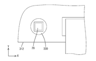
- the first substrate 212a that forms the parallax barrier 212 is provided with a protective portion 30 that is opposed to the outer edge of the indicator portion 28.
- the protection part 30 is provided on the formation surface of the index part 28 in the first substrate 212a, and has an annular shape surrounding the index part 28 over the entire circumference.
- the protection unit 30 has a similar shape to the index unit 28 in a plan view, and has a substantially square frame shape.
- the protection unit 30 is made of the same material as the index unit 28, that is, ITO. Accordingly, the protection unit 30 is patterned at the same time as the step of patterning the transparent electrode unit 24 (see FIG. 8) and the indicator unit 28 on the first substrate 212a in the manufacturing process of the parallax barrier 212. Yes.
- the alignment film for aligning the liquid crystal has substantially the same range as the transparent electrode portion 24 (display). Region AA).
- This alignment film is made of polyimide, which is a substantially transparent material, and is formed so as to be laminated on the transparent electrode portion 24 formed on the inner surface of the first substrate 212a, and then the surface is rubbed. In this rubbing treatment, since the surface of the alignment film is rubbed with the cloth, a minute wrinkle PIR (indicated by a two-dot chain line in FIG. 23) is generated from the surface of the alignment film.
- the protective portion 30 is provided so as to surround the indicator portion 28, so that the wrinkles PIR of the alignment film adhere to the outer edge of the protective portion 30, but adhere to the indicator portion 28. Can be prevented. Thereby, it is possible to prevent the occurrence of identification failure or alignment failure in the bonding step.
- the parallax barrier 212 includes the pair of substrates 212a and 212b facing each other, the liquid crystal sealed between the pair of substrates 212a and 212b, and the pair of substrates 212a and 212b.
- Each of the pair of substrates 212a and 212b is fixed to the liquid crystal panel 11 through the fixing layer GL.
- an indicator portion 28 is provided, and further, a protective portion 30 that is opposed to the outer edge of the indicator portion 28 is provided. In this way, if the protective portion 30 that is opposed to the outer edge of the indicator portion 28 is provided, a small alignment film wrinkle PIR occurs when the alignment film is provided on one substrate 212a. However, it is possible to prevent the soot PIR from adhering directly to the indicator portion 28.
- the protection part 30 has an annular shape surrounding the indicator part 28 over the entire circumference. In this way, it is possible to more reliably prevent the alignment film wrinkles PIR from adhering to the indicator portion 28.
- the protective portion 30 is formed so that the inner peripheral edge thereof is similar to the outer peripheral edge of the indicator portion 28. In this way, it is possible to reduce the possibility that the protection unit 30 becomes an obstacle to identifying the index unit 28, and thus it is possible to perform alignment more accurately and reliably.
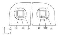
- Embodiment 4 A fourth embodiment of the present invention will be described with reference to FIG. 24 or FIG. In this Embodiment 4, what changed the shape of the protection part 330 shown in above-mentioned Embodiment 3 is shown. In addition, the overlapping description about the same structure, effect
- the outer peripheral edge has a circular shape, whereas the inner peripheral edge has a substantially square shape. That is, the protective portion 330 has an inner peripheral edge similar to the outer peripheral edge of the indicator portion 28 and the inner peripheral edge of the panel side indicator portion 29, whereas the outer peripheral edge is similar to the outer peripheral edge of the panel side indicator portion 29. I am doing. And since this protection part 330 is made into the same shape as the panel side parameter
- the liquid crystal panel 11 has a panel side on which the liquid crystal panel 11 and the parallax barrier 12 can be aligned based on the positional relationship with respect to the indicator portion 28 in the direction along the display surface.
- the indicator part 29 is provided, and the protection part 330 is formed so that at least one of the outer peripheral edges and the inner peripheral edges of the panel side indicator part 29 is similar.
- the liquid crystal panel 11 and the parallax barrier 12 are aligned by the positional relationship between the protection unit 330 and the panel side index unit 29 in addition to the positional relationship between the index unit 28 and the panel side index unit 29.
- the alignment can be performed with high accuracy.
- the protection part 330 has the same shape as the panel side index part 29 in a plan view. In this way, when the protection part 330 and the panel-side index part 29 are in concentric positions, the inner and outer peripheral edges of the protection part 330 and the panel-side index part 29 are in agreement with each other. If this state is used as a reference for the alignment state, it is possible to more accurately and reliably detect a misalignment.
- the indicator portion has a square shape and the panel side indicator portion has an annular shape surrounding the indicator portion.
- the panel side indicator portion has a square shape. It is also possible that the indicator portion has an annular shape surrounding the panel side indicator portion.
- the indicator portion has a square shape when viewed in a plane.
- other shapes such as a circle, an ellipse, a triangle, a rectangle, a rhombus, a trapezoid, and a pentagon or more It is also possible to change to.
- the inner peripheral edge of the panel-side index portion is illustrated as a square when viewed in plan, but other shapes such as a circle, an ellipse, a triangle, a rectangle, a rhombus, a trapezoid, It is also possible to change to a pentagon or more polygon.
- the outer peripheral edge of the panel-side index portion is exemplified as a circular shape when viewed in plan, but other shapes such as an ellipse, a triangle, a square, a rectangle, a rhombus, a trapezoid, It is also possible to change to a pentagon or more polygon.
- the outer peripheral edge of the protection portion is illustrated as a square or a circle when viewed in plan, but other shapes such as an ellipse, a triangle, a rectangle, a rhombus, and a trapezoid are illustrated. It is also possible to change to a polygon of pentagon or more.
- the shape of the inner peripheral edge of the protection portion can be changed to, for example, a circle, an ellipse, a triangle, a rectangle, a rhombus, a trapezoid, or a pentagon or more polygon.
- the protective part has the same shape as the panel-side index part.
- the inner peripheral edge of the protective part and the panel-side index part have the same shape, and the outer peripheral edge is the same.
- Those having different shapes are also included in the present invention. Contrary to this, it is of course possible that the outer peripheral edges of the protective part and the panel side indicator part have the same shape, and the inner peripheral edges have different shapes.
- the indicator portion surrounded by the panel-side indicator portion is shown as being solid.
- the indicator portion surrounded by the panel-side indicator portion is formed in a hollow shape (annular).
- the panel-side indicator portion has an endless annular shape that is not interrupted over the entire circumference.
- a C-shaped or U-shaped end-shaped annular shape is also possible. It is.
- index part similarly to the above.
- the parallax barrier is arranged on the front side and the liquid crystal panel is arranged on the back side in Embodiment 2 described above, the panel side index portion is exemplified on the surface on the fixing layer side in the liquid crystal panel.
- the parallax barrier is disposed on the back side and the liquid crystal panel is disposed on the front side, and the panel side index portion is provided on the surface of the liquid crystal panel on the fixed layer side.
- the index unit and the panel side index unit are arranged at the side positions of the respective terminal units in the liquid crystal panel and the parallax barrier.
- the arrangement of the panel side indicator portion can be appropriately changed.
- ITO is exemplified as a material used for the transparent electrode portion and the indicator portion in the parallax barrier, but in addition, indium that is a rare metal such as ZnO (Zinc Oxide) is used. It is also possible to use those not containing.
- copper is exemplified as a material used for each wiring and panel-side indicator in the liquid crystal panel.
- other metal materials such as gold and silver can also be used. is there.
- the index portion is formed of the same material as the transparent electrode portion in the parallax barrier.
- the index portion is formed of the same material as the existing structure other than the transparent electrode portion in the parallax barrier. It is also possible.
- the indicator portion can be formed of a light-shielding material or a light-transmitting material having no conductivity.
- the panel side index portion is formed of the same material as each wiring in the liquid crystal panel.
- the panel side index portion is formed of the same material as the existing structure other than each wiring in the liquid crystal panel It is also possible to form. In that case, it is also possible to form the panel-side index portion from a light-transmitting material having conductivity or a light-transmitting material having no conductivity.
- the method of pasting the liquid crystal panel after applying the ultraviolet curable resin material of the fixed layer in a liquid state only to the parallax barrier side has been described.
- the parallax barrier may be applied after the UV curable resin material of the fixing layer is applied only to the liquid crystal panel side. Furthermore, the UV curable resin material of the fixing layer is applied to both the parallax barrier and the liquid crystal panel. Then, you may make it stick together.
- the image captured by the camera is subjected to image processing, so that the alignment between the liquid crystal panel and the parallax barrier is performed almost automatically.
- the liquid crystal panel and the parallax barrier may be aligned by the operator visually confirming the image captured by the camera. It is also possible to perform the alignment by omitting the camera and allowing the operator to directly look at the index portion or the like.
- Embodiment 1 described above a case where a cationic polymerization type ultraviolet curable resin material is used as the material of the fixing layer is shown, but other than that, for example, acrylate or unsaturated polyester is the main component. It is also possible to use a radical polymerization type ultraviolet curable resin material.
- the liquid crystal panel is provided with the panel-side index portion.
- the panel-side index portion may be omitted.
- the liquid crystal panel and the parallax barrier may be aligned based on the relative positional relationship between the existing structure existing in the liquid crystal panel and the indicator portion.
- the parallax barrier functioning to cause the observer to observe a stereoscopic image is shown.
- different images are displayed for observers present in two or more different viewing angles.
- the present invention can also be applied to an apparatus using a parallax barrier for obtaining a so-called multi-view function.
- the edge light type is exemplified as the backlight device included in the liquid crystal display device, but the present invention includes a backlight device of a direct type.
- a transmissive liquid crystal display device including a backlight device that is an external light source is illustrated.
- the present invention is applied to a reflective liquid crystal display device that performs display using external light.
- the backlight device can be omitted.
- liquid crystal display device having a rectangular display screen is exemplified, but a liquid crystal display device having a square display screen is also included in the present invention.
- a TFT is used as a switching element of a liquid crystal display device.
- the present invention can also be applied to a liquid crystal display device using a switching element other than TFT (for example, a thin film diode (TFD)).
- a switching element other than TFT for example, a thin film diode (TFD)
- the present invention can also be applied to a liquid crystal display device for monochrome display.
- a liquid crystal display device using a liquid crystal panel as an example of the display panel has been illustrated.
- the present invention is applicable to a display device using another type of display panel (such as a PDP or an organic EL panel). Applicable. In that case, the backlight device can be omitted.
- SYMBOLS 10 Liquid crystal display device (display apparatus) 11, 111 ... Liquid crystal panel (display panel), 12, 112, 212, 312 ... Parallax barrier, 12a, 112a, 212a ... 1st board
Landscapes
- Physics & Mathematics (AREA)
- Engineering & Computer Science (AREA)
- Multimedia (AREA)
- Signal Processing (AREA)
- General Physics & Mathematics (AREA)
- Optics & Photonics (AREA)
- Liquid Crystal (AREA)
Abstract
表示パネルと視差バリアとの位置合わせを正確に且つ確実に行うことを目的とする。本発明に係る液晶表示装置(表示装置)10は、画像を表示可能な表示面を有する液晶パネル(表示パネル)11と、液晶パネル11に対向状に配されるとともに液晶パネル11に表示される画像を視差により分離することが可能な視差バリア12と、液晶パネル11と視差バリア12との対向面同士を固着する固着層GLと、液晶パネル11と視差バリア12とを表示面に沿う方向について位置合わせする指標となるものであって、視差バリア12のうち固着層GLの形成面GLSとは反対側の面ESに配される指標部28とを備える。
Description
本発明は、表示装置に関する。
携帯電話、スマートフォン、PDAなどの携帯型の情報端末装置、コンピュータやテレビ受信装置などの電子機器には、液晶パネルなどの表示パネルを備えた表示装置が用いられている。このような表示装置において、左右両眼の見え方の相違、いわゆる両眼視差から立体像を感知する人間の目の特性を利用した「視差バリア方式」と称される立体画像を表示する機能を備えたものが知られている。このような立体画像を表示する機能を備えた表示装置の一例としては、下記特許文献1に記載されたものが知られている。
(発明が解決しようとする課題)
上記特許文献1に記載の表示装置は、液晶パネルなどの表示パネルに対して、スイッチ液晶などの視差バリアを対向状に配してなり、表示パネルが有する画素を、右目用画像を表示する右目用画素と左目用画像を表示する左目用画素とから構成するとともに、視差バリアによって上記した右目用画素と左目用画素とにそれぞれ特定の視野角を与えることで、両眼視差効果を得るとともに観察者に立体画像を観察させることができる。
上記特許文献1に記載の表示装置は、液晶パネルなどの表示パネルに対して、スイッチ液晶などの視差バリアを対向状に配してなり、表示パネルが有する画素を、右目用画像を表示する右目用画素と左目用画像を表示する左目用画素とから構成するとともに、視差バリアによって上記した右目用画素と左目用画素とにそれぞれ特定の視野角を与えることで、両眼視差効果を得るとともに観察者に立体画像を観察させることができる。
ところで、上記のような構成の表示装置を製造する過程では、表示パネルと視差バリアとを接着剤などからなる固着層を用いて貼り合わせる作業を行うのであるが、このとき十分な両眼視差効果を得るためには表示パネルと視差バリアとを表示面に沿う方向について位置合わせする必要がある。そのため、例えば視差バリアや表示パネルに位置合わせの指標となるマークを形成する場合がある。しかしながら、貼り合わせに際してマークに対して固着層が付着すると、マークを指標として識別できなくなってエラーが発生して貼り合わせに係る装置が停止したり、或いはマークの位置を誤検出してしまい位置ずれしたまま貼り合わせが行われるおそれがあった。そうなると生産効率が低下したり、視差バリアによる両眼視差効果が十分に得られなくなるおそれがあった。
本発明は上記のような事情に基づいて完成されたものであって、表示パネルと視差バリアとの位置合わせを正確に且つ確実に行うことを目的とする。
(課題を解決するための手段)
本発明の表示装置は、画像を表示可能な表示面を有する表示パネルと、前記表示パネルに対向状に配されるとともに前記表示パネルに表示される画像を視差により分離することが可能な視差バリアと、前記表示パネルと前記視差バリアとの対向面同士を固着する固着層と、前記表示パネルと前記視差バリアとを前記表示面に沿う方向について位置合わせする指標となるものであって、前記視差バリアのうち前記固着層の形成面とは反対側の面に配される指標部とを備える。
本発明の表示装置は、画像を表示可能な表示面を有する表示パネルと、前記表示パネルに対向状に配されるとともに前記表示パネルに表示される画像を視差により分離することが可能な視差バリアと、前記表示パネルと前記視差バリアとの対向面同士を固着する固着層と、前記表示パネルと前記視差バリアとを前記表示面に沿う方向について位置合わせする指標となるものであって、前記視差バリアのうち前記固着層の形成面とは反対側の面に配される指標部とを備える。
このようにすれば、表示パネルと視差バリアとを互いに対向させつつ貼り合わせる際には、指標部を指標とすることで表示パネルと視差バリアとを表示面に沿う方向について位置合わせすることができる。ここで、指標部は、視差バリアのうち固着層の形成面とは反対側の面に配されているから、固着層が指標部に直接付着するような事態が生じるのを防ぐことができる。従って、固着層に起因して指標部を指標として識別し辛くなったり、指標部の位置を誤検出するなどといった事態が生じ難くなり、指標部を指標として識別し易くなるとともに、指標部の位置を正確に検出することができる。指標部を指標として識別し易くなるので、位置合わせの確実性が増すとともに生産効率を向上させることができ、もって製造コストの低減などに好適となる。また、指標部の位置を正確に検出することができるので、表示パネルと視差バリアとの位置合わせを高い精度でもって行うことができ、もって視差バリアが有する機能、すなわち表示パネルに表示される画像を視差により分離する機能をより確実に発揮させることが可能となって表示品質に優れる。
本発明の実施態様として、次の構成が好ましい。
(1)前記指標部は、透光性材料からなるものとされる。このようにすれば、仮に固着層が透光性材料からなる指標部に付着した場合には、上記した問題がより生じ易くなるものの、指標部が視差バリアのうち固着層の形成面とは反対側の面に配されることで指標部に固着層が付着する事態が防止されているので、極めて有用とされる。
(1)前記指標部は、透光性材料からなるものとされる。このようにすれば、仮に固着層が透光性材料からなる指標部に付着した場合には、上記した問題がより生じ易くなるものの、指標部が視差バリアのうち固着層の形成面とは反対側の面に配されることで指標部に固着層が付着する事態が防止されているので、極めて有用とされる。
(2)前記視差バリアには、導電性を有する透光性材料からなる透明電極部が設けられており、前記指標部は、前記導電性を有する透光性材料からなる。このようにすれば、視差バリアの製造過程において、透明電極部を設ける工程にて指標部を設けることが可能となる。従って、視差バリアに係る製造コストの低減を図ることができる。
(3)前記導電性を有する透光性材料は、ITO(Indium Tin Oxide:酸化インジウム錫)とされる。このようにすれば、例えばZnO(Zinc Oxide:酸化亜鉛)を用いた場合に比べると、抵抗率が低く、また耐熱性、耐酸性、耐アルカリ性などで優れる。
(4)前記表示パネルが、画像を表示する表示領域と、画像が表示されることがない非表示領域とを有するのに対して、前記固着層は、少なくとも前記表示領域と平面に視て重畳する範囲に形成されており、前記指標部は、前記視差バリアのうち前記非表示領域と平面に視て重畳する位置に配されている。このようにすれば、固着層が表示領域と平面に視て重畳する範囲に留まっていれば、指標部は固着層とは平面に視て重畳しない位置に配されることになるので、指標部を指標として識別し易くなるとともに、その位置を正確に検出することができる。
(5)前記視差バリアのうち、前記表示領域と平面に視て重畳する領域には、透明電極部が設けられているのに対して、前記非表示領域と平面に視て重畳する領域には、前記透明電極部に接続されるバリア接続部品が取り付けられており、前記指標部は、前記バリア接続部品の側方位置に配されている。このようにすれば、例えば、指標部を、視差バリアとバリア接続部品とを表示面に沿う方向について位置合わせする指標として用いることが可能とされる。つまり、指標部に、表示パネルと視差バリアとを位置合わせする指標としての機能に加えて視差バリアとバリア接続部品とを位置合わせする指標としての機能を併有させることができるから、仮に専用の指標部を2つ設けるようにした場合に比べると、構成を簡素化することができる。
(6)前記指標部は、前記バリア接続部品を挟む形で一対配されている。このようにすれば、バリア接続部品を挟む形で配される一対の指標部により、視差バリアとバリア接続部品とをより正確に且つ確実に位置合わせすることができる。
(7)前記表示パネルには、前記指標部に対する前記表示面に沿う方向についての位置関係に基づいて、前記表示パネルと前記視差バリアとを位置合わせ可能なパネル側指標部が設けられている。このようにすれば、指標部とパネル側指標部との相対的な位置関係によって、表示パネルと視差バリアとをより正確に且つ確実に位置合わせすることができる。
(8)前記パネル側指標部は、前記表示パネルのうち前記固着層の形成面とは反対側の面に配されている。このようにすれば、指標部及びパネル側指標部に対する固着層の付着をそれぞれ確実に防がれるから、指標部及びパネル側指標部を共に指標として識別し易くなるとともに、その位置を共にさらに正確に且つ確実に検出することができる。
(9)前記パネル側指標部は、遮光性材料からなる。このようにすれば、仮にパネル側指標部を透明材料により構成した場合に比べると、固着層がパネル側指標部に付着したときでもパネル側指標部を指標として識別し易くなるとともに、その位置を正確に検出することができる。
(10)前記表示パネルには、画像を表示する画素及び前記画素に接続されるものであって導電性を有する遮光性材料からなる配線部が設けられており、前記パネル側指標部は、前記導電性を有する遮光性材料からなる。このようにすれば、表示パネルの製造過程において、配線部を設ける工程にてパネル側指標部を設けることが可能となる。従って、表示パネルに係る製造コストの低減を図ることができる。
(11)前記パネル側指標部は、平面に視て前記指標部を取り囲むことが可能な環状をなしている。このようにすれば、指標部の外周縁と、その周りを取り囲むパネル側指標部の内周縁との位置関係に基づいて、表示パネルと視差バリアとをより正確に且つ確実に位置合わせすることができる。
(12)前記パネル側指標部は、その内周縁が前記指標部における外周縁と相似形になるよう形成されている。このようにすれば、指標部とパネル側指標部とが同心の位置にあるとき、指標部の外周縁とパネル側指標部の内周縁との間の間隔は全周にわたって一定となる。この状態を位置合わせ状態の基準とすれば、仮に位置ずれがあった場合にさらに正確に且つ確実に検出することができる。
(13)前記表示パネルには、画像を表示する画素及び前記画素に接続される配線部が設けられるとともに、前記配線部に接続されるパネル接続部品が取り付けられており、前記パネル側指標部は、前記パネル接続部品の側方位置に配されている。このようにすれば、例えば、パネル側指標部を、表示パネルとパネル接続部品とを表示面に沿う方向について位置合わせする指標として用いることが可能とされる。つまり、パネル側指標部に、表示パネルと視差バリアとを位置合わせする指標としての機能に加えて表示パネルとパネル接続部品とを位置合わせする指標としての機能を併有させることができるから、仮に専用のパネル側指標部を2つ設けるようにした場合に比べると、構成を簡素化することができる。
(14)前記パネル側指標部は、前記パネル接続部品を挟む形で一対配されている。このようにすれば、パネル接続部品を挟む形で配される一対のパネル側指標部により、表示パネルとパネル接続部品とをより正確に且つ確実に位置合わせすることができる。
(15)前記視差バリアは、互いに対向状をなす一対の基板と、前記一対の基板間に封入される液晶と、前記一対の基板における前記液晶側の面にそれぞれ配されるとともに前記液晶を配向させる配向膜とを有しており、前記一対の基板のうち、一方の基板は、前記固着層を介して前記表示パネルに固着されるとともに前記指標部が設けられ、さらには前記指標部の外縁に対して対向状をなす保護部が設けられている。このように、指標部の外縁に対して対向状をなす保護部を設けるようにすれば、一方の基板に配向膜を設けるに際して微小な配向膜の滓が発生した場合であっても、その滓が指標部に直接付着するのを防ぐことができる。
(16)前記保護部は、前記指標部を全周にわたって取り囲む環状をなしている。このようにすれば、指標部に配向膜の滓が付着するのをより確実に防ぐことができる。
(17)前記保護部は、その内周縁が前記指標部における外周縁と相似形になるよう形成されている。このようにすれば、保護部が指標部を識別する上で障害となる可能性を低減することができ、もってより正確に且つ確実に位置合わせを行うことができる。
(18)前記表示パネルには、前記指標部に対する前記表示面に沿う方向についての位置関係に基づいて、前記表示パネルと前記視差バリアとを位置合わせ可能なパネル側指標部が設けられており、前記保護部は、前記パネル側指標部に対して互いの外周縁同士と内周縁同士との少なくともいずれか一方が相似形になるよう形成されている。このようにすれば、指標部とパネル側指標部との位置関係に加えて、保護部とパネル側指標部との位置関係によっても、表示パネルと視差バリアとを位置合わせすることができるので、指標部を指標として識別し易くなって位置合わせの確実性が増すとともに、指標部の位置を正確に検出することができて表示パネルと視差バリアとの位置合わせを高い精度でもって行うことができる。
(19)前記保護部は、平面に視て前記パネル側指標部と同一形状とされる。このようにすれば、保護部とパネル側指標部とが同心の位置にあるとき、保護部とパネル側指標部とにおける内周縁及び外周縁が互いに一致する関係にある。この状態を位置合わせ状態の基準とすれば、仮に位置ずれがあった場合により正確に且つ確実に検出することができる。
(20)前記固着層は、光の照射によって硬化する光硬化性樹脂材料からなるものとされる。このようにすれば、一液性であるため取り扱いに優れるとともに、速硬化性にも優れる。
(発明の効果)
本発明によれば、表示パネルと視差バリアとの位置合わせを正確に且つ確実に行うことができる。
本発明によれば、表示パネルと視差バリアとの位置合わせを正確に且つ確実に行うことができる。
<実施形態1>
本発明の実施形態1を図1から図20によって説明する。本実施形態では、液晶表示装置(表示装置)10について例示する。なお、各図面の一部にはX軸、Y軸及びZ軸を示しており、各軸方向が各図面で示した方向となるように描かれている。また、上下方向については、図1を基準とし、且つ同図上側を表側とするとともに同図下側を裏側とする。
本発明の実施形態1を図1から図20によって説明する。本実施形態では、液晶表示装置(表示装置)10について例示する。なお、各図面の一部にはX軸、Y軸及びZ軸を示しており、各軸方向が各図面で示した方向となるように描かれている。また、上下方向については、図1を基準とし、且つ同図上側を表側とするとともに同図下側を裏側とする。
まず、液晶表示装置10の構成について説明する。液晶表示装置10は、図1及び図2に示すように、全体として平面に視て長方形状をなすとともにポートレイト(縦置き)またはランドスケープ(横置き)のいずれかの姿勢で使用されるものであり、画像を表示する液晶パネル(表示パネル)11と、液晶パネル11の表示面に表示される画像を立体画像(3D画像、三次元画像)として観察者に観察させることが可能な視差バリア12と、液晶パネル11及び視差バリア12に向けて光を照射する外部光源であるバックライト装置(照明装置)13とを備えている。さらに液晶表示装置10は、液晶パネル11及び視差バリア12を保持(挟持)するベゼル14と、ベゼル14が取り付けられるとともに液晶パネル11及びバックライト装置12を収容する筐体15とを備えている。
このうち、液晶パネル11及び視差バリア12は、互いに主板面を対向状させつつ液晶パネル11が相対的に表側(光出射側、観察者側)に、視差バリア12が相対的に裏側(バックライト装置13側、光出射側とは反対側)にそれぞれ配されるとともに間に介在する固着層GLによって固着されることで一体化されている。ここで、固着層GLは、ほぼ透明となるような十分な透光性を有する紫外線硬化性樹脂材料からなるものとされる。固着層GLをなす紫外線硬化性樹脂材料は、液体状態で固着対象物である液晶パネル11と視差バリア12との少なくともいずれか一方に塗布され、その後液晶パネル11と視差バリア12とを貼り合わせつつ紫外線が照射されることで硬化するとともに両者11,12を固着状態に保持できるものとされる。詳しくは、固着層GLをなす紫外線硬化性樹脂材料は、例えばエポキシやビニルエーテルを主成分としたカチオン重合型とされる。なお、本実施形態に係る液晶表示装置10は、携帯型情報端末(電子ブックやPDAなどを含む)、携帯電話(スマートフォンなどを含む)、ノートパソコン、デジタルフォトフレーム、携帯型ゲーム機などの各種電子機器(図示せず)に用いられるものである。このため、液晶表示装置10を構成する液晶パネル11の画面サイズは、例えば3.4インチなど、数インチ~10数インチ程度とされ、一般的には小型または中小型に分類される大きさとされている。
液晶パネル11について説明する。液晶パネル11は、図3及び図4に示すように、長方形状をなす一対の透明な(透光性を有する)ガラス製の基板11a,11bと、両基板11a,11b間に介在し、電界印加に伴って光学特性が変化する物質である液晶分子を含む液晶層(図示せず)とを備え、両基板11a,11bが液晶層の厚さ分のギャップを維持した状態で図示しないシール剤によって貼り合わせられている。この液晶パネル11は、図4に示すように、画像が表示される表示領域AA(図4において一点鎖線にて囲った範囲)と、表示領域AAを取り囲む略枠状をなすとともに画像が表示されない非表示領域NAAとを有している。なお、両基板11a,11bの外面側には、図3に示すように、それぞれ偏光板11c,11dが貼り付けられており、両偏光板11c,11dの大きさ(面積)は、表示領域AAとほぼ同じ程度とされる。表裏一対の偏光板11c,11dのうち、裏側(視差バリア12側)の偏光板11dの裏側を向いた外面、つまり視差バリア12との対向面には、既述した固着層GLがほぼ全域にわたって設けられている。この液晶パネル11は、図2に示すように、ポートレイトで使用される際には、長辺方向(Y軸方向)が観察者から視て縦方向(上下方向)と一致し、短辺方向(X軸方向)が観察者から視て横方向(左右方向、両目LE,REの並び方向)と一致しており、ランドスケープで使用される際には、長辺方向が観察者から視て横方向と一致し、短辺方向が観察者から視て縦方向と一致する。
両基板11a,11bのうち表側(正面側)がCF基板11aとされ、裏側(背面側)がアレイ基板11bとされる。アレイ基板11bにおける内面側(液晶層側、CF基板11aとの対向面側)には、図5に示すように、スイッチング素子であるTFT(Thin Film Transistor)16及び画素電極17が多数個並んで設けられるとともに、これらTFT16及び画素電極17の周りには、格子状をなすゲート配線18及びソース配線19が取り囲むようにして配設されている。ゲート配線18及びソース配線19は、共に導電性を有する遮光性材料(遮光性を有する金属材料)である銅からなる。ゲート配線18とソース配線19とがそれぞれTFT16のゲート電極とソース電極とに接続され、画素電極17がTFT16のドレイン電極に接続されている。アレイ基板11bにおける長辺方向の一端部には、図4に示すように、ゲート配線18とソース配線19とから引き回された端子部20が形成されており、この端子部20には、パネル用フレキシブル基板21の一端側が接続されている。パネル用フレキシブル基板21は、端子部20に対して図示しない異方性導電膜(ACF:Anisotropic Conductive Film)を介して圧着接続されている。このパネル用フレキシブル基板21は、その他端側が図示しないコントロール基板に接続されることで、コントロール基板から供給される画像信号を液晶パネル11の各配線18,19に伝送することが可能とされている。なお、これら端子部20及びパネル用フレキシブル基板21は、共に既述した非表示領域NAAに配されている。また、画素電極17は、ITO(Indium Tin Oxide:酸化インジウム錫)などの導電性を有する透光性材料(ほぼ透明な金属材料)からなるものとされる。
一方、CF基板11aにおける内面側(液晶層側、アレイ基板11bとの対向面側)には、図6に示すように、アレイ基板11b側の各画素電極17と平面に視て重畳する位置に多数個のカラーフィルタが並んで設けられている。カラーフィルタは、R(赤色),G(緑色),B(青色)を呈する各着色部22がX軸方向に沿って交互に並ぶ配置とされる。着色部22は、平面に視て長方形状をなすとともに、その長辺方向及び短辺方向が基板11a,11bにおける長辺方向及び短辺方向と一致しており、CF基板11a上においてX軸方向及びY軸方向について多数個ずつマトリクス状に並列配置されている。カラーフィルタを構成する各着色部22間には、混色を防ぐための格子状をなす遮光部(ブラックマトリクス)23が形成されている。遮光部23は、アレイ基板11b側のゲート配線18及びソース配線19に対して平面視重畳する配置とされる。当該液晶パネル11においては、R,G,Bの3色の着色部22及びそれに対応する3つの画素電極17の組によって表示単位である1つの画素PXが構成されており、この画素PXは、両基板11a,11bの主板面、つまり表示面(X軸方向及びY軸方向)に沿って多数ずつマトリクス状に並列配置されている。各着色部22及び遮光部23の表面には、アレイ基板11b側の画素電極17と対向する対向電極(図示せず)が設けられている。このCF基板11aは、図4に示すように、アレイ基板11bよりも長辺寸法が小さなものとされるとともに、アレイ基板11bに対して長辺方向の両端部のうち端子部20及びパネル用フレキシブル基板21側とは反対側の端部を揃えた状態で貼り合わせられている。また、両基板11a,11bの内面側には、液晶層に含まれる液晶分子を配向させるための配向膜(図示せず)がそれぞれ形成されている。
視差バリア12に先じてバックライト装置13について簡単に説明する。バックライト装置13は、いわゆるエッジライト型(サイドライト型)とされており、光源と、表側(液晶パネル11側、光出射側)に開口するとともに光源を収容する略箱型のシャーシと、光源が端部に対向状に配されるとともに光源からの光を導光してシャーシの開口部に向けて出射させる導光部材と、シャーシの開口部を覆うようにして配される光学部材とを備える。光源から発せられた光は、導光部材の端部に入射してから導光部材内を伝播してシャーシの開口部へ向けて出射された後、光学部材によって面内の輝度分布が均一な面状の光に変換されてから、液晶パネル11に照射されるようになっている。そして、液晶パネル11が有するTFT16の駆動によって液晶パネル11に対する光の透過率が表示面の面内において選択的に制御されることで、表示面に所定の画像を表示させることができる。なお、光源、シャーシ、導光部材及び光学部材について詳しい図示を省略するものとする。
続いて、視差バリア12について詳しく説明する。視差バリア12は、図3及び図7に示すように、長方形状をなす一対の透明な(透光性を有する)ガラス製の基板12a,12bと、両基板12a,12b間に介在し、電界印加に伴って光学特性が変化する物質である液晶分子を含む液晶層(図示せず)とを備え、両基板12a,12bが液晶層の厚さ分のギャップを維持した状態で図示しないシール剤によって貼り合わせられており、いわゆる液晶パネルとされる。視差バリア12は、液晶パネル11とほぼ同じ画面サイズを有するともに液晶パネル11に並行する姿勢で固着層GLによって貼り合わせられており、ポートレイトで使用される際には、長辺方向(Y軸方向)が観察者から視て縦方向(上下方向)と一致し、短辺方向(X軸方向)が観察者から視て横方向(左右方向、両目LE,REの並び方向)と一致しており、ランドスケープで使用される際には、長辺方向が観察者から視て横方向と一致し、短辺方向が観察者から視て縦方向と一致する。表裏一対の基板12a,12bのうち、表側(液晶パネル11側)の第1基板12aの表側を向いた外面、つまり液晶パネル11との対向面には、既述した固着層GLが表示領域AAとほぼ同じ範囲にわたって設けられており、ここが固着層GLの形成面GLSとされる。なお、裏側に配された第2基板12bの外面(裏面)側には、偏光板12cが貼り付けられている。そして、この視差バリア12は、液晶層に印加する電圧に応じて液晶分子の配向状態並びに光透過率を制御することで、詳細は後述するバリア部BAを形成することが可能とされ、それにより液晶パネル11の画素PXに表示された画像を視差により分離して観察者に立体画像として観察させることができるものとされる。つまり、当該視差バリア12は、液晶層の光透過率をアクティブに制御することによって液晶パネル11の表示面に平面画像(2D画像、二次元画像)と立体画像(3D画像、三次元画像)とを切り替えて表示させることが可能なスイッチング液晶パネルであると言える。
視差バリア12を構成する表側の第1基板12aにおける内面側(液晶層側、第2基板12bとの対向面側)には、図8に示すように、導電性を有する透光性材料(ほぼ透明な金属材料)であるITOからなる透明電極部24が複数並列して設けられている。透明電極部24は、第1基板12aの長辺方向(Y軸方向)に沿って延在するほぼ一定幅のストライプ状(帯状)をなすとともに、第1基板12aの短辺方向(X軸方向)について多数本が所定の間隔を空けて並列して配されている。透明電極部24は、2つにグループ化されており、次述する第1電極E1を構成するものと、第2電極E2を構成するものとが交互に並ぶものとされる。具体的には、X軸方向に沿って並列する多数本の透明電極部24のうち、例えば奇数番目のものにおける一端側を相互に接続することで、櫛歯状をなす第1電極E1が構成されるのに対し、偶数番目のものにおける他端側を相互に接続することで、第1電極E1と噛み合うような形で櫛歯状をなす第2電極E2が構成される。第1基板12aにおける長辺方向の一端部には、第1電極E1及び第2電極E2(透明電極部24)から引き回された端子部25が形成されており、この端子部25には、バリア用フレキシブル基板26の一端側が接続されている。バリア用フレキシブル基板26は、端子部25に対して図示しない異方性導電膜を介して圧着接続されている。このバリア用フレキシブル基板26は、その他端側が図示しないコントロール基板に接続されることで、コントロール基板から供給されるバリア駆動信号を第1電極E1及び第2電極E2に伝送することが可能とされている。なお、これら端子部25及びバリア用フレキシブル基板26は、図7に示すように、視差バリア12のうち、液晶パネル11における非表示領域NAAと重畳する領域に配されている。なお、図7では、視差バリア12のうち、液晶パネル11における表示領域AAと重畳する領域を二点鎖線にて囲って示している。
これに対して、視差バリア12を構成する裏側の第2基板12bにおける内面側(液晶層側、第1基板12aとの対向面側)には、図9に示すように、第1基板側12aと同様にITOからなる透明電極部27が複数並列して設けられている。透明電極部27は、第2基板12bの短辺方向(X軸方向)に沿って延在するほぼ一定幅のストライプ状(帯状)をなすとともに、第2基板12bの長辺方向(Y軸方向)について多数本が所定の間隔を空けて並列して配されている。つまり、第2基板12bが有する透明電極部27は、その延在方向及び並列方向が第1基板12aが有する透明電極部24の延在方向及び並列方向(図8を参照)とそれぞれ直交するものとされる。第2基板12bが有する透明電極部27は、2つにグループ化されており、次述する第3電極E3を構成するものと、第4電極E4を構成するものとが交互に並ぶものとされる。具体的には、Y軸方向に沿って並列する多数本の透明電極部27のうち、例えば奇数番目のものにおける一端側を相互に接続することで、櫛歯状をなす第3電極E3が構成されるのに対し、偶数番目のものにおける他端側を相互に接続することで、第3電極E3と噛み合うような形で櫛歯状をなす第4電極E4が構成される。この第2基板12bに設けられた第3電極E3及び第4電極E4(透明電極部27)は、液晶層を貫くとともに両基板12a,12b間を繋ぐ形で配される導電柱部(図示せず)によって第1基板12a側の端子部25に対して電気的に接続されるとともにそこからバリア駆動信号の供給が可能とされている。また、この第2基板12bは、図7に示すように、第1基板12aよりも長辺寸法が小さなものとされるとともに、第1基板12aに対して長辺方向の両端部のうち端子部25及びバリア用フレキシブル基板26側とは反対側の端部を揃えた状態で貼り合わせられている。
本実施形態に係る視差バリア12としては、例えば、対向する第1電極E1及び第2電極E2と第3電極E3及び第4電極E4との間の電位差を0としたときに液晶層の光透過率が最大となって、全域にわたって最大限に光を透過することが可能な、いわゆるノーマリーホワイトモードのスイッチング液晶パネルを用いることができる。その上で、本実施形態に係る視差バリア12は、各電極E1~E4に所定の交流電圧が供給されることでその駆動が制御されるとともに、ポートレイトでの使用時とランドスケープでの使用時との双方において観察者に立体画像を観察させることが可能とされている。
具体的には、液晶表示装置10をポートレイトで使用する場合には、例えば、第2電極E2と第3電極E3及び第4電極E4との間に電位差が生じることがないものの、第1電極E1と第3電極E3及び第4電極E4との間には電位差が生じるよう、各電極E1~E4に交流電圧を供給する。すると、図10に示すように、視差バリア12における液晶層のうち、第1電極E1と平面視重畳する領域の光透過率が最小となってここに光を遮るバリア部BAが形成されるのに対し、第2電極E2と平面視重畳する領域の光透過率が最大となってここに光を透過するバリア開口部BOが形成される。バリア部BA及びバリア開口部BOは、共に各透明電極部24と同様にY軸方向に沿って延在するストライプ状をなすとともに、X軸方向に沿って交互に並列する形で複数ずつ配される。バリア部BA及びバリア開口部BOの並び方向は、ポートレイトでの使用時における観察者の両目LE,REの並び方向(X軸方向)と一致しているから、この状態で液晶パネル11においてX軸方向に並んだ各画素PXに左目用画像と右目用画像とが交互に表示されるように駆動を制御すると、表示された右目用画像(右目用画素RPX)及び左目用画像(左目用画素LPX)は、それぞれバリア部BAによって観察角度が規制されるとともに、バリア開口部BOを通してそれぞれ観察者の右目REと左目LEとに分離して観察されることになる。これにより、ポートレイトでの使用時において両眼視差効果が得られるとともに観察者に立体画像を観察させることができるものとされる。
その一方、液晶表示装置10をランドスケープで使用する場合には、例えば、第1電極E1及び第2電極E2と第4電極E4との間に電位差が生じることがないものの、第1電極E1及び第2電極E2と第3電極E3との間には電位差が生じるよう、各電極E1~E4に交流電圧を供給する。すると、視差バリア12における液晶層のうち、第3電極E3と平面視重畳する領域の光透過率が最小となってここに光を遮るバリア部BAが形成されるのに対し、第4電極E4と平面視重畳する領域の光透過率が最大となってここに光を透過するバリア開口部BOが形成される。バリア部BA及びバリア開口部BOは、共に各透明電極部27と同様にX軸方向に沿って延在するストライプ状をなすとともに、Y軸方向に沿って交互に並列する形で複数ずつ配される。バリア部BA及びバリア開口部BOの並び方向は、ランドスケープでの使用時における観察者の両目LE,REの並び方向(図10では括弧書きしているY軸方向)と一致しているから、この状態で液晶パネル11においてY軸方向に並んだ各画素PXに左目用画像と右目用画像とが交互に表示されるように駆動を制御すると、表示された右目用画像(右目用画素RPX)及び左目用画像(左目用画素LPX)は、それぞれバリア部BAによって観察角度が規制されるとともに、バリア開口部BOを通してそれぞれ観察者の右目REと左目LEとに分離して観察されることになる。これにより、ランドスケープでの使用時において両眼視差効果が得られるとともに観察者に立体画像を観察させることができるものとされる。
このようにポートレイトでの使用時と、ランドスケープでの使用時との双方において立体表示が可能な液晶表示装置10には、図示しないジャイロセンサを内蔵させるとともにそのジャイロセンサによって液晶表示装置10の姿勢(ポートレイトであるか、ランドスケープであるか)を検出するようにし、その検出信号に基づいて液晶パネル11及び視差バリア12の駆動をポートレイトモードとランドスケープモードとで自動的に切り替えるようにするのがより好ましい。また、観察者に平面画像を観察させる場合には、第1電極E1及び第2電極E2と第3電極E3及び第4電極E4との間に電位差が生じることがないよう、各電極E1~E4に交流電圧を供給すれば、液晶層における全域において光透過率が最大となる。これにより、視差バリア12には、光を遮るバリア部BAが形成されることがない。従って、液晶パネル11の各画素PXに表示される画像には視差が生じることがなく、もって観察者に平面画像(2D画像、二次元画像)を観察させることができる。
ところで、上記した構成を有する液晶パネル11と視差バリア12とを固着層GLを用いて貼り合わせる際には、液晶パネル11と視差バリア12とを表示面に沿う方向(X軸方向及びY軸方向)について正確に位置合わせすることが求められる。もし、液晶パネル11と視差バリア12とがX軸方向またはY軸方向について位置ずれしたまま貼り合わせられると、右目用画素RPX及び左目用画素LPXと、バリア部BA及びバリア開口部BOとの位置関係に狂いが生じるため、例えば右目用画素RPXが観察者の左目LEによって観察されたり、逆に左目用画素LPXが右目REによって観察されることで、いわゆるクロストーク(二重映り)の問題が顕在化し、表示品位を著しく損なうおそれがあるからである。
そこで、本実施形態に係る視差バリア12及び液晶パネル11には、図3に示すように、液晶パネル11と視差バリア12とを表示面に沿う方向について位置合わせするための指標となる指標部(バリア側マーク)28及びパネル側指標部(パネル側マーク)29がそれぞれ設けられている。このうち、指標部28は、図7及び図11に示すように、視差バリア12を構成する第1基板12aのうち、液晶パネル11における非表示領域NAAと重畳する領域に配されるとともに、端子部25の側方位置にて端子部25を挟み込む形で一対設けられており、それぞれ平面に視てほぼ正方形状とされている。一対の指標部28は、それぞれ端子部25との間の間隔がほぼ等しいものとされ、X軸方向について対称となる配置とされている。指標部28は、導電性を有する透光性材料であるITO、つまり第1基板12aに設けられた透明電極部24と同じ材料からなるものとされる。これにより、視差バリア12の製造工程のうち、第1基板12aに透明電極部24をパターニングする工程において、透明電極部24と同時に指標部28をパターニングすることが可能となり、もって製造コストの低減に資するものとされる。上記したように指標部28は、ほぼ透明であるものの、位置合わせ用のカメラCA(図15及び図17)によって撮像すると、略正方形の枠状をなす輪郭(外周縁)が写るようになっており、それにより指標部28を識別することができるとともにその位置情報を取得することが可能とされる。なお、ほぼ正方形状をなす指標部28は、一辺が例えば150μm程度の大きさとされる。
一方、パネル側指標部29は、図4及び図12に示すように、液晶パネル11を構成するアレイ基板11bのうち、非表示領域NAAに配されるとともに、端子部20の側方位置にて端子部20を挟み込む形で一対設けられており、それぞれ平面に視て略円環状をなしている。詳しくは、パネル側指標部29は、外周縁が円形状をなすのに対し、内周縁がほぼ正方形状をなしている。ほぼ正方形状をなすパネル側指標部29の内周縁は、一辺の大きさが指標部28の辺よりも大きなものとされ、例えば200μm程度の大きさとされる。つまり、パネル側指標部29の内周縁は、指標部28に対して相似形をなすとともに、指標部28を全周にわたって取り囲むことが可能とされている。従って、パネル側指標部29と指標部28とが互いに同心の配置とされたとき、指標部28の外周縁とパネル側指標部29の内周縁との間の間隔が全周にわたって一定(例えば25μm程度)となる(図18)。この状態では、指標部28の外周縁とパネル側指標部29の内周縁との間の領域は、正四角形の枠状をなしている。また、一対のパネル側指標部29は、それぞれ端子部20との間の間隔がほぼ等しいものとされ、X軸方向について対称となる配置とされている。パネル側指標部29は、導電性を有する遮光性材料である銅、つまりアレイ基板11bに設けられたゲート配線18及びソース配線19と同じ材料からなるものとされる。これにより、液晶パネル11の製造工程のうち、アレイ基板11bにゲート配線18またはソース配線19をパターニングする工程において、ゲート配線18またはソース配線19と同時にパネル側指標部29をパターニングすることが可能となり、もって製造コストの低減に資するものとされる。
上記した指標部28及びパネル側指標部29のうち、特に指標部28については、透光性材料からなるものであるため、以下の問題が生じるおそれがある。すなわち、液晶パネル11と視差バリア12とを貼り合わせる工程において、硬化前の液体状態とされた固着層GLの紫外線硬化性樹脂材料が、正規の形成範囲(表示領域AAや偏光板11dとほぼ同じ範囲)から流れ出した場合、仮に紫外線硬化性樹脂材料が指標部28に付着すると、カメラCAによって撮像して得られる指標部28の輪郭の画像が正方形とはならなくなる可能性がある。そうなると、指標部28を識別することができずに貼り合わせ装置にエラーが発生してその稼働が停止したり、或いは指標部28の位置情報を正常に取得できずに指標部28の位置を誤検出してしまって液晶パネル11と視差バリア12とを位置ずれした状態のまま貼り合わせてしまう可能性がある。貼り合わせ装置の稼働が停止すると、生産効率が低下して製造コストが高くなるおそれがある。また、液晶パネル11と視差バリア12とを位置ずれした状態のまま貼り合わせると、既述したようにクロストークが発生し易くなって表示品位を低下させるおそれがある。
上記のような問題に鑑み、本実施形態に係る指標部28は、図3に示すように、視差バリア12のうち、液晶パネル11との対向面、すなわち固着層GLの形成面GLSとは反対側の面ESに設けられている。詳しくは、指標部28は、透明電極部24と同一材料で且つ同一工程において第1基板12aの同一面である内面に設けられている。これに対して、固着層GLは、第1基板12aのうち液晶パネル11に対向する外面に設けられている。従って、第1基板12aにおける透明電極部24及び指標部28の形成面ESは、固着層GLの形成面GLSとは反対側を向いた面となっている。これにより、指標部28と固着層GLとは、第1基板12aを挟んで背中合わせの位置関係を有することになるから、硬化前の液体状態とされた固着層GLの紫外線硬化性樹脂材料が、正規の形成範囲から流れ出した場合であっても、その形成面GLSの面内に留まるものとされるとともに、反対側の形成面ESにまで達することは殆どないものとされる。もって、指標部28に固着層GLの紫外線硬化性樹脂材料が付着する事態が防がれるようになっている。
さらには、パネル側指標部29は、液晶パネル11のうち、視差バリア12との対向面、すなわち固着層GLの形成面とは反対側の面LSに設けられている。詳しくは、パネル側指標部29は、ゲート配線18またはソース配線19と同一材料で且つ同一工程においてアレイ基板11bの同一面である内面に設けられている。これに対して、固着層GLは、アレイ基板11bの外面に対して貼り付けられた偏光板11dにおける視差バリア12に対向する外面に設けられている。従って、アレイ基板11bにおけるゲート配線18、ソース配線19及びパネル側指標部29の形成面LSは、固着層GLの形成面とは反対側を向いた面となっている。これにより、パネル側指標部29と固着層GLとは、アレイ基板11b及び偏光板11dを挟んで背中合わせの位置関係を有することになるから、硬化前の液体状態とされた固着層GLの紫外線硬化性樹脂材料が、正規の形成範囲から流れ出した場合であっても、その形成面の面内に留まるものとされるとともに、反対側の形成面LSにまで達することは殆どないものとされる。もって、パネル側指標部29に固着層GLの紫外線硬化性樹脂材料が付着する事態が防がれるようになっている。
本実施形態は以上のような構造であり、続いてその作用を説明する。液晶表示装置10は、筐体15内にバックライト装置13を収容するとともに、それぞれ別途に製造された液晶パネル11及び視差バリア12を貼り合わせて一体化したものをベゼル14と筐体15との間で保持することで製造される。液晶パネル11及び視差バリア12は、相互の貼り合わせ工程に先立ってそれぞれ対応するフレキシブル基板21,26を取り付ける工程が行われるものとされ、それらの取り付け工程について先に説明する。
まず、液晶パネル11にパネル用フレキシブル基板21を取り付けて端子部20に対する接続を図る工程について説明する。パネル用フレキシブル基板21の取付装置を構成する作業台上に液晶パネル11を載せ、図13に示すように、端子部20及びパネル側指標部29が共に上側を向く姿勢とする。なお、端子部20の表面には、予め異方性導電膜が取り付けられている。この状態で、端子部20の上方にパネル用フレキシブル基板21を対向状に配するとともに、さらに上方に配したカメラCAによって端子部20、パネル用フレキシブル基板21及びパネル側指標部29を撮像する。このカメラCAにより撮像した画像を画像処理することで、端子部20、パネル用フレキシブル基板21及びパネル側指標部29のX軸方向及びY軸方向の位置関係を検出することができる。特に、本実施形態では、端子部20を一対のパネル側指標部29によって挟み込む配置としているから、端子部20に対するパネル用フレキシブル基板21の位置を、一対のパネル側指標部29によって正確に且つ確実に検出することができる。このとき、図14の二点鎖線に示すように、一方のパネル側指標部29とパネル用フレキシブル基板21との位置関係と、他方のパネル側指標部29とパネル用フレキシブル基板21との位置関係とが異なる場合には、パネル用フレキシブル基板21が端子部20に対してX軸方向とY軸方向との少なくともいずれか一方向について位置ずれしているので、パネル用フレキシブル基板21のX軸方向及びY軸方向についての位置を調整する。そして、パネル用フレキシブル基板21と一対のパネル側指標部29との位置関係がそれぞれ同じとなる位置、つまり図14の実線に示す位置に達したら、パネル用フレキシブル基板21を端子部20に対して異方性導電膜を介して固着する。これにより、パネル用フレキシブル基板21が端子部20に対して正規の位置にて接続される。
次に、視差バリア12にバリア用フレキシブル基板26を取り付けて端子部25に対する接続を図る工程について説明する。バリア用フレキシブル基板26の取付装置を構成する作業台上に視差バリア12を載せ、図15に示すように、端子部25及び指標部28が共に上側を向く姿勢とする。なお、端子部25の表面には、予め異方性導電膜が取り付けられている。この状態で、端子部25の上方にバリア用フレキシブル基板26を対向状に配するとともに、さらに上方に配したカメラCAによって端子部25、バリア用フレキシブル基板26及び指標部28を撮像する。このカメラCAにより撮像した画像を画像処理することで、端子部25、バリア用フレキシブル基板26及び指標部28のX軸方向及びY軸方向の位置関係を検出することができる。特に、本実施形態では、端子部25を一対の指標部28によって挟み込む配置としているから、端子部25に対するバリア用フレキシブル基板26の位置を、一対の指標部28によって正確に且つ確実に検出することができる。このとき、図16の二点鎖線に示すように、一方の指標部28とバリア用フレキシブル基板26との位置関係と、他方の指標部28とバリア用フレキシブル基板26との位置関係とが異なる場合には、バリア用フレキシブル基板26が端子部25に対してX軸方向とY軸方向との少なくともいずれか一方向について位置ずれしているので、バリア用フレキシブル基板26のX軸方向及びY軸方向についての位置を調整する。そして、バリア用フレキシブル基板26と一対の指標部28との位置関係がそれぞれ同じとなる位置、つまり図16の実線に示す位置に達したら、バリア用フレキシブル基板26を端子部25に対して異方性導電膜を介して固着する。これにより、バリア用フレキシブル基板26が端子部25に対して正規の位置にて接続される。
続いて、液晶パネル11及び視差バリア12の貼り合わせ工程について説明する。貼り合わせ装置を構成する作業台上に視差バリア12を載せて、図17に示すように、第1基板12aの外面(固着層GLの形成面GLS)が上側を向き、且つ端子部25及び指標部28が下側を向く姿勢とさする。なお、視差バリア12における第1基板12aの外面には、液体状態とされた固着層GLの紫外線硬化性樹脂材料が予め塗布されている。この状態で、視差バリア12の上方に液晶パネル11を対向状に配する。このとき、液晶パネル11は、端子部25及び指標部28が上側を向き、且つ偏光板11dの外面(固着層GLの形成面)が下側、つまり液晶パネル11側を向く姿勢とされる。そして、視差バリア12の下方に配したカメラCAによって指標部28及びパネル側指標部29を撮像する。なお、パネル側指標部29は、遮光性材料からなるものであるため、共にほぼ透明なアレイ基板11b及び第1基板12aを通してカメラCAにより撮像することが可能とされる。このカメラCAにより撮像した画像を画像処理することで、指標部28及びパネル側指標部29のX軸方向及びY軸方向の位置関係を検出することができる。
カメラCAにより指標部28及びパネル側指標部29を撮像すると、環状をなすとともに指標部28よりも一回り大きなパネル側指標部29の内側に指標部28が存する画像が得られる。このとき、図18に示すように、指標部28の外周縁とパネル側指標部29の内周縁との間に保有される間隔が全周にわたって一定とならず、相対的に間隔が狭い辺と、相対的に間隔が広い辺とが存在する場合には、液晶パネル11と視差バリア12とがX軸方向とY軸方向との少なくともいずれか一方向について位置ずれしているので、液晶パネル11と視差バリア12とのいずれか一方の位置をX軸方向及びY軸方向について調整する。そして、図19に示すように、指標部28とパネル側指標部29とが同心となり、指標部28の外周縁とパネル側指標部29の内周縁との間に保有される間隔が全周にわたって一定となる位置に達したら、液晶パネル11を視差バリア12に対して固着層GLを介して固着する。これにより、液晶パネル11及び視差バリア12が正確に位置合わせされた状態で貼り合わせられる。
ここで、視差バリア12における第1基板12aの外面に塗布され、液体状態とされた固着層GLの紫外線硬化性樹脂材料は、その形成面GLSの面内において流動し得るものとされ、図20に示すように、正規の形成範囲(表示領域AAとほぼ同じ範囲)から流れ出すおそれがある。その場合でも、指標部28は、第1基板12aにおける内面、つまり固着層GLの形成面GLSとは反対側の面ESに設けられており、固着層GLとは第1基板12aを挟んで背中合わせとなる配置とされているから、流動した固着層GLの紫外線硬化性樹脂材料が指標部28の形成面ESにまで到達するといった事態が生じることが殆どないものとされる。従って、指標部28の外周縁には、固着層GLの紫外線硬化性樹脂材料が付着することが未然に防がれるので、ほぼ透明なITOからなる指標部28の輪郭をカメラCAによって確実に撮像して識別することができるとともに、その位置情報を正確に取得することができる。これにより、指標部28の識別不良に関するエラーが貼り合わせ装置に発生して、貼り合わせ装置の稼働が停止する事態や、液晶パネル11及び視差バリア12が正確に位置合わせされていない状態、つまり位置ずれした状態のまま貼り合わせられる事態を防ぐことができる。もって、貼り合わせ装置の稼働率、つまり生産効率を高いものとすることができて低コストでの製造が可能になるとともに、液晶パネル11に対して正確に位置合わせされた視差バリア12によって表示画像を的確に分離して観察者に観察させることができて表示品位を高いものとすることができる。しかも、本実施形態では、指標部28及びパネル側指標部29が一対ずつ設けられているから、液晶パネル11と視差バリア12との相対的な位置関係をより正確に且つ確実に検出することができるものとされる。
以上説明したように本実施形態の液晶表示装置(表示装置)10は、画像を表示可能な表示面を有する液晶パネル(表示パネル)11と、液晶パネル11に対向状に配されるとともに液晶パネル11に表示される画像を視差により分離することが可能な視差バリア12と、液晶パネル11と視差バリア12との対向面同士を固着する固着層GLと、液晶パネル11と視差バリア12とを表示面に沿う方向について位置合わせする指標となるものであって、視差バリア12のうち固着層GLの形成面GLSとは反対側の面ESに配される指標部28とを備える。
このようにすれば、液晶パネル11と視差バリア12とを互いに対向させつつ貼り合わせる際には、指標部28を指標とすることで液晶パネル11と視差バリア12とを表示面に沿う方向について位置合わせすることができる。ここで、指標部28は、視差バリア12のうち固着層GLの形成面GLSとは反対側の面ESに配されているから、固着層GLが指標部28に直接付着するような事態が生じるのを防ぐことができる。従って、固着層GLに起因して指標部28を指標として識別し辛くなったり、指標部28の位置を誤検出するなどといった事態が生じ難くなり、指標部28を指標として識別し易くなるとともに、指標部28の位置を正確に検出することができる。指標部28を指標として識別し易くなるので、位置合わせの確実性が増すとともに生産効率を向上させることができ、もって製造コストの低減などに好適となる。また、指標部28の位置を正確に検出することができるので、液晶パネル11と視差バリア12との位置合わせを高い精度でもって行うことができ、もって視差バリア12が有する機能、すなわち液晶パネル11に表示される画像を視差により分離する機能をより確実に発揮させることが可能となって表示品質に優れる。
また、指標部28は、透光性材料からなるものとされる。このようにすれば、仮に固着層GLが透光性材料からなる指標部28に付着した場合には、上記した問題がより生じ易くなるものの、指標部28が視差バリア12のうち固着層GLの形成面GLSとは反対側の面に配されることで指標部28に固着層GLが付着する事態が防止されているので、極めて有用とされる。
また、視差バリア12には、導電性を有する透光性材料からなる透明電極部24が設けられており、指標部28は、上記した導電性を有する透光性材料からなる。このようにすれば、視差バリア12の製造過程において、透明電極部24を設ける工程にて指標部28を設けることが可能となる。従って、視差バリア12に係る製造コストの低減を図ることができる。
また、上記した導電性を有する透光性材料は、ITO(Indium Tin Oxide:酸化インジウム錫)とされる。このようにすれば、例えばZnO(Zinc Oxide:酸化亜鉛)を用いた場合に比べると、抵抗率が低く、また耐熱性、耐酸性、耐アルカリ性などで優れる。
また、液晶パネル11が、画像を表示する表示領域AAと、画像が表示されることがない非表示領域NAAとを有するのに対して、固着層GLは、少なくとも表示領域AAと平面に視て重畳する範囲に形成されており、指標部28は、視差バリア12のうち非表示領域NAAと平面に視て重畳する位置に配されている。このようにすれば、固着層GLが表示領域AAと平面に視て重畳する範囲に留まっていれば、指標部28は固着層GLとは平面に視て重畳しない位置に配されることになるので、指標部28を指標として識別し易くなるとともに、その位置を正確に検出することができる。
また、視差バリア12のうち、表示領域AAと平面に視て重畳する領域には、透明電極部24が設けられているのに対して、非表示領域NAAと平面に視て重畳する領域には、透明電極部24に接続されるバリア用フレキシブル基板(バリア接続部品)26が取り付けられており、指標部28は、バリア用フレキシブル基板26の側方位置に配されている。このようにすれば、例えば、指標部28を、視差バリア12とバリア用フレキシブル基板26とを表示面に沿う方向について位置合わせする指標として用いることが可能とされる。つまり、指標部28に、液晶パネル11と視差バリア12とを位置合わせする指標としての機能に加えて視差バリア12とバリア用フレキシブル基板26とを位置合わせする指標としての機能を併有させることができるから、仮に専用の指標部を2つ設けるようにした場合に比べると、構成を簡素化することができる。
また、指標部28は、バリア用フレキシブル基板26を挟む形で一対配されている。このようにすれば、バリア用フレキシブル基板26を挟む形で配される一対の指標部28により、視差バリア12とバリア用フレキシブル基板26とをより正確に且つ確実に位置合わせすることができる。
また、液晶パネル11には、指標部28に対する表示面に沿う方向についての位置関係に基づいて、液晶パネル11と視差バリア12とを位置合わせ可能なパネル側指標部29が設けられている。このようにすれば、指標部28とパネル側指標部29との相対的な位置関係によって、液晶パネル11と視差バリア12とをより正確に且つ確実に位置合わせすることができる。
また、パネル側指標部29は、液晶パネル11のうち固着層GLの形成面とは反対側の面LSに配されている。このようにすれば、指標部28及びパネル側指標部29に対する固着層GLの付着をそれぞれ確実に防がれるから、指標部28及びパネル側指標部29を共に指標として識別し易くなるとともに、その位置を共にさらに正確に且つ確実に検出することができる。
また、パネル側指標部29は、遮光性材料からなる。このようにすれば、仮にパネル側指標部を透明材料により構成した場合に比べると、固着層GLがパネル側指標部29に付着したときでもパネル側指標部29を指標として識別し易くなるとともに、その位置を正確に検出することができる。
また、液晶パネル11には、画像を表示する画素PX及び画素PXに接続されるものであって導電性を有する遮光性材料からなるゲート配線18及びソース配線19(配線部)が設けられており、パネル側指標部29は、上記した導電性を有する遮光性材料からなる。このようにすれば、液晶パネル11の製造過程において、ゲート配線18及びソース配線19を設ける工程にてパネル側指標部29を設けることが可能となる。従って、液晶パネル11に係る製造コストの低減を図ることができる。
また、パネル側指標部29は、平面に視て指標部28を取り囲むことが可能な環状をなしている。このようにすれば、指標部28の外周縁と、その周りを取り囲むパネル側指標部29の内周縁との位置関係に基づいて、液晶パネル11と視差バリア12とをより正確に且つ確実に位置合わせすることができる。
また、パネル側指標部29は、その内周縁が指標部28における外周縁と相似形になるよう形成されている。このようにすれば、指標部28とパネル側指標部29とが同心の位置にあるとき、指標部28の外周縁とパネル側指標部29の内周縁との間の間隔は全周にわたって一定となる。この状態を位置合わせ状態の基準とすれば、仮に位置ずれがあった場合にさらに正確に且つ確実に検出することができる。
また、液晶パネル11には、画像を表示する画素PX及び画素PXに接続されるゲート配線18及びソース配線19が設けられるとともに、ゲート配線18及びソース配線19に接続されるパネル用フレキシブル基板(パネル接続部品)21が取り付けられており、パネル側指標部29は、パネル用フレキシブル基板21の側方位置に配されている。このようにすれば、例えば、パネル側指標部29を、液晶パネル11とパネル用フレキシブル基板21とを表示面に沿う方向について位置合わせする指標として用いることが可能とされる。つまり、パネル側指標部29に、液晶パネル11と視差バリア12とを位置合わせする指標としての機能に加えて液晶パネル11とパネル用フレキシブル基板21とを位置合わせする指標としての機能を併有させることができるから、仮に専用のパネル側指標部を2つ設けるようにした場合に比べると、構成を簡素化することができる。
また、パネル側指標部29は、パネル用フレキシブル基板21を挟む形で一対配されている。このようにすれば、パネル用フレキシブル基板21を挟む形で配される一対のパネル側指標部29により、液晶パネル11とパネル用フレキシブル基板21とをより正確に且つ確実に位置合わせすることができる。
また、固着層GLは、光の照射によって硬化する光硬化性樹脂材料からなるものとされる。このようにすれば、一液性であるため取り扱いに優れるとともに、速硬化性にも優れる。
<実施形態2>
本発明の実施形態2を図21または図22によって説明する。この実施形態2では、液晶パネル111と視差バリア112との位置関係を逆転させたものを示す。なお、上記した実施形態1と同様の構造、作用及び効果について重複する説明は省略する。
本発明の実施形態2を図21または図22によって説明する。この実施形態2では、液晶パネル111と視差バリア112との位置関係を逆転させたものを示す。なお、上記した実施形態1と同様の構造、作用及び効果について重複する説明は省略する。
本実施形態に係る視差バリア112は、図21に示すように、液晶パネル111に対して表側(光出射側、観察者側)に積層する形で配されている。詳しくは、液晶パネル111を構成するCF基板111aの外面に貼られた偏光板111cと、視差バリア112を構成する第1基板112aとの間に固着層GLが介在する形で配されている。液晶パネル111が有する端子部125及びパネル側指標部129は、アレイ基板111bのうち、固着層GL側の面に設けられている。従って、貼り合わせ工程において、液体状態とされた固着層GLの紫外線硬化性樹脂材料が正規の形成範囲から流れ出した場合には、図22に示すように、固着層GLの紫外線硬化性樹脂材料がパネル側指標部129に付着する可能性がある。ところが、このパネル側指標部129は、各配線18,19(図5を参照)と同じ遮光性材料からなるものであるため、ほぼ透明な紫外線硬化性樹脂材料が付着してもカメラCAによる識別が妨げられることはあまりなく、識別不良や位置合わせ不良などは生じ難いものとされている。
<実施形態3>
本発明の実施形態3を図23によって説明する。この実施形態3では、視差バリア212に指標部28を保護するための保護部30を設けるようにしたものを示す。なお、上記した実施形態1と同様の構造、作用及び効果について重複する説明は省略する。
本発明の実施形態3を図23によって説明する。この実施形態3では、視差バリア212に指標部28を保護するための保護部30を設けるようにしたものを示す。なお、上記した実施形態1と同様の構造、作用及び効果について重複する説明は省略する。
視差バリア212をなす第1基板212aには、図23に示すように、指標部28の外縁に対して対向状をなす保護部30が設けられている。保護部30は、第1基板212aにおける指標部28の形成面に設けられており、指標部28を全周にわたって取り囲む環状をなしている。保護部30は、平面に視て指標部28に対して相似形をなしており、ほぼ正方形の枠状をなしている。この保護部30は、指標部28と同じ材料、つまりITOからなるものとされる。従って、保護部30は、視差バリア212の製造工程のうち、第1基板212aに透明電極部24(図8を参照)及び指標部28をパターニングする工程においてこれらと同時にパターニングされるようになっている。
ところで、第1基板212aの内面、つまり指標部28の形成面には、上記した実施形態1にて説明した通り、液晶を配向させるための配向膜が、透明電極部24とほぼ同じ範囲(表示領域AA)にわたって形成されている。この配向膜は、ほぼ透明な材料であるポリイミドからなり、第1基板212aの内面に形成された透明電極部24に対して積層する形で形成された後、表面にラビング処理が施される。このラビング処理では、配向膜の表面が布によって擦られるため、配向膜の表面から微小な滓PIR(図23では二点鎖線にて示す)が発生する。この配向膜の滓PIRが仮に指標部28の外縁に付着すると、既述した固着層GLの場合と同様に、貼り合わせ工程においてカメラCAによる識別不良や位置合わせ不良が生じるおそれがある。その点、本実施形態では、指標部28の周りを取り囲む形で保護部30を設けるようにしているので、配向膜の滓PIRは、保護部30の外縁に付着するものの、指標部28に付着する事態を防ぐことができる。これにより、貼り合わせ工程において、識別不良や位置合わせ不良が生じるのを防ぐことができる。
以上説明したように本実施形態によれば、視差バリア212は、互いに対向状をなす一対の基板212a,212bと、一対の基板212a,212b間に封入される液晶と、一対の基板212a,212bにおける液晶側の面にそれぞれ配されるとともに液晶を配向させる配向膜とを有しており、一対の基板212a,212bのうち、一方の基板212aは、固着層GLを介して液晶パネル11に固着されるとともに指標部28が設けられ、さらには指標部28の外縁に対して対向状をなす保護部30が設けられている。このように、指標部28の外縁に対して対向状をなす保護部30を設けるようにすれば、一方の基板212aに配向膜を設けるに際して微小な配向膜の滓PIRが発生した場合であっても、その滓PIRが指標部28に直接付着するのを防ぐことができる。
また、保護部30は、指標部28を全周にわたって取り囲む環状をなしている。このようにすれば、指標部28に配向膜の滓PIRが付着するのをより確実に防ぐことができる。
また、保護部30は、その内周縁が指標部28における外周縁と相似形になるよう形成されている。このようにすれば、保護部30が指標部28を識別する上で障害となる可能性を低減することができ、もってより正確に且つ確実に位置合わせを行うことができる。
<実施形態4>
本発明の実施形態4を図24または図25によって説明する。この実施形態4では、上記した実施形態3にて示した保護部330の形状を変更したものを示す。なお、上記した実施形態3と同様の構造、作用及び効果について重複する説明は省略する。
本発明の実施形態4を図24または図25によって説明する。この実施形態4では、上記した実施形態3にて示した保護部330の形状を変更したものを示す。なお、上記した実施形態3と同様の構造、作用及び効果について重複する説明は省略する。
本実施形態に係る保護部330は、図24に示すように、外周縁が円形状をなすのに対し、内周縁がほぼ正方形状をなしている。つまり、保護部330は、内周縁が指標部28の外周縁及びパネル側指標部29の内周縁と相似形をなしているのに対し、外周縁がパネル側指標部29の外周縁と相似形をなしている。そして、この保護部330は、パネル側指標部29と同一形状とされているので、パネル側指標部29に対して同心の配置とされた状態では、相互の内周縁及び外周縁が一致するものとされる。従って、貼り合わせ工程において、保護部330とパネル側指標部29とが同心の位置関係にあるとき、液晶パネル11と視差バリア312とが正規に位置合わせされる設定としておけば、液晶パネル11と視差バリア312とが位置ずれした場合には、図25に示すように、指標部28の外周縁とパネル側指標部29の内周縁との間の間隔が不均一になるのに加えて、保護部330の内外両周縁とパネル側指標部29の内外両周縁とがそれぞれ不一致となるので、液晶パネル11と視差バリア312との位置ずれをさらに確実に検出することができるものとされる。なお、図25では、位置ずれしたパネル側指標部29を二点鎖線にて図示している。
以上説明したように本実施形態によれば、液晶パネル11には、指標部28に対する表示面に沿う方向についての位置関係に基づいて、液晶パネル11と視差バリア12とを位置合わせ可能なパネル側指標部29が設けられており、保護部330は、パネル側指標部29に対して互いの外周縁同士と内周縁同士との少なくともいずれか一方が相似形になるよう形成されている。このようにすれば、指標部28とパネル側指標部29との位置関係に加えて、保護部330とパネル側指標部29との位置関係によっても、液晶パネル11と視差バリア12とを位置合わせすることができるので、指標部28を指標として識別し易くなって位置合わせの確実性が増すとともに、指標部28の位置を正確に検出することができて液晶パネル11と視差バリア12との位置合わせを高い精度でもって行うことができる。
また、保護部330は、平面に視てパネル側指標部29と同一形状とされる。このようにすれば、保護部330とパネル側指標部29とが同心の位置にあるとき、保護部330とパネル側指標部29とにおける内周縁及び外周縁が互いに一致する関係にある。この状態を位置合わせ状態の基準とすれば、仮に位置ずれがあった場合により正確に且つ確実に検出することができる。
<他の実施形態>
本発明は上記記述及び図面によって説明した実施形態に限定されるものではなく、例えば次のような実施形態も本発明の技術的範囲に含まれる。
(1)上記した各実施形態では、指標部が正方形状とされ、パネル側指標部が指標部の周りを取り囲む環状をなすものを示したが、逆に、パネル側指標部が正方形状とされ、指標部がパネル側指標部の周りを取り囲む環状をなすものとすることも可能である。
本発明は上記記述及び図面によって説明した実施形態に限定されるものではなく、例えば次のような実施形態も本発明の技術的範囲に含まれる。
(1)上記した各実施形態では、指標部が正方形状とされ、パネル側指標部が指標部の周りを取り囲む環状をなすものを示したが、逆に、パネル側指標部が正方形状とされ、指標部がパネル側指標部の周りを取り囲む環状をなすものとすることも可能である。
(2)上記した各実施形態では、指標部が平面に視て正方形状をなすものを例示したが、他の形状、例えば円形、楕円形、三角形、長方形、菱形、台形、五角形以上の多角形などに変更することも可能である。なお、上記(1)の構成とした場合には、パネル側指標部の形状を上記と同様に変更することも可能である。
(3)上記した各実施形態では、パネル側指標部の内周縁が平面に視て正方形状をなすものを例示したが、他の形状、例えば円形、楕円形、三角形、長方形、菱形、台形、五角形以上の多角形などに変更することも可能である。なお、上記(1)の構成とした場合には、指標部の内周縁の形状を上記と同様に変更することも可能である。
(4)上記した各実施形態では、パネル側指標部の外周縁が平面に視て円形状をなすものを例示したが、他の形状、例えば楕円形、三角形、正方形、長方形、菱形、台形、五角形以上の多角形などに変更することも可能である。なお、上記(1)の構成とした場合には、指標部の外周縁の形状を上記と同様に変更することも可能である。
(5)上記した実施形態3,4では、保護部の外周縁が平面に視て正方形状または円形状をなすものを例示したが、他の形状、例えば楕円形、三角形、長方形、菱形、台形、五角形以上の多角形などに変更することも可能である。また、保護部の内周縁の形状についても、正方形以外に、例えば円形、楕円形、三角形、長方形、菱形、台形、五角形以上の多角形などに変更することも可能である。
(6)上記した実施形態4では、保護部がパネル側指標部と同一形状とされるものを示したが、例えば保護部及びパネル側指標部の内周縁が互いに同一形状とされ、外周縁については異なる形状とされるものも本発明に含まれる。これとは逆に、保護部及びパネル側指標部の外周縁が互いに同一形状とされ、内周縁については異なる形状とすることも勿論可能である。
(7)上記した各実施形態では、パネル側指標部によって取り囲まれる指標部が中実状とされるものを示したが、パネル側指標部によって取り囲まれる指標部を中空状(環状)に形成したものも本発明に含まれる。なお、上記(1)の構成とした場合には、パネル側指標部の形状を上記と同様に変更することも可能である。
(8)上記した各実施形態では、パネル側指標部が全周にわたって途切れることがない無端環状をなすものを示したが、例えばC字型やU字型などの有端環状にすることも可能である。なお、上記(1)の構成とした場合には、指標部の形状を上記と同様に変更することも可能である。
(9)上記した実施形態2では、視差バリアが表側に、液晶パネルが裏側に配されるものにおいて、パネル側指標部が液晶パネルにおける固着層側の面に設けられたものを例示したが、実施形態1と同様に視差バリアが裏側に、液晶パネルが表側に配されるものにおいて、パネル側指標部を液晶パネルにおける固着層側の面に設けるようにしたものも本発明に含まれる。
(10)上記した各実施形態では、指標部及びパネル側指標部がそれぞれ一対ずつ設けられるものを示したが、指標部及びパネル側指標部の設置数については、1つずつ、または3つ以上ずつなどに変更することができる。
(11)上記した各実施形態では、指標部及びパネル側指標部が、液晶パネル及び視差バリアにおける各端子部の側方位置に配されるものを示したが、液晶パネル及び視差バリアにおける指標部及びパネル側指標部の配置については、それ以外にも適宜に変更可能である。
(12)上記した各実施形態では、視差バリアにおける透明電極部及び指標部に用いる材料としてITOを例示したが、それ以外にも、例えばZnO(Zinc Oxide:酸化亜鉛)など、希少金属であるインジウムを含まないものを用いることも可能である。
(13)上記した各実施形態では、液晶パネルにおける各配線及びパネル側指標部に用いる材料として銅を例示したが、それ以外にも、金や銀などの他の金属材料を用いることも可能である。
(14)上記した各実施形態では、視差バリアにおいて指標部を透明電極部と同じ材料によって形成した場合を示したが、視差バリアにおける透明電極部以外の既存構造と同じ材料によって指標部を形成することも可能である。その場合、指標部を遮光性材料や導電性を有さない透光性材料などによって形成することも可能である。
(15)上記した各実施形態では、液晶パネルにおいてパネル側指標部を各配線と同じ材料によって形成した場合を示したが、液晶パネルにおける各配線以外の既存構造と同じ材料によってパネル側指標部を形成することも可能である。その場合、パネル側指標部を導電性を有する透光性材料や導電性を有さない透光性材料などによって形成することも可能である。
(16)上記した実施形態1では、液体状態とされた固着層の紫外線硬化性樹脂材料を、視差バリア側のみに塗布してから液晶パネルを貼り合わせる手法について説明したが、それ以外にも、液晶パネル側のみに固着層の紫外線硬化性樹脂材料を塗布してから視差バリアを貼り合わせるようにしてもよく、さらには視差バリアと液晶パネルとの双方に固着層の紫外線硬化性樹脂材料を塗布してから相互を貼り合わせるようにしても構わない。
(17)上記した実施形態1では、貼り合わせ工程において、カメラによって撮像した画像を画像処理することで、液晶パネルと視差バリアとの位置合わせをほぼ自動で行うようにしたものを例示したが、カメラで撮像した画像を作業者が目視により確認することで、液晶パネルと視差バリアとを位置合わせするようにしても構わない。また、カメラを省略して作業者が指標部などを直接目視することで位置合わせを行うようにすることも可能である。
(18)上記した実施形態1では、固着層の材料として、カチオン重合型の紫外線硬化性樹脂材料を用いた場合を示したが、それ以外にも例えばアクリルレートや不飽和ポリエステルを主成分としたラジカル重合型の紫外線硬化性樹脂材料を用いることも可能である。
(19)上記した各実施形態では、固着層の材料として、紫外線によって硬化する紫外線硬化性樹脂材料を用いた場合を示したが、それ以外にも可視光線によって硬化するタイプの光硬化性樹脂材料を用いることも可能である。
(20)上記した各実施形態では、固着層の材料として、光硬化性樹脂材料を用いた場合を示したが、それ以外にも溶剤系の接着剤を用いることも可能である。
(21)上記した各実施形態では、液晶パネルにパネル側指標部を設けるようにしたものを示したが、パネル側指標部を省略することも可能である。その場合は、液晶パネルに存在する既存構造と指標部との相対的な位置関係から、液晶パネルと視差バリアとを位置合わせすればよい。
(22)上記した各実施形態では、液晶表示装置をポートレイト(縦置き)で使用した場合と、ランドスケープ(横置き)で使用した場合との双方において、立体画像を表示することが可能な構成のものを例示したが、ポートレイトまたはランドスケープのいずれか一方においてのみ、立体画像を表示することが可能な構成としたものにも本発明は適用可能である。
(23)上記した各実施形態では、観察者に立体画像を観察させるのに機能する視差バリアを用いたものを示したが、例えば異なる2方向以上の視角に存する観察者に対して異なる画像を観察させる、いわゆるマルチビュー機能を得るための視差バリアを用いたものにも本発明は適用可能である。
(24)上記した各実施形態では、視差バリアに関して、平面画像表示と立体画像表示とを切り替え可能なアクティブ素子であるスイッチング液晶パネルを用いた場合を示したが、視差バリアとしてスイッチング液晶パネル以外のアクティブ素子(有機ELパネルなど)を用いるようにしても構わない。
(25)上記(24)以外にも、視差バリアとして、常時立体画像表示するものであって、平面画像表示との切り替えが不可能な非アクティブ素子を用いることができ、例えば所定の遮光パターンを有するマスクフィルタを用いることも可能である
(26)上記した各実施形態では、液晶表示装置が備えるバックライト装置としてエッジライト型のものを例示したが、直下型のバックライト装置を用いるようにしたものも本発明に含まれる。
(27)上記した各実施形態では、外部光源であるバックライト装置を備えた透過型の液晶表示装置を例示したが、本発明は、外光を利用して表示を行う反射型液晶表示装置にも適用可能であり、その場合はバックライト装置を省略することができる。
(28)上記した各実施形態では、表示画面が長方形状をなす液晶表示装置を例示したが、表示画面が正方形とされる液晶表示装置も本発明に含まれる。
(29)上記した各実施形態では、液晶表示装置のスイッチング素子としてTFTを用いたが、TFT以外のスイッチング素子(例えば薄膜ダイオード(TFD))を用いた液晶表示装置にも適用可能であり、カラー表示する液晶表示装置以外にも、白黒表示する液晶表示装置にも適用可能である。
(30)上記した各実施形態では、表示パネルとして液晶パネルを用いた液晶表示装置を例示したが、他の種類の表示パネル(PDPや有機ELパネルなど)を用いた表示装置にも本発明は適用可能である。その場合、バックライト装置を省略することも可能である。
10…液晶表示装置(表示装置)、11,111…液晶パネル(表示パネル)、12,112,212,312…視差バリア、12a,112a,212a…第1基板(基板、一方の基板)、12b,112b…第2基板(基板)、18…ゲート配線(配線部)、19…ソース配線(配線部)、24…透明電極部、21…パネル用フレキシブル基板(パネル接続部品)、26…バリア用フレキシブル基板(バリア接続部品)、28,128…指標部、29,129…パネル側指標部、30,330…保護部、AA…表示領域、ES…形成面(固着層の形成面とは反対側の面)、GL…固着層、GLS…形成面、LS…形成面(固着層の形成面とは反対側の面)、NAA…非表示領域、PX…画素
Claims (21)
- 画像を表示可能な表示面を有する表示パネルと、
前記表示パネルに対向状に配されるとともに前記表示パネルに表示される画像を視差により分離することが可能な視差バリアと、
前記表示パネルと前記視差バリアとの対向面同士を固着する固着層と、
前記表示パネルと前記視差バリアとを前記表示面に沿う方向について位置合わせする指標となるものであって、前記視差バリアのうち前記固着層の形成面とは反対側の面に配される指標部とを備える表示装置。 - 前記指標部は、透光性材料からなるものとされる請求項1記載の表示装置。
- 前記視差バリアには、導電性を有する透光性材料からなる透明電極部が設けられており、
前記指標部は、前記導電性を有する透光性材料からなる請求項2記載の表示装置。 - 前記導電性を有する透光性材料は、ITO(Indium Tin Oxide:酸化インジウム錫)とされる請求項3記載の表示装置。
- 前記表示パネルが、画像を表示する表示領域と、画像が表示されることがない非表示領域とを有するのに対して、前記固着層は、少なくとも前記表示領域と平面に視て重畳する範囲に形成されており、
前記指標部は、前記視差バリアのうち前記非表示領域と平面に視て重畳する位置に配されている請求項1から請求項4のいずれか1項に記載の表示装置。 - 前記視差バリアのうち、前記表示領域と平面に視て重畳する領域には、透明電極部が設けられているのに対して、前記非表示領域と平面に視て重畳する領域には、前記透明電極部に接続されるバリア接続部品が取り付けられており、
前記指標部は、前記バリア接続部品の側方位置に配されている請求項5記載の表示装置。 - 前記指標部は、前記バリア接続部品を挟む形で一対配されている請求項6記載の表示装置。
- 前記表示パネルには、前記指標部に対する前記表示面に沿う方向についての位置関係に基づいて、前記表示パネルと前記視差バリアとを位置合わせ可能なパネル側指標部が設けられている請求項1から請求項7のいずれか1項に記載の表示装置。
- 前記パネル側指標部は、前記表示パネルのうち前記固着層の形成面とは反対側の面に配されている請求項8記載の表示装置。
- 前記パネル側指標部は、遮光性材料からなる請求項8または請求項9記載の表示装置。
- 前記表示パネルには、画像を表示する画素及び前記画素に接続されるものであって導電性を有する遮光性材料からなる配線部が設けられており、
前記パネル側指標部は、前記導電性を有する遮光性材料からなる請求項10記載の表示装置。 - 前記パネル側指標部は、平面に視て前記指標部を取り囲むことが可能な環状をなしている請求項8から請求項11のいずれか1項に記載の表示装置。
- 前記パネル側指標部は、その内周縁が前記指標部における外周縁と相似形になるよう形成されている請求項12記載の表示装置。
- 前記表示パネルには、画像を表示する画素及び前記画素に接続される配線部が設けられるとともに、前記配線部に接続されるパネル接続部品が取り付けられており、
前記パネル側指標部は、前記パネル接続部品の側方位置に配されている請求項8から請求項13のいずれか1項に記載の表示装置。 - 前記パネル側指標部は、前記パネル接続部品を挟む形で一対配されている請求項14記載の表示装置。
- 前記視差バリアは、互いに対向状をなす一対の基板と、前記一対の基板間に封入される液晶と、前記一対の基板における前記液晶側の面にそれぞれ配されるとともに前記液晶を配向させる配向膜とを有しており、
前記一対の基板のうち、一方の基板は、前記固着層を介して前記表示パネルに固着されるとともに前記指標部が設けられ、さらには前記指標部の外縁に対して対向状をなす保護部が設けられている請求項1から請求項15のいずれか1項に記載の表示装置。 - 前記保護部は、前記指標部を全周にわたって取り囲む環状をなしている請求項16記載の表示装置。
- 前記保護部は、その内周縁が前記指標部における外周縁と相似形になるよう形成されている請求項17記載の表示装置。
- 前記表示パネルには、前記指標部に対する前記表示面に沿う方向についての位置関係に基づいて、前記表示パネルと前記視差バリアとを位置合わせ可能なパネル側指標部が設けられており、
前記保護部は、前記パネル側指標部に対して互いの外周縁同士と内周縁同士との少なくともいずれか一方が相似形になるよう形成されている請求項16から請求項18のいずれか1項に記載の表示装置。 - 前記保護部は、平面に視て前記パネル側指標部と同一形状とされる請求項19記載の表示装置。
- 前記固着層は、光の照射によって硬化する光硬化性樹脂材料からなるものとされる請求項1から請求項20のいずれか1項に記載の表示装置。
Applications Claiming Priority (2)
| Application Number | Priority Date | Filing Date | Title |
|---|---|---|---|
| JP2010239500 | 2010-10-26 | ||
| JP2010-239500 | 2010-10-26 |
Publications (1)
| Publication Number | Publication Date |
|---|---|
| WO2012056955A1 true WO2012056955A1 (ja) | 2012-05-03 |
Family
ID=45993668
Family Applications (1)
| Application Number | Title | Priority Date | Filing Date |
|---|---|---|---|
| PCT/JP2011/073998 Ceased WO2012056955A1 (ja) | 2010-10-26 | 2011-10-19 | 表示装置 |
Country Status (1)
| Country | Link |
|---|---|
| WO (1) | WO2012056955A1 (ja) |
Cited By (1)
| Publication number | Priority date | Publication date | Assignee | Title |
|---|---|---|---|---|
| CN113706607A (zh) * | 2021-08-18 | 2021-11-26 | 广东江粉高科技产业园有限公司 | 一种基于圆环阵列图的亚像素定位方法、计算机设备与装置 |
Citations (6)
| Publication number | Priority date | Publication date | Assignee | Title |
|---|---|---|---|---|
| JP2002243926A (ja) * | 2001-02-14 | 2002-08-28 | Toray Ind Inc | カラーフィルタおよびその製造方法並びに液晶表示装置 |
| JP2005266438A (ja) * | 2004-03-19 | 2005-09-29 | Sharp Corp | 表示装置及びその製造方法 |
| JP2006350152A (ja) * | 2005-06-20 | 2006-12-28 | Dainippon Kaken:Kk | パターン照明装置および基板の位置決め装置 |
| JP2008009189A (ja) * | 2006-06-29 | 2008-01-17 | Sharp Corp | 表示装置 |
| JP2008209554A (ja) * | 2007-02-26 | 2008-09-11 | Epson Imaging Devices Corp | 電気光学装置、電気光学装置の製造方法、及び、電子機器 |
| US20080273159A1 (en) * | 2007-05-03 | 2008-11-06 | Samsung Electronics Co., Ltd. | Display apparatus and method of manufacturing the same |
-
2011
- 2011-10-19 WO PCT/JP2011/073998 patent/WO2012056955A1/ja not_active Ceased
Patent Citations (6)
| Publication number | Priority date | Publication date | Assignee | Title |
|---|---|---|---|---|
| JP2002243926A (ja) * | 2001-02-14 | 2002-08-28 | Toray Ind Inc | カラーフィルタおよびその製造方法並びに液晶表示装置 |
| JP2005266438A (ja) * | 2004-03-19 | 2005-09-29 | Sharp Corp | 表示装置及びその製造方法 |
| JP2006350152A (ja) * | 2005-06-20 | 2006-12-28 | Dainippon Kaken:Kk | パターン照明装置および基板の位置決め装置 |
| JP2008009189A (ja) * | 2006-06-29 | 2008-01-17 | Sharp Corp | 表示装置 |
| JP2008209554A (ja) * | 2007-02-26 | 2008-09-11 | Epson Imaging Devices Corp | 電気光学装置、電気光学装置の製造方法、及び、電子機器 |
| US20080273159A1 (en) * | 2007-05-03 | 2008-11-06 | Samsung Electronics Co., Ltd. | Display apparatus and method of manufacturing the same |
Cited By (2)
| Publication number | Priority date | Publication date | Assignee | Title |
|---|---|---|---|---|
| CN113706607A (zh) * | 2021-08-18 | 2021-11-26 | 广东江粉高科技产业园有限公司 | 一种基于圆环阵列图的亚像素定位方法、计算机设备与装置 |
| CN113706607B (zh) * | 2021-08-18 | 2023-10-20 | 广东江粉高科技产业园有限公司 | 一种基于圆环阵列图的亚像素定位方法、计算机设备与装置 |
Similar Documents
| Publication | Publication Date | Title |
|---|---|---|
| JP5798619B2 (ja) | 表示装置 | |
| JP4076934B2 (ja) | 液晶表示パネル、および液晶表示装置 | |
| JP5456177B2 (ja) | タッチパネル及びそれを備えた表示装置並びにタッチパネルの製造方法 | |
| JP6055089B2 (ja) | 表示装置 | |
| US20190089880A1 (en) | Image capturing device | |
| CN103499898B (zh) | 一种双视场显示面板及显示装置 | |
| US8891043B2 (en) | Liquid crystal display device and method of manufacturing the same | |
| KR20180033055A (ko) | 표시 장치 | |
| CN103293755B (zh) | 立体显示装置 | |
| WO2015170678A1 (ja) | 粘着部材、粘着部材の製造方法、及び貼り合わせ部材の製造方法 | |
| JP4962043B2 (ja) | 電気光学装置、電気光学装置の製造方法、及び、電子機器 | |
| JP2019191239A (ja) | 表示パネル | |
| JP6169482B2 (ja) | 液晶装置、電子機器及び液晶装置製造方法 | |
| WO2013161686A1 (ja) | 表示装置の製造方法 | |
| JP2008009054A (ja) | 表示装置及びその製造方法 | |
| CN103443841B (zh) | 显示装置 | |
| JPWO2014042062A1 (ja) | 表示装置 | |
| US10649253B2 (en) | Display panel and manufacturing method of display panel | |
| WO2012161109A1 (ja) | 液晶素子及び表示装置 | |
| JP2008216300A (ja) | 積層型表示素子及びその製造方法並びに表示装置 | |
| JPWO2017081940A1 (ja) | 表示装置、表示ユニットおよび透明板ユニット | |
| JPWO2007007483A1 (ja) | 表示装置 | |
| WO2012056955A1 (ja) | 表示装置 | |
| JP5778411B2 (ja) | 液晶表示装置とその製造方法 | |
| CN220691221U (zh) | 显示装置 |
Legal Events
| Date | Code | Title | Description |
|---|---|---|---|
| 121 | Ep: the epo has been informed by wipo that ep was designated in this application |
Ref document number: 11836091 Country of ref document: EP Kind code of ref document: A1 |
|
| NENP | Non-entry into the national phase |
Ref country code: DE |
|
| 122 | Ep: pct application non-entry in european phase |
Ref document number: 11836091 Country of ref document: EP Kind code of ref document: A1 |
|
| NENP | Non-entry into the national phase |
Ref country code: JP |