WO2012046489A1 - 発光装置 - Google Patents
発光装置 Download PDFInfo
- Publication number
- WO2012046489A1 WO2012046489A1 PCT/JP2011/066720 JP2011066720W WO2012046489A1 WO 2012046489 A1 WO2012046489 A1 WO 2012046489A1 JP 2011066720 W JP2011066720 W JP 2011066720W WO 2012046489 A1 WO2012046489 A1 WO 2012046489A1
- Authority
- WO
- WIPO (PCT)
- Prior art keywords
- electrode
- light
- semiconductor layer
- dielectric layer
- current
- Prior art date
- Legal status (The legal status is an assumption and is not a legal conclusion. Google has not performed a legal analysis and makes no representation as to the accuracy of the status listed.)
- Ceased
Links
Images





Classifications
-
- H—ELECTRICITY
- H05—ELECTRIC TECHNIQUES NOT OTHERWISE PROVIDED FOR
- H05B—ELECTRIC HEATING; ELECTRIC LIGHT SOURCES NOT OTHERWISE PROVIDED FOR; CIRCUIT ARRANGEMENTS FOR ELECTRIC LIGHT SOURCES, IN GENERAL
- H05B33/00—Electroluminescent light sources
- H05B33/12—Light sources with substantially two-dimensional [2D] radiating surfaces
- H05B33/14—Light sources with substantially two-dimensional [2D] radiating surfaces characterised by the chemical or physical composition or the arrangement of the electroluminescent material, or by the simultaneous addition of the electroluminescent material in or onto the light source
- H05B33/145—Arrangements of the electroluminescent material
-
- H—ELECTRICITY
- H05—ELECTRIC TECHNIQUES NOT OTHERWISE PROVIDED FOR
- H05B—ELECTRIC HEATING; ELECTRIC LIGHT SOURCES NOT OTHERWISE PROVIDED FOR; CIRCUIT ARRANGEMENTS FOR ELECTRIC LIGHT SOURCES, IN GENERAL
- H05B44/00—Circuit arrangements for operating electroluminescent light sources
-
- H—ELECTRICITY
- H10—SEMICONDUCTOR DEVICES; ELECTRIC SOLID-STATE DEVICES NOT OTHERWISE PROVIDED FOR
- H10H—INORGANIC LIGHT-EMITTING SEMICONDUCTOR DEVICES HAVING POTENTIAL BARRIERS
- H10H20/00—Individual inorganic light-emitting semiconductor devices having potential barriers, e.g. light-emitting diodes [LED]
- H10H20/80—Constructional details
- H10H20/81—Bodies
- H10H20/816—Bodies having carrier transport control structures, e.g. highly-doped semiconductor layers or current-blocking structures
- H10H20/8162—Current-blocking structures
Definitions
- the present invention relates to a light emitting device.
- Inorganic electroluminescence (EL) elements are attracting attention as display devices and next-generation surface-emitting display devices because they have a long life and save power.
- EL inorganic electroluminescence
- a conventional power supply device that applies a voltage to an inorganic EL element has a basic configuration in which a commercial alternating current is boosted and applied to the inorganic EL element, and a constant voltage and a constant frequency alternating current are output to cause the inorganic EL element to emit light (
- Patent Document 1 More specifically, there is a method in which a sine wave voltage is applied to the inorganic EL element by a booster circuit using a current resonance type series resonance circuit.
- the present invention relates to a light emitting element including a semiconductor layer, a first electrode, a dielectric layer sandwiched between the semiconductor layer and the first electrode, and a light emitter, and between the semiconductor layer and the first electrode.
- the light-emitting element includes a first layer in which the semiconductor layer serves as a positive electrode, a first electrode serves as a negative electrode, and a current flows through the dielectric layer.
- the light emitting device includes a semiconductor layer, a first electrode, a dielectric layer sandwiched between the semiconductor layer and the first electrode, and a light emitter, and the light emitter includes the semiconductor layer.
- the dielectric layer is formed in at least one region of the dielectric layer, between the semiconductor layer and the dielectric layer, and between the first electrode and the dielectric layer.
- the light emitting element can emit light by applying a voltage between one electrode.
- the light emitting device when a semiconductor layer is used as a positive electrode and a first electrode is used as a negative electrode, a current is passed through the dielectric layer, and when a semiconductor layer is used as a negative electrode and a first electrode is used as a positive electrode, a current is passed through the dielectric layer.
- a current is passed through the dielectric layer.
- light is emitted when a current is passed, whereas in the other case, light is not substantially emitted even when a current is passed. Therefore, a constant current flows through the dielectric layer in the direction in which the light emitting element emits light.
- the light emitting element can efficiently emit light with less power consumption.
- a voltage is applied to the light emitting element so that current in a direction that does not substantially emit light does not flow to the dielectric layer, so that it is possible to suppress the conversion of the power applied by the driving power source into heat.
- the heat generation of the light emitting element can be suppressed.
- FIG. 1 It is explanatory drawing which shows the structure of the light-emitting device of one Embodiment of this invention.
- FIG. 1 is a schematic sectional drawing which respectively shows the structure of the light emitting element contained in the light-emitting device of one Embodiment of this invention.
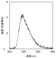
- (A)-(c) is a circuit diagram which shows the power supply circuit in which the drive power supply contained in the light-emitting device of one Embodiment of this invention applies a voltage to a light emitting element, respectively. It is a manufacture flowchart of the light emitting element produced by EL experiment. It is the emission spectrum of the light emitting element produced by EL experiment.
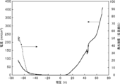
- FIG. 6 is a graph showing IV characteristics and light emission-voltage characteristics of a light emitting device manufactured in an EL experiment. It is the graph which showed the light emission time characteristic of the light emitting element produced by EL experiment. It is the graph which showed the relationship between the heat processing temperature of the light emitting element produced in EL experiment, and emitted light intensity. It is the graph which showed the relationship between the germanium density
- the light emitting device of the present invention includes a semiconductor layer, a first electrode, a dielectric layer sandwiched between the semiconductor layer and the first electrode, a light emitting element including a light emitter, the semiconductor layer and the first electrode, A light source circuit for applying a voltage between the semiconductor layer, the dielectric layer, the semiconductor layer and the dielectric layer, and the first electrode.
- the light emitting device is formed in at least one region between the dielectric layer and the light emitting element when a current is passed through the dielectric layer with the semiconductor layer as a positive electrode and a first electrode as a negative electrode.
- the power supply circuit emits light from the light emitting element, and a current having a constant direction is generated. Serial respectively the semiconductor layer and the first electrode to flow a dielectric layer, characterized in that electrical connection.
- the light emitting element is higher when a current accompanied by light emission of the light emitting element flows through the dielectric layer than when a current without light emission of the light emitting element flows through the dielectric layer. It preferably has electrical resistance. According to such a configuration, the light emitting element can emit light with less power consumption.
- the power supply circuit includes a rectifier diode for flowing a current through the dielectric layer between the semiconductor layer and the first electrode, and the power supply circuit is supplied with power from an AC power supply. It is preferable. According to such a configuration, even when an AC power supply is used as the drive power supply, a voltage can be applied to the light emitting element so that a current having a constant direction flows through the dielectric layer.
- the power supply circuit is supplied with power from a DC power supply. According to such a configuration, a voltage can be applied to the light emitting element such that a current having a constant direction flows through the dielectric layer.
- the semiconductor layer is made of an n-type semiconductor or a p-type semiconductor, and the power supply circuit is configured such that when the semiconductor layer is made of an n-type semiconductor, the semiconductor layer is a positive electrode and the first electrode is a negative electrode.
- the semiconductor layer and the first electrode are electrically connected to each other, and the semiconductor layer is made of a p-type semiconductor, the semiconductor layer and the first electrode are arranged so that the semiconductor layer becomes a negative electrode and the first electrode becomes a positive electrode. It is preferable to be electrically connected to the electrodes.
- the light emitting element can emit light by applying a voltage to the light emitting element such that a current having a constant direction flows through the dielectric layer.
- the light emitter includes a germanium atom. According to such a configuration, the light emitting element can emit light. In the light emitting device of the present invention, the light emitter preferably contains ZnS. According to such a configuration, the light emitting element can emit light. In the light emitting device of the present invention, it is preferable that the light emitting element has a surface temperature of 60 ° C. or lower when a current accompanied by light emission flows through the dielectric layer. According to such a configuration, even if the light emitting element is mounted on the photoelectric hybrid circuit, it is possible to suppress the influence on the other elements due to heat generation of the light emitting element. In addition, even when the light-emitting element is used as a light source such as an illumination, the influence on luminance deterioration due to heat generation of the light-emitting element can be suppressed.
- FIG. 1 is an explanatory diagram showing the configuration of a light emitting device according to an embodiment of the present invention.
- the light-emitting element 12 is shown in a schematic cross-sectional view, and the drive power supply 15 and the power supply circuit for applying a voltage to the light-emitting element 12 are shown in a circuit diagram and the like.
- the light emitting device 20 of the present embodiment includes a light emitting element 12 including a semiconductor layer 1, a first electrode 7, a dielectric layer 3 sandwiched between the semiconductor layer 1 and the first electrode 7, and a light emitter 5.
- a power supply circuit 13 for applying a voltage between the semiconductor layer 1 and the first electrode 7 is provided.
- the light emitter 5 includes the semiconductor layer 1, the dielectric layer 3, and the semiconductor layer 1 and the dielectric layer. 3 and between the first electrode 7 and the dielectric layer 3, the light emitting element 12 includes the dielectric layer 3 with the semiconductor layer 1 as a positive electrode and the first electrode 7 as a negative electrode.
- the light emitting element 12 includes a semiconductor layer 1, a first electrode 7, a dielectric layer 3 sandwiched between the semiconductor layer 1 and the first electrode 7, and a light emitter 5.
- the light emitter 5 includes at least one region in the semiconductor layer 1, in the dielectric layer 3, between the semiconductor layer 1 and the dielectric layer 3, and between the first electrode 7 and the dielectric layer 3. Is formed.
- the light emitting element 12 has a current flowing through the dielectric layer 3 when the semiconductor layer 1 is used as the positive electrode and the first electrode 7 as the negative electrode, and when the current flows through the dielectric layer 3 using the semiconductor layer 1 as the negative electrode and the first electrode 7 as the positive electrode.
- the current flowing through the dielectric layer 3 when the light emitting element 12 emits light is referred to as “current accompanied by light emission”, and the current flowing through the dielectric layer 3 when the light emitting element 12 does not substantially emit light is expressed as “ It is called “current without emission”.
- the light emitting element 12 may be an inorganic EL element. Further, “the light emitting element 12 does not substantially emit light” means that the light emitting element 12 does not emit light even when a current flows through the dielectric layer 3, and that “a current without light emission” flows through the dielectric layer 3. The amount of light emitted at that time is sufficiently smaller than the amount of light emitted when “current with light emission” flows.
- the light emitting element 12 may have a higher electrical resistance when a current accompanied by light emission flows through the dielectric layer 3 than when a current without light emission flows through the dielectric layer 3.
- the magnitude of the “current without emission” is the magnitude of the “current with emission”. It will be bigger than that.
- the light emission voltage threshold is ⁇ V a and the current value at this time is ⁇ I 1
- the current value + I 2 at the time of applying the voltage + V a is
- the light emitting mechanism of the light emitting element 12 is such that an electric field is formed in the dielectric layer 3 and the semiconductor layer 1 by a voltage applied between the semiconductor layer 1 and the first electrode 7, and the dielectric layer 3 or the first electrode 7 It is considered that the electrons introduced into the layer 3 are accelerated by this electric field, and the accelerated electrons excite the light emitter 5 and its excitation level is relaxed, so that the light emitter 5 emits light.
- the semiconductor layer 1 is provided so as to sandwich the dielectric layer 3 between the first electrode 7 and can serve as an electrode for applying a voltage to the dielectric layer 3 by the driving power supply 15.
- the semiconductor layer 1 consists of a semiconductor which can become an electrode,
- it can be set as a p-type semiconductor or an n-type semiconductor.
- the resistivity can be adjusted by impurity doping.
- it is considered that there is a merit in terms of occupied area or the like when it is manufactured as a semiconductor substrate rather than being configured as a discrete element and bonded.
- the semiconductor layer 1 may have both a p-type semiconductor and an n-type semiconductor on the surface in contact with the dielectric layer 3.
- the semiconductor layer 1 may be a semiconductor layer formed on a substrate, a semiconductor substrate, or a part of the semiconductor substrate. More specifically, for example, a p-type silicon substrate or an n-type silicon substrate can be used. Alternatively, p-type silicon or n-type silicon may be formed on a SiO 2 substrate or the like. A dielectric layer 3 such as SiO 2 is formed on a Si substrate, and p-type silicon or n-type silicon is formed thereon. May be formed.
- the light emitting element 12 may be formed on a crystalline silicon substrate included in an SOI (Silicon On Insulator) substrate, or amorphous silicon or the like may be formed on the dielectric layer 3 such as SiO 2 by using a CVD method or the like.
- the light emitting element 12 may be formed thereon.
- the first electrode 7 is provided so as to sandwich the dielectric layer 3 between the semiconductor layer 1 and can serve as an electrode for applying a voltage to the dielectric layer 3 by a driving power source. Although it will not specifically limit if the 1st electrode 7 becomes an electrode, It is preferable to have translucency.
- the first electrode 7 can be, for example, a translucent electrode. Further, the first electrode 7 may have a light transmittance of 60% or more and 99.99% or less with a wavelength of 300 nm or more and 500 nm or less. Thereby, the light emission of the light emitter 5 can be taken out from the first electrode side.
- the first electrode 7 is, for example, a metal oxide thin film such as ITO, a metal thin film such as Al, Ti, or Ta, or a semiconductor thin film such as Si, SiC, or GaN.
- the dielectric layer 3 is provided so as to be sandwiched between the semiconductor layer 1 and the first electrode 7.
- the dielectric layer 3 is made of silicon oxide, silicon nitride, or silicon oxynitride. Further, since silicon oxide, silicon nitride, or silicon oxynitride can be formed by a normal silicon semiconductor process, it is excellent in mass productivity and can be combined with other electronic circuits. Further, when the dielectric layer 3 is made of silicon oxide and the semiconductor layer 1 is made of a silicon substrate, the dielectric layer 3 can be made a thermal oxide film of the silicon substrate and can be easily formed.
- the thickness of the dielectric layer 3 can be, for example, 10 nm to 100 nm (for example, a range between any two of 10, 20, 30, 40, 50, 60, 70, 80, 90, and 100 nm). .
- the dielectric layer 3 can have translucency. Thereby, the light emission of the light emitter 5 can be taken out.
- the light transmittance of the dielectric layer 3 is preferably 80% or more, for example, for light with a wavelength of 300 to 500 nm.
- the peak wavelength of the light emitted from the light emitter 5 is around 390 nm. Therefore, if the light transmittance at a wavelength of 300 to 500 nm is high, the light extraction efficiency is correspondingly increased. Because it becomes higher.
- the light emitter 5 is disposed in at least one region of the semiconductor layer 1, the dielectric layer 3, between the semiconductor layer 1 and the dielectric layer 3, and between the first electrode 7 and the dielectric layer 3. It is formed.
- FIG. 2 is a cross-sectional view of the light emitting device 12 of various embodiments.
- the light emitter 5 may be formed in the dielectric layer 3 as shown in FIG. 1, or may be formed in the semiconductor layer 1 as shown in FIG. Further, the light emitter 5 may exist as an atom or a fine particle in the semiconductor layer 1 or the dielectric layer 3. Further, the light emitter 5 may be formed in layers as shown in FIGS. 2 (b) to 2 (d).
- the layered light emitter 5 may be formed so as to be sandwiched between the dielectric layers 3 as shown in FIG. 2B, and between the semiconductor layer 1 and the dielectric layer 3 as shown in FIG. It may be formed, or may be formed between the dielectric layer 3 and the first electrode 7 as shown in FIG.
- Examples of the atomic light emitter 5 include a germanium atom, a silicon atom, or a tin atom, and can be formed by ion-implanting a germanium atom or the like into the dielectric layer 3 made of silicon oxide.
- Examples of the fine-particle light emitter 5 include germanium fine particles.
- Examples of the layered light emitter 5 include a layer made of ZnS.
- the germanium fine particles can be formed by, for example, ion-implanting germanium atoms into the dielectric layer 3 made of silicon oxide and aggregating the germanium atoms by performing a heat treatment. In this case, the formed germanium fine particles can be heat-treated to form germanium fine particles containing germanium oxide. Further, the germanium atom contained in the germanium oxide may be +2 or +4, a +2 germanium atom (hereinafter abbreviated as Ge 2+ ) and a +4 valent germanium atom (hereinafter referred to as “Ge2 +” ). Abbreviated as Ge 4+ ).
- the number density of atoms constituting the light emitter 5 in the dielectric layer 3 is, for example, 1 ⁇ 10 16 atoms / cm 3 to 1 ⁇ 10 21 atoms / cm 3 .
- the phosphor 5 is preferably a fine particle having a maximum particle size of 1 nm or more and 20 nm or less. This is because the luminous efficiency is particularly high in this case.
- the “maximum grain size” is a 100 nm square range of an arbitrary cross section of the dielectric layer 3 (a cross section as shown in FIG. 1 or a cross section perpendicular to the paper surface). Means the particle diameter of the largest particle among the fine particles that can be observed by TEM observation. Further, in the present invention, “particle size” means the length of the longest line segment that can be projected on a TEM photograph and included in a planar image of a fine particle when viewed with a cross-sectional TEM photograph.
- the maximum particle size of the fine particles is, for example, 1, 2, 3, 4, 5, 6, 7, 8, 9, 10, 12, 14, 16, 18, or 20 nm.
- the maximum particle diameter of the fine particles may be within a range between any two numerical values exemplified here, or may be equal to or smaller than any one numerical value.
- the ratio of Ge 2+ to the entire germanium oxide (Ge 4+ + Ge 2+ ) is attributed to the area of the peak S Ge4 + due to Ge 4+ and Ge 2+ in the spectrum near the 3d peak of Ge in the XPS spectrum.
- the peak area S Ge2 + can be obtained and S Ge2 + / (S Ge4 + + S Ge2 + ) can be obtained.
- As an X-ray source for XPS measurement for example, monochromatic Al and K ⁇ rays (1486.6 eV) can be used.
- the peak due to Ge 4+ and the peak due to Ge 2+ are overlapped with each other, but the Gaussian fitting is performed, and the peak due to Ge 4+ is separated from the peak due to Ge 2+ by waveform separation.
- Ge4 + and SGe2 + can be determined.
- the peak energies of Ge 4+ and Ge 2+ are about 33.5 eV and 32 eV, respectively.
- the Ge 2+ may contain 10% or more when the total of Ge 2+ and Ge 4+ contained in the luminescent body 5 to 100% . If the ratio of Ge 2+ is too small, there is a possibility that light is not emitted or the emission intensity is too small. Specifically, the proportion of Ge 2+ is, for example, 10, 20, 30, 40, 50, 60, 70, 80, 90, 95, 99, 100%. The ratio of Ge 2+ may be within a range between any two of the numerical values exemplified here.
- the peak area S Ge caused by zero-valent germanium (hereinafter abbreviated as Ge 0 ) and the peak caused by germanium oxide (Ge 2+ + Ge 4+ ).
- the area S of Ge oxide is obtained, and S Ge2 + / (S Ge + S Ge oxide) is calculated to obtain the Ge oxidation rate.
- the average value of this oxidation rate is not specifically limited, For example, 1, 5, 10, 15, 20, 25, 30, 34.9, 35, 40, 45, 50, 55, 60, 60.1, 65 , 70, 70.1, 75, 80, 85, 90, 95, 99, 100%.
- the average value of the oxidation rate may be within a range between any two of the numerical values exemplified here.
- the light emitting element 12 has a peak of electroluminescence (EL) wavelength when a voltage is applied between the semiconductor layer 1 and the first electrode 7. Is in the range of 340 to 440 nm (more strictly speaking, 350 to 430 nm, 360 to 420 nm, 370 to 410 nm, 380 to 400 nm, or 385 to 395 nm).
- EL electroluminescence
- the second electrode 10 is formed so as to be electrically connected to the semiconductor layer 1.
- the semiconductor layer 1 can be connected to the drive power supply 15 through the second electrode.
- the semiconductor layer 1 can be grounded via the second electrode.
- the second electrode 10 can be a metal electrode such as an aluminum electrode, for example.
- the drive power supply 15 applies a voltage between the semiconductor layer 1 and the first electrode 7 so that a current having a constant direction flows through the dielectric layer 3 with light emission of the light emitting element 12.
- the power output from the drive power supply 15 is supplied to the light emitting element 12 by the power supply circuit 13.
- the drive power supply 15 may be a DC power supply or an AC power supply as long as the direction of the current flowing through the dielectric layer 3 is constant.
- the drive power supply 15 may include a rectifier diode 16 in the power supply circuit 13 for applying a voltage to the dielectric layer 3. This makes it possible to convert the power supply having the opposite polarity and output a desired polarity voltage.
- the drive power supply 15 may include a step-up circuit or a step-down circuit in the power supply circuit 13 for applying a voltage to the dielectric layer 3.
- the output of the drive power supply 15 can be converted into a desired voltage value and output to the light emitting element 12.
- the “current having a constant direction” means a current having a constant direction in which the current value increases as the applied voltage increases.
- the drive power supply 15 When the drive power supply 15 is an AC power supply, the drive power supply may be a power supply that outputs a voltage having a desired waveform.
- the drive power supply 15 may output, for example, a rectangular wave voltage or a sine wave voltage.
- FIGS. 3A to 3C are circuit diagrams showing various power supply circuits 13 for outputting a voltage to the light emitting element 12 by the drive power supply 15.
- the drive power supply 15 is a low voltage sine wave AC power supply as shown in FIG. 3A, and a booster circuit and a rectifier diode 16 are provided between the light emitting element 12 and electrically connected to the light emitting element 12. Good.
- the voltage output from the drive power supply 15 can be converted into a desired voltage value by the booster circuit, and only a half wave can be output to the light emitting element 12 by the rectifier diode 16. Accordingly, a current having a constant direction of current flow can be supplied to the light emitting element 12. By making the direction of this current the same as the direction in which the current flows with the light emission of the light emitting element, the light emitting element can emit light.
- the drive power supply 15 may be an AC power supply as shown in FIG. 3B, for example, and may be electrically connected to the light emitting element 12 by providing a step-down circuit and a rectifier diode 16 between the light emitting element 12.
- the voltage output from the drive power supply 15 can be converted into a desired voltage value by the booster circuit, and only a half wave can be output to the light emitting element 12 by the rectifier diode 16.
- the drive power supply 15 may be a direct current power supply as shown in FIG. 3C, for example, and may be electrically connected to the light emitting element 12 by providing a DCDC conversion circuit with the light emitting element 12. With the DCDC conversion circuit, the voltage output from the drive power supply 15 can be converted into a desired voltage value and output to the light emitting element 12.
- a method for manufacturing the light-emitting element 12 when the light emitter 5 is made of germanium fine particles will be described below. 1. Formation of Semiconductor Layer When the p-type silicon substrate or the n-type silicon substrate is used as the semiconductor layer 1, these can be used as the semiconductor layer 1. Further, the semiconductor layer 1 may be formed on a part of the silicon substrate by diffusing p-type impurities or n-type impurities in the silicon substrate.
- dielectric layer 3 is formed on the semiconductor layer 1.
- the dielectric layer 3 made of silicon oxide can be formed by heat-treating a silicon substrate, and the dielectric layer 3 can also be formed by depositing silicon oxide or silicon nitride by CVD or sputtering.
- a light emitter 5 is formed inside the dielectric layer 3.
- a method for forming the light emitter 5 inside the dielectric layer 3 is not particularly limited, but a method is conceivable in which germanium is ion-implanted into the dielectric layer 3 and then heat treatment is performed. By the heat treatment after ion implantation, germanium ions are aggregated to form a large number of fine particles in the dielectric layer 3 and Ge 0 is oxidized to form germanium oxide containing Ge 2+ and Ge 4+ .
- the ion implantation of germanium can be performed, for example, under conditions of an implantation energy of 5 to 100 keV and an implantation amount of 1 ⁇ 10 14 to 1 ⁇ 10 17 ions / cm 2 .
- the ratio of Ge 2+ to Ge 4+ can be appropriately adjusted by changing the amount of germanium implanted, the heat treatment time, the heat treatment temperature, the heat treatment atmosphere, and the like. Specifically, the Ge 2+ ratio can be increased by adjusting the partial pressure and flow rate of oxygen in the heat treatment atmosphere. For example, when the atomic concentration of germanium in silicon oxide having a film thickness of 100 nm is 10% or less, in the heat treatment at 800 ° C. for 1 hour, an inert gas is supplied while evacuating (400 liters per minute) (50 minutes per minute). In the case of milliliters), germanium partially binds to oxygen but oxygen is insufficient, so that it is not completely oxidized and Ge 2+ can be generated.
- Ge 4+ In an atmosphere of 1 atm in which oxygen with a volume of 20% is mixed with an inert gas, a large amount of Ge 4+ is formed due to excessive supply of oxygen, and Ge 2+ decreases.
- the atmosphere suitable for increasing the Ge 2+ ratio depends on other parameters such as germanium implantation conditions, heat treatment time, and temperature, but in one example, the germanium atomic concentration is relatively high, and the inert gas The ratio of Ge 2+ can be increased by supplying gas mixed with oxygen while evacuating .
- germanium is preferably ion-implanted so that the germanium concentration in the dielectric layer 3 is 0.1 to 10.0 atomic%. This is because when the inert gas is supplied (50 milliliters per minute) while evacuating (400 liters per minute) in a heat treatment at 600 ° C. for 1 hour, the luminous efficiency is relatively high in this range.
- the germanium concentration is, for example, 0.1, 0.2, 0.3, 0.4, 0.5, 0.6, 0.7, 0.8, 0.9, 1.0, 2 0.0, 3.0, 4.0, 5.0, 6.0, 7.0, 8.0, 9.0, 10.0 atomic%. This concentration may be within a range between any two of the numerical values exemplified herein.
- the germanium concentration can be measured, for example, by a high resolution RBS (Rutherford backscattering) method. In addition, it can be measured by various analysis methods such as SIMS (secondary ion mass spectrometry).
- the germanium concentration is measured in a range where the germanium concentration is 1/100 or more of the peak value.
- the temperature of the heat treatment is preferably 400 to 900 ° C, more preferably 500 to 800 ° C. This is because the luminous efficiency is relatively high in this range.
- a translucent electrode as the first electrode 7 is formed on the dielectric layer 3 on which the light emitter 5 is formed.
- an ITO electrode can be formed by a coating method, sputtering, or the like.
- the second electrode 10 is formed so as to be electrically connected to the semiconductor layer 1.
- the formation method is not particularly limited, the aluminum electrode can be formed on the semiconductor layer 1 by, for example, a coating method, sputtering, or the like.
- FIG. 4 is a flowchart of a manufacturing method of the light emitting element 12.
- an n-type silicon substrate having an impurity concentration of 5 ⁇ 10 15 cm ⁇ 3 was thermally oxidized at 1050 ° C. in an oxygen atmosphere to form a 60 nm silicon thermal oxide film on the surface.
- Ge ions were implanted into the silicon thermal oxide film at 50 keV under the condition of 9.2 ⁇ 10 15 ions / cm 2 .
- the silicon substrate on which the thermal oxide film was formed was placed in an electric furnace, and nitrogen was introduced while being drawn with a rotary pump, followed by heat treatment at 600 ° C. for 1 hour.
- an ITO electrode was formed on the silicon thermal oxide film, an aluminum electrode was formed on the silicon substrate side, and a light emitting element used for EL experiments was obtained.
- the manufactured EL element has a cross section like the cross sectional view of the light emitting element 12 shown in FIG.
- the aluminum electrode of this light emitting element is connected to the ground, and the ITO electrode is set to about ⁇ 40 V, so that the silicon thermal oxide film has the n-type silicon substrate (semiconductor layer 1) as the positive electrode and the ITO electrode (first electrode 7) as the negative electrode. (Dielectric layer 3) When voltage was applied, blue light emission was confirmed.
- the silicon thermal oxide film has the n-type silicon substrate (semiconductor layer 1) as the positive electrode and the ITO electrode (first electrode 7) as the negative electrode. (Dielectric layer 3)
- the silicon thermal oxide film has the n-type silicon substrate (semiconductor layer 1) as the positive electrode and the ITO electrode (first electrode 7) as the negative electrode. (Dielectric layer 3)
- the silicon thermal oxide film has the n-type silicon substrate (semiconductor layer 1) as the positive electrode and the ITO electrode (first electrode 7) as the negative electrode. (Dielectric layer 3)
- blue light emission was confirmed.
- FIG. 5 shows an emission spectrum of blue light emission of the manufactured EL element.
- the confirmed blue emission was light having a wavelength of 340 nm to 550 nm, and electroluminescence emission having a peak between 340 nm and 440 nm.
- a light emitting element is manufactured in the same manner using an n-type silicon substrate or a p-type silicon substrate having an impurity concentration of 1.0 ⁇ 10 17 cm ⁇ 3 , and a voltage is applied to the ITO electrode with respect to the silicon substrate. Although applied, no luminescence was confirmed.
- a light-emitting element was manufactured by a similar method using a p-type silicon substrate having an impurity concentration of 5 ⁇ 10 15 cm ⁇ 3 , and light emission was confirmed when a voltage was applied to the ITO electrode with respect to the silicon substrate.
- a light-emitting element can be made to emit electroluminescence by manufacturing a light-emitting element using a silicon substrate having an impurity concentration of 5 ⁇ 10 15 cm ⁇ 3 or less.
- the aluminum electrode of the manufactured EL element was connected to the ground, and the ITO electrode was changed to have a potential of ⁇ 70 V to +70 V, and the IV characteristic and the light emission-voltage characteristic of the EL element were measured.
- the measurement results are shown in FIG. Referring to FIG. 6, when a voltage is applied so that the ITO electrode has a negative potential, the EL element emits light when a current flows through the EL element, and a voltage is applied so that the ITO electrode has a positive potential. In this case, it can be seen that the EL element hardly emits light even when a current flows through the EL element.
- the electric resistance value of the EL element is higher than that when a current without current flows (when the ITO electrode is set to a positive potential, that is, when a voltage is applied to the thermal oxide film using the silicon substrate as a negative electrode and the ITO electrode as a positive electrode). It can be seen that the power consumption is large and the power consumption is small.
- the light emission voltage threshold value ⁇ V a of the EL element was ⁇ 40 V, and the current value ⁇ I 1 at this time was ⁇ 4.3 mA / cm 2 .
- the current value + I 2 was +126 mA / cm 2 when a voltage + V a 40 V having the opposite sign of the light emission threshold was applied to the EL element. This satisfies the condition of “
- thermocouple wrapped with a thin polyimide tape is attached to the surface of an aluminum electrode connected to the ground of the produced EL element, and a driving power source is connected to the ITO electrode in an atmosphere at 25 ° C.
- a voltage was applied to the EL element by the application methods 1 to 8, and the surface temperature of the EL element was measured.
- the reason why the thermocouple is wrapped with the polyimide tape is to prevent the current flowing through the EL element from applying a voltage to affect the temperature measurement.
- the measurement results are shown in Table 1.
- the device temperatures shown in Table 1 were calculated by calculating the average value measured for 100 seconds after applying the voltage by each method and the device temperature reached the saturation state.
- Voltage application methods 1 to 3 in Table 1 show the element surface temperature when a rectangular wave voltage is applied to the EL element, and the maximum voltage and the minimum voltage are respectively changed.
- the element surface temperature was 70 ° C. or higher, whereas in the voltage application method 3, the element surface temperature was suppressed to about 30 ° C.
- the maximum voltage is +60 V
- the ITO electrode serves as the positive electrode and the silicon substrate serves as the negative electrode, and a current (current without light emission) flows through the thermal oxide film. Is 0 V, it is considered that “current without light emission” does not flow. Therefore, it was found that the EL element generates a large amount of heat when “current without emission” flows. It was also found that heat generation of the EL element can be suppressed by applying a voltage to the EL element so that this “current without light emission” does not flow.
- the ITO electrode serves as a negative electrode and the silicon substrate serves as a positive electrode, and a current (current accompanied by light emission) flows through the thermal oxide film. Since the voltage is 0 V, it is considered that “current with light emission” does not flow.
- the element surface temperature is suppressed to about 30 ° C., and the voltage application method 1 is only about 15 ° C. higher than the voltage application method 2. Accordingly, it was found that the amount of heat generated by the EL element is small even when “current with light emission” flows.
- the voltage application method 4 in Table 1 shows the element surface temperature when a sine wave voltage of the maximum voltage +60 V and the minimum voltage -60 V is applied to the EL element. Compared with the voltage application method 1 in which the maximum voltage and the minimum voltage are the same, the voltage application method 4 suppresses the temperature rise. This is considered to be because the “current without light emission” is smaller because the applied voltage of the voltage applying method 4 is a sine wave.
- the voltage application methods 5 and 6 in Table 1 show the element surface temperature when a direct current voltage is applied to the EL element so that the ITO electrode becomes ⁇ 60V or + 60V.
- the element surface temperature is kept as low as 35 ° C. This is presumably because “current with light emission” flows but “current without light emission” does not flow because a voltage is applied so that the ITO electrode becomes ⁇ 60V.
- the element temperature is as high as 115 ° C. This is presumably because a large amount of “current with light emission” flows and no “current without light emission” flows because a voltage is applied so that the ITO electrode becomes + 60V.
- the duty ratio is (positive voltage application time) / (positive voltage application time + negative voltage application time). From these results, it was found that the device surface temperature increased as the positive voltage application time was increased.
- the LSI and the light-emitting elements are densely packed, and the LSI is strongly influenced by temperature, so that heat generation is preferably small.
- the element surface temperature be suppressed to 85 ° C. or lower. This is because 85 ° C. is one of the reliability standards for LSI and the like.
- the element surface temperature is preferably suppressed to 60 ° C. or lower.
- the drive power supply applies only a voltage having polarity to the light emitting element.
- the driving power source may be configured by a DC power source or an AC power source having a diode in the subsequent stage.
- the light emission time when applied was measured. The result is shown in FIG. As can be seen from FIG. 7, when the voltage is applied to the EL element by the voltage application method 3, the emission intensity is less deteriorated than when the voltage is applied to the EL element by the voltage application method 1.
- the EL element to which a voltage is applied by the voltage applying method 3 is about 20 times longer than the EL element to which a voltage is applied by the voltage applying method 1.
- the EL element produced in this experiment contained germanium atoms or germanium oxide as the light emitter, the EL element may contain ZnS as the light emitter. In addition, the EL element may contain germanium atoms or both germanium oxide and ZnS.
- An EL element can be manufactured by further introducing ZnS into a light-emitting layer containing germanium atoms or germanium oxide using an ion implantation method or a CVD method.
- germanium oxide including Ge 4+ and Ge 2+
- germanium oxide was involved in light emission of the light-emitting element included in the present invention by the following method.
- the first hypothesis is that the Ge nanoparticles emit light due to the quantum size effect. This light emission mechanism is the same as the light emission mechanism of normal nanoparticles, and the emission wavelength depends on the particle size.
- germanium oxide including Ge 4+ and Ge 2+ ) is involved in light emission. Since the energy level difference between the excited state and the ground state of GeO (Ge 2+ ) is 2.9 to 3.2 eV (387 to 427 nm) (L. Skuja, J. Non-Cryst. Solids, 239 (1998). ) 16-48)), according to the second hypothesis, the emission wavelength is about 387 to 427 nm, which is considered to be independent of the particle size.
- a light emitting device was manufactured under various temperature conditions and injection conditions different from each other, and the EL wavelength when a voltage was applied to the device by the above method was measured.
- the EL wavelength “Spectrofluorimeter RF-5300PC manufactured by Shimadzu Corporation” was used.
- the manufacturing method of the light emitting element is as described in “1. Effect confirmation experiment” except that the heat treatment temperature and the Ge implantation amount are appropriately changed.
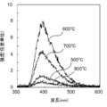
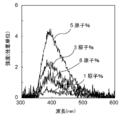
- the obtained results are shown in FIGS.
- the temperature in FIG. 8 shows the heat treatment temperature (time is 1 hour) after Ge implantation.
- “Atom%” in FIG. 9 indicates the Ge concentration in the silicon oxide film after Ge implantation.
- the Ge concentration in FIG. 8 is 5.0 atomic%, and the heat treatment temperature after Ge implantation in FIG. 9 is 700 ° C. (time is 1 hour).
- the peak wavelength of the EL is substantially constant at 390 nm even if the heat treatment temperature and the Ge concentration are changed.
- the size of the formed nanoparticles also changes, so that the EL peak wavelength should be shifted if the light emission mechanism follows the first hypothesis. Therefore, the EL wavelength confirmed in FIGS. 8 and 9 cannot be explained by the first hypothesis.
- the wavelength of 390 nm is within the range of the emission wavelength (387 to 427 nm) predicted by the second hypothesis.
- the EL wavelength from the light-emitting element of the present invention cannot be explained by the first hypothesis but can be explained by the second hypothesis. Therefore, it was confirmed that germanium oxide (including Ge 4+ and Ge 2+ ) was involved in light emission of the light-emitting element of the present invention.
- the heat treatment temperature is preferably 600 to 700.degree.
- the Ge concentration is preferably 3.0 atomic% or more, and more preferably 3.0 to 5.0 atomic%.
- a light emitting device was fabricated according to the method described in “1. Effect Confirmation Experiment”, and Ge 0 , Ge 2+ , Ge 4 in the silicon oxide film The depth distribution of the percentage of + was investigated.
- the light-emitting element manufactured here has a Ge concentration of 5.0 atomic% and a heat treatment temperature of 800 ° C. (time is 1 hour). Since XPS can usually analyze in the range of several nanometers deep from the sample surface, Ge 0 , Ge 2+ , Ge 4+ in a region up to a depth of 50 nm can be obtained by alternately performing etching with an argon ion beam and XPS measurement.
- FIG. 10 shows the XPS measurement results at that time in which the graphs are translated and arranged in the vertical direction for easy understanding.
- FIG. 11 is a graph showing the state of Ge atoms included in each depth by the ratio of Ge 0 , Ge 2+ and Ge 4+ .
- the ratio of non-oxidized Ge 0 is 30 to 70%.
- Ge 4+ is between 0-20 % and approximately 10%.
- Ge 2+ in which Ge is not completely oxidized but partially oxidized is between 10% and 50%.
- the ratio of Ge 0 , Ge 2+ , and Ge 4+ at each depth indicates the peak area S Ge caused by Ge 0 and the peak caused by Ge 2+ in the XPS spectrum near the 3d peak of Ge in the spectrum.
- the XPS spectrum was measured using monochromatic Al and K ⁇ rays (1486.6 eV) as an X-ray source.
Landscapes
- Physics & Mathematics (AREA)
- Engineering & Computer Science (AREA)
- Microelectronics & Electronic Packaging (AREA)
- Optics & Photonics (AREA)
- Electroluminescent Light Sources (AREA)
Abstract
本発明の発光装置は、半導体層と、第1電極と、前記半導体層と第1電極とに挟まれた誘電体層と、発光体とを含む発光素子と、前記半導体層と第1電極との間に電圧を印加するための電源回路とを備え、前記発光体は、前記半導体層の中、前記誘電体層の中、前記半導体層と前記誘電体層との間、および第1電極と前記誘電体層との間のうち少なくとも1つの領域に形成され、前記発光素子は、前記半導体層を正極とし第1電極を負極として前記誘電体層に電流を流した場合および前記半導体層を負極とし第1電極を正極として前記誘電体層に電流を流した場合のうち、一方の場合では電流を流すと発光するのに対し、他方の場合では電流を流しても実質的に発光せず、前記電源回路は、前記発光素子の発光を伴い、向きが一定の電流が前記誘電体層を流れるように前記半導体層および第1電極とそれぞれ電気的に接続することを特徴とする。
Description
本発明は、発光装置に関する。
無機エレクトロルミネセンス(EL)素子は長寿命であって、省電力であるところから表示装置や次世代の面発光表示装置として注目されている。無機EL素子を発光させるためには、200~300 V の電圧を無機EL素子に印加する必要がある。従来の無機EL素子に電圧を印加する電源装置は、商用交流を昇圧し無機EL素子に印加する基本構成となっており、定電圧および定周波数の交流を出力して無機EL素子を発光させる(たとえば、特許文献1)。より具体的には、電流共振型の直列共振回路による昇圧回路により、無機EL素子に正弦波電圧を印加する方法が挙げられる。
しかし、従来の電源装置により無機EL素子に電圧を印加し無機EL素子を発光させると、無機EL素子が発熱するという問題があった。
本発明は、このような事情に鑑みてなされたものであり、電圧の印加に伴う発熱が抑制された発光装置を提供する。
本発明は、このような事情に鑑みてなされたものであり、電圧の印加に伴う発熱が抑制された発光装置を提供する。
本発明は、半導体層と、第1電極と、前記半導体層と第1電極とに挟まれた誘電体層と、発光体とを含む発光素子と、前記半導体層と第1電極との間に電圧を印加するための電源回路とを備え、前記発光体は、前記半導体層の中、前記誘電体層の中、前記半導体層と前記誘電体層との間、および第1電極と前記誘電体層との間のうち少なくとも1つの領域に形成され、前記発光素子は、前記半導体層を正極とし第1電極を負極として前記誘電体層に電流を流した場合および前記半導体層を負極とし第1電極を正極として前記誘電体層に電流を流した場合のうち、一方の場合では電流を流すと発光するのに対し、他方の場合では電流を流しても実質的に発光せず、前記電源回路は、前記発光素子の発光を伴い、向きが一定の電流が前記誘電体層を流れるように前記半導体層および第1電極とそれぞれ電気的に接続することを特徴とする発光装置を提供する。
本発明によれば、発光素子は、半導体層と、第1電極と、前記半導体層と第1電極とに挟まれた誘電体層と、発光体とを含み、前記発光体は、前記半導体層の中、前記誘電体層の中、前記半導体層と前記誘電体層との間、および第1電極と前記誘電体層との間のうち少なくとも1つの領域に形成されるため、半導体層と第1電極との間に電圧を印加することにより、発光素子を発光させることができる。
本発明によれば、発光素子は、半導体層を正極とし第1電極を負極として誘電体層に電流を流した場合および半導体層を負極とし第1電極を正極として誘電体層に電流を流した場合のうち、一方の場合では電流を流すと発光するのに対し、他方の場合では電流を流しても実質的に発光しないため、発光素子が発光する向きで一定の電流を誘電体層に流れるように電圧を発光素子に印加することにより、発光素子をより少ない消費電力で効率よく発光させることができる。
本発明によれば、実質的に発光しない方向の電流が誘電体層に流れないように発光素子に電圧を印加するため、駆動電源が印加した電力が熱に変換されることを抑制することができ、発光素子の発熱を抑制することができる。
本発明によれば、発光素子は、半導体層を正極とし第1電極を負極として誘電体層に電流を流した場合および半導体層を負極とし第1電極を正極として誘電体層に電流を流した場合のうち、一方の場合では電流を流すと発光するのに対し、他方の場合では電流を流しても実質的に発光しないため、発光素子が発光する向きで一定の電流を誘電体層に流れるように電圧を発光素子に印加することにより、発光素子をより少ない消費電力で効率よく発光させることができる。
本発明によれば、実質的に発光しない方向の電流が誘電体層に流れないように発光素子に電圧を印加するため、駆動電源が印加した電力が熱に変換されることを抑制することができ、発光素子の発熱を抑制することができる。
本発明の発光装置は、半導体層と、第1電極と、前記半導体層と第1電極とに挟まれた誘電体層と、発光体とを含む発光素子と、前記半導体層と第1電極との間に電圧を印加するための電源回路とを備え、前記発光体は、前記半導体層の中、前記誘電体層の中、前記半導体層と前記誘電体層との間、および第1電極と前記誘電体層との間のうち少なくとも1つの領域に形成され、前記発光素子は、前記半導体層を正極とし第1電極を負極として前記誘電体層に電流を流した場合および前記半導体層を負極とし第1電極を正極として前記誘電体層に電流を流した場合のうち、一方の場合では電流を流すと発光するのに対し、他方の場合では電流を流しても実質的に発光せず、前記電源回路は、前記発光素子の発光を伴い、向きが一定の電流が前記誘電体層を流れるように前記半導体層および第1電極とそれぞれ電気的に接続することを特徴とする。
本発明の発光装置において、前記発光素子は、前記誘電体層に前記発光素子の発光を伴う電流が流れる場合、前記誘電体層に前記発光素子の発光を伴わない電流が流れる場合に比べより高い電気抵抗を有することが好ましい。
このような構成によれば、発光素子をより少ない消費電力で発光させることができる。
本発明の発光装置において、前記電源回路は、前記半導体層と第1電極との間の前記誘電体層に電流を流すため整流ダイオードを備え、前記電源回路は、交流電源から電力を供給されることが好ましい。
このような構成によれば、駆動電源に交流電源を用いた場合でも向きが一定の電流が誘電体層に流れるように発光素子に電圧を印加することができる。
このような構成によれば、発光素子をより少ない消費電力で発光させることができる。
本発明の発光装置において、前記電源回路は、前記半導体層と第1電極との間の前記誘電体層に電流を流すため整流ダイオードを備え、前記電源回路は、交流電源から電力を供給されることが好ましい。
このような構成によれば、駆動電源に交流電源を用いた場合でも向きが一定の電流が誘電体層に流れるように発光素子に電圧を印加することができる。
本発明の発光装置において、前記電源回路は、直流電源から電力を供給されることが好ましい。
このような構成によれば、向きが一定の電流が誘電体層に流れるように発光素子に電圧を印加することができる。
本発明の発光装置において、前記半導体層は、n型半導体またはp型半導体からなり、前記電源回路は、前記半導体層がn型半導体からなる場合、前記半導体層が正極となり第1電極が負極となるように前記半導体層および第1電極とそれぞれ電気的に接続し、前記半導体層がp型半導体からなる場合、前記半導体層が負極となり第1電極が正極となるように前記半導体層および第1電極とそれぞれと電気的に接続することが好ましい。
このような構成によれば、向きが一定の電流が誘電体層に流れるように発光素子に電圧を印加することにより発光素子を発光させることができる。
このような構成によれば、向きが一定の電流が誘電体層に流れるように発光素子に電圧を印加することができる。
本発明の発光装置において、前記半導体層は、n型半導体またはp型半導体からなり、前記電源回路は、前記半導体層がn型半導体からなる場合、前記半導体層が正極となり第1電極が負極となるように前記半導体層および第1電極とそれぞれ電気的に接続し、前記半導体層がp型半導体からなる場合、前記半導体層が負極となり第1電極が正極となるように前記半導体層および第1電極とそれぞれと電気的に接続することが好ましい。
このような構成によれば、向きが一定の電流が誘電体層に流れるように発光素子に電圧を印加することにより発光素子を発光させることができる。
本発明の発光装置において、前記発光体は、ゲルマニウム原子を含むことが好ましい。
このような構成によれば、発光素子が発光することができる。
本発明の発光装置において、前記発光体は、ZnSを含むことが好ましい。
このような構成によれば、発光素子が発光することができる。
本発明の発光装置において、前記発光素子は、前記誘電体層に発光を伴う電流が流れた場合60℃以下の表面温度を有することが好ましい。
このような構成によれば、発光素子を光電混載回路に搭載しても発光素子の発熱による他の素子への影響を抑制することができる。また、発光素子を照明等の光源に用いても発光素子の発熱による輝度劣化への影響を抑制することができる。
このような構成によれば、発光素子が発光することができる。
本発明の発光装置において、前記発光体は、ZnSを含むことが好ましい。
このような構成によれば、発光素子が発光することができる。
本発明の発光装置において、前記発光素子は、前記誘電体層に発光を伴う電流が流れた場合60℃以下の表面温度を有することが好ましい。
このような構成によれば、発光素子を光電混載回路に搭載しても発光素子の発熱による他の素子への影響を抑制することができる。また、発光素子を照明等の光源に用いても発光素子の発熱による輝度劣化への影響を抑制することができる。
以下、本発明の一実施形態を図面を用いて説明する。図面や以下の記述中で示す構成は、例示であって、本発明の範囲は、図面や以下の記述中で示すものに限定されない。
発光装置の構成
図1は本発明の一実施形態の発光装置の構成を示す説明図である。図1において、発光素子12は概略断面図で示しており、発光素子12に電圧を印加する駆動電源15および電源回路は回路図などで示している。
図1は本発明の一実施形態の発光装置の構成を示す説明図である。図1において、発光素子12は概略断面図で示しており、発光素子12に電圧を印加する駆動電源15および電源回路は回路図などで示している。
本実施形態の発光装置20は、半導体層1と、第1電極7と、半導体層1と第1電極7とに挟まれた誘電体層3と、発光体5とを含む発光素子12と、半導体層1と第1電極7との間に電圧を印加するための電源回路13とを備え、発光体5は、半導体層1の中、誘電体層3の中、半導体層1と誘電体層3との間、および第1電極7と誘電体層3との間のうち少なくとも1つの領域に形成され、発光素子12は、半導体層1を正極とし第1電極7を負極として誘電体層3に電流を流した場合および半導体層1を負極とし第1電極7を正極として誘電体層3に電流を流した場合のうち、一方の場合では電流を流すと発光するのに対し、他方の場合では電流を流しても実質的に発光せず、電源回路13は、発光素子12の発光を伴い、向きが一定の電流が誘電体層3を流れるように半導体層1および第1電極7とそれぞれ電気的に接続することを特徴とする。
以下、本実施形態の発光装置20について説明する。
以下、本実施形態の発光装置20について説明する。
1.発光素子
発光素子12は、半導体層1と、第1電極7と、半導体層1と第1電極7とに挟まれた誘電体層3と、発光体5とを含む。また、発光体5は、半導体層1の中、誘電体層3の中、半導体層1と誘電体層3との間および第1電極7と誘電体層3との間のうち少なくとも1つの領域に形成されている。また、発光素子12は、半導体層1を正極とし第1電極7を負極として誘電体層3に電流を流した場合および半導体層1を負極とし第1電極7を正極として誘電体層3に電流を流した場合のうち、一方の場合では電流を流すと発光するのに対し、他方の場合では電流を流しても実質的に発光しない。なお、本願では、発光素子12が発光する場合の誘電体層3に流れる電流を「発光を伴う電流」といい、発光素子12が実質的に発光しない場合の誘電体層3に流れる電流を「発光を伴わない電流」という。発光素子12は、無機EL素子であってもよい。また、「発光素子12が実質的に発光しない」とは、誘電体層3に電流が流れても発光素子12が発光しない場合、および「発光を伴わない電流」が誘電体層3に流れたときの発光量が「発光を伴う電流」が流れたときの発光量と比較して十分に小さい場合をいう。
発光素子12は、半導体層1と、第1電極7と、半導体層1と第1電極7とに挟まれた誘電体層3と、発光体5とを含む。また、発光体5は、半導体層1の中、誘電体層3の中、半導体層1と誘電体層3との間および第1電極7と誘電体層3との間のうち少なくとも1つの領域に形成されている。また、発光素子12は、半導体層1を正極とし第1電極7を負極として誘電体層3に電流を流した場合および半導体層1を負極とし第1電極7を正極として誘電体層3に電流を流した場合のうち、一方の場合では電流を流すと発光するのに対し、他方の場合では電流を流しても実質的に発光しない。なお、本願では、発光素子12が発光する場合の誘電体層3に流れる電流を「発光を伴う電流」といい、発光素子12が実質的に発光しない場合の誘電体層3に流れる電流を「発光を伴わない電流」という。発光素子12は、無機EL素子であってもよい。また、「発光素子12が実質的に発光しない」とは、誘電体層3に電流が流れても発光素子12が発光しない場合、および「発光を伴わない電流」が誘電体層3に流れたときの発光量が「発光を伴う電流」が流れたときの発光量と比較して十分に小さい場合をいう。
発光素子12は、誘電体層3に発光を伴う電流が流れる場合、誘電体層3に発光を伴わない電流が流れる場合に比べより高い電気抵抗を有してもよい。この場合、半導体層1と第1電極7との間に同じ大きさの電圧を極性を逆にして印加した場合、「発光を伴わない電流」の大きさは、「発光を伴う電流」の大きさよりも大きくなる。また、発光電圧閾値を-Vaとし、このときの電流値を-I1としたとき、+Vaの電圧印加時の電流値+I2は、|I2|>10×|I1|とすることができる。
発光素子12の発光機構は、半導体層1と第1電極7との間に印加された電圧により誘電体層3と半導体層1に電界が形成され、半導体層1または第1電極7から誘電体層3に導入された電子がこの電界により加速され、この加速された電子が発光体5を励起しその励起準位が緩和することにより、発光体5が発光するためと考えられる。
発光素子12の発光機構は、半導体層1と第1電極7との間に印加された電圧により誘電体層3と半導体層1に電界が形成され、半導体層1または第1電極7から誘電体層3に導入された電子がこの電界により加速され、この加速された電子が発光体5を励起しその励起準位が緩和することにより、発光体5が発光するためと考えられる。
2.半導体層
半導体層1は、第1電極7との間に誘電体層3を挟むように設けられ、駆動電源15により誘電体層3に電圧を印加するための電極となることができる。半導体層1は、電極となることができる半導体からなれば特に限定されないが、例えば、p型半導体またはn型半導体とすることができる。多くの半導体材料では不純物ドーピングを行うことによって、その抵抗率を調節することが可能である。また、発光素子12を光電混載基板に搭載するには、ディスクリート素子として構成し、ボンディングするよりも、半導体基板に作製した方が、占有面積等の面でメリットがあると考えられる。
半導体層1は、第1電極7との間に誘電体層3を挟むように設けられ、駆動電源15により誘電体層3に電圧を印加するための電極となることができる。半導体層1は、電極となることができる半導体からなれば特に限定されないが、例えば、p型半導体またはn型半導体とすることができる。多くの半導体材料では不純物ドーピングを行うことによって、その抵抗率を調節することが可能である。また、発光素子12を光電混載基板に搭載するには、ディスクリート素子として構成し、ボンディングするよりも、半導体基板に作製した方が、占有面積等の面でメリットがあると考えられる。
半導体層1は、誘電体層3と接する表面にp型半導体とn型半導体の両方を有してもよい。また、半導体層1は、基板上に形成した半導体の層であってもよく、半導体基板であってもよく、半導体基板の一部であってもよい。より具体的には、例えばp型シリコン基板またはn型シリコン基板とすることができる。また、SiO2基板などの上にp型シリコンまたはn型シリコンを形成したものでもよく、Si基板の上にSiO2などの誘電体層3を形成し、その上にp型シリコンまたはn型シリコンを形成したものでもよい。その場合、SOI(Silicon On Insulator)基板に含まれる結晶シリコン基板上に発光素子12を形成してもよいし、または、CVD法等を用いてSiO2などの誘電体層3上にアモルファスシリコンなどを形成し、その上に発光素子12を形成してもよい。
3.第1電極
第1電極7は、半導体層1との間に誘電体層3を挟むように設けられ、駆動電源により誘電体層3に電圧を印加するための電極となることができる。第1電極7は、電極となるものであれば特に限定されないが、透光性を有することが好ましい。第1電極7は、例えば、透光性電極とすることができる。また、第1電極7は、波長300nm以上500nm以下の光の透過率が60%以上99.99%以下であってもよい。このことにより、発光体5の発光を第1電極側から取り出すことができる。第1電極7は、例えば、ITOなどの金属酸化物薄膜またはAl、Ti、Taなどの金属薄膜またはSi、SiC、GaNなどの半導体薄膜である。
第1電極7は、半導体層1との間に誘電体層3を挟むように設けられ、駆動電源により誘電体層3に電圧を印加するための電極となることができる。第1電極7は、電極となるものであれば特に限定されないが、透光性を有することが好ましい。第1電極7は、例えば、透光性電極とすることができる。また、第1電極7は、波長300nm以上500nm以下の光の透過率が60%以上99.99%以下であってもよい。このことにより、発光体5の発光を第1電極側から取り出すことができる。第1電極7は、例えば、ITOなどの金属酸化物薄膜またはAl、Ti、Taなどの金属薄膜またはSi、SiC、GaNなどの半導体薄膜である。
4.誘電体層
誘電体層3は、半導体層1と第1電極7との挟まれるように設けられる。例えば、誘電体層3は、酸化シリコン、窒化シリコン又は酸窒化シリコンからなる。また、酸化シリコン、窒化シリコン又は酸窒化シリコンは通常のシリコン半導体プロセスで製膜可能であるので量産性に優れる上、他の電子回路と組み合わせることが可能である。また、誘電体層3を酸化シリコンとし、半導体層1をシリコン基板とすると、誘電体層3をシリコン基板の熱酸化膜とすることができ、容易に形成することができる。
誘電体層3の厚さは、例えば10nm以上100nm以下(例えば10、20、30、40、50、60、70、80、90及び100nmのうちいずれか2つの間の範囲)とすることができる。
誘電体層3は、半導体層1と第1電極7との挟まれるように設けられる。例えば、誘電体層3は、酸化シリコン、窒化シリコン又は酸窒化シリコンからなる。また、酸化シリコン、窒化シリコン又は酸窒化シリコンは通常のシリコン半導体プロセスで製膜可能であるので量産性に優れる上、他の電子回路と組み合わせることが可能である。また、誘電体層3を酸化シリコンとし、半導体層1をシリコン基板とすると、誘電体層3をシリコン基板の熱酸化膜とすることができ、容易に形成することができる。
誘電体層3の厚さは、例えば10nm以上100nm以下(例えば10、20、30、40、50、60、70、80、90及び100nmのうちいずれか2つの間の範囲)とすることができる。
誘電体層3は、透光性を有することができる。このことにより、発光体5の発光を取り出すことができる。誘電体層3の光透過率は、例えば波長300~500nmの光の透過率が80%以上であることが好ましい。発光体5がGeO及びGeO2を含む微粒子の場合、発光体5から放出される光のピーク波長は390nm前後であるので、波長300~500nmでの光透過率が高ければその分だけ光取り出し効率が高くなるからである。
5.発光体
発光体5は、半導体層1中、誘電体層3中、半導体層1と誘電体層3との間、および第1電極7と誘電体層3との間のうち少なくとも1つの領域に形成される。図2は、様々な実施形態の発光素子12の断面図である。発光体5は、図1のように誘電体層3中に形成されていてもよく、図2(a)のように半導体層1中に形成されていてもよい。また、発光体5は、半導体層1中または誘電体層3中に原子として存在してもよく、微粒子として存在してもよい。また、発光体5は、図2(b)~(d)のように層状に形成されてもよい。層状の発光体5は、図2(b)のように誘電体層3に挟まれるように形成されてもよく、図3(c)のように半導体層1と誘電体層3との間に形成されてもよく、図3(d)のように誘電体層3と第1電極7との間に形成されてもよい。
発光体5は、半導体層1中、誘電体層3中、半導体層1と誘電体層3との間、および第1電極7と誘電体層3との間のうち少なくとも1つの領域に形成される。図2は、様々な実施形態の発光素子12の断面図である。発光体5は、図1のように誘電体層3中に形成されていてもよく、図2(a)のように半導体層1中に形成されていてもよい。また、発光体5は、半導体層1中または誘電体層3中に原子として存在してもよく、微粒子として存在してもよい。また、発光体5は、図2(b)~(d)のように層状に形成されてもよい。層状の発光体5は、図2(b)のように誘電体層3に挟まれるように形成されてもよく、図3(c)のように半導体層1と誘電体層3との間に形成されてもよく、図3(d)のように誘電体層3と第1電極7との間に形成されてもよい。
原子状の発光体5としては、例えば、ゲルマニウム原子、シリコン原子又はスズ原子などが挙げられ、酸化シリコンからなる誘電体層3にゲルマニウム原子などをイオン注入することにより形成することができる。微粒子状の発光体5としては、例えば、ゲルマニウム微粒子が挙げられる。また、層状の発光体5としては、例えば、ZnSからなる層が挙げられる。
以下、発光体5がゲルマニウム微粒子からなる場合について説明する。
ゲルマニウム微粒子は、例えば、酸化シリコンからなる誘電体層3にゲルマニウム原子をイオン注入し、熱処理を施すことによりゲルマニウム原子を凝集させることにより形成することができる。この場合、形成したゲルマニウム微粒子に熱処理を施し酸化ゲルマニウムを含むゲルマニウム微粒子とすることもできる。さらに、前記酸化ゲルマニウムに含まれるゲルマニウム原子は+2価であってもよく、+4価であってもよく、+2価のゲルマニウム原子(以下、Ge2+と略す)と+4価のゲルマニウム原子(以下、Ge4+と略す)が混在してもよい。また、誘電体層3中の発光体5を構成する原子の数密度は、例えば1×10¹⁶個/cm3~1×1021個/cm3である。
ゲルマニウム微粒子は、例えば、酸化シリコンからなる誘電体層3にゲルマニウム原子をイオン注入し、熱処理を施すことによりゲルマニウム原子を凝集させることにより形成することができる。この場合、形成したゲルマニウム微粒子に熱処理を施し酸化ゲルマニウムを含むゲルマニウム微粒子とすることもできる。さらに、前記酸化ゲルマニウムに含まれるゲルマニウム原子は+2価であってもよく、+4価であってもよく、+2価のゲルマニウム原子(以下、Ge2+と略す)と+4価のゲルマニウム原子(以下、Ge4+と略す)が混在してもよい。また、誘電体層3中の発光体5を構成する原子の数密度は、例えば1×10¹⁶個/cm3~1×1021個/cm3である。
発光体5は、好ましくは、最大粒径が1nm以上20nm以下の微粒子である。この場合、発光効率が特に高くなるからである。本発明において、「最大粒径」とは、誘電体層3の任意の断面(図1のような断面であってもよく、紙面に垂直な断面であってもよい。)の100nm角の範囲をTEM観察した場合に観察できた微粒子のうち粒径が最も大きいものの粒径を意味する。また、本発明において「粒径」とは、断面TEM写真で見た場合に、TEM写真に射影され微粒子の平面像が含むことのできる最も長い線分の長さを意味する。微粒子の最大粒径は、例えば、1,2,3,4,5,6,7,8,9、10、12、14、16、18又は20nmである。微粒子の最大粒径は、ここで例示した何れか2つの数値の間の範囲内であってもよく、何れか1つの数値以下であってもよい。
酸化ゲルマニウム全体(Ge4++Ge2+)に対するGe2+の割合は、XPSスペクトルのGeの3dピーク付近のスペクトルにおいて、Ge4+に起因するピークの面積SGe4+と、Ge2+に起因するピークの面積SGe2+を求め、SGe2+/(SGe4++SGe2+)を算出することによって求めることができる。XPS測定のためのX線源には、例えば単色化したAl、Kα線(1486.6eV)を用いることができる。Ge4+に起因するピークとGe2+に起因するピークは、裾野が重なるがガウスフィッティングを行ってGe4+に起因するピークとGe2+に起因するピークとを波形分離することによって面積SGe4+及びSGe2+を求めることができる。Ge4+及びGe2+のピークエネルギーは、それぞれ約33.5eV、32eVである。
発光体5がGe2+及びGe4+を含むゲルマニウム微粒子の場合、発光体5に含まれるGe2+とGe4+の合計を100%としたときGe2+を10%以上含むことができる。Ge2+の割合が小さすぎると発光しなかったり発光強度が小さくなりすぎる可能性がある。Ge2+の割合は、具体的には例えば10、20、30、40、50、60、70、80、90、95、99、100%である。Ge2+の割合は、ここで例示した数値の何れか2つの間の範囲内であってもよい。
ところで、XPSスペクトルのGeの2pピーク付近のスペクトルにおいて、0価のゲルマニウム(以下、Ge0と略す)に起因するピークの面積SGeと、酸化ゲルマニウム(Ge2++Ge4+)に起因するピークの面積S酸化Geを求め、SGe2+/(SGe+S酸化Ge)を算出することによってGeの酸化率を求めることができる。この酸化率の平均値は、特に限定されないが、例えば、1,5,10,15,20,25,30,34.9,35,40,45,50,55,60,60.1,65,70,70.1,75,80,85,90,95,99,100%である。この酸化率の平均値は、ここで例示した数値の何れか2つの間の範囲内であってもよい。
発光体5が誘電体層3中に形成したゲルマニウム微粒子からなる場合の発光素子12は、半導体層1と第1電極7との間に電圧印加をした際のエレクトロルミネッセンス(EL)の波長のピークが340~440nm(より厳密には、350~430nm,360~420nm,370~410nm,380~400nm又は385~395nm)の範囲内である。
6.第2電極
第2電極10は、半導体層1と電気的に接続するように形成される。半導体層1は第2電極を介して駆動電源15と接続することができる。または、半導体層1は第2電極を介して接地接続することができる。第2電極10は、たとえば、アルミニウム電極などの金属電極とすることができる。
第2電極10は、半導体層1と電気的に接続するように形成される。半導体層1は第2電極を介して駆動電源15と接続することができる。または、半導体層1は第2電極を介して接地接続することができる。第2電極10は、たとえば、アルミニウム電極などの金属電極とすることができる。
7.駆動電源、電源回路
駆動電源15は、発光素子12の発光を伴い、向きが一定の電流が誘電体層3を流れるように半導体層1と第1電極7との間に電圧を印加する。駆動電源15が出力する電力は電源回路13により発光素子12に供給される。駆動電源15は、誘電体層3に流れる電流の向きが一定であれば直流電源であっても交流電源であってもよい。また、駆動電源15が交流電源の場合、駆動電源15が誘電体層3に電圧を印加するための電源回路13中に整流ダイオード16を含んでもよい。このことにより、反極性を持つ電源を変換して所望の極性電圧を出力することができる。また、駆動電源15が誘電体層3に電圧を印加するための電源回路13中に昇圧回路または降圧回路を含んでもよい。このことにより駆動電源15の出力を所望の電圧値に変換して発光素子12に出力することができる。
なお、本発明において、「向きが一定の電流」とは、印加電圧が増加すると電流値が大きくなるような電流の向きが一定である電流をいう。
駆動電源15は、発光素子12の発光を伴い、向きが一定の電流が誘電体層3を流れるように半導体層1と第1電極7との間に電圧を印加する。駆動電源15が出力する電力は電源回路13により発光素子12に供給される。駆動電源15は、誘電体層3に流れる電流の向きが一定であれば直流電源であっても交流電源であってもよい。また、駆動電源15が交流電源の場合、駆動電源15が誘電体層3に電圧を印加するための電源回路13中に整流ダイオード16を含んでもよい。このことにより、反極性を持つ電源を変換して所望の極性電圧を出力することができる。また、駆動電源15が誘電体層3に電圧を印加するための電源回路13中に昇圧回路または降圧回路を含んでもよい。このことにより駆動電源15の出力を所望の電圧値に変換して発光素子12に出力することができる。
なお、本発明において、「向きが一定の電流」とは、印加電圧が増加すると電流値が大きくなるような電流の向きが一定である電流をいう。
駆動電源15が交流電源である場合、駆動電源は所望の波形の電圧を出力する電源であってもよい。駆動電源15は、例えば、矩形波の電圧を出力するものであってもよく、正弦波の電圧を出力するものであってもよい。図3(a)~(c)は、駆動電源15により発光素子12に電圧を出力する様々な電源回路13を示した回路図である。駆動電源15は、例えば、図3(a)のように低電圧正弦波交流電源とし、発光素子12との間に昇圧回路および整流ダイオード16を設けて発光素子12と電気的に接続してもよい。昇圧回路によって、駆動電源15から出力される電圧を所望の電圧値に変換し、整流ダイオード16によって、半波のみを発光素子12に出力することができる。このことにより、電流が流れる向きが一定の電流を発光素子12に流すことができる。この電流の向きを発光素子の発光を伴い電流が流れる向きと同じにすることにより、発光素子を発光させることができる。
また、駆動電源15は、例えば、図3(b)のように交流電源とし、発光素子12との間に降圧回路および整流ダイオード16を設けて発光素子12と電気的に接続してもよい。昇圧回路によって、駆動電源15から出力される電圧を所望の電圧値に変換し、整流ダイオード16によって、半波のみを発光素子12に出力することができる。
また、駆動電源15は、例えば、図3(c)のように直流電源とし、発光素子12との間にDCDC変換回路を設けて発光素子12と電気的に接続してもよい。DCDC変換回路によって、駆動電源15から出力される電圧を所望の電圧値に変換し発光素子12に出力することができる。
また、駆動電源15は、例えば、図3(c)のように直流電源とし、発光素子12との間にDCDC変換回路を設けて発光素子12と電気的に接続してもよい。DCDC変換回路によって、駆動電源15から出力される電圧を所望の電圧値に変換し発光素子12に出力することができる。
発光素子の製造方法
以下に発光体5をゲルマニウム微粒子としたときの発光素子12の製造方法について説明する。
1.半導体層の形成
半導体層1は、p型シリコン基板またはn型シリコン基板を用いた場合、これらを半導体層1とすることができる。また、シリコン基板に、p型不純物またはn型不純物を拡散させてシリコン基板の一部に半導体層1を形成してもよい。
以下に発光体5をゲルマニウム微粒子としたときの発光素子12の製造方法について説明する。
1.半導体層の形成
半導体層1は、p型シリコン基板またはn型シリコン基板を用いた場合、これらを半導体層1とすることができる。また、シリコン基板に、p型不純物またはn型不純物を拡散させてシリコン基板の一部に半導体層1を形成してもよい。
2.誘電体層の形成
半導体層1の上に誘電体層3を形成する。例えば、シリコン基板を熱処理することにより酸化シリコンからなる誘電体層3を形成することができ、また、酸化シリコンや窒化シリコンをCVDやスパッタリングで堆積し誘電体層3を形成することもできる。
半導体層1の上に誘電体層3を形成する。例えば、シリコン基板を熱処理することにより酸化シリコンからなる誘電体層3を形成することができ、また、酸化シリコンや窒化シリコンをCVDやスパッタリングで堆積し誘電体層3を形成することもできる。
3.発光体の形成
誘電体層3の内部に発光体5を形成する。誘電体層3の内部に発光体5を形成する方法は、特に限定されないが、誘電体層3に対してゲルマニウムをイオン注入し、その後、熱処理を行う方法が考えられる。イオン注入後の熱処理によってゲルマニウムイオンが凝集して多数の微粒子が誘電体層3中に形成されるとともにGe0が酸化されてGe2+およびGe4+を含む酸化ゲルマニウムが形成される。ゲルマニウムのイオン注入は、例えば、注入エネルギー5~100keVで注入量1×10¹⁴~1×10¹⁷ions/cm2の条件で行うことができる。
誘電体層3の内部に発光体5を形成する。誘電体層3の内部に発光体5を形成する方法は、特に限定されないが、誘電体層3に対してゲルマニウムをイオン注入し、その後、熱処理を行う方法が考えられる。イオン注入後の熱処理によってゲルマニウムイオンが凝集して多数の微粒子が誘電体層3中に形成されるとともにGe0が酸化されてGe2+およびGe4+を含む酸化ゲルマニウムが形成される。ゲルマニウムのイオン注入は、例えば、注入エネルギー5~100keVで注入量1×10¹⁴~1×10¹⁷ions/cm2の条件で行うことができる。
Ge2+とGe4+の割合は、ゲルマニウムの注入量、熱処理時間、熱処理温度、熱処理雰囲気等を変化させることによって適宜調節することができる。具体的には熱処理雰囲気中の酸素の分圧や流量を調整することによってGe2+の割合を高めることができる。例えば膜厚100nmの酸化シリコン中のゲルマニウムの原子濃度が10%以下の場合において、1時間、800℃の熱処理においては、真空引き(毎分400リットル)しながら不活性ガスを供給(毎分50ミリリットル)した場合は、ゲルマニウムは一部酸素と結合するが酸素が不足しているので完全には酸化されずGe2+が生成できる。不活性ガスに体積20%の酸素を混合した1気圧の雰囲気中では、酸素の供給過多でGe4+が多く形成され、Ge2+が減少する。Ge2+の割合を高めるのに適した雰囲気は、ゲルマニウムの注入条件や熱処理時間、温度など他のパラメーターにも左右されるが、一例では、ゲルマニウムの原子濃度を比較的高くし、不活性ガスに酸素を混合したガスを真空引きしながら供給することによってGe2+の割合を高めることができる。
また、ゲルマニウムは、誘電体層3中のゲルマニウム濃度が0.1~10.0原子%になるようにイオン注入することが好ましい。1時間、600℃の熱処理において、真空引き(毎分400リットル)しながら不活性ガスを供給(毎分50ミリリットル)した場合は、この範囲であれば発光効率が比較的高くなるからである。ゲルマニウム濃度は、具体的には例えば0.1,0.2,0.3,0.4,0.5,0.6,0.7,0.8,0.9,1.0,2.0,3.0,4.0,5.0,6.0,7.0,8.0,9.0,10.0原子%である。この濃度は、ここで例示した数値の何れか2つの間の範囲内であってもよい。ゲルマニウム濃度は、例えば高分解能RBS(ラザフォード後方散乱)法によって測定することができる。その他、SIMS(二次イオン質量分析法)等の様々な分析法によって測定することが可能である。なお、ゲルマニウム濃度の測定は、ゲルマニウム濃度がピーク値の1/100以上となる範囲で行う。熱処理の温度は、400~900℃が好ましく500~800℃がさらに好ましい。この範囲であれば発光効率が比較的高くなるからである。
4.第1電極の形成
発光体5が形成された誘電体層3の上に第1電極7である透光性電極を形成する。例えばITO電極であれば塗布法、スパッタリング等により形成することができる。
発光体5が形成された誘電体層3の上に第1電極7である透光性電極を形成する。例えばITO電極であれば塗布法、スパッタリング等により形成することができる。
5.第2電極の形成
第2電極10を半導体層1と電気的接続するように形成する。形成方法は特に限定されないが、アルミニウム電極を例えば、塗布法、スパッタリング等により半導体層1上に形成することができる。
第2電極10を半導体層1と電気的接続するように形成する。形成方法は特に限定されないが、アルミニウム電極を例えば、塗布法、スパッタリング等により半導体層1上に形成することができる。
EL実験
1.効果確認実験
以下の方法で本発明の発光装置の効果を確認するための実験を行った。図4は発光素子12の作製方法のフローチャートである。
まず、5×1015cm-3の不純物濃度を有するn型シリコン基板を酸素雰囲気中、1050℃で熱酸化することによって表面に60nmのシリコン熱酸化膜を形成した。
次に、シリコン熱酸化膜中にGeイオンを50keVで9.2×10¹⁵ions/cm2の条件で注入した。
1.効果確認実験
以下の方法で本発明の発光装置の効果を確認するための実験を行った。図4は発光素子12の作製方法のフローチャートである。
まず、5×1015cm-3の不純物濃度を有するn型シリコン基板を酸素雰囲気中、1050℃で熱酸化することによって表面に60nmのシリコン熱酸化膜を形成した。
次に、シリコン熱酸化膜中にGeイオンを50keVで9.2×10¹⁵ions/cm2の条件で注入した。
次に、熱酸化膜を形成したシリコン基板を電気炉に設置し、ロータリーポンプで引きながら、窒素を流入させ、600℃で1時間熱処理した。
次に、シリコン熱酸化膜上にITO電極を形成し、シリコン基板側にアルミニウム電極を形成し、EL実験に用いる発光素子を得た。
作製されたEL素子は、図1に示した発光素子12の断面図のような断面を有している。
次に、シリコン熱酸化膜上にITO電極を形成し、シリコン基板側にアルミニウム電極を形成し、EL実験に用いる発光素子を得た。
作製されたEL素子は、図1に示した発光素子12の断面図のような断面を有している。
この発光素子のアルミニウム電極を接地接続し、ITO電極に-40V程度とすることにより、n型シリコン基板(半導体層1)を正極とし、ITO電極(第1電極7)を負極としてシリコン熱酸化膜(誘電体層3)電圧を印加したところ青色の発光が確認された。
上記のEL素子においては、半導体層1にn型シリコン基板を使用しているため、シリコン基板に対してITO電極に負電圧を印加すると発光した。半導体層1にp型シリコン基板を使用すると、シリコン基板に対してITO電極に正電圧を印加すると発光する。
上記のEL素子においては、半導体層1にn型シリコン基板を使用しているため、シリコン基板に対してITO電極に負電圧を印加すると発光した。半導体層1にp型シリコン基板を使用すると、シリコン基板に対してITO電極に正電圧を印加すると発光する。
また、作製したEL素子の青色の発光の発光スペクトルを図5に示す。図5を参照すると、確認された青色の発光は、340nmから550nmの波長の光であり、340nmから440nmの間にピークを有するエレクトロルミネッセンス発光であることが分かった。
なお、1.0×1017cm-3の不純物濃度を有するn型シリコン基板またはp型シリコン基板を用いて、同様の方法でそれぞれ発光素子を作製し、シリコン基板に対してITO電極に電圧を印加したが、発光は確認されなかった。また、5×1015cm-3の不純物濃度を有するp型シリコン基板を用いて、同様の方法で発光素子を作製し、シリコン基板に対してITO電極に電圧を印加すると発光が確認された。
このことにより、5×1015cm-3以下の不純物濃度を有するシリコン基板を用いて発光素子を作製することにより、発光素子をエレクトロルミネッセンス発光させることができることがわかった。
なお、1.0×1017cm-3の不純物濃度を有するn型シリコン基板またはp型シリコン基板を用いて、同様の方法でそれぞれ発光素子を作製し、シリコン基板に対してITO電極に電圧を印加したが、発光は確認されなかった。また、5×1015cm-3の不純物濃度を有するp型シリコン基板を用いて、同様の方法で発光素子を作製し、シリコン基板に対してITO電極に電圧を印加すると発光が確認された。
このことにより、5×1015cm-3以下の不純物濃度を有するシリコン基板を用いて発光素子を作製することにより、発光素子をエレクトロルミネッセンス発光させることができることがわかった。
作製したEL素子のアルミニウム電極を接地接続し、ITO電極が-70V~+70Vの電位となるように変化させ、EL素子のI-V特性および発光―電圧特性の測定を行った。この測定結果を図6に示す。図6を参照すると、ITO電極が負の電位となるように電圧を印加した場合、EL素子に電流が流れるとEL素子は発光しており、ITO電極が正の電位になるように電圧を印加した場合、EL素子に電流が流れてもEL素子はほとんど発光していないことがわかる。また、EL素子に同じ電位差の電圧を印加した場合であって、ITO電極を負の電位としたときと正の電位としたときでは、ITO電極を正の電位としたときより大きい電流値の電流がEL素子に流れていることがわかる。つまり、EL素子に発光を伴う電流が流れた場合(ITO電極を負の電位とした場合、つまりシリコン基板を正極としITO電極を負極として熱酸化膜に電圧を印加した場合)、EL素子に発光を伴わない電流が流れた場合(ITO電極を正の電位とした場合、つまりシリコン基板を負極としITO電極を正極として熱酸化膜に電圧を印加した場合)に比べEL素子の電気抵抗値はより大きく、消費電力は小さいことがわかる。
また、図6を参照すると、EL素子の発光電圧閾値-Vaは―40Vであり、このときの電流値-I1は―4.3mA/cm2であることがわかった。このとき、発光閾値の逆符号の電圧+Va40VをEL素子に印加した時の電流値+I2は+126mA/cm2であった。これは、上述の本明細書内における「|I2|>10×|I1|」という条件を満たしている。つまり、EL素子に正弦波電圧を印加しITO電極が正の電位となった際に発光に寄与しない電流がEL素子に多く流れることとなる。
次に、電圧印加時のEL素子の表面温度測定を行った。具体的には、作製したEL素子の接地接続したアルミニウム電極表面に薄いポリイミドテープで包んだK熱電対を貼り付け、25℃雰囲気にて、駆動電源をITO電極に接続し表1に記載の電圧印加方法1~8の方法でEL素子に電圧を印加してEL素子の表面温度を測定した。熱電対をポリイミドテープで包むのは、電圧印加時にEL素子を流れる電流が温度測定に影響することを避けるためである。
この測定結果を表1に示す。表1に示した素子温度は、それぞれの方法で電圧を印加し素子温度が飽和状態に達した後の100秒間の測定平均値を算出し示した。
この測定結果を表1に示す。表1に示した素子温度は、それぞれの方法で電圧を印加し素子温度が飽和状態に達した後の100秒間の測定平均値を算出し示した。

表1の電圧印加方法1~3は、EL素子に矩形波の電圧を印加したときの素子表面温度を示しており、最高電圧と最低電圧をそれぞれ変えている。
電圧印加方法1および2では素子表面温度が70℃以上になっているのに対し、電圧印加方法3では、素子表面温度が30℃程度に抑えられていることがわかった。電圧印加方法1、2では、最高電圧が+60Vであるため、ITO電極が正極となりシリコン基板が負極となり熱酸化膜に電流(発光を伴わない電流)が流れるが、電圧印加方法3では、最高電圧が0Vであるため、「発光を伴わない電流」が流れないと考えられる。従って、「発光が伴わない電流」が流れるとEL素子の発熱量は大きいことがわかった。また、この「発光を伴わない電流」が流れないようにEL素子に電圧を印加することによりEL素子の発熱を抑制することができることがわかった。
電圧印加方法1および2では素子表面温度が70℃以上になっているのに対し、電圧印加方法3では、素子表面温度が30℃程度に抑えられていることがわかった。電圧印加方法1、2では、最高電圧が+60Vであるため、ITO電極が正極となりシリコン基板が負極となり熱酸化膜に電流(発光を伴わない電流)が流れるが、電圧印加方法3では、最高電圧が0Vであるため、「発光を伴わない電流」が流れないと考えられる。従って、「発光が伴わない電流」が流れるとEL素子の発熱量は大きいことがわかった。また、この「発光を伴わない電流」が流れないようにEL素子に電圧を印加することによりEL素子の発熱を抑制することができることがわかった。
また、電圧印加方法1、3では、最低電圧が-60Vであるため、ITO電極が負極となりシリコン基板が正極となり熱酸化膜に電流(発光を伴う電流)が流れるが、電圧印加方法2では最低電圧が0Vであるため、「発光を伴う電流」が流れないと考えられる。電圧印加方法3では素子表面温度が30℃程度に抑えられており、電圧印加方法1では電圧印加方法2と比べ15℃程度高いだけである。従って、「発光を伴う電流」が流れてもEL素子の発熱量は小さいことがわかった。
表1の電圧印加方法4は、EL素子に最高電圧+60V、最低電圧―60Vの正弦波の電圧を印加したときの素子表面温度を示している。最高電圧、最低電圧が同じの電圧印加方法1と比較すると、電圧印加方法4のほうが温度上昇が低く抑えられている。これは、電圧印加方法4の印加電圧が正弦波であるため、「発光を伴わない電流」がより小さいためと考えられる。
表1の電圧印加方法5、6は、ITO電極を-60Vまたは+60VとなるようにEL素子に直流電圧を印加したときの素子表面温度を示している。電圧印加方法5では、素子表面温度は、35℃と低く抑えられている。これは、ITO電極が-60Vとなるように電圧を印加するため、「発光を伴う電流」は流れるが、「発光を伴わない電流」は流れないためと考えられる。電圧印加方法6では、素子温度が115℃ととても高くなっている。これは、ITO電極が+60Vとなるように電圧を印加するため、「発光を伴う電流」が多く流れ、「発光を伴わない電流」流れないためと考えられる。
表1の電圧印加方法7,8は、EL素子に0Vを原点として正負に対称な矩形波で最高電圧+60V、最低電圧―60Vの電圧をduty比を変化させて印加したときの素子表面温度を示している。ここで、duty比は、(正電圧の印加時間)/(正電圧の印加時間+負電圧の印加時間)としている。これらの結果から、正電圧の印加時間が長いほど素子表面温度は上昇することがわかった。
これらをまとめると、作製したEL素子においては、負電圧のみを印加するものであれば、その波形に関わらず発熱を小さく抑制することが可能であり、少しでも正電圧が印加されれば、たちまち発熱増大につながることがわかった。特に光電混載回路の場合には、LSIと発光素子が密集しており、LSIは温度の影響を強く受けるため、発熱は小さいことが好ましい。1つの目安として素子表面温度が85℃以下に抑えられることが好ましい。この85℃とはLSI等の信頼性の目安の1つであるからである。さらに素子表面温度は60℃以下に抑えられることが好ましい。
素子表面温度を抑制するためには、駆動電源は極性をもった電圧のみを発光素子に印加することが望ましい。この構成を達成するには、例えば、駆動電源は、直流電源、または、後段にダイオードを有する交流電源によって構成すればよい。
次に表1の電圧印加方法1(矩形波、最高電圧=+60V、最低電圧=-60V)と電圧印加方法3矩形波、最高電圧=0V、最低電圧=-60V)によりそれぞれEL素子に電圧を印加したときの発光時間の測定を行った。この結果を図7に示す。図7を見ると、電圧印加方法3によりEL素子に電圧を印加した場合の方が、電圧印加方法1によりEL素子に電圧を印加した場合に比べ発光強度の劣化が少ないことがわかる。初期輝度の50%になる時間をEL素子の発光寿命と定義すると、電圧印加方法3により電圧を印加したEL素子は、電圧印加方法1により電圧を印加したEL素子に比べ約20倍長い発光寿命を有するという結果を得た。発光は負電圧印加時にしか起きないので、この発光寿命の差はEL素子の温度の違いによるものだと考えられる。すなわち、EL素子の発熱を抑制する電圧印加方法が、発光寿命の増長につながるという効果を得た。
本実験において作製したEL素子は、発光体としてゲルマニウム原子または酸化ゲルマニウムを含有するものであったが、EL素子は、発光体としてZnSを含有するものであってもよい。また、EL素子は、ゲルマニウム原子または酸化ゲルマニウムとZnSの両方を含有するものであってもよい。イオン注入法やCVD法を用い、ゲルマニウム原子または酸化ゲルマニウムを含有する発光層に更にZnSを導入することによりEL素子を作製することもできる。
2.酸化ゲルマニウムと発光との関係
以下に示す方法によって、酸化ゲルマニウム(Ge4+およびGe2+を含む)が本発明に含まれる発光素子の発光に関与していることを確認した。
以下に示す方法によって、酸化ゲルマニウム(Ge4+およびGe2+を含む)が本発明に含まれる発光素子の発光に関与していることを確認した。
まず、発光機構について2つの仮説を考えた。第1の仮説は、Geナノ粒子が量子サイズ効果によって発光が起こっているというものである。この発光機構は、通常のナノ粒子の発光機構と同じであり、発光波長が粒子サイズに依存する。第2の仮説は、酸化ゲルマニウム(Ge4+およびGe2+を含む)が発光に関与するというものである。GeO(Ge2+)の励起状態と基底状態のエネルギー準位差は、2.9~3.2eV(387~427nm)であるので(L. Skuja, J. Non-Cryst. Solids, 239 (1998) 16-48.を参照)、第2の仮説によれば、発光波長は、387~427nm程度になり、この波長は粒子サイズに依存しないと考えられる。
これらの仮説のどちらが正しいのかを検証するために、互いに異なる種々の温度条件と注入条件で発光素子を作製し、この素子に上記の方法で電圧を印加したときのEL波長を測定した。EL波長の測定には、「島津製作所製 分光蛍光光度計RF-5300PC」を用いた。発光素子の作製方法は、熱処理温度やGe注入量を適宜変化させた以外は「1.効果確認実験」で説明した通りである。
得られた結果を図8、図9に示す。図8中の温度は、Ge注入後の熱処理温度(時間は1時間)を示す。図9中の「原子%」は、Ge注入後のシリコン酸化膜内でのGe濃度を示す。図8でのGe濃度は5.0原子%であり、図9でのGe注入後の熱処理温度は700℃(時間は1時間)である。
図8、図9を参照すると、熱処理温度やGe濃度が変わってもELのピーク波長は、ほぼ390nmで一定であることが分かる。熱処理温度やGe濃度が変わると、形成されるナノ粒子のサイズも変化するので、発光機構が第1の仮説に従うのであればELのピーク波長がずれるはずである。従って、図8、図9で確認されたELの波長は、第1の仮説では説明ができない。一方、波長390nmは、第2の仮説で予測された発光波長(387~427nm)の範囲内である。
以上より、本発明の発光素子からのEL波長は、第1の仮説では説明できず、第2の仮説で説明できることが分かる。従って、本発明の発光素子の発光には、酸化ゲルマニウム(Ge4+およびGe2+を含む)が関与していることが確認できた。
ところで、図8を参照すると、熱処理温度は、600~700℃が好ましいことが分かる。また、図9を参照すると、Ge濃度は、3.0原子%以上が好ましく、3.0~5.0原子%がさらに好ましいことが分かる。
3.Ge0、Ge2+、Ge4+の割合の深さ方向分布
「1.効果確認実験」で説明した方法に従って発光素子を作製し、シリコン酸化膜内でのGe0、Ge2+、Ge4+の割合の深さ方向分布を調べた。ここで作製した発光素子のGe濃度は5.0原子%であり、熱処理温度は800℃(時間は1時間)である。
XPSは通常試料表面から深さ数nmの範囲の分析ができるので、アルゴンイオンビームによるエッチングとXPS測定を交互に行うことによって、深さ50nmまでの領域においてGe0、Ge2+、Ge4+の割合の深さ方向の変化を調べた。アルゴンイオンビームのエネルギーは4kV,ビーム電流は15mAで、1回当り300秒照射した。その時のXPS測定結果を各深さについて、分かり易いように縦方向にグラフを平行移動して並べたものを図10に示す。また、各深さに含まれるGe原子の状態を、Ge0、Ge2+、Ge4+の割合で示したグラフを図11に示す。
「1.効果確認実験」で説明した方法に従って発光素子を作製し、シリコン酸化膜内でのGe0、Ge2+、Ge4+の割合の深さ方向分布を調べた。ここで作製した発光素子のGe濃度は5.0原子%であり、熱処理温度は800℃(時間は1時間)である。
XPSは通常試料表面から深さ数nmの範囲の分析ができるので、アルゴンイオンビームによるエッチングとXPS測定を交互に行うことによって、深さ50nmまでの領域においてGe0、Ge2+、Ge4+の割合の深さ方向の変化を調べた。アルゴンイオンビームのエネルギーは4kV,ビーム電流は15mAで、1回当り300秒照射した。その時のXPS測定結果を各深さについて、分かり易いように縦方向にグラフを平行移動して並べたものを図10に示す。また、各深さに含まれるGe原子の状態を、Ge0、Ge2+、Ge4+の割合で示したグラフを図11に示す。
これによると、「1.効果確認実験」で説明した注入方法でGeの注入濃度が比較的高い深さ10~50nmの領域では、酸化されていないGe0の割合は30~70%である。Ge4+は0~20%の間で、およそ10%である。Geが完全に酸化されず一部酸化したGe2+は10~50%の間である。
各深さでのGe0、Ge2+、Ge4+の割合は、スペクトルのGeの3dピーク付近のXPSスペクトルにおいて、Ge0に起因するピークの面積SGeと、Ge2+に起因するピークの面積SGe2+と、Ge4+に起因するピークの面積SGe4+とを求め、SGe/(SGe+SGe2++SGe4+)、SGe2+/(SGe+SGe2++SGe4+)、SGe4+/(SGe+SGe2++SGe4+)を各深さで算出することによって求めた。XPSスペクトルは、X線源として単色化したAl、Kα線(1486.6eV)を用いて測定した。
1: 半導体基板(半導体層) 3:誘電体層 5:発光体 7:第1電極 10:第2電極 12:発光素子 13:電源回路 15:駆動電源 16:整流ダイオード 20:発光装置
Claims (9)
- 半導体層と、第1電極と、前記半導体層と第1電極とに挟まれた誘電体層と、発光体とを含む発光素子と、
前記半導体層と第1電極との間に電圧を印加するための電源回路とを備え、
前記発光体は、前記半導体層の中、前記誘電体層の中、前記半導体層と前記誘電体層との間、および第1電極と前記誘電体層との間のうち少なくとも1つの領域に形成され、
前記発光素子は、前記半導体層を正極とし第1電極を負極として前記誘電体層に電流を流した場合および前記半導体層を負極とし第1電極を正極として前記誘電体層に電流を流した場合のうち、一方の場合では電流を流すと発光するのに対し、他方の場合では電流を流しても実質的に発光せず、
前記電源回路は、前記発光素子の発光を伴い、向きが一定の電流が前記誘電体層を流れるように前記半導体層および第1電極とそれぞれ電気的に接続することを特徴とする発光装置。 - 前記発光素子は、前記誘電体層に前記発光素子の発光を伴う電流が流れる場合、前記誘電体層に前記発光素子の発光を伴わない電流が流れる場合に比べより高い電気抵抗を有する請求項1に記載の装置。
- 前記電源回路は、前記半導体層と第1電極との間の前記誘電体層に電流を流すため整流ダイオードを備え、
前記電源回路は、交流電源から電力を供給される請求項1または2に記載の装置。 - 前記電源回路は、直流電源から電力を供給される請求項1または2に記載の装置。
- 前記半導体層は、n型半導体またはp型半導体からなり、
前記電源回路は、前記半導体層がn型半導体からなる場合、前記半導体層が正極となり第1電極が負極となるように前記半導体層および第1電極とそれぞれ電気的に接続し、前記半導体層がp型半導体からなる場合、前記半導体層が負極となり第1電極が正極となるように前記半導体層および第1電極とそれぞれ電気的に接続する請求項1~4のいずれか1つに記載の装置。 - 前記半導体層は、5×1015cm-3以下の不純物濃度を有するn型半導体または5×1015cm-3以下の不純物濃度を有するp型半導体を含む請求項1~5のいずれか1つに記載の装置。
- 前記発光体は、ゲルマニウム原子を含む請求項1~6のいずれか1つに記載の装置。
- 前記発光体は、ZnSを含む請求項1~6のいずれか1つに記載の装置。
- 前記発光素子は、前記誘電体層に発光を伴う電流が流れた場合60℃以下の表面温度を有する請求項1~8のいずれか1つに記載の装置。
Priority Applications (1)
| Application Number | Priority Date | Filing Date | Title |
|---|---|---|---|
| US13/878,325 US20130256719A1 (en) | 2010-10-08 | 2011-07-22 | Light emitting device |
Applications Claiming Priority (2)
| Application Number | Priority Date | Filing Date | Title |
|---|---|---|---|
| JP2010228751A JP5103513B2 (ja) | 2010-10-08 | 2010-10-08 | 発光装置 |
| JP2010-228751 | 2010-10-08 |
Publications (1)
| Publication Number | Publication Date |
|---|---|
| WO2012046489A1 true WO2012046489A1 (ja) | 2012-04-12 |
Family
ID=45927489
Family Applications (1)
| Application Number | Title | Priority Date | Filing Date |
|---|---|---|---|
| PCT/JP2011/066720 Ceased WO2012046489A1 (ja) | 2010-10-08 | 2011-07-22 | 発光装置 |
Country Status (3)
| Country | Link |
|---|---|
| US (1) | US20130256719A1 (ja) |
| JP (1) | JP5103513B2 (ja) |
| WO (1) | WO2012046489A1 (ja) |
Citations (3)
| Publication number | Priority date | Publication date | Assignee | Title |
|---|---|---|---|---|
| JPH0817576A (ja) * | 1994-04-25 | 1996-01-19 | Canon Inc | 発光素子及びその製造方法 |
| JP2005187806A (ja) * | 2004-11-29 | 2005-07-14 | Japan Science & Technology Agency | 発光薄膜及びその光デバイス |
| JP2010135259A (ja) * | 2008-12-08 | 2010-06-17 | Sharp Corp | 発光素子 |
Family Cites Families (14)
| Publication number | Priority date | Publication date | Assignee | Title |
|---|---|---|---|---|
| JPS60134278A (ja) * | 1983-12-23 | 1985-07-17 | 横河電機株式会社 | El表示装置 |
| JPH06140157A (ja) * | 1992-10-29 | 1994-05-20 | Nippon Sheet Glass Co Ltd | エレクトロルミネッセンス素子 |
| DE69323884T2 (de) * | 1993-10-20 | 1999-07-22 | Consorzio Per La Ricerca Sulla Microelettronica Nel Mezzogiorno, Catania | Elektrolumineszente Festkörpervorrichtung und Verfahren zu ihrer Herstellung |
| JP2758849B2 (ja) * | 1994-03-24 | 1998-05-28 | ユニバーシティ オブ サリー | ルミネッセンスシリコン材料及びその形成方法及びルミネッセンス基材の処理方法及びエレクトロルミネッセンスデバイス |
| US5723348A (en) * | 1994-04-25 | 1998-03-03 | Canon Kabushiki Kaisha | Method of making a light-emitting device |
| JPH11310776A (ja) * | 1998-04-30 | 1999-11-09 | Mitsubishi Materials Corp | 発光材料及びその製造方法並びにこれを用いた発光素子 |
| JP2006032082A (ja) * | 2004-07-15 | 2006-02-02 | Sony Corp | 発光薄膜および発光素子ならびに発光薄膜の形成方法 |
| KR20070035341A (ko) * | 2005-09-27 | 2007-03-30 | 삼성전자주식회사 | 간극을 채운 반도체 나노결정층을 함유하는 발광소자 및 그제조방법 |
| KR101109195B1 (ko) * | 2005-12-19 | 2012-01-30 | 삼성전자주식회사 | 3차원 구조의 발광소자 및 그의 제조방법 |
| JP2007194194A (ja) * | 2005-12-22 | 2007-08-02 | Matsushita Electric Ind Co Ltd | エレクトロルミネッセンス素子およびこれを用いた表示装置、露光装置、照明装置 |
| WO2009110806A1 (en) * | 2008-03-07 | 2009-09-11 | Auckland Uniservices Limited | Optoelectronic light emitting structure |
| JP5200596B2 (ja) * | 2008-03-14 | 2013-06-05 | Tdk株式会社 | 発光素子 |
| JP2009266551A (ja) * | 2008-04-24 | 2009-11-12 | Panasonic Corp | 発光素子及び表示装置 |
| JP2010219078A (ja) * | 2009-03-12 | 2010-09-30 | Kobundo Insatsu Kk | 無機エレクトロルミネッセンス素子とその素子を利用した発光装置と発光方法 |
-
2010
- 2010-10-08 JP JP2010228751A patent/JP5103513B2/ja not_active Expired - Fee Related
-
2011
- 2011-07-22 WO PCT/JP2011/066720 patent/WO2012046489A1/ja not_active Ceased
- 2011-07-22 US US13/878,325 patent/US20130256719A1/en not_active Abandoned
Patent Citations (3)
| Publication number | Priority date | Publication date | Assignee | Title |
|---|---|---|---|---|
| JPH0817576A (ja) * | 1994-04-25 | 1996-01-19 | Canon Inc | 発光素子及びその製造方法 |
| JP2005187806A (ja) * | 2004-11-29 | 2005-07-14 | Japan Science & Technology Agency | 発光薄膜及びその光デバイス |
| JP2010135259A (ja) * | 2008-12-08 | 2010-06-17 | Sharp Corp | 発光素子 |
Non-Patent Citations (1)
| Title |
|---|
| REBOHLE, L. ET AL.: "Strong blue and violet photoluminescence and electroluminescence from germanium-implanted and silicon-implanted silicon-dioxide layers", APPL. PHYS. LETT., vol. 71, no. 19, 1997, pages 2809 - 2811, XP012019001, DOI: doi:10.1063/1.120143 * |
Also Published As
| Publication number | Publication date |
|---|---|
| US20130256719A1 (en) | 2013-10-03 |
| JP2012084331A (ja) | 2012-04-26 |
| JP5103513B2 (ja) | 2012-12-19 |
Similar Documents
| Publication | Publication Date | Title |
|---|---|---|
| CN101361199B (zh) | 用于固态光发射器的工程结构 | |
| JP5580866B2 (ja) | 紫外光発生用ターゲット、電子線励起紫外光源、及び紫外光発生用ターゲットの製造方法 | |
| JP4890311B2 (ja) | 発光素子 | |
| JPH0118117B2 (ja) | ||
| TW200305178A (en) | Quantum device | |
| US20240339557A1 (en) | Light-emitting metal-oxide-semiconductor devices and associated systems, devices, and methods | |
| JP5103513B2 (ja) | 発光装置 | |
| JPWO2001071759A1 (ja) | 弾道電子発生方法と弾道電子固体半導体素子並びに発光素子とディスプレイ装置 | |
| JP4719787B2 (ja) | 発光素子およびその使用方法 | |
| WO2005027172A1 (ja) | ダイヤモンド電子放出素子およびこれを用いた電子線源 | |
| JP5124547B2 (ja) | 発光素子およびその使用方法 | |
| JP2010140720A (ja) | 発光素子、発光素子の使用方法、発光素子の製造方法 | |
| JP3484427B2 (ja) | 発光素子 | |
| Lin et al. | White-Light Emission SSI-LED Made of Sputter Deposited TiOx Thin Film on Si Wafer | |
| JP2010033908A (ja) | 発光素子、発光素子の使用方法、発光素子の製造方法、ディスプレイ | |
| JP2010135841A (ja) | 無機非縮退半導体 | |
| JP5055442B2 (ja) | 発光素子、光電気混載基板および発光装置 | |
| Lin et al. | Light emission enhancement by embedding nanocrystalline cadmium selenide in amorphous ZrHfO high-k dielectric thin film deposited on silicon wafer | |
| JP2006222391A (ja) | ダイヤモンド紫外線発光素子 | |
| JP4740310B2 (ja) | 無機el素子及び無機el素子の製造方法 | |
| RU2488918C1 (ru) | Способ создания светоизлучающего элемента | |
| TW201007984A (en) | Light emitting diode | |
| Pietryga et al. | Improving the Performance of Quantum Dot Light-Emitting Diodes through Nanoscale Engineering | |
| JP2010067936A (ja) | 発光素子およびその製造方法 | |
| TW201232844A (en) | White light emitting diode with fluorescent layer |
Legal Events
| Date | Code | Title | Description |
|---|---|---|---|
| 121 | Ep: the epo has been informed by wipo that ep was designated in this application |
Ref document number: 11830423 Country of ref document: EP Kind code of ref document: A1 |
|
| NENP | Non-entry into the national phase |
Ref country code: DE |
|
| WWE | Wipo information: entry into national phase |
Ref document number: 13878325 Country of ref document: US |
|
| 122 | Ep: pct application non-entry in european phase |
Ref document number: 11830423 Country of ref document: EP Kind code of ref document: A1 |