WO2012043028A1 - 生体ポリマーの光学的解析装置及び方法 - Google Patents
生体ポリマーの光学的解析装置及び方法 Download PDFInfo
- Publication number
- WO2012043028A1 WO2012043028A1 PCT/JP2011/066582 JP2011066582W WO2012043028A1 WO 2012043028 A1 WO2012043028 A1 WO 2012043028A1 JP 2011066582 W JP2011066582 W JP 2011066582W WO 2012043028 A1 WO2012043028 A1 WO 2012043028A1
- Authority
- WO
- WIPO (PCT)
- Prior art keywords
- biopolymer
- nanopore
- thin film
- conductive thin
- characteristic analysis
- Prior art date
Links
- 229920001222 biopolymer Polymers 0.000 title claims abstract description 176
- 238000004458 analytical method Methods 0.000 title claims abstract description 135
- 238000000034 method Methods 0.000 title claims abstract description 83
- 230000003287 optical effect Effects 0.000 title description 7
- 239000010409 thin film Substances 0.000 claims abstract description 216
- 239000000758 substrate Substances 0.000 claims abstract description 105
- 238000001069 Raman spectroscopy Methods 0.000 claims abstract description 91
- 239000007787 solid Substances 0.000 claims abstract description 63
- 239000000178 monomer Substances 0.000 claims abstract description 23
- 239000000523 sample Substances 0.000 claims description 119
- 238000001228 spectrum Methods 0.000 claims description 45
- 238000005259 measurement Methods 0.000 claims description 44
- 239000012488 sample solution Substances 0.000 claims description 31
- 150000007523 nucleic acids Chemical group 0.000 claims description 30
- 102000039446 nucleic acids Human genes 0.000 claims description 29
- 108020004707 nucleic acids Proteins 0.000 claims description 29
- 229920000642 polymer Polymers 0.000 claims description 27
- OKTJSMMVPCPJKN-UHFFFAOYSA-N Carbon Chemical compound [C] OKTJSMMVPCPJKN-UHFFFAOYSA-N 0.000 claims description 26
- 230000001678 irradiating effect Effects 0.000 claims description 16
- 230000007246 mechanism Effects 0.000 claims description 15
- 229910052751 metal Inorganic materials 0.000 claims description 14
- 239000002184 metal Substances 0.000 claims description 14
- 235000000346 sugar Nutrition 0.000 claims description 9
- 108090000623 proteins and genes Proteins 0.000 claims description 8
- 102000004169 proteins and genes Human genes 0.000 claims description 8
- 229910002804 graphite Inorganic materials 0.000 claims description 7
- 239000010439 graphite Substances 0.000 claims description 7
- 108091023037 Aptamer Proteins 0.000 claims description 5
- 108091093037 Peptide nucleic acid Proteins 0.000 claims description 5
- 238000012512 characterization method Methods 0.000 claims description 3
- 230000035945 sensitivity Effects 0.000 abstract description 17
- 238000010276 construction Methods 0.000 abstract 1
- 108020004414 DNA Proteins 0.000 description 73
- 102000053602 DNA Human genes 0.000 description 37
- 239000000463 material Substances 0.000 description 21
- 230000004048 modification Effects 0.000 description 18
- 238000012986 modification Methods 0.000 description 18
- 229910021389 graphene Inorganic materials 0.000 description 17
- BQCADISMDOOEFD-UHFFFAOYSA-N Silver Chemical compound [Ag] BQCADISMDOOEFD-UHFFFAOYSA-N 0.000 description 16
- 238000001514 detection method Methods 0.000 description 16
- 239000011148 porous material Substances 0.000 description 16
- 229910052709 silver Inorganic materials 0.000 description 16
- 239000004332 silver Substances 0.000 description 16
- 238000010586 diagram Methods 0.000 description 15
- 230000033001 locomotion Effects 0.000 description 15
- 238000001962 electrophoresis Methods 0.000 description 13
- 230000000694 effects Effects 0.000 description 11
- 238000010894 electron beam technology Methods 0.000 description 11
- 230000005012 migration Effects 0.000 description 10
- 238000013508 migration Methods 0.000 description 10
- 108020004682 Single-Stranded DNA Proteins 0.000 description 8
- 150000002500 ions Chemical class 0.000 description 8
- 108091006146 Channels Proteins 0.000 description 7
- 230000015572 biosynthetic process Effects 0.000 description 7
- 230000000903 blocking effect Effects 0.000 description 7
- GTKRFUAGOKINCA-UHFFFAOYSA-M chlorosilver;silver Chemical compound [Ag].[Ag]Cl GTKRFUAGOKINCA-UHFFFAOYSA-M 0.000 description 7
- 239000006185 dispersion Substances 0.000 description 7
- 230000005284 excitation Effects 0.000 description 7
- KWYUFKZDYYNOTN-UHFFFAOYSA-M Potassium hydroxide Chemical compound [OH-].[K+] KWYUFKZDYYNOTN-UHFFFAOYSA-M 0.000 description 6
- 230000001154 acute effect Effects 0.000 description 6
- 230000007423 decrease Effects 0.000 description 6
- 239000010408 film Substances 0.000 description 6
- 230000006870 function Effects 0.000 description 6
- 239000004065 semiconductor Substances 0.000 description 6
- 239000002356 single layer Substances 0.000 description 6
- XLYOFNOQVPJJNP-UHFFFAOYSA-N water Substances O XLYOFNOQVPJJNP-UHFFFAOYSA-N 0.000 description 6
- 108091032973 (ribonucleotides)n+m Proteins 0.000 description 5
- XUIMIQQOPSSXEZ-UHFFFAOYSA-N Silicon Chemical compound [Si] XUIMIQQOPSSXEZ-UHFFFAOYSA-N 0.000 description 5
- BASFCYQUMIYNBI-UHFFFAOYSA-N platinum Chemical group [Pt] BASFCYQUMIYNBI-UHFFFAOYSA-N 0.000 description 5
- -1 polydimethylsiloxane Polymers 0.000 description 5
- 230000008569 process Effects 0.000 description 5
- 239000012088 reference solution Substances 0.000 description 5
- 239000010703 silicon Substances 0.000 description 5
- 229910052710 silicon Inorganic materials 0.000 description 5
- VYPSYNLAJGMNEJ-UHFFFAOYSA-N silicon dioxide Inorganic materials O=[Si]=O VYPSYNLAJGMNEJ-UHFFFAOYSA-N 0.000 description 5
- 238000004088 simulation Methods 0.000 description 5
- 238000004544 sputter deposition Methods 0.000 description 5
- 108090000790 Enzymes Proteins 0.000 description 4
- 102000004190 Enzymes Human genes 0.000 description 4
- KDLHZDBZIXYQEI-UHFFFAOYSA-N Palladium Chemical compound [Pd] KDLHZDBZIXYQEI-UHFFFAOYSA-N 0.000 description 4
- 229910004298 SiO 2 Inorganic materials 0.000 description 4
- 238000004364 calculation method Methods 0.000 description 4
- 238000006243 chemical reaction Methods 0.000 description 4
- 239000004020 conductor Substances 0.000 description 4
- 238000009826 distribution Methods 0.000 description 4
- 238000004518 low pressure chemical vapour deposition Methods 0.000 description 4
- 239000002773 nucleotide Substances 0.000 description 4
- 125000003729 nucleotide group Chemical group 0.000 description 4
- 229910052581 Si3N4 Inorganic materials 0.000 description 3
- 239000007864 aqueous solution Substances 0.000 description 3
- 230000008901 benefit Effects 0.000 description 3
- 230000000295 complement effect Effects 0.000 description 3
- PCHJSUWPFVWCPO-UHFFFAOYSA-N gold Chemical compound [Au] PCHJSUWPFVWCPO-UHFFFAOYSA-N 0.000 description 3
- 229910052737 gold Inorganic materials 0.000 description 3
- 239000010931 gold Substances 0.000 description 3
- 238000003384 imaging method Methods 0.000 description 3
- 238000002372 labelling Methods 0.000 description 3
- 239000007788 liquid Substances 0.000 description 3
- 238000001459 lithography Methods 0.000 description 3
- 229910044991 metal oxide Inorganic materials 0.000 description 3
- 150000004706 metal oxides Chemical class 0.000 description 3
- 150000002739 metals Chemical class 0.000 description 3
- 239000002105 nanoparticle Substances 0.000 description 3
- 239000000615 nonconductor Substances 0.000 description 3
- 230000010287 polarization Effects 0.000 description 3
- 102000004196 processed proteins & peptides Human genes 0.000 description 3
- 108090000765 processed proteins & peptides Proteins 0.000 description 3
- 238000012545 processing Methods 0.000 description 3
- HQVNEWCFYHHQES-UHFFFAOYSA-N silicon nitride Chemical compound N12[Si]34N5[Si]62N3[Si]51N64 HQVNEWCFYHHQES-UHFFFAOYSA-N 0.000 description 3
- 229910052814 silicon oxide Inorganic materials 0.000 description 3
- 230000003595 spectral effect Effects 0.000 description 3
- 239000000126 substance Substances 0.000 description 3
- 238000004416 surface enhanced Raman spectroscopy Methods 0.000 description 3
- 102000040650 (ribonucleotides)n+m Human genes 0.000 description 2
- XKRFYHLGVUSROY-UHFFFAOYSA-N Argon Chemical compound [Ar] XKRFYHLGVUSROY-UHFFFAOYSA-N 0.000 description 2
- IJGRMHOSHXDMSA-UHFFFAOYSA-N Atomic nitrogen Chemical compound N#N IJGRMHOSHXDMSA-UHFFFAOYSA-N 0.000 description 2
- 230000005653 Brownian motion process Effects 0.000 description 2
- 102000034573 Channels Human genes 0.000 description 2
- RYGMFSIKBFXOCR-UHFFFAOYSA-N Copper Chemical compound [Cu] RYGMFSIKBFXOCR-UHFFFAOYSA-N 0.000 description 2
- PXHVJJICTQNCMI-UHFFFAOYSA-N Nickel Chemical compound [Ni] PXHVJJICTQNCMI-UHFFFAOYSA-N 0.000 description 2
- KJTLSVCANCCWHF-UHFFFAOYSA-N Ruthenium Chemical compound [Ru] KJTLSVCANCCWHF-UHFFFAOYSA-N 0.000 description 2
- 229910021607 Silver chloride Inorganic materials 0.000 description 2
- 238000013459 approach Methods 0.000 description 2
- 238000000149 argon plasma sintering Methods 0.000 description 2
- 230000005540 biological transmission Effects 0.000 description 2
- 238000005537 brownian motion Methods 0.000 description 2
- 229910052799 carbon Inorganic materials 0.000 description 2
- 239000003153 chemical reaction reagent Substances 0.000 description 2
- 238000005229 chemical vapour deposition Methods 0.000 description 2
- 239000000470 constituent Substances 0.000 description 2
- 229910052802 copper Inorganic materials 0.000 description 2
- 239000010949 copper Substances 0.000 description 2
- 239000004205 dimethyl polysiloxane Substances 0.000 description 2
- 238000005530 etching Methods 0.000 description 2
- 239000011521 glass Substances 0.000 description 2
- 239000010410 layer Substances 0.000 description 2
- 238000004519 manufacturing process Methods 0.000 description 2
- 239000000203 mixture Substances 0.000 description 2
- 239000002777 nucleoside Substances 0.000 description 2
- 150000003833 nucleoside derivatives Chemical class 0.000 description 2
- 239000003960 organic solvent Substances 0.000 description 2
- 229910052763 palladium Inorganic materials 0.000 description 2
- 229910052697 platinum Inorganic materials 0.000 description 2
- 229920000435 poly(dimethylsiloxane) Polymers 0.000 description 2
- 229920001343 polytetrafluoroethylene Polymers 0.000 description 2
- 239000004810 polytetrafluoroethylene Substances 0.000 description 2
- 239000010453 quartz Substances 0.000 description 2
- 229910052703 rhodium Inorganic materials 0.000 description 2
- 239000010948 rhodium Substances 0.000 description 2
- MHOVAHRLVXNVSD-UHFFFAOYSA-N rhodium atom Chemical compound [Rh] MHOVAHRLVXNVSD-UHFFFAOYSA-N 0.000 description 2
- 229910052707 ruthenium Inorganic materials 0.000 description 2
- HKZLPVFGJNLROG-UHFFFAOYSA-M silver monochloride Chemical compound [Cl-].[Ag+] HKZLPVFGJNLROG-UHFFFAOYSA-M 0.000 description 2
- 238000001179 sorption measurement Methods 0.000 description 2
- 230000007067 DNA methylation Effects 0.000 description 1
- 102000003886 Glycoproteins Human genes 0.000 description 1
- 108090000288 Glycoproteins Proteins 0.000 description 1
- 150000008575 L-amino acids Chemical class 0.000 description 1
- 229910052779 Neodymium Inorganic materials 0.000 description 1
- 108091028043 Nucleic acid sequence Proteins 0.000 description 1
- 229910019142 PO4 Inorganic materials 0.000 description 1
- 239000004743 Polypropylene Substances 0.000 description 1
- 239000004793 Polystyrene Substances 0.000 description 1
- 108091034057 RNA (poly(A)) Proteins 0.000 description 1
- 108091008103 RNA aptamers Proteins 0.000 description 1
- 238000003841 Raman measurement Methods 0.000 description 1
- 238000001237 Raman spectrum Methods 0.000 description 1
- 238000012300 Sequence Analysis Methods 0.000 description 1
- 239000011358 absorbing material Substances 0.000 description 1
- 230000001133 acceleration Effects 0.000 description 1
- NIXOWILDQLNWCW-UHFFFAOYSA-N acrylic acid group Chemical group C(C=C)(=O)O NIXOWILDQLNWCW-UHFFFAOYSA-N 0.000 description 1
- 230000009471 action Effects 0.000 description 1
- 229910052782 aluminium Inorganic materials 0.000 description 1
- XAGFODPZIPBFFR-UHFFFAOYSA-N aluminium Chemical compound [Al] XAGFODPZIPBFFR-UHFFFAOYSA-N 0.000 description 1
- 150000001413 amino acids Chemical class 0.000 description 1
- 230000003321 amplification Effects 0.000 description 1
- 229910052786 argon Inorganic materials 0.000 description 1
- 238000000089 atomic force micrograph Methods 0.000 description 1
- 238000005452 bending Methods 0.000 description 1
- 239000003012 bilayer membrane Substances 0.000 description 1
- 238000005251 capillar electrophoresis Methods 0.000 description 1
- 238000005266 casting Methods 0.000 description 1
- 230000008859 change Effects 0.000 description 1
- 238000000576 coating method Methods 0.000 description 1
- 239000013065 commercial product Substances 0.000 description 1
- 239000012141 concentrate Substances 0.000 description 1
- 238000007796 conventional method Methods 0.000 description 1
- 239000003814 drug Substances 0.000 description 1
- 230000005684 electric field Effects 0.000 description 1
- 239000008151 electrolyte solution Substances 0.000 description 1
- 238000005370 electroosmosis Methods 0.000 description 1
- 230000008030 elimination Effects 0.000 description 1
- 238000003379 elimination reaction Methods 0.000 description 1
- 238000005516 engineering process Methods 0.000 description 1
- 239000010419 fine particle Substances 0.000 description 1
- 239000007850 fluorescent dye Substances 0.000 description 1
- 150000004676 glycans Chemical class 0.000 description 1
- 238000007654 immersion Methods 0.000 description 1
- 239000012535 impurity Substances 0.000 description 1
- 238000009776 industrial production Methods 0.000 description 1
- 238000001746 injection moulding Methods 0.000 description 1
- 229910010272 inorganic material Inorganic materials 0.000 description 1
- 239000011147 inorganic material Substances 0.000 description 1
- 238000009434 installation Methods 0.000 description 1
- 238000002164 ion-beam lithography Methods 0.000 description 1
- 238000010884 ion-beam technique Methods 0.000 description 1
- 229910052743 krypton Inorganic materials 0.000 description 1
- DNNSSWSSYDEUBZ-UHFFFAOYSA-N krypton atom Chemical compound [Kr] DNNSSWSSYDEUBZ-UHFFFAOYSA-N 0.000 description 1
- 238000000608 laser ablation Methods 0.000 description 1
- 238000000691 measurement method Methods 0.000 description 1
- 229910052914 metal silicate Inorganic materials 0.000 description 1
- 230000011987 methylation Effects 0.000 description 1
- 238000007069 methylation reaction Methods 0.000 description 1
- 239000010445 mica Substances 0.000 description 1
- 229910052618 mica group Inorganic materials 0.000 description 1
- 238000001451 molecular beam epitaxy Methods 0.000 description 1
- 238000012544 monitoring process Methods 0.000 description 1
- 239000002090 nanochannel Substances 0.000 description 1
- 238000005329 nanolithography Methods 0.000 description 1
- QEFYFXOXNSNQGX-UHFFFAOYSA-N neodymium atom Chemical compound [Nd] QEFYFXOXNSNQGX-UHFFFAOYSA-N 0.000 description 1
- 229910052759 nickel Inorganic materials 0.000 description 1
- 229910052757 nitrogen Inorganic materials 0.000 description 1
- 239000012811 non-conductive material Substances 0.000 description 1
- 238000003199 nucleic acid amplification method Methods 0.000 description 1
- 239000011368 organic material Substances 0.000 description 1
- 230000003204 osmotic effect Effects 0.000 description 1
- 230000003647 oxidation Effects 0.000 description 1
- 238000007254 oxidation reaction Methods 0.000 description 1
- 239000002245 particle Substances 0.000 description 1
- 230000000149 penetrating effect Effects 0.000 description 1
- 230000000737 periodic effect Effects 0.000 description 1
- 239000010452 phosphate Substances 0.000 description 1
- NBIIXXVUZAFLBC-UHFFFAOYSA-K phosphate Chemical compound [O-]P([O-])([O-])=O NBIIXXVUZAFLBC-UHFFFAOYSA-K 0.000 description 1
- 125000002467 phosphate group Chemical group [H]OP(=O)(O[H])O[*] 0.000 description 1
- 238000000206 photolithography Methods 0.000 description 1
- 238000001020 plasma etching Methods 0.000 description 1
- 239000004033 plastic Substances 0.000 description 1
- 239000002861 polymer material Substances 0.000 description 1
- 238000003752 polymerase chain reaction Methods 0.000 description 1
- 229920001155 polypropylene Polymers 0.000 description 1
- 229920001282 polysaccharide Polymers 0.000 description 1
- 239000005017 polysaccharide Substances 0.000 description 1
- 229920002223 polystyrene Polymers 0.000 description 1
- 238000002360 preparation method Methods 0.000 description 1
- 230000009467 reduction Effects 0.000 description 1
- 238000000926 separation method Methods 0.000 description 1
- 150000003384 small molecules Chemical class 0.000 description 1
- 150000008163 sugars Chemical class 0.000 description 1
- 239000002344 surface layer Substances 0.000 description 1
- 238000012546 transfer Methods 0.000 description 1
- 239000013598 vector Substances 0.000 description 1
- 230000000007 visual effect Effects 0.000 description 1
- 239000002699 waste material Substances 0.000 description 1
- 238000001039 wet etching Methods 0.000 description 1
- 229910052727 yttrium Inorganic materials 0.000 description 1
Images


Classifications
-
- G—PHYSICS
- G01—MEASURING; TESTING
- G01J—MEASUREMENT OF INTENSITY, VELOCITY, SPECTRAL CONTENT, POLARISATION, PHASE OR PULSE CHARACTERISTICS OF INFRARED, VISIBLE OR ULTRAVIOLET LIGHT; COLORIMETRY; RADIATION PYROMETRY
- G01J3/00—Spectrometry; Spectrophotometry; Monochromators; Measuring colours
- G01J3/02—Details
- G01J3/0267—Sample holders for colorimetry
-
- B—PERFORMING OPERATIONS; TRANSPORTING
- B82—NANOTECHNOLOGY
- B82Y—SPECIFIC USES OR APPLICATIONS OF NANOSTRUCTURES; MEASUREMENT OR ANALYSIS OF NANOSTRUCTURES; MANUFACTURE OR TREATMENT OF NANOSTRUCTURES
- B82Y15/00—Nanotechnology for interacting, sensing or actuating, e.g. quantum dots as markers in protein assays or molecular motors
-
- B—PERFORMING OPERATIONS; TRANSPORTING
- B82—NANOTECHNOLOGY
- B82Y—SPECIFIC USES OR APPLICATIONS OF NANOSTRUCTURES; MEASUREMENT OR ANALYSIS OF NANOSTRUCTURES; MANUFACTURE OR TREATMENT OF NANOSTRUCTURES
- B82Y5/00—Nanobiotechnology or nanomedicine, e.g. protein engineering or drug delivery
-
- C—CHEMISTRY; METALLURGY
- C12—BIOCHEMISTRY; BEER; SPIRITS; WINE; VINEGAR; MICROBIOLOGY; ENZYMOLOGY; MUTATION OR GENETIC ENGINEERING
- C12Q—MEASURING OR TESTING PROCESSES INVOLVING ENZYMES, NUCLEIC ACIDS OR MICROORGANISMS; COMPOSITIONS OR TEST PAPERS THEREFOR; PROCESSES OF PREPARING SUCH COMPOSITIONS; CONDITION-RESPONSIVE CONTROL IN MICROBIOLOGICAL OR ENZYMOLOGICAL PROCESSES
- C12Q1/00—Measuring or testing processes involving enzymes, nucleic acids or microorganisms; Compositions therefor; Processes of preparing such compositions
- C12Q1/68—Measuring or testing processes involving enzymes, nucleic acids or microorganisms; Compositions therefor; Processes of preparing such compositions involving nucleic acids
- C12Q1/6869—Methods for sequencing
-
- G—PHYSICS
- G01—MEASURING; TESTING
- G01N—INVESTIGATING OR ANALYSING MATERIALS BY DETERMINING THEIR CHEMICAL OR PHYSICAL PROPERTIES
- G01N21/00—Investigating or analysing materials by the use of optical means, i.e. using sub-millimetre waves, infrared, visible or ultraviolet light
- G01N21/62—Systems in which the material investigated is excited whereby it emits light or causes a change in wavelength of the incident light
- G01N21/63—Systems in which the material investigated is excited whereby it emits light or causes a change in wavelength of the incident light optically excited
- G01N21/65—Raman scattering
- G01N21/658—Raman scattering enhancement Raman, e.g. surface plasmons
-
- G—PHYSICS
- G01—MEASURING; TESTING
- G01N—INVESTIGATING OR ANALYSING MATERIALS BY DETERMINING THEIR CHEMICAL OR PHYSICAL PROPERTIES
- G01N33/00—Investigating or analysing materials by specific methods not covered by groups G01N1/00 - G01N31/00
- G01N33/48—Biological material, e.g. blood, urine; Haemocytometers
- G01N33/483—Physical analysis of biological material
- G01N33/487—Physical analysis of biological material of liquid biological material
- G01N33/48707—Physical analysis of biological material of liquid biological material by electrical means
- G01N33/48721—Investigating individual macromolecules, e.g. by translocation through nanopores
Definitions
- the present invention relates to an apparatus and a method for analyzing characteristics of a biopolymer using a chip-like device having nano-sized pores.
- the present invention relates to a device, apparatus, and method for performing characteristic analysis by forming a near field in a nanopore chip and optically detecting a biopolymer such as a nucleic acid without labeling.
- the first method is a blocking current method. That is, when a liquid tank is provided on both sides of a thin film on which nanopores are formed, an electrolyte solution and an electrode are provided in each liquid tank, and a voltage is applied between the electrodes, an ionic current flows through the nanopore.
- the magnitude of the ion current is proportional to the cross-sectional area of the nanopore as a first order approximation.
- the DNA blocks the nanopore, reducing the effective cross-sectional area and reducing the ionic current. This amount of decrease is called the blocking current. Based on the magnitude of the blocking current, the difference between single and double stranded DNA can be identified.
- biopore In one form of biopore, it has been reported that the type of DNA base can be discriminated from the magnitude of the blocking current (Non-patent Document 1, hereinafter also referred to as “first conventional example”).
- Non-patent Document 1 hereinafter also referred to as “first conventional example”.
- the bimolecular film used in biopores is a delicate thin film formed by gathering small organic molecules with a weak force, and it is considered that there is a problem in mechanical stability.
- the process of incorporating the channel protein into the bilayer membrane depends on natural phenomena, there are problems in controlling the number of channels and reproducibility.
- solid nanopores use a semiconductor substrate or the like as a thin film, it is considered advantageous in terms of structural stability over biopores.
- nanopores are formed mechanically, there is an advantage that industrial production is possible.
- Patent Document 1 In addition to a semiconductor substrate as a thin film material, there has also been reported an apparatus and method for analyzing biomolecules that pass through solid nanopores provided using graphene (Patent Document 1). However, in the case of solid nanopores, the identification of the type of DNA base by the blocking current has not been reported.
- the second method is a tunnel current method. That is, a method of measuring the tunnel current between DNA passing through the nanopore and the electrode by applying a voltage between the electrodes facing the nanopore and applying the voltage between the electrodes, and analyzing the DNA from the magnitude of the tunnel current has been proposed.
- a related technology using a scanning probe microscope, a sugar-modified nucleoside is dissolved in an organic solvent, introduced between nanogap electrodes, and the tunnel current is measured. The average value of the tunnel current varies depending on the type of base.
- Non-Patent Document 2 hereinafter also referred to as “second conventional example”.
- the sample is a nucleoside (has no phosphate), it is not a chain nucleic acid, the sample needs to be modified, the sample needs to be dissolved in an organic solvent, no nanopores are used,
- the tunnel current has a distribution and there is an overlap between the types of bases, so that the ability to identify bases is low.
- nucleotides are separated from chain nucleic acids (polymers) using enzymes, and aggregates of silver fine particles (from about 100 nm in size) 200nm) filled nanochannels or microchannels
- a method of identifying nucleotides by surface-enhanced Raman spectroscopy on the surface of a silver particle aggregate (Patent Document 2), an enzyme or the like in the nanopore
- Patent Document 3 A method of determining nucleotides by reacting with nucleotides and controlling their binding using nanopores.
- all of them require the use of reagents such as enzymes, The structure and process are complicated.
- TERS Tip Enhanced Raman Scattering
- AFM Analog Force Microscope
- a chain-like nucleic acid molecule immobilized on a mica substrate is scanned by AFM to obtain an AFM image of the nucleic acid molecule.
- a local light enhancement field is formed at the probe tip to excite the nucleic acid.
- a Raman scattering spectrum of the nucleic acid is obtained by spectroscopically measuring the Raman scattered light emitted by the excited nucleic acid. Since the S / N of the obtained signal is larger than the number of nucleobases contained in the near field, a sensitivity capable of measuring one base is obtained. In addition, since the Raman scattering spectrum has two-dimensional information called intensity patterns with respect to wave numbers, the amount of information is dramatically higher than that of one-dimensional information such as blocking currents and tunnel currents, and the qualitative discrimination ability is high. Have.
- the size of the near field is determined by the curvature of the probe tip, and the spatial resolution of this third conventional example is on the order of about 10 nm.
- the probe is scanned along the nucleic acid chain, and the bases that entered the near field and the bases that came out of the near field are determined from the change (difference) in the Raman scattering spectrum.
- a difference method for repeatedly determining and obtaining sequence information.
- the method of analyzing a biopolymer by a blocking current using a biopore has low mechanical stability, and it is difficult to stably obtain a reproducible result.
- the method of analyzing a biopolymer by a tunnel current using a nanopore has a low base discrimination ability, and it is difficult to read a nucleic acid base sequence with high accuracy.
- the method of analyzing biopolymers using TERS has a complicated apparatus configuration and requires delicate operations.
- an object of the present invention is to provide a device and method for analyzing characteristics of a biopolymer with excellent mechanical stability, high spatial resolution and sensitivity, and a simple apparatus configuration.
- the present inventor has found that the characteristics of the biopolymer entering the nanopore are based on Raman scattering by providing an appropriate conductive thin film on the substrate in an appropriate arrangement in the solid nanopore.
- the inventors have found that the spatial resolution at the time of analysis can be improved and the sensitivity can be improved, and the present invention has been conceived. That is, the present invention includes the following.
- a biopolymer characteristic analysis chip A solid substrate; At least one nanopore provided in the solid substrate; And a biopolymer that has entered the nanopore by irradiating with external light, the conductive thin film being provided on a part of the solid substrate that forms the nanopore, and at least one conductive thin film disposed on the solid substrate A biopolymer characteristic analysis chip characterized by generating Raman scattered light.
- the conductive thin film By irradiating the conductive thin film with the external light, the conductive thin film generates a near field at an end facing the opening of the nanopore, and Raman scattered light of the biopolymer that has entered the nanopore.
- the biopolymer characteristic analysis chip according to [1].
- biopolymer characteristic analysis chip according to any one of [1] to [12], wherein the characteristic analysis of the biopolymer is determination of a base sequence of a nucleic acid.
- the biopolymer characteristic analysis apparatus according to [14] further comprising a frame buffer memory for recording a measurement value from the detector.
- biopolymer characteristic analysis apparatus according to [14] or [15], wherein a detector having a photomultiplier mechanism is provided as the detector.
- Biopolymer characteristic analysis device [18] A step of irradiating the biopolymer characteristic analysis chip according to any one of [1] to [13] with external light to generate Raman scattered light of the biopolymer entering the nanopore; And analyzing the characteristics of the biopolymer based on the spectrum of the Raman scattered light.
- biopolymer property analysis method according to [18], wherein the biopolymer is selected from the group consisting of nucleic acids, peptide nucleic acids, proteins, sugar chains, and aptamers.
- biopolymer property analysis method according to [18] or [19], wherein the base sequence of the nucleic acid is determined.
- the present invention provides a biopolymer characteristic analysis chip. Since the characteristic analysis chip of the present invention is based on the solid nanopore system, the structural stability is higher and the reliability is higher than the bio-nanopore system based on the bimolecular film.
- the analysis chip of the present invention analyzes a biological polymer using a Raman scattering spectrum as an index, and determines the type of structural unit (monomer) contained in the biological polymer. Since a spectrum has two-dimensional information such as an intensity pattern with respect to wave number or wavelength, the amount of information is dramatically larger than that of one-dimensional information such as tunnel current intensity, and the qualitative discrimination ability is high. Therefore, the present invention has extremely high base discrimination ability as compared with nanopores based on tunnel current.
- the characteristic analysis chip having multi-nanopores provided by the present invention can simultaneously analyze a plurality of biopolymers in parallel by using it with a spectroscopic measurement system that measures a plurality of spectra in parallel. Therefore, it has a high throughput as compared with conventional analysis devices and methods.
- a biopolymer characteristic analysis apparatus and characteristic analysis method are provided.
- the speed of the biopolymer entering the nanopore can be controlled, and there is no need to fix the biopolymer to be analyzed to a solid substrate in advance, and a high-resolution fine movement stage or atomic force microscope ( No complicated equipment such as AFM is required.
- AFM atomic force microscope
- FIG. 1 It is a schematic diagram of the nanopore chip
- a schematic diagram (A) showing the structure of a triangular metal thin film having an acute angle and a simulation result (B) of a near field generated in the vicinity of the metal thin film are shown.
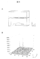
- a schematic diagram (A) showing the structure of two triangular metal thin films and a simulation result (B) of near-field generated in the vicinity of the metal thin films are shown.
- 2 shows a typical Raman scattering spectrum of a nucleobase.
- FIG. 6 is a schematic diagram of a cross section of a nanopore chip of Example 3.
- FIG. 6 is a schematic diagram of a nanopore chip of Example 4.
- FIG. 6 is a schematic diagram of a nanopore chip of Example 5.
- FIG. 6 is a schematic enlarged view of a cross section of a nanopore chip of Example 5.
- the present invention is a device for analyzing characteristics of a biopolymer using nanopores and Raman scattering (preferably tip enhanced Raman scattering: TERS) (hereinafter referred to as “characteristic analysis chip of biopolymer” or “analysis chip of the present invention”). And a biopolymer characteristic analysis apparatus provided with the device, and a method for analyzing the characteristics of the biopolymer using them. Therefore, the biopolymer characteristic analysis chip according to the present invention includes a solid substrate, at least one nanopore provided on the solid substrate, and at least one conductive element disposed on a part of the solid substrate forming the nanopore. A thin film.
- the solid substrate can be formed of an electrical insulator material, for example, an inorganic material and an organic material (including a polymer material).
- the electrical insulator material include silicon, glass, quartz, polydimethylsiloxane (PDMS), polytetrafluoroethylene (PTFE), polystyrene, and polypropylene.
- the size and thickness of the solid substrate are not particularly limited as long as nanopores can be provided, and are compatible with the components (detectors, etc.) of the analysis apparatus used when analyzing the biopolymer described later. Adjust to.
- the solid substrate can be produced by a method known in the art, or can be obtained as a commercial product.
- the solid substrate can be fabricated using techniques such as photolithography and etching, laser ablation, injection molding, casting, molecular beam epitaxy, chemical vapor deposition (CVD), electron beam or focused ion beam.
- the solid substrate may be coated to avoid adsorption of other molecules to the surface.
- the solid substrate preferably has a thin film portion for providing nanopores. That is, a nanopore can be easily and efficiently formed on a solid substrate by providing a thin film portion having a material and thickness suitable for forming nano-sized pores on the solid substrate.
- a thin film portion may be the same material as the solid substrate or may be formed from another electrical insulator material.
- the material of the thin film portion is preferably, for example, silicon oxide (SiO 2 ), silicon nitride (SiN), silicon oxynitride (SiON), metal oxide, metal silicate, or the like.
- the thin film part (and the whole solid substrate depending on the case) is substantially transparent from the point of the excitation efficiency and the light collection efficiency of the external light mentioned later.
- substantially transparent means that external light can be transmitted through approximately 50% or more, preferably 80% or more.
- the thin film portion may be a single layer or multiple layers, and in the case of multiple layers, a conductive thin film described later may be interposed between the layers of the thin film portion.
- the thickness of the thin film portion of the solid substrate is 10 nm to 200 nm, preferably 15 nm to 100 nm, more preferably 20 nm to 50 nm.
- the thin film portion can be formed on the solid substrate by techniques known in the art, for example, by low pressure chemical vapor deposition (LPCVD).
- LPCVD low pressure chemical vapor deposition
- the solid substrate is provided with at least one nanopore.
- nanopore and “pore” are pores of a nanometer (nm) size, and are pores penetrating the front and back of a solid substrate, preferably a thin film portion of the solid substrate. That is, the analysis chip of the present invention is classified into so-called solid nanopores.
- the “opening” refers to a portion of the pore that is exposed on the surface of the solid substrate.
- the pore size (that is, the opening size) can be selected appropriately depending on the type of biopolymer to be analyzed, and is, for example, 1 nm to 100 nm, preferably 1 nm to 50 nm, specifically 1 nm or more and 2 nm or less, 3 nm to 5 nm, 10 nm to 50 nm, and the like.
- the diameter of ssDNA (single-stranded DNA) is about 1.5 nm, and an appropriate range of the pore diameter for analyzing ssDNA is about 1.5 nm to 10 nm, preferably about 1.5 nm to 2.5 nm.
- the diameter of dsDNA (double-stranded DNA) is about 2.6 nm, and an appropriate range of the pore diameter for analyzing dsDNA is about 3 nm to 10 nm, preferably about 3 nm to 5 nm.
- an appropriate range of the pore diameter for analyzing dsDNA is about 3 nm to 10 nm, preferably about 3 nm to 5 nm.
- a pore diameter corresponding to the outer diameter of the biopolymer can be selected.
- the depth of the nanopore can be adjusted by adjusting the thickness of the solid substrate or the thin film portion of the solid substrate.
- the depth of the nanopore is 2 times or more, preferably 3 times or more, more preferably 5 times or more the monomer unit constituting the biopolymer.
- the depth of the nanopore is preferably 3 or more bases, for example, about 1 nm or more.
- the biopolymer can enter the nanopore while controlling its shape and moving speed, and highly sensitive and highly accurate analysis is possible.
- the pore shape is basically circular, but may be elliptical or polygonal.
- At least one pore can be provided on the solid substrate, and when a plurality of pores are provided, it is preferably arranged regularly.
- the pore is formed on the solid substrate by a method known in the art, for example, by irradiating an electron beam of a transmission electron microscope (TEM), using a nanolithography technique or an ion beam lithography technique. Can do.
- TEM transmission electron microscope
- At least one conductive thin film is disposed on a part of the solid substrate forming the nanopore.
- the portion where the conductive thin film is in contact with the nanopore is not the entire circumference of the nanopore but only a part of the entire circumference for the reason described later.
- the conductive thin film can be formed of a material having conductivity or light scattering characteristics. Such materials include metals such as platinum groups such as platinum, palladium, rhodium and ruthenium, gold, silver, copper, aluminum, nickel and the like; graphite such as graphene (which may be either a single layer or multiple layers). Can be mentioned.
- the conductive thin film is formed in a flat shape as is clear from the definition of the thin film.
- the thickness of the conductive thin film is 0.1 nm to 10 nm, preferably 0.1 nm to 7 nm, depending on the material used. As the thickness of the conductive thin film is smaller, the generated near field can be limited, and analysis with high resolution and high sensitivity becomes possible.
- the size of the conductive thin film is not particularly limited, and can be appropriately selected according to the size of the solid substrate and nanopore used, the wavelength of excitation light used, and the like. If the conductive thin film is not planar and has a bend or the like, a near field is induced at the bend and light energy leaks, and Raman scattered light is generated at an undesired location.
- the conductive thin film is preferably planar, in other words, the cross-sectional shape is preferably linear without bending. Forming the conductive thin film in a planar shape is preferable not only from the viewpoint of reducing the background light and increasing the S / N ratio, but also from the viewpoint of uniformity of the thin film and reproducibility in production.
- the shape of the conductive thin film can be any shape as long as it can generate and enhance a near field by irradiating with external light. Probes that generate such near fields are known in the art, such as shapes with sharp edges that can generate and enhance near fields by tip enhanced Raman scattering (TERS), metal bowtie structures, etc. It has been known.
- TMS tip enhanced Raman scattering
- An example of a preferable planar shape of the conductive thin film is a shape having an acute end, and it is particularly preferable to provide the end facing the nanopore.
- the angle of the end is 10 to 80 degrees, preferably 20 to 60 degrees, and more preferably 20 to 40 degrees.
- a preferable shape of the conductive thin film (light scatterer) for forming such near-field light refer to, for example, JP-A-2009-150899.
- the apex portion of the end portion of the conductive thin film is not necessarily a point in a strict sense, and may be a rounded shape having a radius of curvature of a certain value or less, preferably 10 nm or less.
- the entire shape of the conductive thin film may be any shape as long as it has an acute end, and may be a polygon such as a triangle, a quadrangle, or a pentagon, a sector, or a combined shape of a circle and a triangle. Is possible.
- a metal bow-tie structure as the shape of the conductive thin film. That is, two conductive thin films having a circular shape, an elliptical shape, or a polygonal shape are arranged so that convex portions of the shape face each other. See, for example, US Pat. No. 6,649,894 for such a metal bowtie structure.
- the metal bow tie structure can also be regarded as a structure in which a gap (opening) is inserted in a region where a near field is formed. By inserting a gap, anisotropy is introduced and detection sensitivity is improved. See, eg, US Pat. No. 6,768,556 and US Pat. No. 6,949,732 for a description of such techniques.
- the conductive thin film is provided with a structure such as at least a part thereof, particularly preferably an end portion that generates a near field, facing the nanopore.
- the conductive thin film may be disposed on the surface of the solid substrate, or may be disposed between the solid substrates as long as at least a part thereof, particularly preferably, the end thereof is provided facing the nanopore. Also good. For example, it can be arranged on the surface of the solid substrate facing the opening of the nanopore. Alternatively, the conductive thin film can be disposed at a substantially intermediate position (depth) in the central axis direction of the nanopore on the solid substrate. In this case, the conductive thin film preferably has a structure sandwiched between thin film portions of the solid substrate.
- the near field is formed near the center of the nanopore in the central axis direction (depth direction), so that the Raman scattering light of the biopolymer can be generated in the nanopore while controlling the shape and moving speed of the biopolymer. It is possible to perform analysis with high accuracy and high sensitivity.
- positioning a conductive thin film on a solid substrate it is preferable to arrange
- At least one conductive thin film may be disposed for each nanopore, and may be an odd number or an even number.
- one, two, three, four or more conductive thin films can be placed for each nanopore.
- the conductive thin film may be a single thin film having a plurality of units, with the above-described shape being a unit.
- a specific example can be a thin film structure in which two units are linked as in Example 5.
- the conductive thin film is preferably arranged so that the end thereof faces the opening of the nanopore. More specifically, the conductive thin film is disposed in a plane orthogonal to the nanopore central axis and the end of the thin film faces the opening of the nanopore. When at least two conductive thin films are arranged, it is preferable that these conductive thin films are arranged to face each other across the opening of the nanopore. In such a case, by irradiating the conductive thin film with external light, a near-field is generated at the end of the conductive thin film facing the nanopore, and the Raman scattered light of the biopolymer entering the nanopore is generated.
- the conductive thin film can be produced by a method known in the art and placed on a solid substrate.
- a desired shape can be formed by an electron beam after a silver thin film having a desired thickness is formed on the substrate by sputtering.
- graphene formed from graphite can be placed on a supporting substrate and irradiated with an electron beam to form graphene having a desired shape.
- the biopolymer entering the nanopore is excited to generate Raman scattered light, and the characteristics of the biopolymer can be analyzed based on the spectrum of the Raman scattered light. it can.
- a near field is formed at the end of the conductive thin film facing the opening of the nanopore, and the biopolymer is formed by the near field light. Scan two-dimensionally.
- the thickness of the formed near field is basically the same as the thickness of the conductive thin film, that is, the conductive thin film is orthogonal to the central axis of the nanopore. The thickness of the conductive thin film. Therefore, biopolymers can be analyzed with high spatial resolution and high sensitivity by using the analysis chip of the present invention.
- the present invention also relates to a biopolymer characteristic analysis apparatus (hereinafter also referred to as “analysis apparatus of the present invention”) provided with the above-described analysis chip of the present invention. Therefore, an analysis apparatus according to the present invention includes the analysis chip, a light source, and a one-dimensional or two-dimensional detector having a frame rate of 1 kHz or higher.
- the analysis chip of the present invention is irradiated with external light from the light source, and the Raman scattered light of the biopolymer in the analysis chip is detected using the detector.
- a light source known in the art that emits external light (excitation light) having a wavelength capable of generating Raman scattered light can be used.
- a krypton (Kr) ion laser, a neodymium (Nd) laser, an argon (Ar) ion laser, a YAG laser, a nitrogen laser, a sapphire laser, and the like can be used.
- Irradiate with external light 800 nm, preferably 500 to 600 nm.
- the background signal (background signal)
- it may be combined with a filter, a half mirror, a confocal pin pole, or the like.
- a filter for detecting Raman scattered light
- a half mirror for detecting Raman scattered light
- a confocal pin pole for detecting Raman scattered light
- the generated Raman scattered light may be generated by normal Raman scattering, resonance Raman scattering, tip enhanced Raman scattering (TERS), surface enhanced Raman scattering (SERS), or the like.
- any spectroscopic detector can be used as long as it has a frame rate (operation speed) of 1 kHz or more and can detect Raman scattered light.
- One or more one-dimensional or two-dimensional detectors can be used depending on the number and arrangement of nanopores in the analysis chip to be used. Examples of such a spectroscopic detector include a CCD (Charge Coupled Device) image sensor, a CMOS (Complementary Metal Oxide Semiconductor) image sensor, and an image sensor of other high-sensitivity devices (such as an avalanche photodiode).
- the detector preferably has a photomultiplier mechanism, for example, an image intensifier, in order to prevent a decrease in sensitivity due to an increase in detection speed.
- the detector preferably includes a large-capacity memory that can directly record image information of Raman scattered light, thereby enabling high-speed analysis without going through a cable, board, computer, or the like.
- the analysis apparatus of the present invention preferably further includes a frame buffer memory that records measurement values from the detector.
- the analysis device of the present invention may be connected to an output device (for example, a computer) for digitizing and outputting the measurement value from the detector.
- the analysis apparatus of the present invention preferably includes a mechanism for controlling the moving speed of the biopolymer, that is, a sample moving mechanism.
- the sample moving mechanism for example, causes the monomer in the biopolymer to enter the nanopore of the analysis chip one unit at a time in synchronization with the frame rate of the detector.
- a sample driving device arbitrary function generator, electrode, etc.
- the movement of the biopolymer can be controlled so that the monomer in the biopolymer sequentially enters and leaves the nanopore, and the Raman scattering spectrum corresponding to each monomer (constituent unit) is time-lapsed. Can be obtained.
- a method for controlling the moving speed of the biopolymer there is a method for increasing the viscosity of the sample solution containing the biopolymer.
- the Brownian motion of the biopolymer can be suppressed by controlling the temperature around the analysis chip to lower the temperature of the sample solution and increase the viscosity of the sample solution.
- the viscosity of the sample solution can be increased, and at the same time, the three-dimensional structure of the biopolymer can be linearized.
- the moving speed can be controlled.
- the second polymer preferably, a polymer having a size larger than the inner diameter of the nanopore, more preferably a polymer cross-linked three-dimensionally, the second polymer can enter the nanopore. This makes it possible to eliminate Raman scattering caused by the second polymer that is not a measurement target.
- Another method of controlling the moving speed of the biopolymer is a method of applying a pressure difference to each sample solution existing at the upper part and the lower part of the analysis chip of the present invention.
- the main axis of the biopolymer and the central axis of the nanopore substantially coincide.
- the biopolymer passes through the nanopore, and the unit elements (monomer) constituting the biopolymer sequentially pass through the near field formed on the analysis chip. That is, the monomers arranged along the principal axis direction of the polymer are sequentially exposed to the near field and absorb light to generate Raman scattered light.
- Raman scattering spectra derived from the monomers can be sequentially obtained.
- biopolymer characteristic analysis can be performed using the above-described biopolymer characteristic analysis chip or characteristic analysis apparatus of the present invention.
- the “biopolymer” refers to a multimer (oligomer) or polymer (polymer) in which a plurality of small molecules (monomer, monomer) having a unit structure are linked, and a living body and a living body. It means something derived from something.
- nucleic acids such as single-stranded DNA (ssDNA) and double-stranded DNA (dsDNA), single-stranded RNA (ssRNA) and double-stranded RNA (dsRNA), and hybrid nucleic acids composed of DNA and RNA; Peptide nucleic acids; proteins and peptides such as proteins and peptides consisting of D- and L-amino acids; sugar chains such as polysaccharides, sugar chains in glycoproteins; aptamers such as RNA aptamers and the like.
- Biopolymers include polymers that contain sequences and components that do not exist in nature, such as sequences such as poly (A), poly (T), poly (G), poly (C), etc.
- Biopolymers also include nucleic acids prepared by nucleic acid amplification techniques known in the art (eg, polymerase chain reaction) and nucleic acids cloned into vectors. Methods for preparing samples containing these biopolymers are well known in the art, and those skilled in the art can appropriately select a preparation method according to the type of biopolymer.
- “analysis” refers to characteristic analysis of a biopolymer.
- “analysis” refers to analyzing the sequence order of monomers that are units constituting a biopolymer, for example, analyzing the base sequence of a nucleic acid.
- the spectral spectrum of each monomer that constitutes the biopolymer is measured. The monomer is qualitatively (identified) based on a comparison with the above.
- Raman scattered light of the monomer constituting the biopolymer is sequentially obtained, the obtained Raman scattering spectrum is compared with the standard spectrum, the qualitative (ie, type) of the monomer is determined, and these steps are By sequentially executing sequentially, it is possible to determine the order in which monomers are arranged in the biopolymer, that is, to perform sequence analysis.
- FIG. 1 is a schematic diagram of a nanopore chip 100 for biopolymer characteristic analysis of this example.
- the nanopore chip 100 includes a substrate 110, a nanopore 120, a conductive thin film 130, and the like.
- a plane parallel to the widest surface of the substrate 110 (hereinafter referred to as the substrate surface) is defined as an xy plane
- a direction connecting the conductive thin film 130 and the nanopore 120 is defined as an x axis
- a direction perpendicular to the xy plane is defined as a z axis.
- the nanopore 120 is formed substantially perpendicular to the substrate surface. In other words, the central axis of the nanopore is parallel to the z-axis.
- FIG. 2 is a schematic enlarged view of the xz cross section including the central axis 121 of the nanopore 120 of the nanopore chip 100 of the present embodiment.
- the substrate 110 has a thin film portion 111 on the substrate surface above the z axis, and further has a conductive thin film 130 thereabove.
- the substrate has a tapered recess (hereinafter referred to as “window portion 112”) below the z-axis, and the thin film portion 111 of the substrate is exposed there.
- Nanopores 120 are formed in the thin film portion 111 of the window 112.
- one end 131 of the conductive thin film 130 faces the upper end of the opening of the nanopore 120.
- the planar shape of the end 131 is a sharp end, and the sharp end faces the nanopore 120.
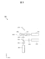
- FIG. 3 is a schematic configuration diagram of the biopolymer characteristic analysis apparatus 200 according to this embodiment.
- the analysis device 200 includes a light source 210, a lens 220, a half mirror 230, an objective lens 240, a filter 250, a spectroscopic detector 260, a terminal 270, an xyz fine movement stage 600, a sample driving device 700, a sample cell 300, and a measurement control device such as a personal computer. (Not shown).
- a nanopore chip 100 is accommodated in the sample cell 300.
- FIG. 4 is an xz cross-sectional view showing a schematic configuration of the sample cell 300.
- the sample cell 300 includes a nanopore chip 100, an upper member 310, a lower member 320, screws (not shown), and the like.
- the lower member 320 includes an O-ring 330, sample channels 410, 420, and 430, a sample chamber 440, and an electrode chamber 450 formed therein, a sample connection port 460 and 470, and an electrode connection port 480. Is formed.
- a sample feeding tube (not shown) is airtightly connected to the lower member 320 via the sample connection ports 460 and 470, and a silver-silver chloride electrode (not shown) is airtightly connected via the electrode connection port 480. Is done.
- the silver chloride electrode having a silver chloride end is accommodated in an electrode chamber 450 (not shown), and the silver end (hereinafter, silver end) is exposed to the outside of the electrode connection port 480.
- Sample feeding tube, sample connection port 460, sample channel 410, sample chamber 440, sample channel 420, electrode chamber 450, sample channel 430, sample connection port 470, sample solution tube Is filled with a sample solution (not shown) without any gaps (without the inclusion of bubbles). Therefore, the sample solution in the sample chamber 440 comes into contact with the silver-silver chloride electrode in the electrode chamber 450, and both are electrochemically connected.
- the upper member 310 is the same as the lower member 320.
- the sample cell 300 is prepared. Specifically, the nanopore chip 100 is sandwiched between the upper member 310 and the lower member 320 by the O-ring 330 to form the upper and lower sample chambers 540 and 440 in an airtight manner. A 100 mM KCl aqueous solution is introduced as a sample solution from the sample feeding tube, and the sample chambers 540 and 440 and the electrode chamber 450 are filled with the sample solution.
- the sample cell 300 is installed in the analyzer 200. Specifically, the sample cell 300 is fixed to the fine movement stage 600. Using the fine movement stage 600 and a visual optical system (not shown), the optical system is focused on the thin film portion 111 of the nanopore chip 100 in the sample cell 300. Two silver-silver chloride electrodes installed in the sample cell 300 are connected to the sample driving device 700.
- the sample driving device 700 has a built-in voltage source or current source, and can apply a voltage to the lower sample chamber 440 using the upper sample chamber 540 as a reference.
- the optical system of the analyzer operates as follows. Specifically, the laser light emitted from the light source 210 is shaped through the lens 220, reflected by the half mirror 230, and condensed on the thin film portion 111 of the nanopore chip 100 by the objective lens 240. The laser light passes through the thin film portion 111 and irradiates the conductive thin film 130, and strong near-field light is generated at the end 131 (facing the opening of the nanopore 120).
- a chemical substance biological polymer
- the near-field light excites the chemical substance and generates Raman scattering light peculiar to the chemical substance.
- the Raman scattered light is collected by the objective lens 240, passes through the half mirror 230, the Rayleigh scattered light and the anti-Stokes line are removed by the filter 250, and the Stokes line of the Raman scattered light is incident on the spectroscopic detector 260.
- the Raman scattering spectrum (of the Stokes line) is spectroscopically detected.
- the light that has passed through the thin film portion 111 and the conductive thin film 130 is absorbed by the terminal 270 or diffused in an unrelated direction.
- the main optical path is indicated by a broken line in FIG.
- the DNA measurement procedure is as follows. That is, for example, a sample in which a single-stranded DNA having a length of 10 kb (knt) was dissolved in a 100 mM KCl aqueous solution to a concentration of 1 nM was used. This is introduced into the sample chamber 440 as a lower sample solution. When a negative voltage of 100 mV is applied to the lower sample chamber 440 using the sample driving device 700, ions in the sample solution are electrophoresed through the nanopore 120, and a current (ion current) flows. Since only near water and KCl exist in the near field, the Raman scattering spectrum of only water is observed.
- DNA is electrophoresed from the lower sample chamber 440 through the nanopore 120 to the upper sample chamber 540 by electrophoresis.
- the nucleobase that is a constituent element of the DNA enters the near field formed at the end 131 of the conductive thin film 130.
- Raman scattered light peculiar to the base is generated, and the Raman scattered spectrum is acquired by the spectroscopic detector 260.
- the nucleobases move and leave the near field.
- the Raman scattered light peculiar to the base disappears.
- the electrophoresis is further continued, the next base on the DNA sequence similarly enters and exits the near field sequentially, and the Raman scattering spectrum corresponding to the base sequence is acquired over time.
- the scattered light intensity at the wave number characteristic for each base (hereinafter referred to as the characteristic band) is acquired over time, and the time variation is used to reduce the spectral information for each base using the difference method described in Non-Patent Document 3, etc. By analyzing, the base sequence of DNA is obtained.
- the characteristic band The scattered light intensity at the wave number characteristic for each base
- the time variation is used to reduce the spectral information for each base using the difference method described in Non-Patent Document 3, etc.
- the base sequence of DNA is obtained. The above is the outline of the operation of the present embodiment.
- the nanopore chip 100 in this example was manufactured by the following procedure.
- a silicon substrate was used as the substrate 110, and an oxide film having a thickness of about 20 nm was formed on the surface by LPCVD (low pressure chemical vapor deposition) (this oxide film finally becomes the thin film portion 111).
- a window pattern is formed on the bottom of the substrate by electron beam (EB) lithography, the surface layer is removed by reactive ion etching, and then silicon is removed by KOH (potassium hydroxide) wet etching.
- a window portion 112 having the same was formed.
- As the conductive thin film 130 a silver thin film was formed on the substrate surface by sputtering. The film thickness of silver was about 5 nm.
- a resist was applied on the silver thin film, the triangular pattern shown in FIG. 1 was formed by EB lithography, and the silver other than the triangular pattern was removed by etching to remove the resist. Finally, the substrate was observed with a transmission electron microscope (TEM), and a nanopore 120 was formed by irradiating the triangular end portion 131 with a TEM electron beam. The inner diameter of the nanopore was about 10 nm.
- the thin film portion 111 is formed using silicon oxide, but silicon nitride or the like can be used similarly.
- the shape of the conductive thin film 130 in this example is a triangle, and the angle of the apex of the end 131 is 30 degrees, and the length of the triangle in the x direction is the wavelength of excitation light (531 nm) described later. A sufficiently short 100 nm was adopted.
- the preferable shape of the conductive thin film (scattering body) for forming near-field light is described in detail in Japanese Patent Application Laid-Open No. 2009-150899 (hereinafter also referred to as “fourth conventional example”).
- the shape of the thin film 130 can also be selected according to the fourth conventional example.
- the angle of the apex of the end 131 when the angle of the apex of the end 131 is smaller (a sharp angle), charges are more likely to concentrate on the end, and the near-field enhancement effect is higher.
- the end portion other than the end portion 131 hereinafter, the other end portion
- the near-field light formed at the other end portion Not affected. Therefore, the appropriate value of the vertex angle can be expanded in a direction smaller than that in the fourth conventional example.
- this angle is too small, the area of the conductive thin film decreases, and the efficiency of utilization of incident light energy decreases. Accordingly, an angle of 10 to 80 degrees, more preferably 20 to 60 degrees can be suitably employed as the vertex angle.
- the apex portion of the triangular end 131 does not have to be a point in a strict sense, and has a rounded shape or the like having a radius of curvature of a certain value, preferably 10 nm or less. There may be.
- the angles other than the triangular end portion 131 are preferably obtuse than the end 131 angle.
- the shape of the conductive thin film 130 is not limited to a triangle, and it is only necessary to have the end portion 131 whose apex angle is an acute angle as described above, and the shape of the other portion may be a circle without a corner or a corner.
- the shape of the conductive thin film 130 can be selected from various shapes such as a sector shape, a combined shape of a circle and a triangle, a polygon such as a triangle, a quadrangle, and a pentagon. Further, in this embodiment, even if near-field light is formed in the region shielded by the substrate 110, it does not affect the measurement. Therefore, the shape of the conductive thin film in the shield region can be freely selected.
- a transparent member is used in the sample cell 300, particularly in the central portion of the upper member 310 and the lower member 320 (part separating the sample chambers 440 and 540 from the outside).
- transparent members that can be used include glass, quartz, and plastic materials such as acrylic that are highly transparent at the light source wavelength.
- the laser light emitted from the light source 210 is reflected by the half mirror 230 and then is incident in a direction substantially perpendicular to the nanopore chip 100. It is preferable to tilt the incident angle of the laser light with respect to the normal line of the nanopore chip 100. Further, in FIG. 3, for the sake of simplicity, nothing is installed between the objective lens 240 and the nanopore chip 100, but it is illustrated as appropriate at an appropriate position between the objective lens 240 and the nanopore chip 100. It is preferable to provide a slit having a simple shape. By adopting these configurations, it is possible to avoid the problem that the reflected light from the nanopore thin film portion 111 enters the spectroscopic detector 260, suppress the background light, and obtain a high S / N.
- the objective lens 240 and the sample cell 300 are illustrated as being slightly separated from each other. However, in an actual apparatus, it is desirable that both be as close as possible.
- the distance between the objective lens 240 and the nanopore chip 100 is preferably 3 mm or less, preferably 1 mm or less. Thereby, the excitation efficiency by excitation light and the condensing efficiency of scattered light can be raised, and highly sensitive measurement can be performed.
- the objective lens 240 is preferably an immersion type.
- the objective lens preferably has a high aperture, and numerical aperture ⁇ 0.8 is particularly good.
- the biopolymer characteristic analysis apparatus in this example was constructed based on a microscope-integrated laser Raman spectroscopic apparatus similar to the third conventional example. However, the stage attached to the microscope was used as the xyz fine movement stage 600, and the piezo stage for AFM was not used.
- a Kr ion laser with an output of 1 mW and a wavelength of 531 nm was used as the light source 210. The laser and its wavelength can be appropriately selected.
- An arbitrary function generator was used as the sample driving device 700, and an arbitrary function generator was used in combination with an attenuator (resistance voltage divider) as necessary.
- the sample driving device 700 can output DC having an output voltage range of 0 to ⁇ 10 V or an arbitrary waveform.
- a typical example of the arbitrary waveform is a pulse wave.
- the pulse peak time width is in units of 10 nanoseconds, and the voltage value of the pulse peak can be arbitrarily output within the aforementioned output voltage range.
- the substrate 110 of the nanopore chip 100 is mainly formed of silicon (Si).
- the thickness of the substrate is about 700 ⁇ m.
- the thin film portion 111 of the substrate is made of silicon oxide (SiO 2 ) and is as thin as about 20 nm. Accordingly, in the window portion 112 of the substrate, the laser light passes through the thin film portion 111 and irradiates the conductive thin film 130. By irradiating the conductive thin film 130 with laser light, a strong near field is generated at the end 131 thereof. It is preferable to use a laser beam polarized in the direction toward the tip of the end, that is, in the x-axis direction. The thickness of the near field in the z direction is about the same as the thickness of the conductive thin film 130, that is, about 5 to 10 nm.
- the substrate 110 has a thickness of about 700 ⁇ m. Since Si, which is the material of the substrate 110, absorbs, reflects, and scatters laser light, the laser light is applied to the thin film portion 111 formed on the region other than the window portion 112 and the conductive thin film 130 formed thereon. Hardly reach. Therefore, the formation of the near field in the conductive thin film 130 is suppressed in the region other than the window 112. In other words, with the above configuration, the formation of the near field in the conductive thin film 130 can be mainly limited to the region of the window 112, particularly the target end 131, and the generation of background light in regions other than the target can be suppressed. There are features.
- an antireflection treatment to the surface of the substrate 110 in a region other than the window 112, specifically, for example, to make it rough or to apply a light-absorbing material.
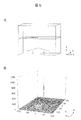
- the near-field light distribution generated in the vicinity thereof was calculated using the FTDT method (time domain light propagation solver OptiFDTD, “Optiwave System Inc.”).
- the size of the analysis region is set to 0.3 ⁇ 0.2 ⁇ 2.6 um in the X, Y, and Z directions (X, Y, and Z are coordinate systems used only in FIGS. 5 and 6).
- Y is the direction perpendicular to the XZ plane).
- the conductor material was silver, the thickness was 10 nm, and the tip angle was 90 degrees.
- the polarization direction of the incident wave was the X direction.
- the boundary conditions are the periodic boundary condition on the XY side and the absorbing boundary condition on the Z side.
- the mesh size was uniformly 2.6 nm over the entire calculation region.
- FIG. 5A is a schematic diagram of the analyzed structure.
- FIG. 5B the XY plane distribution of the ratio between the calculation result of the near-field intensity density (I) and the intensity density (Iin) of the incident wave is plotted on the vertical axis. As shown in the figure, the strongest light field was generated at the tip of the thin film triangle, and the maximum value was about 1100 times the incident intensity ratio.
- the absolute value of the voltage applied to the lower sample chamber 440 is reduced using the sample driving device 700, and DNA electrophoresis is performed. The speed can be reduced.
- the DNA strand can be migrated in the reverse direction at a low speed. By migrating until no Raman scattered light derived from the base is observed under these conditions, the tip of the DNA strand can be pushed back out of the near field.
- the voltage polarity is restored while the absolute value of the applied voltage is reduced (the lower sample chamber 440 is set as a negative voltage), so that the electrophoresis slowly starts from the top of the DNA strand and repeats the Raman scattering measurement. It is possible. As a result, the base to be measured can be kept in the near field for the time required to measure the Raman scattering spectrum with sufficient accuracy.
- the average moving speed of the DNA strand can be adjusted (low) with extremely high resolution according to the duty ratio. Further, by combining with the adjustment of the pulse wave height (pulse height modulation), it is possible to adjust the migration speed more precisely.
- the electrophoretic voltage and its pulse width By controlling the electrophoretic voltage and its pulse width, the base to be measured can be kept in the near field for the time required to measure the Raman scattering spectrum with sufficient accuracy.
- the Raman scattering spectrum within the stop time it is possible to avoid the inconvenience that the signal fluctuates due to the measurement target entering or leaving the near field during measurement, and to improve the measurement value. Is possible.
- the voltage applied to the lower sample chamber 440 can be periodically repeated between a positive pressure and a negative pressure. At this time, by adjusting the time-averaged voltage to be slightly negative, the DNA strand is stretched more stably and slowly through the nanopore 120 than when the voltage is simply set to a constant negative pressure. The sample can be migrated to the sample chamber 540, and Raman scattering based on individual bases in the DNA strand can be measured with high sensitivity.
- the sample solution As another means for controlling the migration rate of the DNA strand, it is effective to increase the viscosity of the sample solution. Adding a mechanism to control the temperature around the nanopore chip and lowering the temperature of the sample solution will increase the viscosity of the sample solution and at the same time suppress the Brownian motion of the DNA strand, making it good for Raman scattering measurement of the DNA strand It becomes a condition.
- the sample solution can be made more viscous, and at the same time the three-dimensional structure of the DNA strand can be made linear, which is good for Raman scattering measurement of the DNA strand. It becomes a condition.
- a separation medium for capillary electrophoresis may be used.
- a polymer that is preferably larger than the inner diameter of the nanopore, more preferably three-dimensionally cross-linked only the viscosity can be increased without disturbing the measurement.
- the enhancement field that is, the measurement region inside the nanopore.
- the non-measurement polymer does not enter the measurement region, and the measurement target biological polymer. For example, it is possible to allow only a DNA strand to enter the measurement region, and it is possible to eliminate Raman scattering caused by a polymer not to be measured.
- the existing pair of silver-silver chloride electrodes are regarded as the sample electrode and the counter electrode, respectively, and a reference electrode is newly provided in the sample chambers 440 and 540 on the counter electrode side, and the voltage between the sample electrode and the reference electrode is set.
- the current flowing between the sample electrode and the counter electrode can be controlled so as to be a value.
- a predetermined minute voltage can be accurately applied between the upper and lower sample chambers 440 and 540, a minute migration speed can be realized, and it can be accurately controlled.
- a galvanostat method can be adopted.
- the existing pair of silver-silver chloride electrodes can be regarded as a sample electrode and a counter electrode, respectively, and feedback control can be performed so that a predetermined value is obtained while monitoring the current flowing from one to the other.
- a predetermined minute current can be accurately passed between the upper and lower sample chambers 440 and 540, and a minute migration speed can be realized and controlled accurately.
- a fifth method it is possible to adopt a method in which a nanopore substrate is made using a semiconductor doped with an impurity, thereby making the nanopore substrate conductive and controlling the potential of the nanopore substrate surface. By using a potentiostat or the like, it is possible to control the potential of the nanopore substrate surface with respect to the potential in the liquid.
- a further method for controlling the speed at which the DNA strand passes through the nanopore 120 will be described.
- the force that causes the DNA strand to pass through the nanopore by electrophoresis and the opposite force Can be added to the DNA strand, the rate at which the DNA strand passes through the nanopore can be reduced.
- the upper sample chamber A pressure in the direction from 540 toward the lower sample chamber 440 can be generated.
- This pressure difference may be controlled by an osmotic pressure based on a composition difference between the upper and lower sample solutions, for example, an ion concentration difference.
- This pressure difference causes the sample solution to flow in bulk in the nanopore 120 in the direction opposite to the DNA strand electrophoresis, that is, in the direction from the upper sample chamber 540 to the lower sample chamber 440.
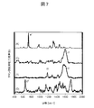
- FIG. 8 is an output screen display image of the PC corresponding to this procedure.
- the spectrum information for each base obtained as a result of the difference method is displayed for each feature band a1, t1, g1, c1, t2 with the horizontal axis: time and the vertical axis: signal intensity (wave number). . Since the feature bands c1 and t2 overlap as described above, the wave number range c1 to t2 including both is displayed.
- the determined sequence is displayed at the top of the screen, stored in the PC, and output as a result.
- RNA can be analyzed by analyzing the spectrum of U.
- DNA methylation can be read directly.
- obtaining a spectrum of amino acids it is possible to analyze peptides and proteins, and it is also possible to analyze sugar chains by obtaining spectra of sugars.
- the biopolymer characteristic analysis chip according to this example is based on solid nanopores, and thus has a feature of high structural stability and high reliability.
- the type of monomer is determined using the Raman spectrum as an index. Since the spectrum has two-dimensional information called intensity patterns with respect to wave numbers, the amount of information is dramatically higher than that of one-dimensional information such as tunnel current intensity, and the qualitative discrimination ability is high, thus the base discrimination ability is high.
- the near field was fixed to the opening of the nanopore 120, and the sample driving device 700 was used to migrate DNA and control the relative positional relationship with the near field.
- FIG. 9 is a schematic diagram of a nanopore chip 100a according to this modification.
- the nanopore chip 100a includes a substrate 110, a nanopore 120, conductive thin films 130a and 130b, and the like. That is, two conductive thin films corresponding to the conductive thin film 130 in Example 1 were provided, one of them (conductive thin films 130a and 130b) was rotated 180 degrees, and the ends were arranged facing the nanopores. However, this is different from the first embodiment.
- FIG. 10 is a schematic enlarged view of the xz cross section including the central axis 121 of the nanopore 120 of the nanopore chip 100a of this modification.
- the conductive thin films 130a and 130b are formed above the z-axis of the thin film portion 111, and their end portions 131a and 131b face the upper ends of the openings of the nanopore 120 and face each other. That is, the conductive thin films 130a and 130b are installed at a distance substantially the same as the pore diameter of the nanopore 120.
- the analysis device and operation for the nanopore chip 100a according to this modification are the same as those in the first embodiment.
- the difference is that near-field light generated by laser light irradiation is generated in the gap between the end portions 131a and 131b of the conductive thin films 130a and 130b.
- near-field light derived from both conductive thin films strengthens each other, and the near-field intensity is enhanced.
- the presence of the conductive thin films 130a and 130b limits the distribution of the near field in the x direction, and is limited to about the pore diameter of the nanopore 120.
- the near-field shape of this modification has high symmetry and therefore high uniformity.
- the near field intensity is about 7,000 times as high as the incident light intensity ratio as described above (FIG. 6)
- this modified example has high sensitivity, the near field is spatially uniform, and the spatial resolution is high. There are features.
- a configuration using three or more conductive thin films can be employed.
- the conductive thin film is arranged with a rotational symmetry of 90 degrees about the central axis, if the laser light is incident in the direction of the central axis, the orientation of the laser polarization in the xy direction is not controlled.
- a strong near field can be induced at either end of a pair of conductive thin films facing each other.
- FIG. 11 is a schematic diagram of a multi-nanopore chip 1100 for analyzing biopolymer characteristics according to the second embodiment.
- the multi-nanopore chip 1100 includes a substrate 1110, nanopores 1120 and 1121, conductive thin films 1130a, 1130b, 1131a, 1131b, and the like.
- the multi-nanopore chip 1100 of the present example has a plurality of unit structures of the above-described modified example composed of nanopores and opposing conductive thin films, that is, a unit structure illustrated in FIG.
- FIG. 12 is a schematic configuration diagram of a multi-analysis apparatus 2000 that performs biopolymer characteristic analysis of the second embodiment.
- Multi-analyzer 2000 includes light source 210, lens 220, half mirror 230, objective lens 240, filter 250, prism 2261, imaging lens 2262, two-dimensional detector 2263, termination 270, xyz fine movement stage 600, sample driving device 700, It comprises a sample cell 300, a measurement control device (not shown) such as a personal computer.
- a multi-nanopore chip 1100 is accommodated in the sample cell 300.
- the operation of the second embodiment is the same as that of the first embodiment, but a multi-nanopore chip 1100 having a plurality of unit structures is used as the nanopore chip. Accordingly, Raman scattered light derived from the sample is independently generated at a plurality of locations on the multi-nanopore chip 1100. This Raman scattered light is collected by the objective lens 240, passes through the half mirror 230, and after the Rayleigh scattered light is removed by the filter 250, it is spectralized by the prism 2261, and the two-dimensional detector 2263 is used by the imaging lens 2262. An image is formed on the detection surface.
- the Rayleigh line dispersed by the prism 2261 is refracted in the direction of the z ′ axis in FIG.
- Rayleigh scattered light from the nanopore opening of each unit structure in the x-axis direction and y-axis direction on the multi-nanopore chip 1100 is coupled in the x′-axis direction and y′-axis direction on the detection surface of the two-dimensional detector 2263, respectively.
- the Raman scattered light (Stokes line) is dispersed in the x′-axis direction by the action of the prism 2261. Wavelength dispersion is performed so that the relatively intense Raman line (Stokes line, Raman shift approx.
- the Raman scattered light derived from the nanopores of each unit structure can be two-dimensionally developed without overlapping on the detection surface of the two-dimensional detector 2263 and acquired simultaneously.
- a filter with a bandpass filter is used to eliminate unnecessary light such as the Raman line of water in advance, and to achieve the desired Raman line. Can be two-dimensionally developed without overlapping on the detection surface of the two-dimensional detector 2263 and acquired simultaneously.
- a large number of nanopores were regularly arranged in a lattice pattern on the substrate 1100 in the x and y directions.
- the direction on the detection surface in the x direction which is one of the directions, the wavelength dispersion direction, and one direction of the pixel array of the two-dimensional detector are matched (x ′ direction).
- dx ⁇ dy where dx is the arrangement interval in the x direction of many nanopores on the substrate 1100 and dy is the arrangement interval in the y direction.
- the installation position of the multi-nanopore chip 1100 with respect to the central axis of the optical system can vary from measurement to measurement, the relationship between the pixel coordinates and wavelength, that is, wavelength calibration, must be performed from the position on the detection surface for each nanopore each time. There is. Therefore, prior to the measurement of the Raman scattering spectrum of the polymer to be measured, the scattering spectrum of the sample solution that does not include the measurement object, that is, the reference solution was obtained. Since the composition of the reference solution is known in advance, wavelength calibration can be performed for each nanopore based on the result.
- wavelength calibration was performed from the chromatic dispersion per unit pixel on the basis of the detection pixel coordinates of Raman scattering of water or Rayleigh scattering of water. If Rayleigh scattering is blocked by the filter and cannot be detected, the filter may be removed only at this time. By this step, the light detection result obtained at each nanopore can be converted into a Raman scattering spectrum. At this time, if a process of subtracting the scattering spectrum of the reference solution is performed, a net Raman scattering spectrum to be measured can be obtained, so that a more accurate analysis can be performed.
- the Raman scattering spectrum of the polymer to be measured may be acquired for all the obtainable wavelength regions, but if it is acquired only in the wavelength region necessary for base identification, that is, limited to a specific pixel region, the detection speed In addition to speeding up, it is possible to reduce the amount of data thereafter.
- DNA strands that pass through nanopores by electrophoresis are generally high speed.
- the nanopore passage time of a single-stranded DNA with a base length of 10 kb (knt) is about 1 ms
- the enhancement field residence time per base Is only 0.1 ⁇ s. Therefore, in order to measure the Raman scattering signal from each base independently under these conditions, the operation speed of the two-dimensional detector 2263 needs to be 1 MHz or more.
- the detector operating speed (frame rate) is usually 30 Hz or less. Especially at a fast speed is less than 1KHz. Therefore, the operation speed (frame rate) of the detector is set to 1 KHz or more, preferably 1 MHz, which is a new problem caused by combining the nanopore and the Raman scattering spectrum measurement of the DNA strand passing therethrough in the present invention.
- CMOS complementary metal oxide semiconductor
- CCD charge coupled device
- the CCD performs AD conversion in units of one detection element or one column, whereas in CMOS, AD conversion can be performed simultaneously for all detection elements arranged in a two-dimensional form, and the time required for AD conversion is several times. This is because it can be shortened by one hundred to several thousand times. The same effect can be obtained as long as the detector has an AD conversion function for each detection element, not limited to CMOS. Also, in order to reduce the time required to transfer a large amount of signals acquired by the detector to the control computer via a cable or board and write it to the internal hard disk, etc., a large-capacity memory must be built in the detector. Therefore, it is also effective to store a large amount of signals without going through the above.
- the prism 2261 is used as the wavelength dispersion means for obtaining the Raman scattering spectrum, but a diffraction grating can also be used to increase the resolution of wavelength dispersion. This makes it possible to identify the base species with higher accuracy.
- Raman scattering spectra can be simultaneously obtained for a plurality of nanopores, so that the multiplicity of measurement is high and the result is highly reliable. It has the advantage of high throughput when performing measurements with high multiplicity.
- this modification has a feature that throughput is high because a plurality of samples can be measured in parallel.
- FIG. 13 is a schematic enlarged view of the xz cross section including the central axis 121 of the nanopore 120 of the nanopore chip 100b of the third embodiment.
- the substrate 110 has a thin film portion 111a on the substrate surface above the z-axis, has conductive thin films 130a and 130b thereon, and further has a thin film portion 111b thereon.
- Others are the same as the modified example (FIG. 10) of the first embodiment.
- Nanopoachippu 100b of the third embodiment is similar to Embodiment 1 (Modification), conductive thin film 130a, a pattern of 130b after formation by EB lithography, of SiO 2 having a thickness of about 20nm
- the thin film portion 111b to be formed is formed by sputtering, and then nanopores are formed by TEM. Since the thin film portion 111b is thin, the appearance of the nanopore chip 100b is the same as that of the first embodiment (modified example thereof), that is, as shown in FIG.
- the operation of the third embodiment is the same as that of the first embodiment (modified example thereof), except for the following points.
- the conductive thin films 130a and 130b are covered with the thin film portion 111b, the near field capable of interacting with the sample is localized inside the nanopore 120.
- the remaining near field is confined in the thin film portion 111a and the thin film portion 111b, and thus cannot interact with the sample containing the biopolymer. Therefore, there is a feature that a background signal from a sample existing in a space other than the inside of the target nanopore 120 does not occur and the S / N is high.
- the material of the thin film portion 111b is made of SiO 2 and formed by sputtering, but the material and forming method of the thin film portion 111b are not limited to the above.
- the material of the thin film portion 111b various non-conductive materials can be adopted, and they can be formed by an appropriate surface coating method, whereby the same effect can be obtained.
- the near field is formed just near the center of the nanopore 120 in the central axis direction, the movement of the sample biopolymer such as DNA in the xy direction is limited by the nanopore, so the sample is evenly adjacent. Since it can interact with the field, it has the feature that the reproducibility of the obtained signal is high.
- Nanopore chip for energizing a conductive thin film An example of the structure of a nanopore chip for biopolymer property analysis according to the present invention will be described with reference to FIG.
- FIG. 14 is a schematic diagram of a nanopore chip 100c for biopolymer characteristic analysis of Example 4.
- the nanopore chip 100c includes a substrate 110, a nanopore 120, conductive thin films 130a and 130b, wiring patterns 132a and 132b, contacts 133a and 133b, and the like.
- the wiring patterns 132a and 132b and the contacts 133a and 133b are electrically connected to the conductive thin films 130a and 130b, respectively.
- the wiring patterns 132a and 132b and the contacts 133a and 133b were formed in the same manner as the conductive thin films 130a and 130b in the above-described embodiment. The difference is that gold is used as the material for the wiring pattern and contacts, and the thickness of the wiring pattern is 1 micron and the contact is 100 microns.
- the biopolymer characteristic analysis apparatus according to Example 4 is the same as that of Examples 1 to 3, except for the following points. That is, in Example 4, the contacts 133a and 133b were connected to the second voltage output of the sample driving device 700 through a card edge connector (not shown) so as to have an opposite phase.
- Example 4 the biopolymer was migrated through the nanopore 120 by applying a pulsed voltage from the sample driving device 700 to the sample chamber. Further, a near field was formed at the ends of the conductive thin films 130a and 130b by laser irradiation.
- the pulse of the sample driving device 700 is OFF, the electrophoretic voltage is released, and the contact 133a, 133b is applied with an opposite phase, that is, an ON pulse.
- This pulse voltage is applied to the conductive thin film 130a through the wiring patterns 132a, 132b. , 130b and applied to the end portions 131a, 131b (not shown).
- the phosphate group of DNA which is a biopolymer
- the phosphate group of DNA which is a biopolymer
- DNA migration is temporarily forcibly stopped.
- the Raman scattering spectrum of the biopolymer is acquired.
- an electrophoresis voltage is applied, and an anti-phase, that is, an OFF pulse is applied to the contacts 133a and 133b, and the temporary forced stop of DNA migration is released. Therefore, DNA migration resumes. During this time, no Raman scattering spectrum is acquired.
- FIG. 15 is a schematic diagram of the nanopore chip 100d of the fifth embodiment.
- the nanopore chip 100d includes a substrate 110, a nanopore 120, conductive thin films 130c and 130d, and the like.
- the fifth embodiment is similar to the third embodiment, except for the following points.
- the conductive thin films 130c and 130d single layer graphite, that is, graphene was used.
- the planar shapes of the conductive thin films 130c and 130d are connected to each other so as to surround the periphery by a frame-like structure.
- the conductive thin films 130c and 130d are a single thin film structure having the gaps 134a and 134b.
- the voids 134a and 134b are also connected to each other at the nanopore 120).
- the nanopore 120 has a diameter of 2 nm. The distance between the frame-like structure and the nanopore 120 was set to be a distance that is equal to or slightly longer than the plasmon attenuation distance. In this way, by setting the lengths of the two conductive thin films 130c and 130d to the same distance as the plasmon attenuation distance, the plasmons generated in the conductive thin films 130c and 130d can sufficiently reach the vicinity of the nanopore.
- FIG. 16 is a schematic enlarged view of the xz cross section including the central axis 121 of the nanopore 120. Since the enlargement ratio is high, the outer frame of the conductive thin films 130c and 130d is not shown.
- the fabrication method of the nanopore chip 100d of the fifth embodiment is similar to that of the third embodiment, but the process after the thin film portion 111a is formed on the substrate 110 is different. That is, separately, a graphene was prepared from graphite using a mechanical peeling method, and it was confirmed by an optical microscope that it was a single layer. The graphene was transferred onto a working support substrate using the wedging method described by Schneider et al., Nano Letters (2010) 10 , 1912. Using a high-focus TEM (acceleration voltage 300 kV), the support substrate and the graphene were irradiated with an electron beam to punch out carbon, thereby forming gaps 134a and 134b and connecting portions thereof.
- a high-focus TEM acceleration voltage 300 kV
- the support substrate was taken out of the TEM, and the graphene subjected to the above processing was transferred onto the thin film portion 111a of the substrate 110 using the wedging method again. Thereafter, in the same manner as in Example 3, the thin film portion 111b was formed by sputtering, and the nanopore 120 was formed using TEM (irradiating the electron beam to the connecting portion of the gaps 134a and 134b).
- the two conductive thin films 130c and 130d connected to the frame an extremely narrow gap between them and the complicated shapes of the gaps 134a and 134b can be easily formed with good reproducibility. .
- the operation of the fifth embodiment is the same as that of the third embodiment, except for the following points.
- the conductive thin films 130c and 130d are formed of graphene, the thickness thereof is as extremely thin as about 0.3 nm. Therefore, the thickness of the near field formed between the end portions 131a and 131b is very thin, 1 nm or less, and the number of DNA bases is about 1 to 3 bases, and the spatial resolution is high. That is, there is a feature that analysis errors by the above-described difference method are small, and the type of base can be identified with higher accuracy.
- the conductive thin films 130c and 130d are formed of graphene, the end portions 131a and 131b are extremely thin and sharply pointed when considered in the thickness direction.
- the near field has a feature that if the tip is sharp and sharp, the electric field is concentrated and the enhancement effect is enhanced.
- the conductive thin films 130c and 130d are formed of graphene (that is, carbon), they have a feature that they are more stable against oxidation in an aqueous solution than silver. In this embodiment, single-layer graphene is used, but it is also possible to use graphene of about 2 to 15 layers. Even when these multilayer graphene or graphite is used, an extremely thin conductive thin film of 5 nm or less can be formed, so that not only can the same effect as described above be obtained, but also a unique effect of high strength. is there. Fourth, since the inner diameter of the nanopore is small, there is a feature that the passing speed of the sample can be suppressed.
- the fifth embodiment it is possible to adopt a method of removing the outer frames of the conductive thin films 130c and 130d so as to be independent of each other and drawing out the wiring and connecting to the external device as in the fourth embodiment.
- a tunnel current measuring device as an external device, it becomes possible to measure the tunnel current flowing through the sample between the end portions 131a and 131b of the conductive thin films 130c and 130d.
- This modification has a feature that the spatial resolution in tunnel current measurement is high because the thickness of the end portion is thin.
- Raman measurement and tunnel current measurement can be performed simultaneously. By using both results in a complementary manner, the reliability of the analysis results can be improved.
- by detecting the presence of a DNA base using one result and synchronizing the measurement timing of the other it is possible to increase the S / N of the measurement and improve the reliability of the analysis result.
- the nanopore chip provided with the conductive thin film according to the present invention can be applied to a fluorescence measurement method, for example, a nanopore sequencer using a fluorescence probe. In this case, it is possible to achieve high sensitivity and high spatial resolution by utilizing the near field formed by the conductive thin film.
- a biopolymer characteristic analysis chip and a characteristic analysis apparatus are provided.
- the analysis chip and the analysis device of the present invention are based on a solid nanopore system, and thus have high structural stability and high reliability, and are two-dimensionally biopolymers with high spatial resolution and high sensitivity by Raman scattering. Can be analyzed. Therefore, the present invention is useful in fields where it is desired to analyze the characteristics of biopolymers, such as biotechnology, biochemistry, and medicine.
Landscapes
- Chemical & Material Sciences (AREA)
- Engineering & Computer Science (AREA)
- Health & Medical Sciences (AREA)
- Life Sciences & Earth Sciences (AREA)
- Physics & Mathematics (AREA)
- Nanotechnology (AREA)
- General Health & Medical Sciences (AREA)
- Molecular Biology (AREA)
- Biomedical Technology (AREA)
- Biophysics (AREA)
- Biochemistry (AREA)
- Analytical Chemistry (AREA)
- Immunology (AREA)
- Organic Chemistry (AREA)
- Proteomics, Peptides & Aminoacids (AREA)
- General Physics & Mathematics (AREA)
- Spectroscopy & Molecular Physics (AREA)
- Pathology (AREA)
- Medicinal Chemistry (AREA)
- Crystallography & Structural Chemistry (AREA)
- General Engineering & Computer Science (AREA)
- Biotechnology (AREA)
- Bioinformatics & Cheminformatics (AREA)
- Zoology (AREA)
- Wood Science & Technology (AREA)
- Medical Informatics (AREA)
- Nuclear Medicine, Radiotherapy & Molecular Imaging (AREA)
- Food Science & Technology (AREA)
- Urology & Nephrology (AREA)
- Hematology (AREA)
- Pharmacology & Pharmacy (AREA)
- Microbiology (AREA)
- Genetics & Genomics (AREA)
- Investigating, Analyzing Materials By Fluorescence Or Luminescence (AREA)
- Apparatus Associated With Microorganisms And Enzymes (AREA)
- Measuring Or Testing Involving Enzymes Or Micro-Organisms (AREA)
- Automatic Analysis And Handling Materials Therefor (AREA)
Abstract
Description
固体基板と、
前記固体基板に設けられた少なくとも1つのナノポアと、
前記固体基板に配置された少なくとも1つの導電性薄膜と
を備え、前記固体基板のナノポアを形成する一部に導電性薄膜が設けられ、外部光を照射することにより、前記ナノポアに進入した生体ポリマーのラマン散乱光を発生させることを特徴とする生体ポリマーの特性解析チップ。
[2]前記外部光を前記導電性薄膜に照射することにより、前記導電性薄膜が前記ナノポアの開口部に面する端部において近接場を発生させ、前記ナノポアに進入した生体ポリマーのラマン散乱光を発生させることを特徴とする[1]に記載の生体ポリマーの特性解析チップ。
[3]前記導電性薄膜が鋭角の端部を有し、該鋭角の端部が前記ナノポアの開口部に面して配置されていることを特徴とする[1]又は[2]に記載の生体ポリマーの特性解析チップ。
[4]前記導電性薄膜を少なくとも2つ備え、少なくとも2つの導電性薄膜が前記ナノポアの開口部をはさんで互いに対向して配置されていることを特徴とする[1]~[3]のいずれかに記載の生体ポリマーの特性解析チップ。
[5]前記導電性薄膜が金属で形成されていることを特徴とする[1]~[4]のいずれかに記載の生体ポリマーの特性解析チップ。
[6]前記導電性薄膜がグラファイトで形成されていることを特徴とする[1]~[4]のいずれかに記載の生体ポリマーの特性解析チップ。
[7]前記導電性薄膜の厚さが0.1nm~10nmであることを特徴とする[1]~[6]のいずれかに記載の生体ポリマーの特性解析チップ。
[8]前記固体基板が光を実質的に透過する薄膜部分を有し、該薄膜部分にナノポアが設けられていることを特徴とする[1]~[7]のいずれかに記載の生体ポリマーの解析チップ。
[9]前記固体基板の表面に前記導電性薄膜が配置されていることを特徴とする[1]~[8]のいずれかに記載の生体ポリマーの特性解析チップ。
[10]前記固体基板の前記ナノポアの中心軸方向における中間の深さに前記導電性薄膜が配置されていることを特徴とする[1]~[8]のいずれかに記載の生体ポリマーの特性解析チップ。
[11]前記ナノポアの深さが、生体ポリマーを構成するモノマー単位の3倍以上の大きさであることを特徴とする[1]~[10]のいずれかに記載の生体ポリマーの特性解析チップ。
[12]前記生体ポリマーが、核酸、ペプチド核酸、タンパク質、糖鎖、及びアプタマーからなる群より選択されることを特徴とする[1]~[11]のいずれかに記載の生体ポリマーの特性解析チップ。
[13]前記生体ポリマーの特性解析が核酸の塩基配列の決定である、[1]~[12]のいずれかに記載の生体ポリマーの特性解析チップ。
[14]生体ポリマーの特性解析装置であって、
[1]~[13]のいずれかに記載の生体ポリマーの特性解析チップと、
光源と、
フレームレート1kHz以上の1次元又は2次元検出器と
を備え、前記光源から外部光を前記解析チップに照射し、該解析チップにおける生体ポリマーのラマン散乱光を前記検出器を用いて検出することを特徴とする生体ポリマーの特性解析装置。
[15]前記検出器からの計測値を記録するフレームバッファメモリをさらに備えることを特徴とする[14]に記載の生体ポリマーの特性解析装置。
[16]前記検出器として光電子増倍機構を有する検出器を備えることを特徴とする[14]又は[15]に記載の生体ポリマーの特性解析装置。
[17]前記フレームレートに同期して、生体ポリマー中のモノマーを1単位ずつ前記ナノポア中に進入させる試料移動機構をさらに備えることを特徴とする[14]~[16]のいずれかに記載の生体ポリマーの特性解析装置。
[18][1]~[13]のいずれかに記載の生体ポリマーの特性解析チップに外部光を照射し、ナノポアに進入した生体ポリマーのラマン散乱光を発生させる工程と、
前記ラマン散乱光のスペクトルに基づいて生体ポリマーの特性を解析する工程と
を含むことを特徴とする生体ポリマーの特性解析方法。
[19]前記生体ポリマーが、核酸、ペプチド核酸、タンパク質、糖鎖、及びアプタマーからなる群より選択されることを特徴とする[18]に記載の生体ポリマーの特性解析方法。
[20]核酸の塩基配列を決定することを特徴とする[18]又は[19]に記載の生体ポリマーの特性解析方法。
[21]前記生体ポリマーが、前記ナノポアに進入することができない第2のポリマーを含む試料溶液中に存在することを特徴とする[18]~[20]のいずれかに記載の生体ポリマーの特性解析方法。
本発明による生体ポリマー特性解析用のナノポアチップの構成の一例を図1を用いて説明する。図1は、本実施例の生体ポリマー特性解析用のナノポアチップ100の模式図である。図示のようにナノポアチップ100は、基板110、ナノポア120、及び導電性薄膜130、などから構成される。図示の通り、基板110の最も広い面(以下基板面)と平行な平面をxy面、導電性薄膜130とナノポア120を結ぶ方向をx軸、xy面と垂直な方向をz軸と定義する。ナノポア120は、基板面と概垂直に形成される、換言するとナノポアの中心軸はz軸と平行である。
本実施例におけるナノポアチップ100は以下の手順で作製した。基板110としてシリコン基板を用い、その表面にLPCVD(減圧化学気相成長)により厚さ約20nmの酸化膜を形成した(この酸化膜は最終的に薄膜部分111となる)。電子ビーム(EB)リソグラフィにより基板底面に窓部のパターンを形成し、リアクティブイオンエッチングにより表面層を除去した後、KOH(水酸化カリウム)ウエットエッチによりシリコンを除去することにより、薄膜部分111を有する窓部112を形成した。導電性薄膜130として、銀の薄膜をスパッタリングにより基板表面に形成した。銀の膜厚は約5nmとした。銀の薄膜の上にレジストを塗布し、図1に示す三角形様のパターンをEBリソグラフィにより形成し、三角形様パターン以外の領域の銀をエッチングにより除去し、レジストを除去した。最後に、透過型電子顕微鏡(TEM)で基板を観察し、三角形の端部131にTEMの電子ビームを照射することにより、ナノポア120を形成した。ナノポアの内径は約10nmであった。本実施例では薄膜部分111を酸化シリコンを用いて形成したが、窒化シリコン等も同様に使用できる。
ナノポアチップ100の基板110は主としてシリコン(Si)で形成される。基板の厚さは約700μmである。基板の薄膜部分111は酸化シリコン(SiO2)で形成され、厚みも約20nmと薄い。従って、基板の窓部112において、レーザ光は薄膜部分111を通過して導電性薄膜130を照射する。導電性薄膜130をレーザ光で照射することにより、その端部131に強い近接場が生じる。レーザ光は端部先端に向かう方向、すなわちx軸方向に偏光させたものを用いることが好ましい。この近接場のz方向の厚みは導電性薄膜130の厚みと同程度、すなわち5~10nm程度である。
実施例1の変形例として、下記の構成のごときナノポアチップ100aを実施することが可能である。図9は、本変形例によるナノポアチップ100aの模式図である。図示のようにナノポアチップ100aは、基板110、ナノポア120、及び導電性薄膜130a、130b、などから構成される。すなわち、実施例1における導電性薄膜130に相当する導電性薄膜を2つ有し、それら(導電性薄膜130a、130b)の片方を180度回転させ、端部をナノポアに向き合わせて配置した点が、実施例1と異なる。図10は本変形例のナノポアチップ100aのナノポア120の中心軸121を含むxz断面の模式拡大図である。図示の通り、導電性薄膜130a、130bは薄膜部分111のz軸上方に形成され、それらの端部131a、131bは、ナノポア120の開口部の上端にそれぞれ面し、互いに対向している。つまり導電性薄膜130aと130bは、ナノポア120の孔径とほぼ同じ距離を隔てて設置される。
本発明による生体ポリマー特性解析用のマルチナノポアチップの構成の一例を図11を用いて説明する。図11は、本実施例2の生体ポリマー特性解析用のマルチナノポアチップ1100の模式図である。図示のようにマルチナノポアチップ1100は、基板1110、ナノポア1120、1121、及び導電性薄膜1130a、1130b、1131a、1131b、などから構成される。図示の通り、本実施例のマルチナノポアチップ1100は、ナノポア及び対向する導電性薄膜などからなる上記変形例の単位構造、すなわち図10に例示される単位構造を、1つの基板1110に複数有する。
本発明による生体ポリマー特性解析を行うナノポアチップの構成の一例を図13を用いて説明する。図13は、本実施例3のナノポアチップ100bのナノポア120の中心軸121を含むxz断面の模式拡大図である。基板110はz軸上方の基板面に薄膜部分111aを有し、その上に導電性薄膜130a、130bを有し、さらにその上に薄膜部分111bを有する。その他は実施例1の変形例(図10)と同様である。
本発明による生体ポリマー特性解析用のナノポアチップの構成の一例を図14を用いて説明する。図14は、本実施例4の生体ポリマー特性解析用のナノポアチップ100cの模式図である。図示のようにナノポアチップ100cは、基板110、ナノポア120、及び導電性薄膜130a、130b、配線パターン132a、132b、コンタクト133a、133b、などから構成される。配線パターン132a、132b、コンタクト133a、133bは、それぞれ導電性薄膜130a、130bと電気的に導通する。
本発明による生体ポリマー特性解析用のナノポアチップの構成の一例を図15及び図16を用いて説明する。図15は、本実施例5のナノポアチップ100dの模式図である。ナノポアチップ100dは、基板110、ナノポア120、及び導電性薄膜130c、130d、などから構成される。図示のように本実施例5は実施例3と類似であるが、主に以下の点が異なる。第1に、導電性薄膜130c、130dとして単層のグラファイト、すなわちグラフェン(graphene)を用いた。第2に、導電性薄膜130c、130dの平面形状は、枠状の構造により周囲を取り囲む形で互いに連結されている。換言すると、導電性薄膜130c、130dは、空隙134a、134bを有する1枚の薄膜状の構造物である。(空隙134a、134bもナノポア120の部分で互いに連結している)。第3に、ナノポア120の直径として2nmのものを採用した点が異なる。なお枠状の構造と、ナノポア120との距離は、プラズモンの減衰距離と同等かやや長い距離とした。このように2つの導電性薄膜130cや130dの長さをプラズモンの減衰距離と同程度の距離とすることにより、導電性薄膜130cや130dで発生したプラズモンをナノポア近傍に十分到達させることができる。
110 基板
111、111a 基板の薄膜部分
111b 薄膜部分
112 基板の窓部
120 ナノポア
121 ナノポアの中心軸
130、130a、130b、130c、130d 導電性薄膜
131、131a、131b 導電性薄膜の端部
132a、132b 配線パターン
133a、133b コンタクト
134a、134b 空隙
200 解析装置
210 光源
220 レンズ
230 ハーフミラー
240 対物レンズ
250 フィルター
260 分光検出器
270 終端
300 試料セル
310 上部部材
320 下部部材
330 O-リング
410、420、430 試料用流路
440 (下部)試料用チャンバー
450 電極用チャンバー
460、470 試料用接続ポート
480 (下部)電極用接続ポート
540 (上部)試料用チャンバー
580 (上部)電極用接続ポート
600 xyz微動ステージ
700 試料駆動装置
1100 マルチナノポアチップ
1110 基板
1120、1121 ナノポア
1130a、1130b、1131a、1131b 導電性薄膜
2000 マルチ解析装置
2261 プリズム、
2262 結像レンズ
2263 2次元検出器
Claims (21)
- 生体ポリマーの特性解析チップであって、
固体基板と、
前記固体基板に設けられた少なくとも1つのナノポアと、
前記固体基板に配置された少なくとも1つの導電性薄膜と
を備え、前記固体基板のナノポアを形成する一部に導電性薄膜が設けられ、外部光を照射することにより、前記ナノポアに進入した生体ポリマーのラマン散乱光を発生させることを特徴とする生体ポリマーの特性解析チップ。 - 前記外部光を前記導電性薄膜に照射することにより、前記導電性薄膜が前記ナノポアの開口部に面する端部において近接場を発生させ、前記ナノポアに進入した生体ポリマーのラマン散乱光を発生させることを特徴とする請求項1に記載の生体ポリマーの特性解析チップ。
- 前記導電性薄膜が鋭角の端部を有し、該鋭角の端部が前記ナノポアの開口部に面して配置されていることを特徴とする請求項1又は2に記載の生体ポリマーの特性解析チップ。
- 前記導電性薄膜を少なくとも2つ備え、少なくとも2つの導電性薄膜が前記ナノポアの開口部をはさんで互いに対向して配置されていることを特徴とする請求項1~3のいずれか1項に記載の生体ポリマーの特性解析チップ。
- 前記導電性薄膜が金属で形成されていることを特徴とする請求項1~4のいずれか1項に記載の生体ポリマーの特性解析チップ。
- 前記導電性薄膜がグラファイトで形成されていることを特徴とする請求項1~4のいずれか1項に記載の生体ポリマーの特性解析チップ。
- 前記導電性薄膜の厚さが0.1nm~10nmであることを特徴とする請求項1~6のいずれか1項に記載の生体ポリマーの特性解析チップ。
- 前記固体基板が光を実質的に透過する薄膜部分を有し、該薄膜部分にナノポアが設けられていることを特徴とする請求項1~7のいずれか1項に記載の生体ポリマーの解析チップ。
- 前記固体基板の表面に前記導電性薄膜が配置されていることを特徴とする請求項1~8のいずれか1項に記載の生体ポリマーの特性解析チップ。
- 前記固体基板の前記ナノポアの中心軸方向における中間の深さに前記導電性薄膜が配置されていることを特徴とする請求項1~8のいずれか1項に記載の生体ポリマーの特性解析チップ。
- 前記ナノポアの深さが、生体ポリマーを構成するモノマー単位の3倍以上の大きさであることを特徴とする請求項1~10のいずれか1項に記載の生体ポリマーの特性解析チップ。
- 前記生体ポリマーが、核酸、ペプチド核酸、タンパク質、糖鎖、及びアプタマーからなる群より選択されることを特徴とする請求項1~11のいずれか1項に記載の生体ポリマーの特性解析チップ。
- 前記生体ポリマーの特性解析が核酸の塩基配列の決定である、請求項1~12のいずれか1項に記載の生体ポリマーの特性解析チップ。
- 生体ポリマーの特性解析装置であって、
請求項1~13のいずれか1項に記載の生体ポリマーの特性解析チップと、
光源と、
フレームレート1kHz以上の1次元又は2次元検出器と
を備え、前記光源から外部光を前記解析チップに照射し、該解析チップにおける生体ポリマーのラマン散乱光を前記検出器を用いて検出することを特徴とする生体ポリマーの特性解析装置。 - 前記検出器からの計測値を記録するフレームバッファメモリをさらに備えることを特徴とする請求項14に記載の生体ポリマーの特性解析装置。
- 前記検出器として光電子増倍機構を有する検出器を備えることを特徴とする請求項14又は15に記載の生体ポリマーの特性解析装置。
- 前記フレームレートに同期して、生体ポリマー中のモノマーを1単位ずつ前記ナノポア中に進入させる試料移動機構をさらに備えることを特徴とする請求項14~16のいずれか1項に記載の生体ポリマーの特性解析装置。
- 請求項1~13のいずれか1項に記載の生体ポリマーの特性解析チップに外部光を照射し、ナノポアに進入した生体ポリマーのラマン散乱光を発生させる工程と、
前記ラマン散乱光のスペクトルに基づいて生体ポリマーの特性を解析する工程と
を含むことを特徴とする生体ポリマーの特性解析方法。 - 前記生体ポリマーが、核酸、ペプチド核酸、タンパク質、糖鎖、及びアプタマーからなる群より選択されることを特徴とする請求項18に記載の生体ポリマーの特性解析方法。
- 核酸の塩基配列を決定することを特徴とする請求項18又は19に記載の生体ポリマーの特性解析方法。
- 前記生体ポリマーが、前記ナノポアに進入することができない第2のポリマーを含む試料溶液中に存在することを特徴とする請求項18~20のいずれか1項に記載の生体ポリマーの特性解析方法。
Priority Applications (4)
| Application Number | Priority Date | Filing Date | Title |
|---|---|---|---|
| EP11828589.9A EP2623960B1 (en) | 2010-09-29 | 2011-07-21 | Biopolymer optical analysis device and method |
| CN201180039001.1A CN103069267B (zh) | 2010-09-29 | 2011-07-21 | 生物聚合物的光学的解析装置以及方法 |
| US13/812,801 US9562809B2 (en) | 2010-09-29 | 2011-07-21 | Biopolymer optical analysis device and method |
| JP2012536267A JP5819309B2 (ja) | 2010-09-29 | 2011-07-21 | 生体ポリマーの光学的解析装置及び方法 |
Applications Claiming Priority (2)
| Application Number | Priority Date | Filing Date | Title |
|---|---|---|---|
| JP2010-218623 | 2010-09-29 | ||
| JP2010218623 | 2010-09-29 |
Publications (1)
| Publication Number | Publication Date |
|---|---|
| WO2012043028A1 true WO2012043028A1 (ja) | 2012-04-05 |
Family
ID=45892506
Family Applications (1)
| Application Number | Title | Priority Date | Filing Date |
|---|---|---|---|
| PCT/JP2011/066582 WO2012043028A1 (ja) | 2010-09-29 | 2011-07-21 | 生体ポリマーの光学的解析装置及び方法 |
Country Status (5)
| Country | Link |
|---|---|
| US (1) | US9562809B2 (ja) |
| EP (1) | EP2623960B1 (ja) |
| JP (2) | JP5819309B2 (ja) |
| CN (1) | CN103069267B (ja) |
| WO (1) | WO2012043028A1 (ja) |
Cited By (15)
| Publication number | Priority date | Publication date | Assignee | Title |
|---|---|---|---|---|
| WO2012165400A1 (ja) * | 2011-06-03 | 2012-12-06 | 株式会社日立ハイテクノロジーズ | 生体ポリマーの光学的解析装置及び方法 |
| CN102818800A (zh) * | 2012-09-07 | 2012-12-12 | 天津大学 | 一种基于芯片级试纸的人血尿蛋白检测方法 |
| JP2014074599A (ja) * | 2012-10-03 | 2014-04-24 | Hitachi High-Technologies Corp | 分析装置及び分析方法 |
| JP2014092388A (ja) * | 2012-11-01 | 2014-05-19 | National Institute For Materials Science | 増強電磁場を用いたアレイ型センサー、並びにアレイ型センサーを使用した測定方法及び測定装置 |
| US20140251825A1 (en) * | 2011-08-02 | 2014-09-11 | Izon Science Limited | Characterisation of particles |
| JP2015037409A (ja) * | 2010-09-29 | 2015-02-26 | 株式会社日立ハイテクノロジーズ | 生体ポリマーの光学的解析装置及び方法 |
| WO2015152003A1 (ja) * | 2014-04-02 | 2015-10-08 | 株式会社日立ハイテクノロジーズ | 孔形成方法及び測定装置 |
| EP2995933A1 (en) | 2014-09-15 | 2016-03-16 | Base4 Innovation Ltd | Improved nanopore plasmonic analyser |
| EP2995934A1 (en) | 2014-09-15 | 2016-03-16 | Base4 Innovation Ltd | Improved nanopore plasmonic analyser |
| WO2016059703A1 (ja) * | 2014-10-16 | 2016-04-21 | 株式会社日立ハイテクノロジーズ | 定位置制御装置、及び方法 |
| JP2016082893A (ja) * | 2014-10-24 | 2016-05-19 | 株式会社日立ハイテクノロジーズ | 核酸搬送制御デバイス及びその製造方法、並びに核酸シーケンシング装置 |
| JP2016170284A (ja) * | 2015-03-13 | 2016-09-23 | 株式会社日立ハイテクノロジーズ | ステージ装置、ラマンナノポアdnaシーケンサ、および光学顕微鏡装置 |
| JP2017191109A (ja) * | 2017-06-13 | 2017-10-19 | 国立研究開発法人物質・材料研究機構 | 増強電磁場を用いたアレイ型センサーを使用した測定方法及び測定装置 |
| WO2022059698A1 (ja) * | 2020-09-16 | 2022-03-24 | 国立大学法人大阪大学 | 分光システムおよび分光方法 |
| TWI808773B (zh) * | 2021-08-02 | 2023-07-11 | 日商斯庫林集團股份有限公司 | 光照射裝置及光照射方法 |
Families Citing this family (29)
| Publication number | Priority date | Publication date | Assignee | Title |
|---|---|---|---|---|
| EP3543357A1 (en) | 2007-05-08 | 2019-09-25 | Trustees of Boston University | Chemical functionalization of solid-state nanopores and nanopore arrays and applications thereof |
| US9651539B2 (en) | 2012-10-28 | 2017-05-16 | Quantapore, Inc. | Reducing background fluorescence in MEMS materials by low energy ion beam treatment |
| US10613076B2 (en) | 2013-03-14 | 2020-04-07 | The Trustees Of Boston University | Optoelectronic control of solid-state nanopores |
| US10677752B2 (en) * | 2013-04-18 | 2020-06-09 | The Board Of Trustees Of The University Of Illinois | Method and apparatus analyzing a target material |
| CN105283560B (zh) | 2013-05-24 | 2018-11-30 | 昆塔波尔公司 | 基于纳米孔的通过混合的fret检测的核酸分析 |
| US10184930B2 (en) * | 2013-11-26 | 2019-01-22 | Stc.Unm | Innovative nanopore sequencing technology |
| EP3100030A1 (en) * | 2014-01-31 | 2016-12-07 | Base4 Innovation Ltd | Apparatus fpr analysing a molecule |
| GB2537786B (en) | 2014-03-05 | 2021-03-03 | Hitachi High Tech Corp | Microspectroscopy device |
| JP6259741B2 (ja) * | 2014-09-12 | 2018-01-10 | 株式会社日立ハイテクノロジーズ | 生体ポリマ分析デバイス及び分析システム |
| CN107109472B (zh) | 2014-10-10 | 2021-05-11 | 昆塔波尔公司 | 利用互相猝灭的荧光标记物的基于纳米孔的聚合物分析 |
| JP6757316B2 (ja) | 2014-10-24 | 2020-09-16 | クアンタポール, インコーポレイテッド | ナノ構造のアレイを使用するポリマーの効率的光学分析 |
| US10364461B2 (en) * | 2014-12-08 | 2019-07-30 | The Regents Of The University Of Colorado | Quantum molecular sequencing (QM-SEQ): identification of unique nanoelectronic tunneling spectroscopy fingerprints for DNA, RNA, and single nucleotide modifications |
| US9835583B2 (en) | 2015-04-24 | 2017-12-05 | International Business Machines Corporation | Remote sensing using pulse-width modulation |
| EP3315461B1 (en) * | 2015-06-23 | 2021-07-07 | BGI Shenzhen | Micro-porous electrode and method for analysis of chemical substances |
| US10371664B2 (en) * | 2016-01-21 | 2019-08-06 | Roche Molecular Systems, Inc. | Use of titanium nitride as a counter electrode |
| JP6482687B2 (ja) * | 2016-02-12 | 2019-03-13 | 株式会社日立製作所 | 溶液槽デバイス |
| EP3482196B1 (en) | 2016-07-05 | 2022-02-23 | Quantapore, Inc. | Optically based nanopore sequencing |
| WO2018140924A1 (en) * | 2017-01-30 | 2018-08-02 | Massachusetts Institute Of Technology | Systems and methods for genome mapping |
| WO2019008736A1 (ja) * | 2017-07-07 | 2019-01-10 | 株式会社日立ハイテクノロジーズ | 薄膜デバイス保管装置,保管方法及び生体分子計測方法 |
| US11971405B2 (en) * | 2017-12-12 | 2024-04-30 | Board Of Regents, The University Texas System | Nanosensors and methods of making and using nanosensors |
| US10955578B2 (en) * | 2018-07-02 | 2021-03-23 | Institute Of Geology And Geophysics, Chinese Academy Of Sciences | Device and method for ground source transient electromagnetic near-field detection and related device |
| JP7215060B2 (ja) * | 2018-10-12 | 2023-01-31 | ウシオ電機株式会社 | 分光分析用光源、分光分析装置及び分光分析方法 |
| EP4034875A1 (en) | 2019-09-25 | 2022-08-03 | F. Hoffmann-La Roche AG | Interface for automated fluid injection |
| CN110669660B (zh) * | 2019-10-19 | 2023-03-24 | 上海新微技术研发中心有限公司 | 基于运动蛋白的基因转运速度控制装置的制造方法 |
| CN110628597B (zh) * | 2019-10-19 | 2023-04-25 | 上海新微技术研发中心有限公司 | 拉曼光谱法生物分子测序方法 |
| CN110658152A (zh) * | 2019-10-22 | 2020-01-07 | 昆山复锶科纳米光学科技有限公司 | 增强表面吸收的带纳米孔或亚微米孔薄膜及方法 |
| CN110658180A (zh) * | 2019-10-22 | 2020-01-07 | 昆山复锶科纳米光学科技有限公司 | 增强拉曼散射的带纳米孔或亚微米孔薄膜及方法 |
| US11892445B2 (en) * | 2021-12-08 | 2024-02-06 | Western Digital Technologies, Inc. | Devices, systems, and methods of using smart fluids to control translocation speed through a nanopore |
| WO2023117078A1 (en) * | 2021-12-22 | 2023-06-29 | Lspr Ag | Nanofabricated sequencing devices with deterministic membrane apertures bordered by electromagnetic field enhancement antennas |
Citations (10)
| Publication number | Priority date | Publication date | Assignee | Title |
|---|---|---|---|---|
| JP2003114184A (ja) * | 2001-10-04 | 2003-04-18 | Hitachi Ltd | 近接場光発生装置 |
| US6768556B1 (en) | 2000-03-13 | 2004-07-27 | Hitachi, Ltd. | Near-field optical probe, near-field optical microscope and optical recording/reproducing device with near-field optical probe |
| WO2005030997A1 (en) | 2003-09-26 | 2005-04-07 | Intel Corporation | Methods and device for dna sequencing using surface enhanced raman scattering (sers) |
| US6949732B2 (en) | 2001-07-18 | 2005-09-27 | Hitachi Ltd. | Optical apparatuses using the near-field light |
| JP2008516237A (ja) * | 2004-10-05 | 2008-05-15 | ブィピー ホールディング、エルエルシー | 増強ナノ分光走査のための方法及び装置 |
| WO2008124107A1 (en) | 2007-04-04 | 2008-10-16 | The Regents Of The University Of California | Compositions, devices, systems, and methods for using a nanopore |
| WO2009030953A1 (en) * | 2007-09-04 | 2009-03-12 | Base4 Innovation Limited | Apparatus and method |
| WO2009035647A1 (en) | 2007-09-12 | 2009-03-19 | President And Fellows Of Harvard College | High-resolution molecular graphene sensor comprising an aperture in the graphene layer |
| JP2009150899A (ja) | 2009-01-30 | 2009-07-09 | Hitachi Ltd | 近接場光発生装置 |
| JP2010218623A (ja) | 2009-03-17 | 2010-09-30 | Toshiba Corp | 不揮発性半導体記憶装置 |
Family Cites Families (15)
| Publication number | Priority date | Publication date | Assignee | Title |
|---|---|---|---|---|
| US6002471A (en) * | 1996-11-04 | 1999-12-14 | California Institute Of Technology | High resolution scanning raman microscope |
| US6627067B1 (en) * | 1999-06-22 | 2003-09-30 | President And Fellows Of Harvard College | Molecular and atomic scale evaluation of biopolymers |
| US20030205552A1 (en) * | 1999-11-17 | 2003-11-06 | The Regents Of The University Of California | Method of forming a membrane with nanometer scale pores and application to biofiltration |
| US7968305B2 (en) * | 2001-03-24 | 2011-06-28 | Aviva Biosciences Corporation | Biochips including ion transport detecting structures and methods of use |
| CN101080500A (zh) * | 2003-02-28 | 2007-11-28 | 布朗大学 | 纳米孔,使用纳米孔的方法,制备纳米孔的方法和用纳米孔表征生物分子的方法 |
| GB2426046A (en) * | 2005-05-12 | 2006-11-15 | E2V Tech | Quantum mechanics modelling for surface plasmon resonance |
| EP1954838B1 (en) * | 2005-11-14 | 2014-02-26 | Life Technologies Corporation | Coded molecules for detecting target analytes |
| GB0625070D0 (en) * | 2006-12-15 | 2007-01-24 | Imp Innovations Ltd | Characterization of molecules |
| US20080239307A1 (en) * | 2007-03-30 | 2008-10-02 | The Regents Of The University Of California | Sequencing single molecules using surface-enhanced Raman scattering |
| JP2010540900A (ja) * | 2007-09-18 | 2010-12-24 | アプライド バイオシステムズ インコーポレイテッド | 集光機構のための方法、システムおよび装置 |
| EP2483680A4 (en) * | 2009-09-30 | 2014-01-01 | Quantapore Inc | ULTRASOUND SEQUENCING OF BIOLOGICAL POLYMERS WITH THE HELP OF A MARKED NANOPORE |
| CN101694474B (zh) * | 2009-10-22 | 2012-10-10 | 浙江大学 | 一种纳米孔电学传感器 |
| JP5764296B2 (ja) | 2010-03-31 | 2015-08-19 | 株式会社日立ハイテクノロジーズ | 生体ポリマーの特性解析法 |
| JP5427722B2 (ja) | 2010-07-28 | 2014-02-26 | 株式会社日立ハイテクノロジーズ | ナノポア式分析装置及び試料分析用チャンバ |
| EP2623960B1 (en) * | 2010-09-29 | 2020-11-11 | Hitachi High-Tech Corporation | Biopolymer optical analysis device and method |
-
2011
- 2011-07-21 EP EP11828589.9A patent/EP2623960B1/en active Active
- 2011-07-21 CN CN201180039001.1A patent/CN103069267B/zh active Active
- 2011-07-21 US US13/812,801 patent/US9562809B2/en active Active
- 2011-07-21 WO PCT/JP2011/066582 patent/WO2012043028A1/ja active Application Filing
- 2011-07-21 JP JP2012536267A patent/JP5819309B2/ja active Active
-
2014
- 2014-09-16 JP JP2014187345A patent/JP5925854B2/ja active Active
Patent Citations (11)
| Publication number | Priority date | Publication date | Assignee | Title |
|---|---|---|---|---|
| US6768556B1 (en) | 2000-03-13 | 2004-07-27 | Hitachi, Ltd. | Near-field optical probe, near-field optical microscope and optical recording/reproducing device with near-field optical probe |
| US6949732B2 (en) | 2001-07-18 | 2005-09-27 | Hitachi Ltd. | Optical apparatuses using the near-field light |
| JP2003114184A (ja) * | 2001-10-04 | 2003-04-18 | Hitachi Ltd | 近接場光発生装置 |
| US6649894B2 (en) | 2001-10-04 | 2003-11-18 | Hitachi, Ltd. | Optical near field generator |
| WO2005030997A1 (en) | 2003-09-26 | 2005-04-07 | Intel Corporation | Methods and device for dna sequencing using surface enhanced raman scattering (sers) |
| JP2008516237A (ja) * | 2004-10-05 | 2008-05-15 | ブィピー ホールディング、エルエルシー | 増強ナノ分光走査のための方法及び装置 |
| WO2008124107A1 (en) | 2007-04-04 | 2008-10-16 | The Regents Of The University Of California | Compositions, devices, systems, and methods for using a nanopore |
| WO2009030953A1 (en) * | 2007-09-04 | 2009-03-12 | Base4 Innovation Limited | Apparatus and method |
| WO2009035647A1 (en) | 2007-09-12 | 2009-03-19 | President And Fellows Of Harvard College | High-resolution molecular graphene sensor comprising an aperture in the graphene layer |
| JP2009150899A (ja) | 2009-01-30 | 2009-07-09 | Hitachi Ltd | 近接場光発生装置 |
| JP2010218623A (ja) | 2009-03-17 | 2010-09-30 | Toshiba Corp | 不揮発性半導体記憶装置 |
Non-Patent Citations (4)
| Title |
|---|
| BAILO, E. ET AL., ANGEW. CHEM., vol. 47, 2008, pages 1658 - 1661 |
| CHANG, S. ET AL., NANO LETT., vol. 10, 2010, pages 1070 - 1075 |
| CLARKE, J. ET AL., NAT. NANOTECH., vol. 4, 2009, pages 265 - 270 |
| See also references of EP2623960A4 |
Cited By (30)
| Publication number | Priority date | Publication date | Assignee | Title |
|---|---|---|---|---|
| JP2015037409A (ja) * | 2010-09-29 | 2015-02-26 | 株式会社日立ハイテクノロジーズ | 生体ポリマーの光学的解析装置及び方法 |
| JPWO2012165400A1 (ja) * | 2011-06-03 | 2015-02-23 | 株式会社日立ハイテクノロジーズ | 生体ポリマーの光学的解析装置及び方法 |
| WO2012165400A1 (ja) * | 2011-06-03 | 2012-12-06 | 株式会社日立ハイテクノロジーズ | 生体ポリマーの光学的解析装置及び方法 |
| EP2717038A1 (en) * | 2011-06-03 | 2014-04-09 | Hitachi High-Technologies Corporation | Method and device for optical analysis of biopolymer |
| EP2717038A4 (en) * | 2011-06-03 | 2015-04-08 | Hitachi High Tech Corp | METHOD AND DEVICE FOR OPTICALLY ANALYZING A BIOPOLYMER |
| US9664643B2 (en) * | 2011-08-02 | 2017-05-30 | Izon Science Limited | Characterization of particles |
| US20140251825A1 (en) * | 2011-08-02 | 2014-09-11 | Izon Science Limited | Characterisation of particles |
| CN102818800A (zh) * | 2012-09-07 | 2012-12-12 | 天津大学 | 一种基于芯片级试纸的人血尿蛋白检测方法 |
| JP2014074599A (ja) * | 2012-10-03 | 2014-04-24 | Hitachi High-Technologies Corp | 分析装置及び分析方法 |
| JP2014092388A (ja) * | 2012-11-01 | 2014-05-19 | National Institute For Materials Science | 増強電磁場を用いたアレイ型センサー、並びにアレイ型センサーを使用した測定方法及び測定装置 |
| JP2015197385A (ja) * | 2014-04-02 | 2015-11-09 | 株式会社日立ハイテクノロジーズ | 孔形成方法及び測定装置 |
| CN106133507A (zh) * | 2014-04-02 | 2016-11-16 | 株式会社日立高新技术 | 孔形成方法以及测量装置 |
| GB2538482B (en) * | 2014-04-02 | 2020-08-26 | Hitachi High-Tech Corp | Hole formation method and measurement device |
| CN106133507B (zh) * | 2014-04-02 | 2018-06-15 | 株式会社日立高新技术 | 孔形成方法以及测量装置 |
| WO2015152003A1 (ja) * | 2014-04-02 | 2015-10-08 | 株式会社日立ハイテクノロジーズ | 孔形成方法及び測定装置 |
| US11181502B2 (en) | 2014-04-02 | 2021-11-23 | Hitachi High-Tech Corporation | Hole formation method and measurement device |
| GB2538482A (en) * | 2014-04-02 | 2016-11-16 | Hitachi High Tech Corp | Hole formation method and measurement device |
| EP2995933A1 (en) | 2014-09-15 | 2016-03-16 | Base4 Innovation Ltd | Improved nanopore plasmonic analyser |
| EP2995934A1 (en) | 2014-09-15 | 2016-03-16 | Base4 Innovation Ltd | Improved nanopore plasmonic analyser |
| GB2545843B (en) * | 2014-10-16 | 2020-10-07 | Hitachi High Tech Corp | Fixed position controller and method |
| GB2545843A (en) * | 2014-10-16 | 2017-06-28 | Hitachi High Tech Corp | Fixed position controller and method |
| JPWO2016059703A1 (ja) * | 2014-10-16 | 2017-06-29 | 株式会社日立ハイテクノロジーズ | 定位置制御装置、及び方法 |
| DE112014006967B4 (de) | 2014-10-16 | 2023-03-02 | Hitachi High-Tech Corporation | Fixierposition-Steuervorrichtung und Verfahren |
| WO2016059703A1 (ja) * | 2014-10-16 | 2016-04-21 | 株式会社日立ハイテクノロジーズ | 定位置制御装置、及び方法 |
| US10031083B2 (en) | 2014-10-16 | 2018-07-24 | Hitachi High-Technologies Corporation | Fixed position controller and method |
| JP2016082893A (ja) * | 2014-10-24 | 2016-05-19 | 株式会社日立ハイテクノロジーズ | 核酸搬送制御デバイス及びその製造方法、並びに核酸シーケンシング装置 |
| JP2016170284A (ja) * | 2015-03-13 | 2016-09-23 | 株式会社日立ハイテクノロジーズ | ステージ装置、ラマンナノポアdnaシーケンサ、および光学顕微鏡装置 |
| JP2017191109A (ja) * | 2017-06-13 | 2017-10-19 | 国立研究開発法人物質・材料研究機構 | 増強電磁場を用いたアレイ型センサーを使用した測定方法及び測定装置 |
| WO2022059698A1 (ja) * | 2020-09-16 | 2022-03-24 | 国立大学法人大阪大学 | 分光システムおよび分光方法 |
| TWI808773B (zh) * | 2021-08-02 | 2023-07-11 | 日商斯庫林集團股份有限公司 | 光照射裝置及光照射方法 |
Also Published As
| Publication number | Publication date |
|---|---|
| CN103069267B (zh) | 2016-05-11 |
| JP5819309B2 (ja) | 2015-11-24 |
| EP2623960A4 (en) | 2017-11-15 |
| EP2623960B1 (en) | 2020-11-11 |
| JP5925854B2 (ja) | 2016-05-25 |
| EP2623960A1 (en) | 2013-08-07 |
| JPWO2012043028A1 (ja) | 2014-02-06 |
| CN103069267A (zh) | 2013-04-24 |
| US9562809B2 (en) | 2017-02-07 |
| US20130176563A1 (en) | 2013-07-11 |
| JP2015037409A (ja) | 2015-02-26 |
Similar Documents
| Publication | Publication Date | Title |
|---|---|---|
| JP5925854B2 (ja) | 生体ポリマーの光学的解析装置及び方法 | |
| WO2012165400A1 (ja) | 生体ポリマーの光学的解析装置及び方法 | |
| Chen et al. | High spatial resolution nanoslit SERS for single-molecule nucleobase sensing | |
| US8810787B2 (en) | Single molecule optical spectroscopy in solid-state nanopores in a transmission-based approach | |
| JP5827360B2 (ja) | 装置及び方法 | |
| EP3347711B1 (en) | Method and apparatus for detecting particles, like biological macromolecules or nanoparticles | |
| US10613076B2 (en) | Optoelectronic control of solid-state nanopores | |
| US9274053B2 (en) | Flow through metallic nanohole arrays | |
| ITRM20110252A1 (it) | Metodo di analisi di singola molecola mediante rilevazione delle collisioni di una molecola target su nanopori funzionalizzati. | |
| JPH08256755A (ja) | 生体分子のコード配列を確認する装置 | |
| CN103197102A (zh) | 基于多功能探针的单细胞/单分子成像光/电综合测试仪 | |
| Yi et al. | Glass nanopipette sensing of single entities | |
| US20090166222A1 (en) | Electrical nanotraps for spectroscopically characterizing biomolecules within | |
| CN107076673B (zh) | 固定位置控制装置以及方法 | |
| Zhang et al. | Nanopore arrays in a silicon membrane for parallel single-molecule detection: DNA translocation | |
| Hauer et al. | Co-ordinated detection of microparticles using tunable resistive pulse sensing and fluorescence spectroscopy | |
| EP2995934A1 (en) | Improved nanopore plasmonic analyser | |
| Fan et al. | Single-molecule electrochemistry | |
| Lin et al. | Solid-state Nanopore Confinement for Single Molecule Detection | |
| Chen et al. | Plasmonic nanoslit for fluidic SERS: a strategy towards genome sequencing | |
| JP2017191109A (ja) | 増強電磁場を用いたアレイ型センサーを使用した測定方法及び測定装置 | |
| EP4235166A1 (en) | Method for determining a charge of a molecule in solution or for determining an ionic strength of a solution | |
| EP2995933A1 (en) | Improved nanopore plasmonic analyser | |
| 김형준 | Investigation of surface charge effects on biomolecule transportin solid-state nanopores | |
| Yu et al. | A Confined Nanopipette: From Fundamental to Application |
Legal Events
| Date | Code | Title | Description |
|---|---|---|---|
| WWE | Wipo information: entry into national phase |
Ref document number: 201180039001.1 Country of ref document: CN |
|
| 121 | Ep: the epo has been informed by wipo that ep was designated in this application |
Ref document number: 11828589 Country of ref document: EP Kind code of ref document: A1 |
|
| WWE | Wipo information: entry into national phase |
Ref document number: 2012536267 Country of ref document: JP |
|
| WWE | Wipo information: entry into national phase |
Ref document number: 13812801 Country of ref document: US |
|
| WWE | Wipo information: entry into national phase |
Ref document number: 2011828589 Country of ref document: EP |
|
| NENP | Non-entry into the national phase |
Ref country code: DE |