WO2012029474A1 - エッチング方法及びエッチングシステム - Google Patents
エッチング方法及びエッチングシステム Download PDFInfo
- Publication number
- WO2012029474A1 WO2012029474A1 PCT/JP2011/067399 JP2011067399W WO2012029474A1 WO 2012029474 A1 WO2012029474 A1 WO 2012029474A1 JP 2011067399 W JP2011067399 W JP 2011067399W WO 2012029474 A1 WO2012029474 A1 WO 2012029474A1
- Authority
- WO
- WIPO (PCT)
- Prior art keywords
- etching
- copper
- copper film
- film
- copper oxide
- Prior art date
- Legal status (The legal status is an assumption and is not a legal conclusion. Google has not performed a legal analysis and makes no representation as to the accuracy of the status listed.)
- Ceased
Links
Images





Classifications
-
- H—ELECTRICITY
- H10—SEMICONDUCTOR DEVICES; ELECTRIC SOLID-STATE DEVICES NOT OTHERWISE PROVIDED FOR
- H10P—GENERIC PROCESSES OR APPARATUS FOR THE MANUFACTURE OR TREATMENT OF DEVICES COVERED BY CLASS H10
- H10P50/00—Etching of wafers, substrates or parts of devices
- H10P50/20—Dry etching; Plasma etching; Reactive-ion etching
- H10P50/26—Dry etching; Plasma etching; Reactive-ion etching of conductive or resistive materials
- H10P50/264—Dry etching; Plasma etching; Reactive-ion etching of conductive or resistive materials by chemical means
- H10P50/266—Dry etching; Plasma etching; Reactive-ion etching of conductive or resistive materials by chemical means by vapour etching only
-
- H—ELECTRICITY
- H10—SEMICONDUCTOR DEVICES; ELECTRIC SOLID-STATE DEVICES NOT OTHERWISE PROVIDED FOR
- H10P—GENERIC PROCESSES OR APPARATUS FOR THE MANUFACTURE OR TREATMENT OF DEVICES COVERED BY CLASS H10
- H10P50/00—Etching of wafers, substrates or parts of devices
- H10P50/71—Etching of wafers, substrates or parts of devices using masks for conductive or resistive materials
-
- H—ELECTRICITY
- H10—SEMICONDUCTOR DEVICES; ELECTRIC SOLID-STATE DEVICES NOT OTHERWISE PROVIDED FOR
- H10W—GENERIC PACKAGES, INTERCONNECTIONS, CONNECTORS OR OTHER CONSTRUCTIONAL DETAILS OF DEVICES COVERED BY CLASS H10
- H10W20/00—Interconnections in chips, wafers or substrates
- H10W20/01—Manufacture or treatment
- H10W20/031—Manufacture or treatment of conductive parts of the interconnections
- H10W20/032—Manufacture or treatment of conductive parts of the interconnections of conductive barrier, adhesion or liner layers
- H10W20/038—Manufacture or treatment of conductive parts of the interconnections of conductive barrier, adhesion or liner layers covering conductive structures
- H10W20/039—Manufacture or treatment of conductive parts of the interconnections of conductive barrier, adhesion or liner layers covering conductive structures also covering sidewalls of the conductive structures
-
- H—ELECTRICITY
- H10—SEMICONDUCTOR DEVICES; ELECTRIC SOLID-STATE DEVICES NOT OTHERWISE PROVIDED FOR
- H10W—GENERIC PACKAGES, INTERCONNECTIONS, CONNECTORS OR OTHER CONSTRUCTIONAL DETAILS OF DEVICES COVERED BY CLASS H10
- H10W20/00—Interconnections in chips, wafers or substrates
- H10W20/40—Interconnections external to wafers or substrates, e.g. back-end-of-line [BEOL] metallisations or vias connecting to gate electrodes
- H10W20/41—Interconnections external to wafers or substrates, e.g. back-end-of-line [BEOL] metallisations or vias connecting to gate electrodes characterised by their conductive parts
- H10W20/44—Conductive materials thereof
- H10W20/4403—Conductive materials thereof based on metals, e.g. alloys, metal silicides
- H10W20/4421—Conductive materials thereof based on metals, e.g. alloys, metal silicides the principal metal being copper
Definitions
- the present invention relates to an etching method and an etching system for etching a copper film.
- damascene method a groove corresponding to a wiring pattern is formed in an interlayer insulating film in advance, a copper thin film is formed so as to fill the groove, and the copper thin film is chemically and mechanically polished by using the CMP method, and only in the inside of the groove. This technology leaves copper.
- Patent Document 1 describes a method for anisotropic dry etching of copper.
- a mask is formed on a copper film, the copper film is subjected to anisotropic oxidation treatment through the mask, and the copper oxide is etched with an organic acid gas.
- Patent Document 1 since it is necessary to repeat the anisotropic oxidation of the copper film and the etching of the copper oxide with the organic acid gas, the anisotropic oxidation apparatus and the organic are used until the anisotropic etching of the copper film is completed.
- the semiconductor wafer on which the copper film is formed must continue to move between the acid dry etching apparatus. For this reason, there is a problem that anisotropic etching of the copper film takes time and throughput is low.
- An object of the present invention is to provide an etching method and an etching system capable of anisotropically etching copper with high throughput.
- a copper film having a mask material formed on a surface thereof is irradiated with oxygen ions using the mask material as a mask, and the copper film has a thickness direction of the copper film.
- an etching method comprising a step of forming anisotropically oxidized copper oxide with respect to all of the above and a step of etching the anisotropically oxidized copper oxide.
- a copper film having a mask material formed on a surface thereof is irradiated with oxygen ions using the mask material as a mask, and the copper film has a thickness direction of the copper film.
- an etching system comprising an oxygen ion irradiation apparatus that forms copper oxide that is anisotropically oxidized with respect to all of the above, and an etching apparatus that etches the anisotropically oxidized copper oxide.
- Sectional drawing which shows an example of the etching method which concerns on 1st Embodiment Sectional drawing which shows an example of the etching method which concerns on 1st Embodiment It is sectional drawing which shows an example of the etching method which concerns on 1st Embodiment. It is sectional drawing which shows an example of the etching method which concerns on 1st Embodiment. It is sectional drawing which shows an example of the etching method which concerns on 1st Embodiment. It is sectional drawing which shows an example of the etching method which concerns on 1st Embodiment. It is sectional drawing which shows an example of the manufacturing method of the semiconductor device which concerns on 2nd Embodiment.
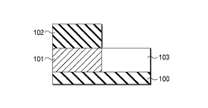
- FIG. 1A to 1F are sectional views showing an example of an etching method according to the first embodiment of the present invention.
- a barrier metal film 100 that prevents copper diffusion is formed on a semiconductor wafer (not shown), and a copper film 101 is formed on the barrier metal film 100.
- a mask material 102 is formed on the copper film 101.
- the mask material 102 has a role of blocking oxygen ions so that the oxygen ions do not reach the copper film 101. For this reason, the mask material 102 is required to have a large atomic weight and a large thickness. If possible, a material having an atomic weight larger than that of copper (Cu: atomic weight 63.546) and a high density is preferable.
- the film thickness of the mask material 102 is set such that oxygen ions do not reach the copper film 101. The film thickness of the mask material 102 can be reduced as the material has a higher atomic weight and higher density.
- the velocity energy (acceleration voltage) is set to the first value, and oxygen ions are irradiated toward the surface layer portion of the copper film 101.
- oxygen ions are irradiated toward the surface layer portion of the copper film 101.
- the velocity energy is set to a second value higher than the first value, and oxygen ions are irradiated toward the middle layer portion of the copper film 101.
- oxygen ions are irradiated toward the middle layer portion of the copper film 101.
- the velocity energy is set to a third value higher than the second value, and oxygen ions are irradiated toward the lower layer portion of the copper film 101.
- oxygen ions are irradiated toward the lower layer portion of the copper film 101.
- the copper film 101 is anisotropically oxidized, and the copper film 101 is changed into the copper oxide 103 in all the portions of the copper film 101 and the thickness direction of the copper film 101. The changed part is obtained.
- the velocity energy of oxygen necessary for oxidation can be obtained using a Monte Carlo simulator such as TRIM.
- the velocity energy of oxygen necessary for the oxidation is, for example, energy of 30 keV or more.
- Single oxygen molecular ions (O 2 + , O 2 2+ , O 2 ⁇ , O 2 2 ⁇ ) or oxygen ions (O + , O 2+ , O ⁇ , O 2 ⁇ ) separated by cracking have a velocity energy of 30 keV.
- oxygen ions are more preferable than oxygen molecular ions for oxidizing the lower layer portion of the copper film 101. It is advantageous.
- the velocity energy may be changed as in this example, or the molecular weight, that is, oxygen molecular ions or oxygen ions may be changed. That is, changing the implantation speed and implantation depth and sequentially oxidizing each of the surface layer portion, the middle layer portion, and the lower layer is effective in performing anisotropic oxidation of the copper film 101 in one process. .
- the semiconductor wafer having the structure shown in FIG. 1E is unloaded from the oxygen ion irradiation apparatus and loaded into an etching apparatus for etching the copper oxide 103.
- an etching apparatus for etching the copper oxide 103.
- both a wet etching apparatus and a dry etching apparatus can be used.
- wet etching apparatus examples include, as an etchant, a wet etching apparatus using an aqueous solution containing a citric acid containing a carboxyl group, an ascorbic acid, a malonic acid, and a malic acid. In such an aqueous solution, it is possible to dissolve only the copper oxide 103 without dissolving the copper film 101.
- the etchant may be an aqueous solution containing hydrofluoric acid. Hydrofluoric acid can also dissolve only the copper oxide 103 without dissolving the copper film 101.
- Hydrofluoric acid is also used for etching silicon oxide (SiO 2 ), and has an advantage that a high-purity chemical solution can be obtained.
- An example of a dry etching apparatus is a dry etching apparatus that etches and uses an organic compound gas.
- an organic compound gas that does not sublime the copper film 101 and sublimates only the copper oxide 103
- an organic acid gas such as a carboxylic acid having a carboxyl group (—COOH) can be given.
- carboxylic acid include carboxylic acids represented by the following formula (1).
- R 6 is hydrogen, or a linear or branched C 1 to C 20 alkyl group or alkenyl group, preferably methyl, ether, propyl, butyl, pentyl or hexyl
- R 6 is hydrogen, or a linear or branched C 1 to C 20 alkyl group or alkenyl group, preferably methyl, ether, propyl, butyl, pentyl or hexyl
- carboxylic acid represented by the formula (1) Formic acid (HCOOH) Acetic acid (CH 3 COOH) Propionic acid (CH 3 CH 2 COOH) Butyric acid (CH 3 (CH 2 ) 2 COOH) Valeric acid (CH 3 (CH 2 ) 3 COOH) Can be mentioned.
- organic compounds some organic acids are used in semiconductor processes, and high-purity chemicals can be obtained.
- copper can be etched anisotropically.
- the copper film 101 in the copper film 101, a portion that remains the copper film 101 and a portion that has changed to the copper oxide 103 in all the thickness directions of the copper film 101 are obtained.
- the copper film 101 is anisotropically oxidized in a single process. For this reason, the semiconductor wafer W does not need to be repeatedly transferred between the oxygen ion irradiation apparatus and the etching apparatus, and the throughput is high.
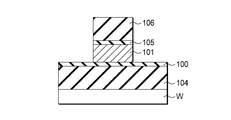
- (Second Embodiment) 2A to 2F are cross-sectional views showing an example of a semiconductor device manufacturing method according to the second embodiment of the present invention.
- a TEOS film 104 is formed on the semiconductor wafer W, and a SiCN film 100 is formed on the TEOS film 104.
- a copper film 101 is formed on the SiCN film 100, and a SiCN film 105 is formed on the copper film 101. Further, in this example, a TEOS film 106 is formed on the SiCN film 105.
- a photoresist film 107 is formed on the TEOS film 106 as a mask material.
- the TEOS film 106 and the SiCN film 105 are etched using the photoresist film 107 as a mask.
- the photoresist film 107 is removed.
- the copper film 101 is anisotropically etched by the etching method described in the first embodiment using the TEOS film 106 and the SiCN film 105 as a mask.
- the TEOS film 106 is removed.
- the SiCN film 105 is used as a barrier film on the upper surface of the copper film 101.
- the SiCN film 100 is used as a barrier film on the lower surface of the copper film 101.
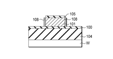
- an electroless plating method utilizing a selective precipitation phenomenon that has a catalytic action on the copper film 101 on the side surface of the copper film 101 and no catalytic action on the SiCN films 100 and 105.
- a plating film containing a substance that suppresses copper diffusion Is used to form a plating film containing a substance that suppresses copper diffusion.
- an alloy containing at least tungsten in cobalt, for example, a CoW film 108 is formed as the plating film.
- Such a second embodiment is effective for forming a copper wiring, and can be applied to, for example, a copper wiring forming process of a semiconductor integrated circuit device.
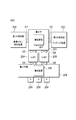
- FIG. 3 is a block diagram showing an example of an etching system according to the embodiment of the present invention.
- the etching system 200 includes a transfer chamber 201, a first processing chamber 202, a second processing chamber 203, a first load lock chamber (LLM1) 204, and a second load lock chamber (LLM2). 205 and a loading / unloading chamber 206.
- the transfer chamber 201 is connected to the first processing chamber 202, the second processing chamber 203, the first load lock chamber 204, and the second load lock chamber 205 via gate valves G1 to G4.
- a transfer device 207 is arranged in the transfer chamber 201. The transfer device 207 transfers the semiconductor wafer among the transfer chamber 201, the first processing chamber 202, the second processing chamber 203, the first load lock chamber 204, and the second load lock chamber 205.
- the first treatment chamber 202 is an oxygen ion irradiation device.
- the first processing chamber 202 is configured using, for example, an oxygen ion irradiation apparatus.
- the copper film 101 having the mask material 102 formed on the surface is irradiated with oxygen ions using the mask material as a mask, and all of the copper film 101 in the thickness direction of the copper film 101 is irradiated.
- copper oxide 103 that is anisotropically oxidized is formed.
- the second processing chamber 203 is an etching apparatus.
- the second treatment chamber 203 uses a wet etching apparatus using an aqueous solution containing an organic acid or an aqueous solution containing hydrofluoric acid, or a dry etching apparatus using a gas containing an organic compound, for example, an organic acid gas. Composed.
- the anisotropically oxidized copper oxide 103 is etched.
- the first load lock chamber 204 and the second load lock chamber 205 are pressure conversion devices. In the first load lock chamber 204 and the second load lock chamber 205, pressure conversion is performed between atmospheric pressure or almost atmospheric pressure and the pressure in the transfer chamber 201.
- the first load lock chamber 204 is connected to the carry-in / out chamber 206 through a gate valve G5.
- the second load lock chamber 205 is connected to the carry-in / out chamber 206 via a gate valve G6.
- the loading / unloading chamber 206 has a port (P) 208 on which a carrier containing a plurality of semiconductor wafers or an empty carrier is placed.
- P port
- a transfer device 209 is disposed in the carry-in / out chamber 206. The transfer device 209 transfers the semiconductor wafer among the carry-in / out chamber 206, the carrier placed in the port 208, the first load lock chamber 204, and the second load lock chamber 205.
- a first processing chamber 202 and a second processing chamber 203 are applied to a semiconductor wafer (object to be processed) including a copper film 101 and a mask material formed on the copper film 101.
- a semiconductor wafer object to be processed
- the etching method according to the first embodiment and the semiconductor device manufacturing method according to the second embodiment can be performed.
Landscapes
- Drying Of Semiconductors (AREA)
- Internal Circuitry In Semiconductor Integrated Circuit Devices (AREA)
- Weting (AREA)
Abstract
表面にマスク材(102)が形成された銅膜(101)に、マスク材(102)をマスクに用いて酸素イオン(6)を照射し、銅膜(101)内に、銅膜(101)の厚さ方向の全てに対して異方的に酸化された酸化銅(103)を形成する工程と、異方的に酸化された酸化銅(103)をエッチングする工程と、を具備する。
Description
この発明は、銅膜をエッチングするエッチング方法及びエッチングシステムに関する。
近時、半導体集積回路装置の動作の高速化が進展している。動作の高速化は、配線材料の低抵抗化などにより実現される。このため、配線材料は、従来のアルミニウムに代わり、より低抵抗な銅が用いられるようになってきている。
しかし、銅の加工には、既存のドライエッチング技術の転用が難しい。これは、エッチングの際に形成される銅の化合物は総じて蒸気圧が低く、蒸発し難いことに由来する。過去には、Arスパッタ法、ClガスRIE法などが試されたが、チャンバ内壁への銅の付着などの問題により実用化に至っていない。
このため、銅を用いた配線は、もっぱらダマシン法を用いて形成されている。ダマシン法は、あらかじめ配線パターンに応じた溝を層間絶縁膜に形成し、この溝を埋めるように銅薄膜を形成し、CMP法を用いて銅薄膜を化学的機械研磨し、溝の内部のみに銅を残す技術である。
銅を、塩化第二鉄水溶液を用いてウェットエッチングする、という技術もあるが、これは等方的なエッチングである。
一方、特許文献1には、銅の異方性ドライエッチング方法が記載されている。特許文献1の技術は、銅膜上にマスクを形成し、このマスクを介して銅膜に異方性酸化処理を施し、有機酸ガスにより酸化銅をエッチングするものである。
しかし、特許文献1では、銅膜の異方性酸化と、有機酸ガスによる酸化銅のエッチングとを繰り返す必要があるため、銅膜の異方性エッチングが終わるまで、異方性酸化装置と有機酸ドライエッチング装置との間で、銅膜が形成された半導体ウエハを動かし続けなければならない。このため、銅膜の異方性エッチングに時間がかかり、スループットが低いという問題がある。
この発明の目的は、高スループットで銅を異方的にエッチングすることが可能なエッチング方法及びエッチングシステムを提供することにある。
この発明の第1の観点によれば、表面にマスク材が形成された銅膜に、前記マスク材をマスクに用いて酸素イオンを照射し、前記銅膜内に、前記銅膜の厚さ方向の全てに対して異方的に酸化された酸化銅を形成する工程と、前記異方的に酸化された酸化銅をエッチングする工程と、を具備するエッチング方法が提供される。
この発明の第2の観点によれば、表面にマスク材が形成された銅膜に、前記マスク材をマスクに用いて酸素イオンを照射し、前記銅膜内に、前記銅膜の厚さ方向の全てに対して異方的に酸化された酸化銅を形成する酸素イオン照射装置と、前記異方的に酸化された酸化銅をエッチングするエッチング装置とを具備するエッチングシステムが提供される。
以下、この発明の実施形態を、図面を参照して説明する。なお、全図にわたり、共通の部分には共通の参照符号を付す。
(第1の実施形態)
半導体ウエハの断面例を参照しながら、この発明の第1の実施形態に係るエッチング方法について説明する。
半導体ウエハの断面例を参照しながら、この発明の第1の実施形態に係るエッチング方法について説明する。
図1A~図1Fはこの発明の第1の実施形態に係るエッチング方法の一例を示す断面図である。
図1Aに示すように、図示せぬ半導体ウエハ上には銅の拡散を防ぐバリアメタル膜100が形成されており、バリアメタル膜100上には銅膜101が形成されている。銅膜101上にはマスク材102が形成されている。
マスク材102は、酸素イオンが銅膜101に到達しないように、酸素イオンを遮断する役目を持つ。このため、マスク材102には、原子量が大きく、厚いことが求められる。可能であれば、銅(Cu:原子量63.546)よりも原子量が大きく、かつ、密度の高い材料が好ましい。マスク材102の膜厚は、酸素イオンが銅膜101に到達しないような厚さに設定される。マスク材102の膜厚は、原子量が大きく、かつ、密度の高い材料ほど、薄くすることが可能である。
次に、図1Bに示すように、速度エネルギー(加速電圧)を第1の値に設定し、酸素イオンを銅膜101の表層部分に向けて照射する。酸素イオンが銅膜101の表層部分に注入されることで、銅膜101の表層部分が酸化され、酸化銅103に変わる。
次に、図1Cに示すように、速度エネルギーを上記第1の値よりも高い第2の値に設定し、酸素イオンを銅膜101の中層部分に向けて照射する。酸素イオンが銅膜101の中層部分に注入されることで、銅膜101の中層部分が酸化され、酸化銅103に変わる。
次に、図1Dに示すように、速度エネルギーを上記第2の値よりも高い第3の値に設定し、酸素イオンを銅膜101の下層部分に向けて照射する。酸素イオンが銅膜101の下層部分に注入されることで、銅膜101の下層部分が酸化され、酸化銅103に変わる。
このようにして、速度エネルギーを高めながら酸素イオンを銅膜101に注入する。これにより、図1Eに示すように、銅膜101が異方的に酸化され、銅膜101には、銅膜101のままの部分と、銅膜101の厚さ方向の全てで酸化銅103に変化した部分とが得られる。
酸化に必要な酸素の速度エネルギーは、モンテカルロ・シミュレータ、例えば、TRIMを利用して求めることができる。酸化に必要な酸素の速度エネルギーは、例えば、30keV以上のエネルギーとなる。
単体の酸素分子イオン(O2
+、O2
2+、O2
-、O2
2-)、もしくはクラッキングにより乖離した酸素イオン(O+、O2+、O-、O2-)を、速度エネルギー30keV以上で加速し、銅膜101に照射することで、効率の良い酸化が可能となる。
また、分子量、原子量の低い酸化剤ほど、低い速度エネルギーで銅膜101の深い位置まで注入できるため、銅膜101の下層部分を酸化するためには、酸素分子イオンよりも、酸素イオンの方が有利である。
銅膜101全体を酸化する必要があることから、本例のように速度エネルギーを変化させたり、さらに、分子量、即ち、酸素分子イオンか酸素イオンかを変化させたりすることも良い。つまり、注入速度、注入深さを変化させ、表層部分、中層部分、下層のそれぞれを順次酸化させることが、1回のプロセスで銅膜101の異方性酸化を実行するうえで、有効である。
銅膜101の厚さ方向に対して全体が酸化されると、酸化銅103を除去することは容易であるため、繰り返しプロセスをする必要がなく、プロセス時間の短縮が可能であり、銅膜101の異方的なエッチングのスループットが高い。
次に、図1Eに示す構造を有した半導体ウエハを、酸素イオン照射装置から搬出し、酸化銅103をエッチングするエッチング装置に搬入する。このエッチング装置で、酸化銅103がエッチングされることで、図1Fに示すように、銅膜101の異方的なエッチングが終了する。
酸化銅103をエッチングするエッチング装置としては、ウェットエッチング装置、ドライエッチング装置の双方を使用することができる。
ウェットエッチング装置としては、エッチャントとして、カルボキシル基を含むクエン酸、同じくアスコルビン酸、同じくマロン酸、同じくリンゴ酸などの有機酸を含む水溶液を用いるウェットエッチング装置を挙げることができる。これらのような水溶液では、銅膜101を溶かさず、酸化銅103のみを溶かすことができる。
また、エッチャントとしては、弗化水素酸を含む水溶液でも良い。弗化水素酸も銅膜101を溶かさず、酸化銅103のみを溶かすことができる。
また、弗化水素酸は、シリコン酸化物(SiO2)のエッチングにも利用されており、高純度の薬液を入手できる、という利点もある。
また、ドライエッチング装置としては、エッチャントして、有機化合物ガスを用いるドライエッチング装置を挙げることができる。銅膜101は昇華させず、酸化銅103のみを昇華させる有機化合物ガスの例としては、有機酸ガス、例えば、カルボキシル基(-COOH)を有するカルボン酸を挙げることができる。カルボン酸の例としては、以下の式(1)で表されるカルボン酸を挙げることができる。
R6-COOH …(1)
(R6は水素、又は直鎖もしくは分枝鎖状のC1~C20のアルキル基もしくはアルケニル基、好ましくはメチル、エテル、プロピル、ブチル、ペンチル又はヘキシル)
式(1)で表されるカルボン酸の例としては、
蟻酸(HCOOH)
酢酸(CH3COOH)
プロピオン酸(CH3CH2COOH)
酪酸(CH3(CH2)2COOH)
吉草酸(CH3(CH2)3COOH)
を挙げることができる。
R6-COOH …(1)
(R6は水素、又は直鎖もしくは分枝鎖状のC1~C20のアルキル基もしくはアルケニル基、好ましくはメチル、エテル、プロピル、ブチル、ペンチル又はヘキシル)
式(1)で表されるカルボン酸の例としては、
蟻酸(HCOOH)
酢酸(CH3COOH)
プロピオン酸(CH3CH2COOH)
酪酸(CH3(CH2)2COOH)
吉草酸(CH3(CH2)3COOH)
を挙げることができる。
なお、有機化合物のうち、一部の有機酸は半導体プロセスで用いられており、高純度の薬液を入手することが可能である。
このような第1の実施形態によれば、銅を異方的にエッチングすることができる。
しかも、第1の実施形態によれば、銅膜101には、銅膜101のままの部分と、銅膜101の厚さ方向の全てで酸化銅103に変化した部分とが得られるように、1回のプロセスで銅膜101を異方的に酸化する。このため、半導体ウエハWは、酸素イオン照射装置とエッチング装置との間で繰り返し搬送する必要がなく、スループットが高い。
(第2の実施形態)
図2A~図2Fはこの発明の第2の実施形態に係る半導体装置の製造方法の一例を示す断面図である。
図2A~図2Fはこの発明の第2の実施形態に係る半導体装置の製造方法の一例を示す断面図である。
図2Aに示すように、半導体ウエハW上にはTEOS膜104が形成され、TEOS膜104上にはSiCN膜100が形成されている。SiCN膜100上には銅膜101が形成され、銅膜101上にはSiCN膜105が形成されている。さらに、本例ではSiCN膜105上にTEOS膜106が形成されている。
次に、図2Bに示すように、TEOS膜106上に、マスク材としてフォトレジスト膜107を形成する。
次に、図2Cに示すように、フォトレジスト膜107をマスクに用いて、TEOS膜106、およびSiCN膜105をエッチングする。
次に、図2Dに示すように、フォトレジスト膜107を除去する。次いで、TEOS膜106、およびSiCN膜105をマスクに用いて、上記第1の実施形態で説明したエッチング方法により、銅膜101を異方的にエッチングする。
次に、図2Eに示すように、TEOS膜106を除去する。SiCN膜105は、銅膜101の上面のバリア膜として使用される。また、SiCN膜100は、銅膜101の下面のバリア膜として使用される。
次に、図2Fに示すように、銅膜101の側面上に、銅膜101に対して触媒作用があり、SiCN膜100、105には触媒作用がない選択析出現象を利用した無電解めっき法を用いて、銅の拡散を抑制する物質を含むメッキ膜を形成する。本例ではメッキ膜として、コバルトに少なくともタングステンを含有させた合金、例えば、CoW膜108を形成する。
このような第2の実施形態は、銅配線の形成技術に有効であり、例えば、半導体集積回路装置の銅配線形成プロセスに適用することができる。
(エッチングシステム)
図3は、この発明の実施形態に係るエッチングシステムの一例を示すブロック図である。
図3は、この発明の実施形態に係るエッチングシステムの一例を示すブロック図である。
図3に示すように、エッチングシステム200は、搬送室201、第1の処理室202、第2の処理室203、第1のロードロック室(LLM1)204、第2のロードロック室(LLM2)205、及び搬入出室206を備えている。
搬送室201は、第1の処理室202、第2の処理室203、第1のロードロック室204、及び第2のロードロック室205に、ゲートバルブG1~G4を介して接続されている。搬送室201内には、搬送装置207が配置されている。搬送装置207は、搬送室201、第1の処理室202、第2の処理室203、第1のロードロック室204、及び第2のロードロック室205の相互間で半導体ウエハを搬送する。
第1の処理室202は、酸素イオン照射装置である。第1の処理室202は、例えば、酸素イオン照射装置を用いて構成される。第1の処理室202では、表面にマスク材102が形成された銅膜101に、マスク材をマスクに用いて酸素イオンを照射し、銅膜101内に、銅膜101の厚さ方向の全てに対して異方的に酸化された酸化銅103が形成される。
第2の処理室203は、エッチング装置である。第2の処理室203は、有機酸を含む水溶液、又は弗化水素酸を含む水溶液を用いたウェットエッチング装置、又は有機化合物を含むガス、例えば、有機酸ガスを用いたドライエッチング装置を用いて構成される。第2の処理室203では、上記異方的に酸化された酸化銅103がエッチングされる。
第1のロードロック室204及び第2のロードロック室205は、圧力変換装置である。第1のロードロック室204及び第2のロードロック室205では、大気圧もしくはほぼ大気圧と搬送室201内の圧力との間で、圧力変換が行われる。第1のロードロック室204は搬入出室206にゲートバルブG5を介して接続される。同じく第2のロードロック室205は搬入出室206にゲートバルブG6を介して接続される。
搬入出室206は、複数枚の半導体ウエハが収容されたキャリア、又は空のキャリアが載置されるポート(P)208を有する。キャリアがポート208に載置されると、図示せぬシャッタが外れ、キャリアの内部と搬入出室206の内部とが連通される。搬入出室206には搬送装置209が配置されている。搬送装置209は、搬入出室206、ポート208に載置されたキャリア、第1のロードロック室204、及び第2のロードロック室205の相互間で半導体ウエハを搬送する。
このようなエッチングシステムを用い、銅膜101と銅膜101上に形成されたマスク材とを備えた半導体ウエハ(被処理体)に対して、第1の処理室202、第2の処理室203の順で処理を進めることにより、上記第1の実施形態に係るエッチング方法、並びに上記第2の実施形態に係る半導体装置の製造方法を実施することができる。
以上、この発明を実施形態に従って説明したが、この発明は上記実施形態に限られるものではなく様々な変形が可能である。
101…銅膜、102…マスク材、103…酸化銅
Claims (8)
- 表面にマスク材が形成された銅膜に、前記マスク材をマスクに用いて酸素イオンを照射し、前記銅膜内に、前記銅膜の厚さ方向の全てに対して異方的に酸化された酸化銅を形成する工程と、
前記異方的に酸化された酸化銅をエッチングする工程と、
を具備するエッチング方法。 - 前記酸素イオンがO2以下の分子量のイオンを含む、請求項1に記載のエッチング方法。
- 前記酸化銅のエッチングは、有機酸を含む水溶液、又は弗化水素酸を含む水溶液を用いて行われる、請求項1に記載のエッチング方法。
- 前記有機酸を含む水溶液が、
カルボキシル基を含むクエン酸
カルボキシル基を含むアスコルビン酸
カルボキシル基を含むマロン酸
カルボキシル基を含むリンゴ酸
からなる群から選ばれたものである、請求項3に記載のエッチング方法。 - 前記酸化銅のエッチングは、有機化合物を含むガスを用いて行われる、請求項1に記載のエッチング方法。
- 前記有機化合物ガスが、カルボキシル基(-COOH)を有するカルボン酸である、請求項5に記載のエッチング方法。
- 前記有機化合物ガスとして用いられるカルボン酸は、下記(1)式で表されるものである、請求項6に記載のエッチング方法。
R3-COOH …(1)
(R3は水素、又は直鎖もしくは分枝鎖状のC1~C20のアルキル基もしくはアルケニル基) - 表面にマスク材が形成された銅膜に、前記マスク材をマスクに用いて酸素イオンを照射し、前記銅膜内に、前記銅膜の厚さ方向の全てに対して異方的に酸化された酸化銅を形成する酸素イオン照射装置と、
前記異方的に酸化された酸化銅をエッチングするエッチング装置と、
を具備する、エッチングシステム。
Applications Claiming Priority (2)
| Application Number | Priority Date | Filing Date | Title |
|---|---|---|---|
| JP2010193984A JP2012054305A (ja) | 2010-08-31 | 2010-08-31 | エッチング方法及びエッチングシステム |
| JP2010-193984 | 2010-08-31 |
Publications (1)
| Publication Number | Publication Date |
|---|---|
| WO2012029474A1 true WO2012029474A1 (ja) | 2012-03-08 |
Family
ID=45772583
Family Applications (1)
| Application Number | Title | Priority Date | Filing Date |
|---|---|---|---|
| PCT/JP2011/067399 Ceased WO2012029474A1 (ja) | 2010-08-31 | 2011-07-29 | エッチング方法及びエッチングシステム |
Country Status (3)
| Country | Link |
|---|---|
| JP (1) | JP2012054305A (ja) |
| TW (1) | TW201222730A (ja) |
| WO (1) | WO2012029474A1 (ja) |
Citations (7)
| Publication number | Priority date | Publication date | Assignee | Title |
|---|---|---|---|---|
| JPH02306631A (ja) * | 1989-05-22 | 1990-12-20 | Nec Corp | 半導体装置の銅配線形成方法 |
| JPH04324932A (ja) * | 1991-04-25 | 1992-11-13 | Nec Corp | Cu膜のエッチング方法 |
| JPH07302798A (ja) * | 1992-09-08 | 1995-11-14 | Intel Corp | 金属膜をエッチングする方法 |
| JPH0864606A (ja) * | 1994-08-22 | 1996-03-08 | Sharp Corp | 銅パターニング方法及びパターニング装置ならびに銅配線層を有する集積回路及びその製造方法 |
| JP2007086689A (ja) * | 2005-09-26 | 2007-04-05 | Kanto Chem Co Inc | フォトレジスト残渣及びポリマー残渣除去液 |
| JP2009043976A (ja) * | 2007-08-09 | 2009-02-26 | Tokyo Electron Ltd | 銅の再付着防止方法、半導体装置の製造方法、基板処理装置及び記憶媒体 |
| JP2009218276A (ja) * | 2008-03-07 | 2009-09-24 | Tokyo Electron Ltd | ドライクリーニング方法および基板処理装置 |
-
2010
- 2010-08-31 JP JP2010193984A patent/JP2012054305A/ja active Pending
-
2011
- 2011-07-29 WO PCT/JP2011/067399 patent/WO2012029474A1/ja not_active Ceased
- 2011-08-30 TW TW100131122A patent/TW201222730A/zh unknown
Patent Citations (7)
| Publication number | Priority date | Publication date | Assignee | Title |
|---|---|---|---|---|
| JPH02306631A (ja) * | 1989-05-22 | 1990-12-20 | Nec Corp | 半導体装置の銅配線形成方法 |
| JPH04324932A (ja) * | 1991-04-25 | 1992-11-13 | Nec Corp | Cu膜のエッチング方法 |
| JPH07302798A (ja) * | 1992-09-08 | 1995-11-14 | Intel Corp | 金属膜をエッチングする方法 |
| JPH0864606A (ja) * | 1994-08-22 | 1996-03-08 | Sharp Corp | 銅パターニング方法及びパターニング装置ならびに銅配線層を有する集積回路及びその製造方法 |
| JP2007086689A (ja) * | 2005-09-26 | 2007-04-05 | Kanto Chem Co Inc | フォトレジスト残渣及びポリマー残渣除去液 |
| JP2009043976A (ja) * | 2007-08-09 | 2009-02-26 | Tokyo Electron Ltd | 銅の再付着防止方法、半導体装置の製造方法、基板処理装置及び記憶媒体 |
| JP2009218276A (ja) * | 2008-03-07 | 2009-09-24 | Tokyo Electron Ltd | ドライクリーニング方法および基板処理装置 |
Also Published As
| Publication number | Publication date |
|---|---|
| JP2012054305A (ja) | 2012-03-15 |
| TW201222730A (en) | 2012-06-01 |
Similar Documents
| Publication | Publication Date | Title |
|---|---|---|
| JP6921990B2 (ja) | 超伝導体相互接続のための予洗浄および堆積の方法 | |
| US8080475B2 (en) | Removal chemistry for selectively etching metal hard mask | |
| KR101082993B1 (ko) | 레지스트용 박리제조성물 및 반도체장치의 제조방법 | |
| AU2017345050B2 (en) | Preclean methodology for superconductor interconnect fabrication | |
| JP7507761B2 (ja) | 金属層をパターニングする方法 | |
| KR102584970B1 (ko) | 금속들의 원자 층 에칭 | |
| TW200952117A (en) | Semiconductor interconnect air gap formation process | |
| WO2015153040A1 (en) | Integrated metal spacer and air gap interconnect | |
| JPH05291208A (ja) | ドライエッチング方法 | |
| JP2012119686A (ja) | 金属含有犠牲材料及びダマシン配線形成の方法 | |
| JPH0950986A (ja) | 接続孔の形成方法 | |
| KR100834396B1 (ko) | 반도체 소자의 패턴 형성 방법 | |
| JP5476161B2 (ja) | 半導体装置の製造方法 | |
| US7037822B2 (en) | Method of forming metal line in semiconductor device | |
| US20190198325A1 (en) | Extreme ultraviolet (euv) lithography patterning methods utilizing euv resist hardening | |
| JP2007300125A (ja) | 半導体素子の微細パターンの形成方法 | |
| US12051619B2 (en) | Semiconductor device and method of manufacture | |
| JP2009076615A (ja) | 半導体装置の製造方法 | |
| US6875702B2 (en) | Plasma treatment system | |
| KR20130092570A (ko) | 반도체 장치의 제조 방법 | |
| WO2012029474A1 (ja) | エッチング方法及びエッチングシステム | |
| JP2012114287A (ja) | パターン化金属膜及びその形成方法 | |
| JP2001284355A (ja) | 半導体装置およびその製造方法 | |
| JP2005303191A (ja) | 半導体装置の製造方法 | |
| JP2012054306A (ja) | 半導体装置の製造方法 |
Legal Events
| Date | Code | Title | Description |
|---|---|---|---|
| 121 | Ep: the epo has been informed by wipo that ep was designated in this application |
Ref document number: 11821492 Country of ref document: EP Kind code of ref document: A1 |
|
| NENP | Non-entry into the national phase |
Ref country code: DE |
|
| 122 | Ep: pct application non-entry in european phase |
Ref document number: 11821492 Country of ref document: EP Kind code of ref document: A1 |