WO2012023271A1 - 撮像装置 - Google Patents
撮像装置 Download PDFInfo
- Publication number
- WO2012023271A1 WO2012023271A1 PCT/JP2011/004560 JP2011004560W WO2012023271A1 WO 2012023271 A1 WO2012023271 A1 WO 2012023271A1 JP 2011004560 W JP2011004560 W JP 2011004560W WO 2012023271 A1 WO2012023271 A1 WO 2012023271A1
- Authority
- WO
- WIPO (PCT)
- Prior art keywords
- signal
- unit
- horizontal
- period
- sampling
- Prior art date
- Legal status (The legal status is an assumption and is not a legal conclusion. Google has not performed a legal analysis and makes no representation as to the accuracy of the status listed.)
- Ceased
Links
Images



Classifications
-
- H—ELECTRICITY
- H10—SEMICONDUCTOR DEVICES; ELECTRIC SOLID-STATE DEVICES NOT OTHERWISE PROVIDED FOR
- H10F—INORGANIC SEMICONDUCTOR DEVICES SENSITIVE TO INFRARED RADIATION, LIGHT, ELECTROMAGNETIC RADIATION OF SHORTER WAVELENGTH OR CORPUSCULAR RADIATION
- H10F39/00—Integrated devices, or assemblies of multiple devices, comprising at least one element covered by group H10F30/00, e.g. radiation detectors comprising photodiode arrays
- H10F39/80—Constructional details of image sensors
- H10F39/803—Pixels having integrated switching, control, storage or amplification elements
-
- H—ELECTRICITY
- H04—ELECTRIC COMMUNICATION TECHNIQUE
- H04N—PICTORIAL COMMUNICATION, e.g. TELEVISION
- H04N25/00—Circuitry of solid-state image sensors [SSIS]; Control thereof
- H04N25/60—Noise processing, e.g. detecting, correcting, reducing or removing noise
- H04N25/62—Detection or reduction of noise due to excess charges produced by the exposure, e.g. smear, blooming, ghost image, crosstalk or leakage between pixels
- H04N25/626—Reduction of noise due to residual charges remaining after image readout, e.g. to remove ghost images or afterimages
-
- H—ELECTRICITY
- H04—ELECTRIC COMMUNICATION TECHNIQUE
- H04N—PICTORIAL COMMUNICATION, e.g. TELEVISION
- H04N25/00—Circuitry of solid-state image sensors [SSIS]; Control thereof
- H04N25/60—Noise processing, e.g. detecting, correcting, reducing or removing noise
- H04N25/67—Noise processing, e.g. detecting, correcting, reducing or removing noise applied to fixed-pattern noise, e.g. non-uniformity of response
-
- H—ELECTRICITY
- H04—ELECTRIC COMMUNICATION TECHNIQUE
- H04N—PICTORIAL COMMUNICATION, e.g. TELEVISION
- H04N25/00—Circuitry of solid-state image sensors [SSIS]; Control thereof
- H04N25/70—SSIS architectures; Circuits associated therewith
- H04N25/76—Addressed sensors, e.g. MOS or CMOS sensors
- H04N25/7795—Circuitry for generating timing or clock signals
Definitions
- the present invention relates to an imaging apparatus.
- a plurality of pixels arranged two-dimensionally includes a photoelectric conversion unit, a charge-voltage conversion unit that converts charges transferred from the photoelectric conversion unit, to the voltage, A transfer unit that transfers charges from the photoelectric conversion unit to the charge-voltage conversion unit, an amplification unit that outputs a signal corresponding to the voltage of the charge-voltage conversion unit, and a reset unit that resets the voltage of the charge-voltage conversion unit, respectively Have.
- a plurality of types of drive signals for example, binary signals that turn on and off the transfer unit, reset
- This vertical scanning circuit is generally an output of a shift register and other digital circuits, and a buffer circuit or the like that converts signals obtained by these circuits into signals having necessary driving ability and outputs the signals as the driving signals. And a circuit.
- a vertical signal line provided corresponding to each column of a plurality of pixels, to which an output signal of a pixel in the corresponding column is supplied, and a signal corresponding to the signal of each vertical signal line
- a sample hold unit that samples and holds a signal according to a sampling control signal and supplies the held signal to a horizontal signal line according to a horizontal scan signal
- a horizontal scan unit that supplies the horizontal scan signal to the sample hold unit It is equipped with.
- a horizontal unit that supplies a plurality of types of pulse signals related to reading of signals from the sample-and-hold unit to the horizontal signal line as a control unit that controls the solid-state imaging device.
- a control unit having a drive control unit is used.
- the present invention has been made in view of such circumstances, and an object thereof is to provide an imaging apparatus capable of reducing an afterimage phenomenon.
- An imaging apparatus includes a photoelectric conversion unit, a charge-voltage conversion unit that converts charges transferred from the photoelectric conversion unit into a voltage, a transfer unit that transfers charges from the photoelectric conversion unit to the charge-voltage conversion unit,
- Each of the amplifying unit that outputs a pixel signal corresponding to the voltage of the charge-voltage conversion unit and the reset unit that resets the voltage of the charge-voltage conversion unit has a plurality of pixels arranged two-dimensionally, and
- a vertical drive unit that supplies a drive signal for driving the pixel to a plurality of pixels, a vertical signal line that is provided corresponding to each column of the plurality of pixels, and that supplies the pixel signal, and the vertical
- a sample hold unit that samples and holds the pixel signal supplied to the signal line according to a sampling control signal and supplies the pixel signal to the horizontal signal line according to a horizontal drive signal; and the sample hold unit A horizontal drive unit that supplies the horizontal drive signal; and a horizontal drive control
- a circuit that controls the reset unit among the vertical driving units is operated by the same power source as the horizontal driving unit.
- the horizontal drive control unit supplies the plurality of types of pulse signals to the horizontal drive unit in each horizontal readout period.
- the horizontal drive control unit includes at least a part of a period from a start time of each horizontal blanking period to a last signal sampling time in the horizontal blanking period among signal sampling times determined by the sampling control signal.
- the dummy pulse signal is supplied to the horizontal drive unit.
- the dummy pulse signal is the same signal as one or more of the plurality of types of pulse signals.
- the one or more types of pulse signals are supplied to the horizontal driving unit, and the horizontal driving unit causes the horizontal driving signal to be generated. It includes a pulse signal.
- the horizontal driving unit includes a shift register unit, and the at least one pulse signal includes a driving clock signal for driving the shift register unit.
- the horizontal drive control unit stops the dummy pulse signal at the signal sampling time point.
- the signal sampling point in each horizontal blanking period samples an optical signal including optical information photoelectrically converted by the pixel. And a first sampling time point for sampling a differential signal including a noise component to be subtracted from the optical signal, and immediately before the first sampling time point in each horizontal blanking period.
- the vertical drive unit performs the horizontal sampling from the last signal sampling time in the horizontal blanking period in each horizontal blanking period.
- a drive signal for controlling the reset unit is supplied to the reset unit so as to cause the reset unit to perform a reset operation in at least a part of a period until the end of the blanking period. .
- An imaging device includes a photoelectric conversion unit, a charge-voltage conversion unit that converts charge transferred from the photoelectric conversion unit into a voltage, a transfer unit that transfers charge from the photoelectric conversion unit to the charge-voltage conversion unit,
- Each of the amplifying unit that outputs a pixel signal corresponding to the voltage of the charge-voltage conversion unit and the reset unit that resets the voltage of the charge-voltage conversion unit has a plurality of pixels arranged two-dimensionally, and
- a vertical drive unit that supplies a drive signal for driving the pixel to a plurality of pixels, a vertical signal line that is provided corresponding to each column of the plurality of pixels, and that supplies the pixel signal, and the vertical
- a sample hold unit that samples and holds the pixel signal according to the signal of the signal line according to the sampling control signal, and supplies the held signal to the horizontal signal line according to the horizontal drive signal; It is those with a.
- the vertical driving unit includes at least a part of a period from the last signal sampling time point to the end time point of the horizontal blanking period in each horizontal blanking period. In this period, a drive signal for controlling the reset unit is supplied to the reset unit so that the reset unit performs a reset operation.
- An image pickup apparatus is related to the eighth aspect according to the eighth aspect, wherein the horizontal drive unit supplies the horizontal drive signal to the sample hold unit, and the signal is read from the sample hold unit to the horizontal signal line. And a horizontal drive control unit that supplies a plurality of types of pulse signals.
- a circuit that controls the reset unit is operated by the same power source as the horizontal driving unit.
- the plurality of pixels are arranged for each of a predetermined number of two or more pixels in which the photoelectric conversion units are sequentially arranged in a column direction.
- the charge voltage conversion unit, the amplification unit, and the reset unit are shared.
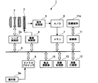
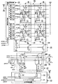
- FIG. 1 is a schematic block diagram illustrating an imaging apparatus according to a first embodiment of the present invention. It is a circuit diagram which shows schematic structure of the solid-state image sensor in FIG.
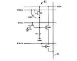
- FIG. 2 is a circuit diagram illustrating parasitic capacitance and the like of one pixel in FIG. 1.
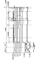
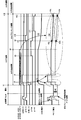
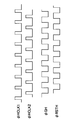
- 3 is a timing chart illustrating an operation of the imaging apparatus according to the first embodiment of the present invention. It is a timing chart which shows operation of an imaging device by a comparative example.
- 5 is a timing chart showing a part of the timing chart shown in FIG. It is a figure which shows typically the relationship between the electric potential of a floating capacitance part, and the electric potential of a vertical signal line.
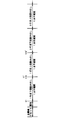
- FIG. 9 It is a circuit diagram which shows schematic structure of the solid-state image sensor of the imaging device by the 2nd Embodiment of this invention. It is a figure which shows each operation
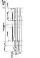
- 10 is a timing chart showing an all-pixel reset period, an exposure period, and a readout period of pixels on the lower side of the pixel block in the first row in FIG. 9.
- 10 is a timing chart illustrating a readout period of pixels on the upper side of the pixel block in the first row in FIG. 9.
- FIG. 1 is a schematic block diagram showing an imaging apparatus 1 according to the first embodiment of the present invention.
- the imaging device 1 according to the present embodiment is configured as an electronic camera.
- FIG. 1 shows that an imaging lens 2 is attached to an imaging apparatus 1 according to the present embodiment.
- the photographing lens 2 is driven by a lens control unit 2a for focus and diaphragm.
- the imaging surface of the solid-state imaging device 3 is arranged.
- the solid-state imaging device 3 is driven by a control signal output from the imaging control unit 4 and outputs a signal.
- a signal output from the solid-state imaging device 3 is processed through the signal processing unit 5 and the A / D conversion unit 6 and then temporarily stored in the memory 7.
- the memory 7 is connected to the bus 8.
- the bus 8 is also connected with a lens control unit 2a, an imaging control unit 4, a microprocessor 9, a focus calculation unit 10, a recording unit 11, an image compression unit 12, an image processing unit 13, and the like.
- An operation unit 9 a such as a release button is connected to the microprocessor 9.
- a recording medium 11a is detachably attached to the recording unit 11 described above.
- the imaging control unit 4 is composed of a timing generator or the like, and a control signal described later to the vertical scanning circuit 22 (see FIG. 2) and the horizontal scanning circuit 23 (see FIG. 2) of the solid-state imaging device 3.
- ⁇ GH, ⁇ HCLK1, ⁇ HCLK2, ⁇ HSTR, ⁇ RSTH, ⁇ VCLK1, ⁇ VCLK2, ⁇ VSTR, ⁇ TVS, ⁇ TVN, and the like are supplied to control the solid-state imaging device 3.
- FIG. 2 is a circuit diagram showing a schematic configuration of the solid-state imaging device 3 in FIG.
- the solid-state imaging device 3 has a plurality of two-dimensionally arranged pixels 21 (in FIG. 1, only 2 ⁇ 2 pixels 21 are shown) as in a general CMOS solid-state imaging device. ), A vertical scanning circuit (vertical driving unit) 22, a horizontal scanning circuit (horizontal driving unit) 23, and an output signal (pixel signal) of a pixel 21 in a corresponding column provided corresponding to each column of pixels 21. are provided, and a constant current source 25 connected to each vertical signal line 24. Needless to say, the number of pixels 21 is not limited.
- a floating capacitance unit FD as a charge-voltage conversion unit, a transfer transistor TX as a charge transfer unit that transfers charges from the photodiode PD to the floating capacitance unit FD, and a pixel signal corresponding to the voltage of the floating capacitance unit FD 2 includes an amplification transistor AMP as an amplification unit, a reset transistor RES as a reset unit that resets the voltage of the floating capacitance unit FD, and a selection transistor SEL as a selection unit for selecting the pixel 21.
- the transistors AMP, TX, RES, and SEL of the pixel 21 are all nMOS transistors. Each pixel 21 is operated by a first power source, and each amplification transistor AMP is also operated by the first power source.
- AVDD is the power supply potential of the first power supply
- AGND is the ground potential of the first power supply.
- FIG. 3 is a circuit diagram showing the parasitic capacitance CRES and the like of one pixel 21 in FIG.
- the gate of the transfer transistor TX is connected to a drive signal line that guides the transfer drive signal ⁇ TX from the vertical scanning circuit 22 for each pixel row.
- the gate of the reset transistor RES is connected to a drive signal line that guides the drive signal ⁇ RES from the vertical scanning circuit 22 for each pixel row.
- the gate of the selection transistor SEL is connected to a drive signal line that guides the drive signal ⁇ SEL from the vertical scanning circuit 22 for each pixel row.
- the photodiode PD generates a signal charge according to the amount of incident light (subject light).
- the transfer transistor TX is turned on during a high level period of the transfer pulse (driving signal) ⁇ TX, and transfers the signal charge accumulated in the photodiode PD to the floating capacitor FD.
- the reset transistor RES is turned on during the high level period of the reset pulse (drive signal) ⁇ RES, and resets the floating capacitor FD.
- the amplification transistor AMP has a drain connected to the power supply potential AVDD of the first power supply, a gate connected to the floating capacitor FD, a source connected to the drain of the selection transistor SEL, and a constant current source 25.
- a source follower circuit having a transistor TD provided corresponding to each vertical signal line 24 as a load is configured.
- the drain of each transistor TD is connected to each vertical signal line 24, and the source of each transistor TD is connected to the ground potential AGND of the first power supply.
- the gates of the transistors TD are commonly connected to a constant current setting circuit obtained by a constant current setting circuit including a resistor RL and a transistor TS connected between the power supply potential AVDD and the ground potential AGND of the first power supply. A voltage is given.
- the constant current source 25 causes a current to flow through the vertical signal line 24 when the selection transistor SEL of the pixel 21 corresponding to the vertical signal line 24 is turned on.
- This current is a source follower bias current of the amplification transistor AMP of the pixel 21.
- the amplification transistor AMP outputs a voltage to the vertical signal line 24 via the selection transistor SEL in accordance with the voltage value of the floating capacitor FD.
- the selection transistor SEL is turned on during a high level period of the selection pulse (drive signal) ⁇ SEL, and connects the source of the amplification transistor AMP to the vertical signal line 24.
- the vertical scanning circuit 22 receives the two-phase vertical drive clock signals ⁇ VCLK1 and ⁇ VCLK2 and the vertical start pulse signal ⁇ VSTR as vertical drive control signals each composed of a pulse signal from the imaging control unit 4, and for each row of the pixels 21.
- the selection pulse ⁇ SEL, the reset pulse ⁇ RES, and the transfer pulse ⁇ TX are output.
- n indicates a signal of the pixel in the nth row.
- the vertical scanning circuit 22 includes a signal generation circuit 30 and buffer circuits B1 to B3.
- the signal generation circuit 30 includes a shift register and other digital circuits, and receives the vertical drive control signal from the imaging control unit 4 to generate a selection pulse ⁇ SEL, a reset pulse ⁇ RES, and a transfer pulse ⁇ TX for each pixel row. Each corresponding signal is generated. Therefore, the signal generation circuit 30 includes all digital circuits other than the buffer circuits B1 to B3 in the vertical scanning circuit 22.
- the buffer circuits B1 to B3 are provided for each pixel row. Each buffer circuit B1 converts a signal from the signal generation circuit 30 corresponding to the reset pulse ⁇ RES into a reset pulse ⁇ RES having necessary driving capability for each pixel row corresponding to the pixel row, and outputs this.
- Each buffer circuit B2 converts a signal from the signal generation circuit 30 corresponding to the transfer pulse ⁇ TX into a transfer pulse ⁇ TX having a necessary drive capability and the like for each corresponding to each pixel row, and outputs this.
- Each buffer circuit B3 converts a signal from the signal generation circuit 30 corresponding to the selection pulse ⁇ SEL into a selection pulse ⁇ SEL having a necessary driving capability for each pixel row corresponding to each pixel row, and outputs this.
- the buffer circuits B1 to B3 constitute a drive output circuit that outputs three types of drive signals ⁇ RES, ⁇ TX, and ⁇ SEL that drive the pixel 21.
- the signal generation circuit 30 and the buffer circuits B1 to B3 of the vertical scanning circuit 22 are operated by a second power source of a different system different from the first power source (the ground potential AGND and the power source potential AVDD). It is like that.
- DVDD is the power supply potential of the second power supply
- DGND is the ground potential of the second power supply.
- the horizontal scanning circuit 23 receives horizontal drive control signals ⁇ GH, ⁇ HCLK1, ⁇ HCLK2, and ⁇ HSTR, each of which is a pulse signal from the imaging control unit 4, and outputs a horizontal scan signal (horizontal drive signal) ⁇ H for each column.
- m indicates a signal of a pixel in the m-th column.
- the horizontal scanning circuit 23 is provided for each column, with a shift register unit 31 driven by receiving the two-phase horizontal drive clock signals ⁇ HCLK1 and ⁇ HCLK2 and the horizontal start pulse signal ⁇ HSTR from the imaging control unit 4.
- a gate unit 33 that generates the horizontal scanning signal ⁇ H by gating the output signal of each stage of the shift register unit 31 according to the gate control signal ⁇ GH from the imaging control unit 4. ing.
- One input terminal of each AND gate 32 is connected in common, and a gate control signal ⁇ GH is input thereto.
- the output signal of each stage of the shift register unit 31 is input to the other input terminal of each AND gate 32.
- the gate control signal ⁇ GH is a pulse signal for setting the pulse width of the horizontal scanning signal ⁇ H.
- the horizontal scanning signal ⁇ H for each column is output from the output terminal of each AND gate 32.
- the horizontal drive control signals ⁇ GH, ⁇ HCLK1, ⁇ HCLK2, and ⁇ HSTR are pulse signals that are supplied to the horizontal scanning circuit 23 and cause the horizontal scanning circuit 23 to generate the horizontal scanning signal ⁇ H.
- the horizontal scanning circuit 23 is operated by the second power supply (the ground potential DGND and the power supply potential DVDD) in the same manner as the vertical scanning circuit 22.
- the solid-state imaging device 3 samples and holds signals according to the signals of the vertical signal lines 24 according to the sampling control signals ⁇ TVN and ⁇ TVS, and also holds the held signals according to the horizontal scanning signal ⁇ H. , 26S, a sample hold unit 27 is provided.
- the sample hold unit 27 includes optical signal storage capacitors CS and dark signal storage capacitors CN provided corresponding to the respective vertical signal lines 24, and optical information photoelectrically converted by the pixels 21.
- An optical signal sampling switch TVS for storing the optical signal in the optical signal storage capacitor CS in accordance with the optical signal sampling control signal ⁇ TVS, and a so-called dark signal as a differential signal including a noise component to be subtracted from the optical signal is a dark signal.
- the dark signal sampling switch TVN for storing in the dark signal storage capacitor CN in accordance with the sampling control signal ⁇ TVN and the optical signal stored in the optical signal storage capacitor CS are supplied to the optical signal horizontal signal line 26S in accordance with the horizontal scanning signal ⁇ H.
- Output amplifiers APS and APN are connected to the horizontal signal lines 26S and 26N, respectively.
- the switches TVS, TVN, THS, and THN are all nMOS transistors.
- the gates of the optical signal sampling switches TVS are connected in common, and an optical signal sampling control signal ⁇ TVS is supplied from the imaging control unit 4 to the gate.
- an optical signal sampling control signal ⁇ TVS is supplied from the imaging control unit 4 to the gate.
- the optical signal sampling switch TVS is turned on in response to the optical signal sampling control signal ⁇ TVS, the optical signal on the vertical signal line 24 is stored in the corresponding optical signal storage capacitor CS.
- the level of the optical signal stored in the optical signal storage capacitor CS is determined by the level of the signal on the vertical signal line 24 when the optical signal sampling switch TVS is turned off (that is, when ⁇ TVS falls). The That is, the falling time of the optical signal sampling control signal ⁇ TVS is the optical signal sampling time.
- the gates of the dark signal sampling switches TVN are connected in common, and a dark signal sampling control signal ⁇ TVN is supplied from the imaging control unit 4 thereto.
- a dark signal sampling control signal ⁇ TVN is supplied from the imaging control unit 4 thereto.
- the dark signal sampling switch TVN is turned on in response to the dark signal sampling control signal ⁇ TVN, the dark signal on the vertical signal line 24 is stored in the corresponding dark signal storage capacitor CN.
- the level of the dark signal stored in the dark signal storage capacitor CN is determined by the level of the signal on the vertical signal line 24 at the time when the dark signal sampling switch TVN is turned off (that is, when ⁇ TVN falls). The That is, the falling time of the dark signal sampling control signal ⁇ TVN is the dark signal sampling time.
- the gates of the optical signal horizontal transfer switch THS and the dark signal horizontal transfer switch THN are connected in common to each column, and the horizontal scanning signal ⁇ H of the corresponding column is supplied from the horizontal scanning circuit 23 to the gate.
- the horizontal transfer switches THS and THN of each column are turned on in accordance with the horizontal scanning signal ⁇ H of each column, the optical signal stored in the optical signal storage capacitor CS and the dark signal storage capacitor CN of the corresponding column and
- the dark signals are respectively output to the optical signal horizontal signal line 26S and the dark signal horizontal signal line 26N, and are output to the signal processing unit 5 in FIG. 1 through the output amplifiers APS and APN, respectively.
- the output amplifiers APS and APN are operated by the first power supply (ground potential AGND and power supply potential AVDD).
- the solid-state imaging device 3 includes horizontal line reset transistors RSTS and RSTN for resetting the horizontal signal lines 26S and 26N to a predetermined potential VREF in accordance with the horizontal line reset control signal ⁇ RSTH.
- the horizontal line reset transistors RSTS and RSTN are all nMOS transistors. The gates of the horizontal line reset transistors RSTS and RSTN are connected in common, and a horizontal line reset control signal ⁇ RSTH is supplied from the imaging control unit 4 thereto.
- the horizontal line reset transistors RSTS and RSTN are turned on in response to the horizontal line reset control signal ⁇ RSTH, the horizontal signal lines 26S and 26N are reset to the predetermined potential VREF, respectively.
- the horizontal line reset control signal ⁇ RSTH is a pulse signal related to reading of signals from the sample hold unit 27 to the horizontal signal lines 26S and 26N.
- the signal processing unit 5 obtains the difference between the outputs of the output amplifiers APS and APN using a differential amplifier or the like.
- a differential amplifier or the like that obtains such a difference may be mounted on the solid-state imaging device 3.
- the imaging control unit 4 has a function of supplying pulse signals ⁇ GH, ⁇ HCLK1, ⁇ HCLK2, ⁇ HSTR, and ⁇ RSTH related to reading of signals from the sample hold unit 27 to the horizontal signal lines 26S and 26N.
- the horizontal drive control unit is configured.
- the horizontal drive control unit (that is, the imaging control unit 4) starts from the start time of each horizontal blanking period, during the signal sampling time determined by the sampling control signals ⁇ TVN and ⁇ TVS, in the horizontal blanking period.
- one or more kinds of pulse signals ⁇ GH, ⁇ HCLK1, among a plurality of types of pulse signals ⁇ GH, ⁇ HCLK1, ⁇ HCLK2, ⁇ HSTR, ⁇ RSTH are used as dummy pulse signals.
- the same signals as ⁇ HCLK 2 and ⁇ RSTH are supplied to the horizontal scanning circuit 23. This point will be described in detail later with reference to FIG.
- the same symbols ⁇ GH, ⁇ HCLK1, ⁇ HCLK2, and ⁇ RSTH are also given to the dummy pulse signals corresponding to the pulse signals ⁇ GH, ⁇ HCLK1, ⁇ HCLK2, and ⁇ RSTH, respectively.
- the portion within the horizontal scanning period is the original pulse signal (pulse signal related to the readout of signals from the sample hold unit 27 to the horizontal signal lines 26S and 26N).
- the portion in the horizontal blanking period is a dummy pulse signal.
- FIG. 4 is a timing chart showing an example of the reading operation of the imaging apparatus 1 according to the present embodiment.
- a period indicated by a square with an x inside indicates a period in which the control signals ⁇ GH, ⁇ HCLK1, ⁇ HCLK2, and ⁇ RSTH are repeatedly generated as pulse signals at a high frequency.
- these control signals ⁇ GH, ⁇ HCLK1, ⁇ HCLK2, and ⁇ RSTH have the same waveform as that shown in FIG. 6 when a part of the period is enlarged.
- these control signals ⁇ GH, ⁇ HCLK1, ⁇ HCLK2, and ⁇ RSTH have the same frequency, but the pulse width and phase are set as shown in FIG.
- the horizontal start pulse signal ⁇ HSTR has a low level in a steady state, and is a high level one pulse only at the start of each horizontal scanning period described later.
- periods other than the period indicated by a square marked with “x” are not explicitly shown in the drawing, but the control signals ⁇ GH, ⁇ HCLK1, ⁇ HCLK2, and ⁇ RSTH are stopped and set to the high level or the low level, respectively. It is fixed.
- FIG. 4 mainly shows an operation in the case where the all pixel reset period, the exposure period, and one horizontal period related to the pixels 21 in the first row are performed, and subsequently, one horizontal period related to the pixels 21 in the second row is performed. .
- the all-pixel reset period all rows of reset pulses ⁇ RES are once set to high level, and ⁇ TX of all rows are once set to high level at the same time.
- FIG. 5 is a timing chart showing the reading operation of the imaging apparatus according to the comparative example compared with the imaging apparatus 1 according to the present embodiment.
- the same reference numerals are assigned to the signals that are the same as or correspond to the signals in FIG. 4.
- the only difference between the image pickup apparatus according to this comparative example and the image pickup apparatus 1 according to this embodiment is the control of the image pickup control unit 4 and the control of the vertical scanning circuit 22.
- dummy pulse signals ⁇ GH, ⁇ HCLK1, ⁇ HCLK2, and ⁇ RSTH are supplied during the period t9-t12 in the horizontal blanking period of the horizontal period of the first row ([5 in FIG. 4]
- the same applies to other horizontal periods.
- the pulse signals [phi] GH, [phi] HCLK1, [phi] HCLK2, and [phi] RSTH are stopped and the same applies to other horizontal periods.
- the reset pulse ⁇ RES (1) is set to the high level during the period t14-t15 in the horizontal blanking period of the first row (see [6] in FIG. 4).
- the reset pulse ⁇ RES (1) is also applied during the period t14-t15 in the horizontal blanking period of the first row as shown in FIG. This is the same for the other horizontal periods.
- the present embodiment and the comparative example differ in the ground potential DGND of the second power source and the potential of the reset pulse ⁇ RES as shown in FIGS. As can be understood from FIGS. 2 and 3, the low level of the reset pulse ⁇ RES is supplied from the ground potential DGND.
- the period t1-t16 is one horizontal period related to the pixels 21 in the first row.
- the period t1-t6 is a horizontal scanning period (horizontal readout period)
- the period t6-t16 is a horizontal blanking period.
- high-frequency pulse signals ⁇ GH, ⁇ HCLK1, ⁇ HCLK2, and ⁇ RSTH are supplied during the horizontal scanning period t1-t6, while pulse signals ⁇ GH, ⁇ HCLK1, ⁇ HCLK2, and ⁇ RSTH are supplied during the horizontal blanking period t6-t16. Stopped.
- the reset pulse ⁇ RES (1) is set to the high level and the reset transistor RES is turned on.
- the reset pulse ⁇ RES (1) is set to the low level, and the reset transistors RES in the first row are turned off.
- the selection pulse ⁇ SEL (1) is set to the high level and the selection transistors in the first row are turned on.
- the selection transistor SEL in the first row is turned on and the reset transistor RES in the first row is turned off at the same time, so that the gate voltage of the amplification transistor AMP of the pixel 21 in the first row becomes a floating state.
- the reset level of the pixels 21 in the first row appears on the vertical signal line 24.
- the dark signal sampling pulse (control signal) ⁇ TVN changes to high level, and the dark signal sampling switch TVN is turned on. Turn on.
- the dark signal of the pixels 21 in the first row is accumulated in the dark signal storage capacitor CN.
- the level of the dark signal stored in the dark signal storage capacitor CN is determined by the level of the signal on the vertical signal line 24 at the time when the dark signal sampling switch TVN is turned off (that is, the falling time t7 of ⁇ TVN). Is done. That is, the falling time t7 of the dark signal sampling control signal ⁇ TVN is the dark signal sampling time.
- the transfer pulse ⁇ TX (1) in the first row changes to a high level, and the transfer transistor TX in the first row is turned on.
- the transfer transistor TX in the first row is turned on, the signal charge photoelectrically converted and accumulated by the photodiode PD of the pixel 21 in the first row is transferred to the corresponding floating capacitor FD.
- the voltage of the floating capacitor FD becomes a voltage corresponding to the transferred charge amount, and this voltage is applied to the gate electrode of the amplification transistor AMP.
- a level including the optical information of the pixels 21 in the first row appears on the vertical signal line 24.
- the optical signal sampling pulse (control signal) ⁇ TVS changes to the high level, and the optical signal sampling switch TVS is turned on.
- the optical signal of the pixels 21 in the first row is accumulated in the optical signal storage capacitor CS. This operation is performed simultaneously and in parallel on the pixels 21 in each column of the first row.
- the level of the optical signal stored in the optical signal storage capacitor CS is determined by the level of the signal on the vertical signal line 24 at the time t13 when the optical signal sampling switch TVS is turned off (that is, when ⁇ TVS falls). Is done. That is, the falling time t13 of the optical signal sampling control signal ⁇ TVS is the optical signal sampling time.
- the output signal of the pixel 21 in the first row is sampled in the horizontal period t1-t16, and the dark signal of the pixel 21 in the first row is stored in the dark signal storage capacitor CN for each column.
- the optical signals of the pixels 21 in the first row are stored in the optical signal storage capacitor CS.
- the horizontal transfer switch for dark signal THN and the horizontal transfer switch for optical signal THS are connected to each vertical signal line by horizontal scanning using the horizontal scanning signal ⁇ H from the horizontal scanning circuit.
- the dark signal horizontal signal line 26N and the optical signal are sequentially turned on for each one corresponding to 24, and the dark signal and the optical signal stored in the storage capacitors CN and CS respectively correspond to each vertical signal line 24.
- the signal processing unit 5 obtains the difference between the outputs of the output amplifiers APS and APN using a differential amplifier or the like. Thereby, correlated double sampling (CDS) is performed, and an optical information signal from which fixed pattern noise and the like are removed is obtained as an image signal from the signal processing unit 5.
- CDS correlated double sampling
- the high-frequency pulse signals ⁇ GH, ⁇ HCLK1, ⁇ HCLK2, and ⁇ RSTH are supplied in the horizontal scanning period t1-t6, while the pulse signal ⁇ GH is supplied in the horizontal blanking period t6-t16. , ⁇ HCLK1, ⁇ HCLK2, and ⁇ RSTH are stopped. While the high-frequency pulse signals ⁇ GH, ⁇ HCLK1, ⁇ HCLK2, and ⁇ RSTH are supplied, the DGND potential (off potential of the reset transistor RES) fluctuates to the positive side due to IR drop (potential drop due to resistance components such as wiring).
- the floating capacitor FD (1) of the pixel 21 in the first row also moves in the same manner due to the coupling by the parasitic capacitance CRES at the gate of the reset transistor RES (see [1] in FIG. 5).
- the DGND potential tends to return to 0 V over time, and the first row is coupled by coupling with the parasitic capacitance CRES of the gate of the reset transistor RES.
- the potential of the floating capacitor portion FD (1) of the pixel 21 tends to be lowered to the original potential (see [2] in FIG. 5).
- the floating capacitance portion FD (1) of the pixel 21 in the first row also decreases from the dark signal sampling time t7 to the optical signal sampling time. For this reason, the potential sampled as the optical signal (potential at time t13) is lower than the potential sampled as the dark signal (potential at time t7) (see [3] in FIG. 5). Therefore, a positive output is obtained as a result of the above-described CDS.
- the above points are the same for the pixels 21 in the other rows, so that the entire screen becomes white.
- the potential of the floating capacitor FD at the time of reading the current frame differs depending on the amount of light emitted from the previous frame, and the floating capacity at the time of reading the current frame of the pixel 21 that was irradiated with high brightness in the previous frame.
- the potential of the portion FD is lower than the potential of the floating capacitor portion FD at the time of reading the current frame of the pixel 21 that was irradiated with low luminance in the previous frame (see [3] in FIG. 5). This is because the floating capacitor FD cannot be completely reset by resetting all pixels.
- the dark signal potential of the pixel 21 that has been irradiated with low luminance in the previous frame (the potential of the floating capacitor FD (1) at time t7) is VDL
- the optical signal of the pixel 21 that has been irradiated with low luminance in the previous frame is VDL
- the potential (the potential of the floating capacitor FD (1) at time t13) is VSL
- the dark signal potential of the pixel 21 (the potential of the floating capacitor FD (1) at time t7) is VDH.
- the VSH relationship is established.
- the potential of the floating capacitor FD is the gate potential of the amplification transistor AMP. If the selection transistor SEL is turned on and the source of the amplification transistor AMP is connected to the vertical signal line 24, a potential that has been amplified according to the amplification characteristic of the amplification transistor AMP appears on the vertical signal line 24.
- FIG. 7 is a diagram schematically showing the relationship between the potential of the floating capacitor FD and the vertical signal line potential when the selection transistor SEL is turned on. Reflecting that the amplification transistor AMP does not have an ideal perfect linear characteristic, the relationship between the potential of the floating capacitor FD and the vertical signal line potential is not a perfect linear relationship but a non-linearity. .
- the image as a result of the above-described CDS of the pixel 21 that has been irradiated with low luminance in the previous frame has a small degree of whitening on the entire screen, while the pixel 21 in which the previous frame has been irradiated with high luminance.
- the image as a result of the above-described CDS of this time has a large degree of whitening on the entire screen.
- the pixel 21 that has been irradiated with high luminance in the previous frame appears to float white relative to the surrounding pixel 21 (the pixel 21 that has been irradiated with low luminance in the previous frame), and an afterimage phenomenon occurs.
- the present inventor has (i) reduced ⁇ VH and ⁇ VL, and (ii) this time of the pixel 21 that has been irradiated with high brightness in the previous frame.
- the difference between the potential of the floating capacitance portion FD at the time of reading out the frame and the potential of the floating capacitance portion FD at the time of reading out the current frame of the pixel 21 that was irradiated with low luminance in the previous frame hereinafter referred to as “at the time of reading” It was found that the afterimage phenomenon can be reduced as compared with the comparative example by adopting at least one of the following.
- the difference between ⁇ VL ′ and ⁇ VH ′ is reduced without employing (ii) (see FIG. 7), so that the afterimage phenomenon is reduced as compared with the comparative example. Can do. If (ii) is adopted, the difference between VDL and VDH and the difference between VSL and VSH are reduced, and the difference between ⁇ VL ′ and ⁇ VH ′ is reduced (see FIG. 7). Thus, the afterimage phenomenon can be reduced. If both (i) and (ii) are employed, the afterimage phenomenon can be further reduced.
- the dummy pulse signals ⁇ GH, ⁇ HCLK1, ⁇ HCLK2, and ⁇ RSTH are supplied in the period t9 to t12 in the horizontal blanking period of the first row. The same applies to other horizontal periods (see [5] in FIG. 4). While the high frequency pulse signals ⁇ GH, ⁇ HCLK1, ⁇ HCLK2, and ⁇ RSTH are supplied, the DGND potential (the OFF potential of the reset transistor RES) fluctuates to the plus side due to the IR drop.
- the present embodiment by supplying the dummy pulse signals ⁇ GH, ⁇ HCLK1, ⁇ HCLK2, and ⁇ RSTH in the period t9-t12, the above (i) is adopted as can be understood from FIG. Become. Therefore, according to the present embodiment, the afterimage phenomenon can be reduced as compared with the comparative example.
- the dummy pulse signals ⁇ GH, ⁇ HCLK1, ⁇ HCLK2, and ⁇ RSTH are not limited to the period t9-t12, and may be at least part of the period t6-t13, and the same applies to other horizontal periods. However, it is preferable that the dummy pulse signals ⁇ GH, ⁇ HCLK1, ⁇ HCLK2, and ⁇ RSTH are stopped at signal sampling times t7 and t13 as in the present embodiment. In this case, it is possible to prevent noise components caused by the dummy pulse signals ⁇ GH, ⁇ HCLK1, ⁇ HCLK2, and ⁇ RSTH from being mixed into the sampled signal, thereby improving the SN ratio.
- the length TB of the period t12-t13 from the time point t12 to the time point t13 when the pulse signals ⁇ GH, ⁇ HCLK1, ⁇ HCLK2, and ⁇ RSTH are stopped immediately before the sampling time point t13 (second sampling time point) is the same.
- ⁇ VH and ⁇ VL can be further reduced, and the afterimage phenomenon can be further reduced.
- the dummy pulse signal to be supplied may be not only all of the signals ⁇ GH, ⁇ HCLK1, ⁇ HCLK2, and ⁇ RSTH but only one or more arbitrary signals. Further, the dummy pulse signal to be supplied is not limited to the same signal as one or more kinds of pulse signals ⁇ GH, ⁇ HCLK1, ⁇ HCLK2, and ⁇ RSTH among plural types of pulse signals ⁇ GH, ⁇ HCLK1, ⁇ HCLK2, ⁇ HSTR, and ⁇ RSTH. It may be a repetitive pulse signal. In these cases, the same afterimage reduction effect can be obtained.
- the repetitive pulse signal may be supplied, for example, to a location where one or more of the pulse signals ⁇ GH, ⁇ HCLK1, ⁇ HCLK2, ⁇ HSTR, and ⁇ RSTH are supplied in the horizontal scanning circuit 23.
- the reset pulse ⁇ RES (1) of the first row is high during the period t14-t15 in the horizontal blanking period of the first row.
- the reset pulse ⁇ RES (1) of the first row is set to the high level in any period of the period t13 to t16. Good. Also in this case, the same afterimage reduction effect can be obtained.
- the reset pulse ⁇ RES (1) of the first row may be set to the high level while the reset pulse ⁇ RES of the other row may be kept at the low level.
- both (i) and (ii) are adopted, but in the present invention, only one of them may be adopted. That is, in the present embodiment, the dummy pulse signals ⁇ GH, ⁇ HCLK1, ⁇ HCLK2, and ⁇ RSTH may not be supplied during the period t9-t12, and the same may be performed in other horizontal periods. In the present embodiment, the reset pulse ⁇ RES (1) may be set to a low level during the period t14 to t15, and the same may be applied to other horizontal periods.
- the operation described above with reference to FIG. 4 mainly relates to the readout operation performed in the still image capturing mode.
- the continuous shooting mode the same operation as the readout operation described above is continuously performed.
- frame readout is repeatedly performed with the mechanical shutter opened. At this time, the reading of each frame is basically performed for all rows (or thinned rows) after t1 in FIG. 4, but a so-called rolling shutter operation is performed.
- FIG. 8 is a circuit diagram showing a schematic configuration of the solid-state imaging device 53 of the imaging apparatus according to the second embodiment of the present invention, and corresponds to FIG. FIG. 2 shows 2 ⁇ 2 pixels 21, whereas FIG. 7 shows 4 ⁇ 2 pixels (2 ⁇ 2 pixel blocks BL).
- FIG. 8 the same or corresponding elements as those in FIG. 2 are denoted by the same reference numerals, and redundant description thereof is omitted.
- the imaging device according to the present embodiment is different from the imaging device 1 according to the first embodiment in that a solid-state imaging device 53 shown in FIG. 8 is used instead of the solid-state imaging device 3 shown in FIG. It is.
- the solid-state imaging device 53 is different from the solid-state imaging device 3 in that for each of two pixels 21 adjacent in the column direction, the two pixels 21 are a set of a floating capacitor FD, an amplification transistor AMP, a reset transistor RES, and a selection transistor.
- the buffer circuit B4 is operated by DVDD and DGND.
- FIG. 8 two pixels 21 sharing one set of the floating capacitor FD, the amplification transistor AMP, the reset transistor RES, and the selection transistor SEL are shown as a pixel block BL.
- the photodiode PD and the transfer transistor TX of the lower pixel 21 in the pixel block BL are indicated by symbols PDA and TXA, respectively, and the photodiode PD and the transfer transistor TX of the upper pixel 21 in the pixel block BL. Are indicated by symbols PDB and TXB, respectively, to distinguish them.
- the control signal supplied to the gate of the transfer transistor TXA is ⁇ TXA
- the control signal supplied to the gate electrode of the transfer transistor TXB is ⁇ TXB to distinguish them.
- n and the like indicate a pixel row
- One row of the pixel block BL corresponds to two rows of the pixels 21.
- FIG. 9 is a diagram illustrating operation periods sequentially performed in the imaging apparatus according to the second embodiment of the present invention.
- FIG. 10 is a timing chart showing the all-pixel reset period, the exposure period, and the readout period (one horizontal period) of the pixel 21 below the pixel block BL in the first row in FIG.
- FIG. 11 is a timing chart showing a readout period (one horizontal period) of the pixel 21 on the upper side of the pixel block BL in the first row in FIG. 9 and 11, the same or corresponding elements as those in FIG. 4 are denoted by the same reference numerals, and redundant description thereof is omitted.
- a mechanical shutter (not shown) is opened for a predetermined exposure period, and charges are accumulated in the photodiodes PDA and PDB of each pixel 21.
- the readout period of the pixel 21 below the pixel block BL in the first row one horizontal period
- the readout period of the pixel 21 below the pixel block BL in the first row (1 horizontal period)
- the readout period of the pixel 21 below the pixel block BL in the second row (1 horizontal period) are sequentially performed, and the same readout period is sequentially performed for the pixel blocks in the third row.
- in the all-pixel reset period instead of setting ⁇ TX of all the pixel rows to the high level in the first embodiment, ⁇ TXA, ⁇ TXB is set to the high level.
- the same reference numerals t1 to t16 are respectively attached to the time points corresponding to the time points t1 to t16 in FIG.
- the end time t16 of the readout period of the pixel 21 below the elementary block BL in the first row is the same as the start time t1 ′ of the readout period of the pixel 21 above the elementary block BL in the first row. It is time.
- ⁇ TXA (1) is set to the high level during the period t8-t10 during the readout period of the pixel 21 below the elementary block BL in the first row.
- ⁇ TXB (1) is kept low. Further, as shown in FIG. 11, in the period t8′-t10 ′ during the readout period of the pixel 21 on the upper side of the element block BL in the first row, ⁇ TXA (1) is kept at the low level. Therefore, ⁇ TXB (1) is set to the high level.
- the same advantages as those in the first embodiment can be obtained.
- the two pixels 21 share one set of the floating capacitor FD, the amplification transistor AMP, the reset transistor RES, and the selection transistor SEL.
- the predetermined number of pixels 21 is a set of floating capacitor FD, amplification transistor AMP, reset transistor RES, and selection transistor. You may make it share SEL.
Landscapes
- Engineering & Computer Science (AREA)
- Multimedia (AREA)
- Signal Processing (AREA)
- Transforming Light Signals Into Electric Signals (AREA)
- Solid State Image Pick-Up Elements (AREA)
Abstract
撮像装置は、複数の画素と、垂直駆動部と、垂直信号線と、各垂直信号線の信号に応じた信号をサンプリング制御信号に従ってサンプリングして保持するとともに、水平駆動信号に従って水平信号線へ供給するサンプルホールド部と、前記サンプルホールド部に水平駆動信号を供給する水平駆動部と、サンプルホールド部から水平信号線への信号の読み出しに関与する複数種のパルス信号を供給する水平駆動制御部と、を備える。前記水平駆動制御部は、各水平ブランキング期間の開始時点t6から、前記サンプリング制御信号により定まる最後の信号サンプリング時点t13までの期間中の、少なくとも一部の期間t9-t12において、ダミーパルス信号φGH,φHCLK1,φHCLK2,φRSTHを水平駆動部に供給する。
Description
本発明は、撮像装置に関する。
例えば、下記特許文献1に開示された固体撮像素子では、2次元に配置された複数の画素が、光電変換部、前記光電変換部から転送された電荷を電圧に変換する電荷電圧変換部、前記光電変換部から前記電荷電圧変換部に電荷を転送する転送部、前記電荷電圧変換部の電圧に応じた信号を出力する増幅部、及び、前記電荷電圧変換部の電圧をリセットするリセット部をそれぞれ有している。
このような固体撮像素子では、2次元に配置された複数の画素に対して、画素行毎に、当該画素を駆動する複数種の駆動信号(例えば、転送部をオンオフする2値の信号、リセット部をオンオフする2値の信号)を供給する垂直走査回路を備えている(例えば、下記特許文献1)。この垂直走査回路は、一般的に、シフトレジスタ及びその他のデジタル回路と、それらの回路によって得た信号を必要な駆動能力等を持つ信号に変換して前記駆動信号として出力するバッファ回路等の出力回路と、を有している。
また、このような固体撮像素子では、複数の画素の各列に対応して設けられ、対応する列の画素の出力信号が供給される垂直信号線と、前記各垂直信号線の信号に応じた信号をサンプリング制御信号に従ってサンプリングして保持するとともに、当該保持された信号を水平走査信号に従って水平信号線へ供給するサンプルホールド部と、前記サンプルホールド部に前記水平走査信号を供給する水平走査部と、を備えている。
このような固体撮像素子を用いた撮像装置では、前記固体撮像素子を制御する制御部として、前記サンプルホールド部から前記水平信号線への信号の読み出しに関与する複数種のパルス信号を供給する水平駆動制御部を有する制御部が用いられている。
しかしながら、前述したような従来の撮像装置では、前回の撮影画像が高輝度の被写体であった場合に、次回の撮影画像に前回の被写体像が写り込んでしまう残像現象が発生することがあった。
本発明は、このような事情に鑑みてなされたもので、残像現象を低減することができる撮像装置を提供することを目的とする。
前記課題を解決するための手段として、以下の各態様を提示する。第1の態様による撮像装置は、光電変換部、前記光電変換部から転送された電荷を電圧に変換する電荷電圧変換部、前記光電変換部から前記電荷電圧変換部に電荷を転送する転送部、前記電荷電圧変換部の電圧に応じた画素信号を出力する増幅部、及び、前記電荷電圧変換部の電圧をリセットするリセット部をそれぞれが有し、2次元に配置された複数の画素と、前記複数の画素に対して当該画素を駆動させる駆動信号を供給する垂直駆動部と、前記複数の画素の各列に対応して設けられ、前記画素信号が供給される垂直信号線と、前記各垂直信号線に供給された前記画素信号をサンプリング制御信号に従ってサンプリングして保持するとともに、水平駆動信号に従って水平信号線へ供給するサンプルホールド部と、前記サンプルホールド部に前記水平駆動信号を供給する水平駆動部と、前記サンプルホールド部から前記水平信号線への前記画素信号の読み出しに関与する複数種のパルス信号を供給する水平駆動制御部と、を備えたものである。そして、前記垂直駆動部のうち、前記リセット部を制御する回路は、前記水平駆動部と同じ電源で作動される。前記水平駆動制御部は、各水平読み出し期間において、前記複数種のパルス信号を前記水平駆動部に供給する。前記水平駆動制御部は、各水平ブランキング期間の開始時点から、前記サンプリング制御信号により定まる信号サンプリング時点のうち当該水平ブランキング期間における最後の信号サンプリング時点までの期間中の、少なくとも一部の期間において、ダミーパルス信号を前記水平駆動部に供給する。
第2の態様による撮像装置は、前記第1の態様において、前記ダミーパルス信号は、前記複数種のパルス信号のうちの1種以上のパルス信号と同じ信号であるものである。
第3の態様による撮像装置は、前記第2の態様において、前記1種以上のパルス信号は、前記水平駆動部に供給され前記水平駆動部に前記水平駆動信号を生成させるための少なくとも1種のパルス信号を含むものである。
第4の態様による撮像装置は、前記第3の態様において、前記水平駆動部はシフトレジスタ部を含み、前記少なくとも1種のパルス信号は、前記シフトレジスタ部を駆動する駆動クロック信号を含むものである。
第5の態様による撮像装置は、前記第1乃至第4のいずれかの態様において、前記水平駆動制御部は、前記信号サンプリング時点において、前記ダミーパルス信号を停止させるものである。
第6の態様による撮像装置は、前記第1乃至第5のいずれかの態様において、前記各水平ブランキング期間における前記信号サンプリング時点は、前記画素で光電変換された光情報を含む光信号をサンプリングする第2のサンプリング時点、及び、前記光信号から差し引くべきノイズ成分を含む差分用信号をサンプリングする第1のサンプリング時点とを含み、各水平ブランキング期間における前記第1のサンプリング時点の直前に前記1種以上のパルス信号及び前記ダミーパルス信号のいずれかが停止された時点から当該水平ブランキング期間における前記第1のサンプリング時点までの期間の長さと、各水平ブランキング期間における前記第2のサンプリング時点の直前に前記1種以上のパルス信号及び前記ダミーパルス信号のいずれかが停止された時点から前記第2のサンプリング時点までの期間の長さとが、同一であるものである。
第7の態様による撮像装置は、前記第1乃至第6のいずれかの態様において、前記垂直駆動部は、前記各水平ブランキング期間において、当該水平ブランキング期間における最後の信号サンプリング時点から当該水平ブランキング期間の終了時点までの期間のうちの少なくとも一部の期間において、前記リセット部にリセット動作を行わせるように、前記リセット部を制御する駆動信号を、前記リセット部に供給するものである。
第8の態様による撮像装置は、光電変換部、前記光電変換部から転送された電荷を電圧に変換する電荷電圧変換部、前記光電変換部から前記電荷電圧変換部に電荷を転送する転送部、前記電荷電圧変換部の電圧に応じた画素信号を出力する増幅部、及び、前記電荷電圧変換部の電圧をリセットするリセット部をそれぞれが有し、2次元に配置された複数の画素と、前記複数の画素に対して当該画素を駆動させる駆動信号を供給する垂直駆動部と、前記複数の画素の各列に対応して設けられ、前記画素信号が供給される垂直信号線と、前記各垂直信号線の信号に応じた前記画素信号をサンプリング制御信号に従ってサンプリングして保持するとともに、当該保持された信号を水平駆動信号に従って水平信号線へ供給するサンプルホールド部と、を備えたものである。そして、この撮像装置では、前記垂直駆動部は、前記各水平ブランキング期間において、当該水平ブランキング期間における最後の信号サンプリング時点から当該水平ブランキング期間の終了時点までの期間のうちの少なくとも一部の期間において、前記リセット部にリセット動作を行わせるように、前記リセット部を制御する駆動信号を、前記リセット部に供給する。
第9の態様による撮像装置は、前記第8の態様において、前記サンプルホールド部に前記水平駆動信号を供給する水平駆動部と、前記サンプルホールド部から前記水平信号線への信号の読み出しに関与する複数種のパルス信号を供給する水平駆動制御部と、を備えたものである。そして、前記垂直駆動部のうち、前記リセット部を制御する回路は、前記水平駆動部と同じ電源で作動されるものである。
第10の態様による撮像装置は、前記第1乃至第9のいずれかの態様において、前記複数の画素は、前記光電変換部が列方向に順次並んだ2以上の所定数の画素毎に、前記電荷電圧変換部、前記増幅部及び前記リセット部を共有したものである。
以下、本発明による撮像装置について、図面を参照して説明する。
[第1の実施の形態]
図1は、本発明の第1の実施の形態による撮像装置1を示す概略ブロック図である。本実施の形態による撮像装置1は、電子カメラとして構成されている。
図1は、本発明の第1の実施の形態による撮像装置1を示す概略ブロック図である。本実施の形態による撮像装置1は、電子カメラとして構成されている。
図1は、本実施の形態による撮像装置1には、撮影レンズ2が装着される。この撮影レンズ2は、レンズ制御部2aによってフォーカスや絞りが駆動される。この撮影レンズ2の像空間には、固体撮像素子3の撮像面が配置される。
固体撮像素子3は、撮像制御部4から出力される制御信号によって駆動され、信号を出力する。固体撮像素子3から出力される信号は、信号処理部5、及びA/D変換部6を介して処理された後、メモリ7に一旦蓄積される。メモリ7は、バス8に接続される。バス8には、レンズ制御部2a、撮像制御部4、マイクロプロセッサ9、焦点演算部10、記録部11、画像圧縮部12及び画像処理部13なども接続される。マイクロプロセッサ9には、レリーズ釦などの操作部9aが接続される。また、上記の記録部11には記録媒体11aが着脱自在に装着される。
撮像制御部4は、図面には示していないがタイミングジェネレータ等で構成され、固体撮像素子3の垂直走査回路22(図2参照)及び水平走査回路23(図2参照)等に後述する制御信号φGH,φHCLK1,φHCLK2,φHSTR,φRSTH,φVCLK1,φVCLK2,φVSTR,φTVS,φTVNなどを供給して、固体撮像素子3を制御する。
図2は、図1中の固体撮像素子3の概略構成を示す回路図である。
本実施の形態では、固体撮像素子3は、一般的なCMOS型固体撮像素子と同様に、2次元状に配置された複数の画素21(図1では、2×2個の画素21のみを示す。)と、垂直走査回路(垂直駆動部)22と、水平走査回路(水平駆動部)23と、画素21の各列に対応して設けられ対応する列の画素21の出力信号(画素信号)が供給される垂直信号線24と、各垂直信号線24に接続された定電流源25とを有している。なお、画素21の数が限定されるものではないことは、言うまでもない。
各画素21は、一般的なCMOS型固体撮像素子と同様に、入射光に応じた電荷を生成し蓄積する光電変換部としてのフォトダイオードPDと、フォトダイオードPDから転送された電荷を電圧に変換する電荷電圧変換部としてのフローティング容量部FDと、フォトダイオードPDからフローティング容量部FDに電荷を転送する電荷転送部としての転送トランジスタTXと、フローティング容量部FDの電圧に応じた画素信号を出力する増幅部としての増幅トランジスタAMPと、フローティング容量部FDの電圧をリセットするリセット部としてのリセットトランジスタRESと、当該画素21を選択するための選択部としての選択トランジスタSELとを有し、図2に示すように接続されている。なお、本実施の形態では、画素21のトランジスタAMP,TX,RES,SELは、全てnMOSトランジスタである。各画素21は第1の電源により作動するようになっており、各増幅トランジスタAMPも前記第1の電源により作動するようになっている。図2において、AVDDは前記第1の電源の電源電位、AGNDは前記第1の電源のグランド電位である。
実際には、図3に示すように、各画素21において、フローティング容量部FD(増幅トランジスタAMPのゲート)と駆動信号φRESの駆動信号線との間には、寄生容量CRESが存在する。図3は、図1中の1つの画素21の寄生容量CRES等を示す回路図である。
再び図2を参照すると、転送トランジスタTXのゲートは、画素行毎に、垂直走査回路22からの転送駆動信号φTXを導く駆動信号線に、接続されている。リセットトランジスタRESのゲートは、画素行毎に、垂直走査回路22からの駆動信号φRESを導く駆動信号線に、接続されている。選択トランジスタSELのゲートは、画素行毎に、垂直走査回路22からの駆動信号φSELを導く駆動信号線に、接続されている。
フォトダイオードPDは、入射光の光量(被写体光)に応じて信号電荷を生成する。転送トランジスタTXは、転送パルス(駆動信号)φTXのハイレベル期間にオンし、フォトダイオードPDに蓄積された信号電荷をフローティング容量部FDに転送する。リセットトランジスタRESは、リセットパルス(駆動信号)φRESのハイレベル期間にオンし、フローティング容量部FDをリセットする。
増幅トランジスタAMPは、そのドレインが前記第1の電源の電源電位AVDDに接続され、そのゲートがフローティング容量部FDに接続され、そのソースが選択トランジスタSELのドレインに接続され、定電流源25を構成し各垂直信号線24に対応して設けられたトランジスタTDを負荷とするソースフォロア回路を構成している。各トランジスタTDのドレインは各垂直信号線24に接続され、各トランジスタTDのソースは前記第1の電源のグランド電位AGNDに接続されている。各トランジスタTDのゲートは共通に接続され、そこには、前記第1の電源の電源電位AVDDとグランド電位AGNDとの間に接続された抵抗RL及びトランジスタTSからなる定電流設定回路によって得た一定電圧が、与えられている。これにより、定電流源25は、垂直信号線24に対応する画素21の選択トランジスタSELがオンされたときに、当該垂直信号線24に電流を流す。この電流は、当該画素21の増幅トランジスタAMPのソースフォロアバイアス電流である。
増幅トランジスタAMPは、フローティング容量部FDの電圧値に応じて、選択トランジスタSELを介して垂直信号線24に電圧を出力する。選択トランジスタSELは、選択パルス(駆動信号)φSELのハイレベル期間にオンし、増幅トランジスタAMPのソースを垂直信号線24に接続する。
垂直走査回路22は、撮像制御部4からのそれぞれパルス信号からなる垂直駆動制御信号としての、2相の垂直駆動クロック信号φVCLK1,φVCLK2及び垂直スタートパルス信号φVSTRを受けて、画素21の行毎に、選択パルスφSEL、リセットパルスφRES及び転送パルスφTXをそれぞれ出力する。図2において、nは、n行目の画素の信号であることを示している。本実施の形態では、垂直走査回路22は、信号生成回路30と、バッファ回路B1~B3とから構成されている。信号生成回路30は、シフトレジスタ及びその他のデジタル回路を含んでおり、撮像制御部4からの前記垂直駆動制御信号を受けて、画素行毎に、選択パルスφSEL、リセットパルスφRES及び転送パルスφTXにそれぞれ対応する信号を生成する。したがって、信号生成回路30には、垂直走査回路22におけるバッファ回路B1~B3以外のデジタル回路が全て含まれている。バッファ回路B1~B3は、画素行毎に設けられている。各バッファ回路B1は、各画素行に対応するもの毎に、リセットパルスφRESに対応する信号生成回路30からの信号を必要な駆動能力等を持つリセットパルスφRESに変換して、これを出力する。各バッファ回路B2は、各画素行に対応するもの毎に、転送パルスφTXに対応する信号生成回路30からの信号を必要な駆動能力等を持つ転送パルスφTXに変換して、これを出力する。各バッファ回路B3は、各画素行に対応するもの毎に、選択パルスφSELに対応する信号生成回路30からの信号を必要な駆動能力等を持つ選択パルスφSELに変換して、これを出力する。本実施の形態では、バッファ回路B1~B3が、画素21を駆動する3種類の駆動信号φRES,φTX,φSELを出力する駆動出力回路を構成している。
本実施の形態では、垂直走査回路22の信号生成回路30及びバッファ回路B1~B3は、前記第1の電源(グランド電位AGND及び電源電位AVDD)とは異なる別系統の第2の電源により作動するようになっている。図2において、DVDDは前記第2の電源の電源電位、DGNDは前記第2の電源のグランド電位である。
水平走査回路23は、撮像制御部4からのそれぞれパルス信号からなる水平駆動制御信号φGH,φHCLK1,φHCLK2,φHSTRを受けて、列毎に水平走査信号(水平駆動信号)φHを出力する。図2において、mは、m列目の画素の信号であることを示している。本実施の形態では、水平走査回路23は、撮像制御部4から2相の水平駆動クロック信号φHCLK1,φHCLK2及び水平スタートパルス信号φHSTRを受けて駆動されるシフトレジスタ部31と、各列毎に設けられたアンドゲート32で構成され撮像制御部4からのゲート制御信号φGHに従ってシフトレジスタ部31の各段の出力信号をゲートすることで、水平走査信号φHを生成するゲート部33と、を有している。各アンドゲート32の一方の入力端子は共通に接続され、そこにゲート制御信号φGHが入力される。各アンドゲート32の他方の入力端子には、それぞれシフトレジスタ部31の各段の出力信号が入力される。ゲート制御信号φGHは、水平走査信号φHのパルス幅等を設定するためのパルス信号である。各アンドゲート32の出力端子から、各列の水平走査信号φHが出力される。以上の説明からわかるように、水平駆動制御信号φGH,φHCLK1,φHCLK2,φHSTRは、水平走査回路23に供給され水平走査回路23に水平走査信号φHを生成させるためパルス信号となっている。
水平走査回路23は、垂直走査回路22と同じく、前記第2の電源(グランド電位DGND及び電源電位DVDD)により作動するようになっている。
また、この固体撮像素子3は、各垂直信号線24の信号に応じた信号をサンプリング制御信号φTVN,φTVSに従ってサンプリングして保持するとともに、当該保持された信号を水平走査信号φHに従って水平信号線26N,26Sへ供給するサンプルホールド部27を、備えている。本実施の形態では、サンプルホールド部27は、各垂直信号線24に対応して設けられた光信号用蓄積容量CS及び暗信号用蓄積容量CNと、画素21で光電変換された光情報を含む光信号を光信号用サンプリング制御信号φTVSに従って光信号用蓄積容量CSに蓄積させる光信号用サンプリングスイッチTVSと、前記光信号から差し引くべきノイズ成分を含む差分用信号してのいわゆる暗信号を暗信号用サンプリング制御信号φTVNに従って暗信号用蓄積容量CNに蓄積させる暗信号用サンプリングスイッチTVNと、光信号用蓄積容量CSに蓄積された光信号を水平走査信号φHに従って光信号用水平信号線26Sに供給する光信号用水平転送スイッチTHSと、暗信号用蓄積容量CNに蓄積された暗信号を水平走査信号φHに従って暗信号用水平信号線26Nに供給する暗信号用水平転送スイッチTHNとを有している。水平信号線26S,26Nには、出力アンプAPS,APNがそれぞれ接続されている。本実施の形態では、スイッチTVS,TVN,THS,THNは、全てnMOSトランジスタである。
各光信号用サンプリングスイッチTVSのゲートは共通に接続され、そこには撮像制御部4から光信号用サンプリング制御信号φTVSが供給される。光信号用サンプリング制御信号φTVSに応じて光信号用サンプリングスイッチTVSがオンすると、垂直信号線24の光信号が、対応する光信号用蓄積容量CSに蓄積される。そして、光信号用サンプリングスイッチTVSがオフする時点(すなわち、φTVSの立ち下がり時点)での垂直信号線24の信号のレベルによって、光信号用蓄積容量CSに蓄積される光信号のレベルが決定される。すなわち、光信号用サンプリング制御信号φTVSの立ち下がり時点が光信号のサンプリング時点となる。
各暗信号用サンプリングスイッチTVNのゲートは共通に接続され、そこには撮像制御部4から暗信号用サンプリング制御信号φTVNが供給される。暗信号用サンプリング制御信号φTVNに応じて暗信号用サンプリングスイッチTVNがオンすると、垂直信号線24の暗信号が、対応する暗信号用蓄積容量CNに蓄積される。そして、暗信号用サンプリングスイッチTVNがオフする時点(すなわち、φTVNの立ち下がり時点)での垂直信号線24の信号のレベルによって、暗信号用蓄積容量CNに蓄積される暗信号のレベルが決定される。すなわち、暗信号用サンプリング制御信号φTVNの立ち下がり時点が暗信号のサンプリング時点となる。
各列毎に、光信号用水平転送スイッチTHS及び暗信号用水平転送スイッチTHNのゲートが共通に接続され、そこには水平走査回路23から対応する列の水平走査信号φHが供給される。各列の水平走査信号φHに応じて、各列の水平転送スイッチTHS,THNがオンすると、対応する列の光信号用蓄積容量CS及び暗信号用蓄積容量CNにそれぞれ蓄積されていた光信号及び暗信号が、光信号用水平信号線26S及び暗信号用水平信号線26Nにそれぞれ出力され、それぞれ出力アンプAPS,APNを介して、図1中の信号処理部5へ出力される。出力アンプAPS,APNは、前記第1の電源(グランド電位AGND及び電源電位AVDD)により作動するようになっている。
さらに、この固体撮像素子3は、水平信号線26S,26Nをそれぞれ水平線リセット制御信号φRSTHに従って所定電位VREFにリセットするための水平線リセットトランジスタRSTS,RSTNを、有している。本実施の形態では、水平線リセットトランジスタRSTS,RSTNは、全てnMOSトランジスタである。水平線リセットトランジスタRSTS,RSTNのゲートが共通に接続され、そこには撮像制御部4から水平線リセット制御信号φRSTHが供給される。水平線リセット制御信号φRSTHに応じて、水平線リセットトランジスタRSTS,RSTNがオンすると、水平信号線26S,26Nがそれぞれ所定電位VREFにリセットされる。水平線リセット制御信号φRSTHは、水平駆動制御信号φGH,φHCLK1,φHCLK2,φHSTRと同様に、サンプルホールド部27から水平信号線26S,26Nへの信号の読み出しに関与するパルス信号となっている。
図面には示していないが、信号処理部5は、出力アンプAPS,APNの出力間の差分を、差動アンプ等によって得る。これにより相関2重サンプリングが実現され、この外部信号処理部から、画像信号として、固定パターンノイズ等が除去された光情報信号が得られる。なお、このような差分を得る差動アンプ等を固体撮像素子3に搭載してもよい。
本実施の形態では、撮像制御部4における、サンプルホールド部27から水平信号線26S,26Nへの信号の読み出しに関与するパルス信号φGH,φHCLK1,φHCLK2,φHSTR,φRSTHを供給する機能をなす部分が、水平駆動制御部を構成している。本実施の形態では、この水平駆動制御部(すなわち、撮像制御部4)は、各水平ブランキング期間の開始時点から、サンプリング制御信号φTVN,φTVSにより定まる信号サンプリング時点のうち当該水平ブランキング期間における最後の信号サンプリング時点までの期間中の、少なくとも一部の期間において、ダミーパルス信号として、複数種のパルス信号φGH,φHCLK1,φHCLK2,φHSTR,φRSTHのうちの1種以上のパルス信号φGH,φHCLK1,φHCLK2,φRSTHと同じ信号を、水平走査回路23に供給するように、構成されている。この点は、図4を参照して後に詳述する。
なお、図4及び以下の説明では、パルス信号φGH,φHCLK1,φHCLK2,φRSTHにそれぞれ対応するダミーパルス信号にも、それぞれ同じ符号φGH,φHCLK1,φHCLK2,φRSTHを付す。信号φGH,φHCLK1,φHCLK2,φRSTHのうち、水平走査期間(水平読み出し期間)内の部分が本来のパルス信号(サンプルホールド部27から水平信号線26S,26Nへの信号の読み出しに関与するパルス信号)である一方、水平ブランキング期間内の部分がダミーパルス信号である。
図4は、本実施の形態による撮像装置1の読み出し動作の一例を示すタイミングチャートである。図4において、内部に×を付した四角で示す期間は、制御信号φGH,φHCLK1,φHCLK2,φRSTHが、高周波数で繰り返してパルス信号として発生している期間を示している。その期間中は、これらの制御信号φGH,φHCLK1,φHCLK2,φRSTHは、その期間の一部の期間を時間的に拡大して示すと、図6に示す波形と同一となっている。図6から理解できるように、これらの制御信号φGH,φHCLK1,φHCLK2,φRSTHは、同じ周波数を持っているが、パルス幅や位相は図6に示すように設定されている。なお、図面には示していないが、水平スタートパルス信号φHSTRは、ローレベルを定常状態とし、後述する各水平走査期間の開始時においてのみハイレベルのワンパルスとなるようになっている。図4において、内部に×を付した四角で示す期間以外の期間は、図面には明示していないが、制御信号φGH,φHCLK1,φHCLK2,φRSTHは、それぞれ停止されて、ハイレベル又はローレベルに固定されている。
本実施の形態では、図4に示すように、全画素リセットが行われた後、メカニカルシャッタ(図示せず)が所定の露光期間だけ開かれて各画素21のフォトダイオードPDの電荷蓄積層に電荷が蓄積された後、1行ずつに対応する1水平期間が順次行われていくことで、1行ずつ順次選択され、各1行について順次同じ動作が行われていく。図4は、主として、全画素リセット期間、露光期間及び1行目の画素21に関する1水平期間が行われ、引き続いて2行目の画素21に関する1水平期間が行われる場合の動作を示している。なお、全画素リセット期間においては、全行のリセットパルスφRESが同時に一旦ハイレベルにされるとともに、全行のφTXが同時に一旦ハイレベルにされる。
これらの点は、以下に説明する図5についても同様である。図5は、本実施の形態による撮像装置1と比較される比較例による撮像装置の読み出し動作を示すタイミングチャートである。図5において、図4中の信号等と同一又は対応する信号等には同一符号を付している。
この比較例による撮像装置が本実施の形態による撮像装置1と異なる所は、撮像制御部4の制御及び垂直走査回路22の制御のみである。
具体的は、本実施の形態では、1行目の水平期間の水平ブランキング期間中の期間t9-t12においてダミーパルス信号φGH,φHCLK1,φHCLK2,φRSTHが供給されており(図4中の[5]参照)、他の水平期間についても同様であるのに対し、この比較例では、図5に示すように、1行目の水平期間の水平ブランキング期間中の期間t9-t12においても、それらのパルス信号φGH,φHCLK1,φHCLK2,φRSTHが停止されたままにされ、他の水平期間についても同様である。また、本実施の形態では、1行目の水平期間の水平ブランキング期間中の期間t14-t15において、リセットパルスφRES(1)がハイレベルにされ(図4中の[6]参照)、他の水平期間についても同様であるのに対し、この比較例では、図5に示すように、1行目の水平期間の水平ブランキング期間中の期間t14-t15においても、リセットパルスφRES(1)がローレベルのままにされ、他の水平期間についても同様である。これらの相違に伴い、本実施の形態と比較例とでは、図4及び図5に示すように、前記第2の電源のグランド電位DGNDとリセットパルスφRESの電位が異なる。図2及び図3から理解できるように、リセットパルスφRESのローレベルは、グランド電位DGNDから供給される。
本実施の形態と前記比較例との相違が以上の点のみであるので、理解を容易にするため、先に、前記比較例による撮像装置の読み出し動作について、図5を参照して説明する。
期間t1-t16は、1行目の画素21に関する1水平期間である。そのうち、期間t1-t6が水平走査期間(水平読み出し期間)であり、期間t6-t16が水平ブランキング期間である。この比較例では、水平走査期間t1-t6において、高周波数のパルス信号φGH,φHCLK1,φHCLK2,φRSTHが供給される一方、水平ブランキング期間t6-t16において、パルス信号φGH,φHCLK1,φHCLK2,φRSTHが停止される。
時点t1後の期間t3-t4において、リセットパルスφRES(1)はハイレベルにされてリセットトランジスタRESがオンされる。一方、水平期間t1-t16のうちの残りの期間t1-t3,t4-t16においてリセットパルスφRES(1)はローレベルにされて1行目のリセットトランジスタRESがオフされる。時点t1後でかつ時点t3前の時点t2から始まる期間t2-t16において、選択パルスφSEL(1)がハイレベルにされて1行目の選択トランジスタがオンされる。1行目の選択トランジスタSELのオンにより、1行目の増幅トランジスタAMPのソースは垂直信号線24に接続される。
期間t4-t8においては、1行目の選択トランジスタSELがオンし、同時に1行目のリセットトランジスタRESがオフすることで、1行目の画素21の増幅トランジスタAMPのゲート電圧が、フローティング状態となり、1行目の画素21のリセットレベルが垂直信号線24に現れる。このとき、時点t4後の時点t5から始まり時点t8の前の時点t7で終わる期間t5-t7において、暗信号用サンプリングパルス(制御信号)φTVNがハイレベルに変化し、暗信号用サンプリングスイッチTVNがオンする。これにより、1行目の画素21の暗信号が、暗信号用蓄積容量CNに蓄積される。この動作は、1行目の各列の画素21に対して同時並列に実行される。そして、暗信号用サンプリングスイッチTVNがオフする時点(すなわち、φTVNの立ち下がり時点t7)での垂直信号線24の信号のレベルによって、暗信号用蓄積容量CNに蓄積される暗信号のレベルが決定される。すなわち、暗信号用サンプリング制御信号φTVNの立ち下がり時点t7が暗信号のサンプリング時点となる。
次に、期間t8-t10において、1行目の転送パルスφTX(1)がハイレベルに変化し、1行目の転送トランジスタTXがオンする。1行目の転送トランジスタTXのオンにより、1行目の画素21のフォトダイオードPDで光電変換され蓄積されていた信号電荷が、対応するフローティング容量部FDに転送される。これによって、フローティング容量部FDの電圧は転送されてきた電荷量に応じた電圧となり、この電圧が増幅トランジスタAMPのゲート電極に印加される。その結果、1行目の画素21の光情報を含んだレベルが、垂直信号線24に現れる。このとき、期間t-t10の後の期間t11-t13において、光信号用サンプリングパルス(制御信号)φTVSがハイレベルに変化し、光信号用サンプリングスイッチTVSがオンする。これにより、1行目の画素21の光信号が、光信号用蓄積容量CSに蓄積される。この動作は、1行目の各列の画素21に対して同時並列に実行される。そして、光信号用サンプリングスイッチTVSがオフする時点t13(すなわち、φTVSの立ち下がり時点)での垂直信号線24の信号のレベルによって、光信号用蓄積容量CSに蓄積される光信号のレベルが決定される。すなわち、光信号用サンプリング制御信号φTVSの立ち下がり時点t13が光信号のサンプリング時点となる。
このようにして、水平期間t1-t16において、1行目の画素21の出力信号のサンプリングが行われ、各列毎に、暗信号用蓄積容量CNには1行目の画素21の暗信号が蓄積され、光信号用蓄積容量CSには1行目の画素21の光信号が蓄積される。
水平期間t1-t16の次の水平期間の水平走査期間において、水平走査回路23からの水平走査信号φHによる水平走査によって暗信号用水平転送スイッチTHN及び光信号用水平転送スイッチTHSが各垂直信号線24に対応するもの毎に順次オンされ、蓄積容量CN,CSにそれぞれ蓄積されていた暗信号及び光信号が各垂直信号線24に対応するもの毎に順次暗信号用水平信号線26N及び光信号用水平信号線26Sにそれぞれ読み出され、出力アンプAPN,APSをそれぞれ介して信号処理部5へ出力される。信号処理部5は、出力アンプAPS,APNの出力間の差分を、差動アンプ等によって得る。これにより、相関二重サンプリング(CDS)が行われ、信号処理部5から、画像信号として、固定パターンノイズ等が除去された光情報信号が得られる。
そして、時点t16以降の水平期間において、1行目に関して水平走査期間t1~t16で行われたのと同様の動作が2行目について行われ、それ以降においても同様の動作を繰り返す。
ところで、この比較例では、前述したように、水平走査期間t1-t6において、高周波数のパルス信号φGH,φHCLK1,φHCLK2,φRSTHが供給される一方、水平ブランキング期間t6-t16において、パルス信号φGH,φHCLK1,φHCLK2,φRSTHが停止される。高周波数のパルス信号φGH,φHCLK1,φHCLK2,φRSTHが供給されている間は、IRドロップ(配線等の抵抗成分による電位降下)によって、DGND電位(リセットトランジスタRESのオフ電位)がプラス側に変動し、リセットトランジスタRESのゲートの寄生容量CRESによるカップリングによって、1行目の画素21のフローティング容量部FD(1)も同様に動く(図5中の[1]参照)。
パルス信号φGH,φHCLK1,φHCLK2,φRSTHの停止後の期間t6-t16では、DGND電位が時間を掛けて0Vに戻ろうとし、リセットトランジスタRESのゲートの寄生容量CRESによるカップリングによって、1行目の画素21のフローティング容量部FD(1)の電位も同様に元の電位に下がろうとする(図5中の[2]参照)。
したがって、暗信号のサンプリング時点t7から光信号のサンプリング時点にかけて、1行目の画素21のフローティング容量部FD(1)も下がっていく。このため、暗信号としてサンプリングした電位(時点t7の電位)よりも、光信号としてサンプリングした電位(時点t13の電位)の方が低くなる(図5中の[3]参照)。よって、前述したCDSの結果、プラス出力となる。以上の点は、他の行の画素21についても同様であるので、画面全体で白浮きとなる。
そして、前のフレームの照射光量に応じて、今回のフレームの読み出し時のフローティング容量部FDの電位が異なり、前のフレームで高輝度照射であった画素21の今回のフレームの読み出し時のフローティング容量部FDの電位は、前のフレームで低輝度照射であった画素21の今回のフレームの読み出し時のフローティング容量部FDの電位よりも低くなる(図5中の[3]参照)。これは、全画素リセットでは、フローティング容量部FDを完全にはリセットしきれないためである。
したがって、前のフレームで低輝度照射であった画素21の暗信号電位(t7時点のフローティング容量部FD(1)の電位)をVDL、前のフレームで低輝度照射であった画素21の光信号電位(t13時点のフローティング容量部FD(1)の電位)をVSL、前のフレームが高輝度照射であった画素21の暗信号電位(t7時点のフローティング容量部FD(1)の電位)をVDH、前のフレームが高輝度照射であった画素21の光信号電位(t13時点のフローティング容量部FD(1)の電位)をVSHとすると、VDL>VSL、VDH>VSH、VDL>VDH、VSL>VSHの関係が成立する。
フローティング容量部FDの電位は、増幅トランジスタAMPのゲート電位である。選択トランジスタSELがオンし、増幅トランジスタAMPのソースが垂直信号線24に接続されていれば、増幅トランジスタAMPの増幅特性に従った増幅作用を受けた電位が垂直信号線24に現れる。図7は、選択トランジスタSELがオンした状態におけるフローティング容量部FDの電位と垂直信号線電位との関係を模式的に示す図である。増幅トランジスタAMPが理想的な完全な線形特性を持っていないことを反映して、フローティング容量部FDの電位と垂直信号線電位との関係は、完全な線形関係ではなく非線形性を有している。
図7に示すように、前述したフローティング容量部FDの電位VDL,VSL,VDH,VSHにそれぞれ対応して、垂直信号線電位のVDL’,VSL’,VDH’,VSH’が得られる。図7から、ΔVH=ΔVLであるとしても、前述した非線形性の影響を受けてΔVH’>ΔVL’となってしまうことが理解できる。ただし、VDL-VSL=ΔVL、VDH-VSH=ΔVH、VDL’-VSL’=ΔVL’、VDH’-VSH’=ΔVH’である。
したがって、前のフレームで低輝度照射であった画素21の今回の前述したCDSの結果としての画像は、画面全体で白浮きの度合いが小さい一方、前のフレームが高輝度照射であった画素21の今回の前述したCDSの結果としての画像は、画面全体で白浮きの度合いが大きい。その結果、前のフレームでの高輝度照射であった画素21が周囲の画素21(前のフレームでの低輝度照射であった画素21)に対して白く浮いて見え、残像現象が生ずる。
以上が、前記比較例における残像現象の発生原理である。このような残像現象の発生原理の究明の結果として、本発明者は、(i)ΔVH,ΔVLを小さくすること、及び、(ii)前のフレームで高輝度照射であった画素21の今回のフレームの読み出し時のフローティング容量部FDの電位と、前のフレームで低輝度照射であった画素21の今回のフレームの読み出し時のフローティング容量部FDの電位との間の差(以下、「読み出し時のFD電位差」と呼ぶ。)を小さくすること、の少なくとも一方を採用することで、前記比較例に比べて残像現象を低減させることができることを見出した。前記(i)を採用すれば、前記(ii)を採用しなくても、ΔVL’とΔVH’との差が小さくなる(図7参照)ので、前記比較例に比べて残像現象を低減させることができる。前記(ii)を採用すれば、VDLとVDHとの差及びVSLとVSHとの差が小さくなり、ひいてはΔVL’とΔVH’との差が小さくなる(図7参照)ので、前記比較例に比べて残像現象を低減させることができる。前記(i),(ii)を両方とも採用すれば、より残像現象を低減させることができる。
本実施の形態では、前述したように、前記比較例と異なり、1行目の水平期間の水平ブランキング期間中の期間t9-t12においてダミーパルス信号φGH,φHCLK1,φHCLK2,φRSTHが供給されており(図4中の[5]参照)、他の水平期間についても同様である。この高周波数のパルス信号φGH,φHCLK1,φHCLK2,φRSTHが供給されている間は、IRドロップによって、DGND電位(リセットトランジスタRESのオフ電位)がプラス側に変動する。したがって、本実施の形態によれば、期間t9-t12においてダミーパルス信号φGH,φHCLK1,φHCLK2,φRSTHを供給することで、図4からも理解できるように、前記(i)が採用されることになる。したがって、本実施の形態によれば、前記比較例に比べて残像現象を低減させることができる。
ダミーパルス信号φGH,φHCLK1,φHCLK2,φRSTHは、期間t9-t12に限定されるものではなく、期間t6-t13の少なくとも一部の期間であればよく、他の水平期間についても同様である。もっとも、ダミーパルス信号φGH,φHCLK1,φHCLK2,φRSTHは、本実施の形態のように、信号サンプリング時点t7,t13において停止させることが好ましい。この場合、ダミーパルス信号φGH,φHCLK1,φHCLK2,φRSTHにより引き起こされるノイズ成分が、サンプリングした信号に混入するのを防止することができ、これによりSN比を向上させることができる。
また、暗信号のサンプリング時点t7(第1のサンプリング時点)の直前にパルス信号φGH,φHCLK1,φHCLK2,φRSTHが停止された時点t6から時点t7までの期間t6-t7の長さTAと、光信号のサンプリング時点t13(第2のサンプリング時点)の直前にパルス信号φGH,φHCLK1,φHCLK2,φRSTHが停止された時点t12から時点t13までの期間t12-t13の長さTBとが、同一であることが好ましい。この場合には、ΔVH,ΔVLをより小さくすることができ、残像現象をより低減することができる。
なお、供給するダミーパルス信号としては、信号φGH,φHCLK1,φHCLK2,φRSTHの全てではなく、そのうちの1つ以上の任意の信号を供給するだけでもよい。また、供給するダミーパルス信号としては、複数種のパルス信号φGH,φHCLK1,φHCLK2,φHSTR,φRSTHのうちの1種以上のパルス信号φGH,φHCLK1,φHCLK2,φRSTHと同じ信号に限らず、例えば、任意の繰り返しパルス信号であってもよい。これらの場合にも、同様の残像低減効果を得ることができる。なお、前記繰り返しパルス信号は、例えば、水平走査回路23においてパルス信号φGH,φHCLK1,φHCLK2,φHSTR,φRSTHのうちの1種以上のパルス信号が供給される箇所に、供給すればよい。
また、本実施の形態では、前述したように、前記比較例と異なり、1行目の水平期間の水平ブランキング期間中の期間t14-t15において、1行目のリセットパルスφRES(1)がハイレベルにされ(図4中の[6]参照)、他の水平期間についても同様である。したがって、本実施の形態によれば、1行目のフローティング容量部FD(1)のリセットがより完全に近づく結果、前記(ii)が採用されることになる(図4中の[7]参照)。このため、本実施の形態によれば、この点からも、前記比較例に比べて残像現象を低減させることができる。
期間t14-t15において1行目のリセットパルスφRES(1)がハイレベルにする代わりに、期間t13-t16のうちの少なくとも一部の任意の期間においてリセットパルスφRES(1)がハイレベルにしてもよい。この場合にも、同様の残像低減効果を得ることができる。
なお、期間t14-t15においては、1行目のリセットパルスφRES(1)をハイレベルにする一方で他の行のリセットパルスφRESはローレベルのままとしてもよいが、期間t14-t15及び他の各水平期間における期間t14-t15に相当する期間においては、全行のリセットパルスφRESをハイレベルにして、全行のリセットトランジスタRESをオンにすることが好ましい。この場合、読み出し時のFD電位差をより小さくして、残像現象をより低減させることができる。
なお、本実施の形態では、前述したように、前記(i),(ii)の両方を採用しているが、本発明ではいずれか一方のみを採用してもよい。すなわち、本実施の形態において、期間t9-t12においてダミーパルス信号φGH,φHCLK1,φHCLK2,φRSTHを供給せず、他の水平期間においても同様にしてもよい。また、本実施の形態において、期間t14-t15において、リセットパルスφRES(1)をローレベルとし、他の水平期間においても同様にしてもよい。
先に図4を参照して説明した動作は、主に、静止画撮像モードで行われる読み出し動作に関するものである。連写撮像モードの場合、先に説明した読み出し動作と同様の動作が連続的に行われる。また、動画撮像モードにおいては、その動作開始時に全画素リセットが行われた後に、メカニカルシャッタを開いたまま、フレームの読み出しが繰り返して行われる。このとき、各フレームの読み出しは、基本的に図4中のt1以降の動作が全行(あるいは、間引きした行)に関して行われるが、いわゆるローリングシャッタ動作が行われる。
[第2の実施の形態]
図8は、本発明の第2の実施の形態による撮像装置の固体撮像素子53の概略構成を示す回路図であり、図2に対応している。図2では2×2個の画素21を示しているのに対し、図7では、4×2個の画素(2×2個の画素ブロックBL)を示している。図8において、図2中の要素と同一又は対応する要素には同一符号を付し、その重複する説明は省略する。
図8は、本発明の第2の実施の形態による撮像装置の固体撮像素子53の概略構成を示す回路図であり、図2に対応している。図2では2×2個の画素21を示しているのに対し、図7では、4×2個の画素(2×2個の画素ブロックBL)を示している。図8において、図2中の要素と同一又は対応する要素には同一符号を付し、その重複する説明は省略する。
本実施の形態による撮像装置が前記第1の実施の形態による撮像装置1と異なる所は、図2に示す固体撮像素子3に代えて、図8に示す固体撮像素子53が用いられている点である。
固体撮像素子53が固体撮像素子3と異なる所は、列方向に隣り合う2つの画素21毎に、当該2つの画素21が1組のフローティング容量部FD、増幅トランジスタAMP、リセットトランジスタRES及び選択トランジスタSELを共有している点と、垂直走査回路22が、図4に示すような制御信号φSEL,φRET,φTXに代えて、後述する図10及び図11に示すような制御信号φSEL,φRET,φTXA,φTXBを出力するように構成され、それらの信号を出力するバッファ回路B1~B4を有している点のみである。バッファ回路B4は、バッファ回路B1~B3と同じく、DVDD及びDGNDにより作動するようになっている。
図8では、1組のフローティング容量部FD、増幅トランジスタAMP、リセットトランジスタRES及び選択トランジスタSELを共有する2つの画素21を、画素ブロックBLとして示している。また、図8では、画素ブロックBL内の下側の画素21のフォトダイオードPD及び転送トランジスタTXをそれぞれ符号PDA,TXAで示し、画素ブロックBL内の上側の画素21のフォトダイオードPD及び転送トランジスタTXをそれぞれ符号PDB,TXBで示し、両者を区別している。また、転送トランジスタTXAのゲートに供給される制御信号をφTXAとし、転送トランジスタTXBのゲート電極に供給される制御信号をφTXBとし、両者を区別している。なお、図2ではn等は画素行を示しているが、図8ではn等は画素ブロックBLの行を示している。画素ブロックBLの1行は、画素21の2行に相当している。
図9は、本発明の第2の実施の形態による撮像装置において順次行われる各動作期間を示す図である。図10は、図9中の全画素リセット期間、露光期間、及び、1行目の画素ブロックBLの下側の画素21の読み出し期間(1水平期間)を示すタイミングチャートである。図11は、図9中の1行目の画素ブロックBLの上側の画素21の読み出し期間(1水平期間)を示すタイミングチャートである。図9及び図11において、図4中の要素と同一又は対応する要素には同一符号を付し、その重複する説明は省略する。
本実施の形態では、図9に示すように、全画素リセットが行われた後、メカニカルシャッタ(図示せず)が所定の露光期間だけ開かれて各画素21のフォトダイオードPDA,PDBの電荷蓄積層に電荷が蓄積された後、1行目の画の素ブロックBLの下側の画素21の読み出し期間(1水平期間)、1行目の画素ブロックBLの下側の画素21の読み出し期間(1水平期間)、2行目の画の素ブロックBLの下側の画素21の読み出し期間(1水平期間)、2行目の画素ブロックBLの下側の画素21の読み出し期間(1水平期間)が順次行われ、更に、3行目の画素ブロックについても同様の読み出し期間が順次行われる。なお、本実施の形態では、図10に示すように、全画素リセット期間において、前記第1の実施の形態において全画素行のφTXがハイレベルにされる代わりに、全画素ブロック行のφTXA,φTXBがハイレベルにされる。
図10において、図4中の時点t1~t16にそれぞれ対応する時点には同じ符号t1~t16をそれぞれ付している。図11において、図中の時点t1~t16にそれぞれ対応する時点には符号t1’~t16’をそれぞれ付している。1行目の画の素ブロックBLの下側の画素21の読み出し期間の終了時点t16と、1行目の画の素ブロックBLの上側の画素21の読み出し期間の開始時点t1’とは、同一時点である。本実施の形態では、図10に示すように、1行目の画の素ブロックBLの下側の画素21の読み出し期間中の期間t8-t10においては、φTXA(1)はハイレベルにされる一方で、φTXB(1)はローレベルのままにされる。また、図11に示すように、1行目の画の素ブロックBLの上側の画素21の読み出し期間中の期間t8’-t10’においては、φTXA(1)はローレベルのままにされる一方で、φTXB(1)はハイレベルにされる。
本実施の形態によっても、前記第1の実施の形態と同様の利点が得られる。なお、前記第1の実施の形態に関して説明した種々の変形と同様の変形を、本実施の形態に適用してもよい。また、本実施の形態では、列方向に隣り合う2つの画素21毎に、当該2つの画素21が1組のフローティング容量部FD、増幅トランジスタAMP、リセットトランジスタRES及び選択トランジスタSELを共有しているが、本発明では、例えば、列方向に隣り合う3つ以上の所定数の画素21毎に、当該所定数の画素21が1組のフローティング容量部FD、増幅トランジスタAMP、リセットトランジスタRES及び選択トランジスタSELを共有するようにしてもよい。
以上の詳細な説明により、実施形態の特徴点および利点は明らかになるであろう。これは、特許請求の範囲が、その精神および権利範囲を逸脱しない範囲で前述のような実施形態の特徴点および利点にまで及ぶことを意図するものである。また、当該技術分野において通常の知識を有する者であれば、あらゆる改良および変更に容易に想到できるはずであり、発明性を有する実施形態の範囲を前述したものに限定する意図はなく、実施形態に開示された範囲に含まれる適当な改良物および均等物によることも可能である。
1 撮像装置
3,53 固体撮像素子
4 撮像制御部
21 画素
22 垂直走査回路
23 水平走査回路
24 垂直信号線
27 サンプルホールド部
3,53 固体撮像素子
4 撮像制御部
21 画素
22 垂直走査回路
23 水平走査回路
24 垂直信号線
27 サンプルホールド部
Claims (10)
- 光電変換部、前記光電変換部から転送された電荷を電圧に変換する電荷電圧変換部、前記光電変換部から前記電荷電圧変換部に電荷を転送する転送部、前記電荷電圧変換部の電圧に応じた画素信号を出力する増幅部、及び、前記電荷電圧変換部の電圧をリセットするリセット部をそれぞれが有し、2次元に配置された複数の画素と、
前記複数の画素に対して当該画素を駆動させる駆動信号を供給する垂直駆動部と、
前記複数の画素の各列に対応して設けられ、前記画素信号が供給される垂直信号線と、
前記各垂直信号線に供給された前記画素信号をサンプリング制御信号に従ってサンプリングして保持するとともに、水平駆動信号に従って水平信号線へ供給するサンプルホールド部と、
前記サンプルホールド部に前記水平駆動信号を供給する水平駆動部と、
前記サンプルホールド部から前記水平信号線への前記画素信号の読み出しに関与する複数種のパルス信号を供給する水平駆動制御部と、
を備え、
前記垂直駆動部のうち、前記リセット部を制御する回路は、前記水平駆動部と同じ電源で作動され、
前記水平駆動制御部は、各水平読み出し期間において、前記複数種のパルス信号を前記水平駆動部に供給し、
前記水平駆動制御部は、各水平ブランキング期間の開始時点から、前記サンプリング制御信号により定まる信号サンプリング時点のうち当該水平ブランキング期間における最後の信号サンプリング時点までの期間中の、少なくとも一部の期間において、ダミーパルス信号を前記水平駆動部に供給する、
ことを特徴とする撮像装置。 - 前記ダミーパルス信号は、前記複数種のパルス信号のうちの1種以上のパルス信号と同じ信号であることを特徴とする請求項1記載の撮像装置。
- 前記1種以上のパルス信号は、前記水平駆動部に供給され前記水平駆動部に前記水平駆動信号を生成させるための少なくとも1種のパルス信号を含むことを特徴とする請求項2記載の撮像装置。
- 前記水平駆動部はシフトレジスタ部を含み、
前記少なくとも1種のパルス信号は、前記シフトレジスタ部を駆動する駆動クロック信号を含むことを特徴とする請求項3記載の撮像装置。 - 前記水平駆動制御部は、前記信号サンプリング時点において、前記ダミーパルス信号を停止させることを特徴とする請求項1乃至4のいずれかに記載の撮像装置。
- 前記各水平ブランキング期間における前記信号サンプリング時点は、前記画素で光電変換された光情報を含む光信号をサンプリングする第2のサンプリング時点、及び、前記光信号から差し引くべきノイズ成分を含む差分用信号をサンプリングする第1のサンプリング時点とを含み、
各水平ブランキング期間における前記第1のサンプリング時点の直前に前記1種以上のパルス信号及び前記ダミーパルス信号のいずれかが停止された時点から当該水平ブランキング期間における前記第1のサンプリング時点までの期間の長さと、各水平ブランキング期間における前記第2のサンプリング時点の直前に前記1種以上のパルス信号及び前記ダミーパルス信号のいずれかが停止された時点から前記第2のサンプリング時点までの期間の長さとが、同一である、
ことを特徴とする請求項1乃至5のいずれかに記載の撮像装置。 - 前記垂直駆動部は、前記各水平ブランキング期間において、当該水平ブランキング期間における最後の信号サンプリング時点から当該水平ブランキング期間の終了時点までの期間のうちの少なくとも一部の期間において、前記リセット部にリセット動作を行わせるように、前記リセット部を制御する駆動信号を、前記リセット部に供給することを特徴とする請求項1乃至6のいずれかに記載の撮像装置。
- 光電変換部、前記光電変換部から転送された電荷を電圧に変換する電荷電圧変換部、前記光電変換部から前記電荷電圧変換部に電荷を転送する転送部、前記電荷電圧変換部の電圧に応じた画素信号を出力する増幅部、及び、前記電荷電圧変換部の電圧をリセットするリセット部をそれぞれが有し、2次元に配置された複数の画素と、
前記複数の画素に対して当該画素を駆動させる駆動信号を供給する垂直駆動部と、
前記複数の画素の各列に対応して設けられ、前記画素信号が供給される垂直信号線と、
前記各垂直信号線の信号に応じた前記画素信号をサンプリング制御信号に従ってサンプリングして保持するとともに、当該保持された信号を水平駆動信号に従って水平信号線へ供給するサンプルホールド部と、
を備え、
前記垂直駆動部は、前記各水平ブランキング期間において、当該水平ブランキング期間における最後の信号サンプリング時点から当該水平ブランキング期間の終了時点までの期間のうちの少なくとも一部の期間において、前記リセット部にリセット動作を行わせるように、前記リセット部を制御する駆動信号を、前記リセット部に供給する、
ことを特徴とする撮像装置。 - 前記サンプルホールド部に前記水平駆動信号を供給する水平駆動部と、
前記サンプルホールド部から前記水平信号線への信号の読み出しに関与する複数種のパルス信号を供給する水平駆動制御部と、
を備え、
前記垂直駆動部のうち、前記リセット部を制御する回路は、前記水平駆動部と同じ電源で作動される、
ことを特徴とする請求項8記載の撮像装置。 - 前記複数の画素は、前記光電変換部が列方向に順次並んだ2以上の所定数の画素毎に、前記電荷電圧変換部、前記増幅部及び前記リセット部を共有したことを特徴とする請求項1乃至9のいずれかに記載の撮像装置。
Priority Applications (2)
| Application Number | Priority Date | Filing Date | Title |
|---|---|---|---|
| CN201180038722.0A CN103053155B (zh) | 2010-08-16 | 2011-08-11 | 拍摄装置 |
| US13/763,936 US8710422B2 (en) | 2010-08-16 | 2013-02-11 | Imaging device |
Applications Claiming Priority (4)
| Application Number | Priority Date | Filing Date | Title |
|---|---|---|---|
| JP2010181947 | 2010-08-16 | ||
| JP2010-181947 | 2010-08-16 | ||
| JP2011-160863 | 2011-07-22 | ||
| JP2011160863A JP5906596B2 (ja) | 2010-08-16 | 2011-07-22 | 撮像装置 |
Related Child Applications (1)
| Application Number | Title | Priority Date | Filing Date |
|---|---|---|---|
| US13/763,936 Continuation US8710422B2 (en) | 2010-08-16 | 2013-02-11 | Imaging device |
Publications (1)
| Publication Number | Publication Date |
|---|---|
| WO2012023271A1 true WO2012023271A1 (ja) | 2012-02-23 |
Family
ID=45604941
Family Applications (1)
| Application Number | Title | Priority Date | Filing Date |
|---|---|---|---|
| PCT/JP2011/004560 Ceased WO2012023271A1 (ja) | 2010-08-16 | 2011-08-11 | 撮像装置 |
Country Status (4)
| Country | Link |
|---|---|
| US (1) | US8710422B2 (ja) |
| JP (1) | JP5906596B2 (ja) |
| CN (1) | CN103053155B (ja) |
| WO (1) | WO2012023271A1 (ja) |
Families Citing this family (4)
| Publication number | Priority date | Publication date | Assignee | Title |
|---|---|---|---|---|
| JP6017214B2 (ja) * | 2012-07-23 | 2016-10-26 | ソニーセミコンダクタソリューションズ株式会社 | 撮像装置、撮像装置の駆動方法、および撮像表示システム |
| EP3157248B1 (en) | 2014-07-02 | 2019-05-08 | Olympus Corporation | Imaging element, imaging device, endoscope, endoscope system, and method for driving imaging element |
| WO2016167033A1 (ja) * | 2015-04-16 | 2016-10-20 | オリンパス株式会社 | 内視鏡および内視鏡システム |
| US10038863B2 (en) * | 2016-08-17 | 2018-07-31 | Renesas Electronics Corporation | Image sensing device |
Citations (3)
| Publication number | Priority date | Publication date | Assignee | Title |
|---|---|---|---|---|
| WO2006090633A1 (ja) * | 2005-02-23 | 2006-08-31 | Matsushita Electric Industrial Co., Ltd. | Mos型固体撮像装置およびその駆動方法、カメラ |
| JP2009044458A (ja) * | 2007-08-08 | 2009-02-26 | Nikon Corp | 固体撮像装置 |
| JP2010011246A (ja) * | 2008-06-28 | 2010-01-14 | Nikon Corp | 固体撮像素子 |
Family Cites Families (44)
| Publication number | Priority date | Publication date | Assignee | Title |
|---|---|---|---|---|
| US6021172A (en) | 1994-01-28 | 2000-02-01 | California Institute Of Technology | Active pixel sensor having intra-pixel charge transfer with analog-to-digital converter |
| US5841126A (en) | 1994-01-28 | 1998-11-24 | California Institute Of Technology | CMOS active pixel sensor type imaging system on a chip |
| US5471515A (en) | 1994-01-28 | 1995-11-28 | California Institute Of Technology | Active pixel sensor with intra-pixel charge transfer |
| US6456326B2 (en) | 1994-01-28 | 2002-09-24 | California Institute Of Technology | Single chip camera device having double sampling operation |
| US5949483A (en) | 1994-01-28 | 1999-09-07 | California Institute Of Technology | Active pixel sensor array with multiresolution readout |
| US6486503B1 (en) | 1994-01-28 | 2002-11-26 | California Institute Of Technology | Active pixel sensor array with electronic shuttering |
| US6166768A (en) | 1994-01-28 | 2000-12-26 | California Institute Of Technology | Active pixel sensor array with simple floating gate pixels |
| AU1074797A (en) | 1995-11-07 | 1997-06-05 | California Institute Of Technology | Capacitively coupled successive approximation ultra low power analog-to-digital converter |
| DE69628187D1 (de) | 1995-11-07 | 2003-06-18 | California Inst Of Techn | Bildsensor mit linearem ausgang mit grossem dynamikbereich |
| US5793322A (en) | 1995-11-07 | 1998-08-11 | California Institute Of Technology | Successive approximation analog-to-digital converter using balanced charge integrating amplifiers |
| US5990506A (en) | 1996-03-20 | 1999-11-23 | California Institute Of Technology | Active pixel sensors with substantially planarized color filtering elements |
| US5929800A (en) | 1996-08-05 | 1999-07-27 | California Institute Of Technology | Charge integration successive approximation analog-to-digital converter for focal plane applications using a single amplifier |
| US5886659A (en) | 1996-08-21 | 1999-03-23 | California Institute Of Technology | On-focal-plane analog-to-digital conversion for current-mode imaging devices |
| US5952645A (en) | 1996-08-27 | 1999-09-14 | California Institute Of Technology | Light-sensing array with wedge-like reflective optical concentrators |
| US6175383B1 (en) | 1996-11-07 | 2001-01-16 | California Institute Of Technology | Method and apparatus of high dynamic range image sensor with individual pixel reset |
| US6400824B1 (en) | 1996-11-12 | 2002-06-04 | California Institute Of Technology | Semiconductor imaging sensor with on-chip encryption |
| US5909026A (en) | 1996-11-12 | 1999-06-01 | California Institute Of Technology | Integrated sensor with frame memory and programmable resolution for light adaptive imaging |
| US5887049A (en) | 1996-11-12 | 1999-03-23 | California Institute Of Technology | Self-triggered X-ray sensor |
| US6787749B1 (en) | 1996-11-12 | 2004-09-07 | California Institute Of Technology | Integrated sensor with frame memory and programmable resolution for light adaptive imaging |
| JP3911788B2 (ja) | 1997-03-10 | 2007-05-09 | ソニー株式会社 | 固体撮像素子およびその駆動方法 |
| US6107619A (en) | 1997-07-14 | 2000-08-22 | California Institute Of Technology | Delta-doped hybrid advanced detector for low energy particle detection |
| US6107618A (en) | 1997-07-14 | 2000-08-22 | California Institute Of Technology | Integrated infrared and visible image sensors |
| US6515702B1 (en) | 1997-07-14 | 2003-02-04 | California Institute Of Technology | Active pixel image sensor with a winner-take-all mode of operation |
| US6476860B1 (en) | 1997-07-14 | 2002-11-05 | California Institute Of Technology | Center of mass detection via an active pixel sensor |
| US6546148B1 (en) | 1997-07-14 | 2003-04-08 | California Institute Of Technology | Circuitry for determining median of image portions |
| US6403963B1 (en) | 1997-09-29 | 2002-06-11 | California Institute Of Technology | Delta-doped CCD's as low-energy particle detectors and imagers |
| US6606122B1 (en) | 1997-09-29 | 2003-08-12 | California Institute Of Technology | Single chip camera active pixel sensor |
| US6801258B1 (en) | 1998-03-16 | 2004-10-05 | California Institute Of Technology | CMOS integration sensor with fully differential column readout circuit for light adaptive imaging |
| WO2000021280A1 (en) | 1998-10-07 | 2000-04-13 | California Institute Of Technology | Silicon-on-insulator (soi) active pixel sensors with the photosites implemented in the substrate |
| US6373050B1 (en) | 1998-10-07 | 2002-04-16 | California Institute Of Technology | Focal plane infrared readout circuit with automatic background suppression |
| US6384413B1 (en) | 1998-10-13 | 2002-05-07 | California Institute Of Technology | Focal plane infrared readout circuit |
| US6326230B1 (en) | 1999-01-06 | 2001-12-04 | California Institute Of Technology | High speed CMOS imager with motion artifact supression and anti-blooming |
| JP2000209508A (ja) * | 1999-01-19 | 2000-07-28 | Toshiba Corp | 固体撮像装置 |
| WO2001024104A1 (en) | 1999-09-30 | 2001-04-05 | California Institute Of Technology | High-speed on-chip windowed centroiding using photodiode-based cmos imager |
| US7268814B1 (en) | 1999-10-05 | 2007-09-11 | California Institute Of Technology | Time-delayed-integration imaging with active pixel sensors |
| US6839452B1 (en) | 1999-11-23 | 2005-01-04 | California Institute Of Technology | Dynamically re-configurable CMOS imagers for an active vision system |
| JP3856283B2 (ja) * | 2000-02-14 | 2006-12-13 | シャープ株式会社 | 固体撮像装置および撮像装置の駆動方法 |
| US6933488B2 (en) | 2000-06-08 | 2005-08-23 | California Institute Of Technology | Variable electronic shutter in CMOS imager with improved anti smearing techniques |
| WO2003024091A1 (en) | 2000-11-16 | 2003-03-20 | California Institute Of Technology | Photodiode cmos imager with column-feedback soft-reset |
| JP4269701B2 (ja) * | 2003-01-24 | 2009-05-27 | パナソニック株式会社 | 固体撮像装置の駆動方法 |
| JP4736819B2 (ja) * | 2006-01-20 | 2011-07-27 | ソニー株式会社 | 物理情報取得方法および物理情報取得装置ならびに駆動装置 |
| US8094227B2 (en) * | 2006-07-12 | 2012-01-10 | Panasonic Corporation | Solid state image sensor |
| JP2010040997A (ja) * | 2008-08-08 | 2010-02-18 | Nikon Corp | 固体撮像素子 |
| JP5321668B2 (ja) * | 2011-10-18 | 2013-10-23 | 東芝ホームテクノ株式会社 | 炊飯器 |
-
2011
- 2011-07-22 JP JP2011160863A patent/JP5906596B2/ja not_active Expired - Fee Related
- 2011-08-11 CN CN201180038722.0A patent/CN103053155B/zh active Active
- 2011-08-11 WO PCT/JP2011/004560 patent/WO2012023271A1/ja not_active Ceased
-
2013
- 2013-02-11 US US13/763,936 patent/US8710422B2/en active Active
Patent Citations (3)
| Publication number | Priority date | Publication date | Assignee | Title |
|---|---|---|---|---|
| WO2006090633A1 (ja) * | 2005-02-23 | 2006-08-31 | Matsushita Electric Industrial Co., Ltd. | Mos型固体撮像装置およびその駆動方法、カメラ |
| JP2009044458A (ja) * | 2007-08-08 | 2009-02-26 | Nikon Corp | 固体撮像装置 |
| JP2010011246A (ja) * | 2008-06-28 | 2010-01-14 | Nikon Corp | 固体撮像素子 |
Also Published As
| Publication number | Publication date |
|---|---|
| CN103053155B (zh) | 2016-01-06 |
| JP5906596B2 (ja) | 2016-04-20 |
| US8710422B2 (en) | 2014-04-29 |
| CN103053155A (zh) | 2013-04-17 |
| JP2012065309A (ja) | 2012-03-29 |
| US20130153750A1 (en) | 2013-06-20 |
Similar Documents
| Publication | Publication Date | Title |
|---|---|---|
| US10771718B2 (en) | Imaging device and imaging system | |
| JP4609428B2 (ja) | 固体撮像装置、固体撮像装置の駆動方法および撮像装置 | |
| US7616146B2 (en) | A/D conversion circuit, control method thereof, solid-state imaging device, and imaging apparatus | |
| JP4582198B2 (ja) | 固体撮像装置、撮像装置、固体撮像装置の駆動方法 | |
| JP4723994B2 (ja) | 固体撮像装置 | |
| JP5256874B2 (ja) | 固体撮像素子およびカメラシステム | |
| KR101939402B1 (ko) | 고체 촬상 소자 및 구동 방법, 및 전자 기기 | |
| JP2014060573A (ja) | 固体撮像素子、制御方法、および電子機器 | |
| CN101715077A (zh) | 固态成像元件、其驱动方法以及照相机系统 | |
| CN108605105A (zh) | 固体摄像装置以及摄像装置 | |
| WO2011083541A1 (ja) | 固体撮像装置および撮像装置 | |
| CN103634538A (zh) | 图像感测装置 | |
| JP5906596B2 (ja) | 撮像装置 | |
| WO2013084808A1 (ja) | 固体撮像素子およびその駆動方法、カメラシステム | |
| JP5098502B2 (ja) | 固体撮像装置 | |
| JP4058789B2 (ja) | 固体撮像装置及びその駆動方法、並びにカメラ | |
| JP2009171027A (ja) | 撮像装置 | |
| JP2010011246A (ja) | 固体撮像素子 | |
| JP4666383B2 (ja) | 増幅型固体撮像装置および電子情報機器 | |
| JP6213596B2 (ja) | 撮像装置 | |
| US7999871B2 (en) | Solid-state imaging apparatus, and video camera and digital still camera using the same | |
| JP2016103701A (ja) | 撮像素子及びその制御方法 | |
| JP4654783B2 (ja) | 固体撮像装置、固体撮像装置の駆動方法および撮像装置 | |
| JP2007235545A (ja) | 撮像ユニット | |
| JP2009171035A (ja) | 固体撮像素子 |
Legal Events
| Date | Code | Title | Description |
|---|---|---|---|
| WWE | Wipo information: entry into national phase |
Ref document number: 201180038722.0 Country of ref document: CN |
|
| 121 | Ep: the epo has been informed by wipo that ep was designated in this application |
Ref document number: 11817921 Country of ref document: EP Kind code of ref document: A1 |
|
| NENP | Non-entry into the national phase |
Ref country code: DE |
|
| 122 | Ep: pct application non-entry in european phase |
Ref document number: 11817921 Country of ref document: EP Kind code of ref document: A1 |