WO2012017664A1 - フレキシブルプリント配線基板および電子機器 - Google Patents
フレキシブルプリント配線基板および電子機器 Download PDFInfo
- Publication number
- WO2012017664A1 WO2012017664A1 PCT/JP2011/004428 JP2011004428W WO2012017664A1 WO 2012017664 A1 WO2012017664 A1 WO 2012017664A1 JP 2011004428 W JP2011004428 W JP 2011004428W WO 2012017664 A1 WO2012017664 A1 WO 2012017664A1
- Authority
- WO
- WIPO (PCT)
- Prior art keywords
- flexible printed
- printed wiring
- wiring board
- metal film
- layer
- Prior art date
- Legal status (The legal status is an assumption and is not a legal conclusion. Google has not performed a legal analysis and makes no representation as to the accuracy of the status listed.)
- Ceased
Links
Images




Classifications
-
- H—ELECTRICITY
- H05—ELECTRIC TECHNIQUES NOT OTHERWISE PROVIDED FOR
- H05K—PRINTED CIRCUITS; CASINGS OR CONSTRUCTIONAL DETAILS OF ELECTRIC APPARATUS; MANUFACTURE OF ASSEMBLAGES OF ELECTRICAL COMPONENTS
- H05K1/00—Printed circuits
- H05K1/02—Details
- H05K1/0277—Bendability or stretchability details
- H05K1/028—Bending or folding regions of flexible printed circuits
-
- H—ELECTRICITY
- H05—ELECTRIC TECHNIQUES NOT OTHERWISE PROVIDED FOR
- H05K—PRINTED CIRCUITS; CASINGS OR CONSTRUCTIONAL DETAILS OF ELECTRIC APPARATUS; MANUFACTURE OF ASSEMBLAGES OF ELECTRICAL COMPONENTS
- H05K2201/00—Indexing scheme relating to printed circuits covered by H05K1/00
- H05K2201/09—Shape and layout
- H05K2201/09009—Substrate related
- H05K2201/09063—Holes or slots in insulating substrate not used for electrical connections
-
- H—ELECTRICITY
- H05—ELECTRIC TECHNIQUES NOT OTHERWISE PROVIDED FOR
- H05K—PRINTED CIRCUITS; CASINGS OR CONSTRUCTIONAL DETAILS OF ELECTRIC APPARATUS; MANUFACTURE OF ASSEMBLAGES OF ELECTRICAL COMPONENTS
- H05K2201/00—Indexing scheme relating to printed circuits covered by H05K1/00
- H05K2201/09—Shape and layout
- H05K2201/09209—Shape and layout details of conductors
- H05K2201/09654—Shape and layout details of conductors covering at least two types of conductors provided for in H05K2201/09218 - H05K2201/095
- H05K2201/09681—Mesh conductors, e.g. as a ground plane
-
- H—ELECTRICITY
- H05—ELECTRIC TECHNIQUES NOT OTHERWISE PROVIDED FOR
- H05K—PRINTED CIRCUITS; CASINGS OR CONSTRUCTIONAL DETAILS OF ELECTRIC APPARATUS; MANUFACTURE OF ASSEMBLAGES OF ELECTRICAL COMPONENTS
- H05K2201/00—Indexing scheme relating to printed circuits covered by H05K1/00
- H05K2201/20—Details of printed circuits not provided for in H05K2201/01 - H05K2201/10
- H05K2201/2009—Reinforced areas, e.g. for a specific part of a flexible printed circuit
Definitions
- the present invention relates to a flexible printed wiring board and an electronic device having improved bending characteristics.
- the flexible printed wiring board is used for wiring of movable parts of electronic devices. Therefore, the flexible printed wiring board is required to have high bending characteristics. For example, a pan / tilt mechanism of a surveillance camera is required to have a bending characteristic that can withstand bending and stretching over 3.7 million round trips in a bending test.
- a flexible printed wiring board is multilayered, an insulating layer is provided between two metal line layers (signal line layer and ground line layer), and the ground line layer is meshed to adjust the characteristic impedance.
- This enables high-speed transmission by LVDS.
- the two metal line layers (signal line layer and ground line layer) are plated, and the signal line layer and the ground line layer are electrically connected through the through hole. is doing.
- the flexible printed wiring board is multi-layered, the bending characteristics are reduced accordingly.
- the metal line layer signal line layer or ground line layer
- the deterioration of the bending characteristics is remarkable.
- the bending characteristics of the flexible printed wiring board greatly depend on the thickness of the metal wire layer or the plating layer. Therefore, when each of the two metal wire layers is plated, the metal wire layer has substantially the same effect as the thickness of the two metal layers. As a result, the bending characteristics are remarkably deteriorated.
- the present invention has been made under the above background.
- the objective of this invention is providing the flexible printed wiring board which can improve a bending characteristic.
- One aspect of the present invention is a flexible printed wiring board, which includes a plurality of metal film layers and an insulating layer provided between the plurality of metal film layers, and requires flexibility.
- the metal film layer is not subjected to plating treatment, and the non-bend portion has a through-hole penetrating a plurality of metal film layers.
- the conductive film is pasted from both sides to the part where the through hole is provided, and the conductive film contacts the inside of the through hole, so that the plurality of metal film layers are electrically connected. Yes.
- Another aspect of the present invention is an electronic device, and the electronic device includes the flexible printed wiring board described above.
- FIG. 1 is a plan view of a flexible printed wiring board (with a conductive film attached) according to an embodiment of the present invention.
- FIG. 2 is a plan view of the flexible printed wiring board (before attaching the conductive film) in the embodiment of the present invention.
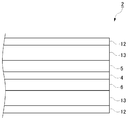
- FIG. 3 is a cross-sectional view of the bent portion of the flexible printed wiring board in the embodiment of the present invention.
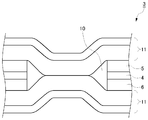
- FIG. 4 is a cross-sectional view of the non-bent portion (through hole portion) of the flexible printed wiring board according to the embodiment of the present invention.
- FIG. 5 is an explanatory diagram of the mesh structure of the flexible printed wiring board in the embodiment of the present invention.
- FIG. 6 is a diagram showing the relationship between the number of layers of a flexible printed circuit board and bending characteristics.
- FIG. 7 is a sectional view of a bent portion of a conventional flexible printed circuit board (comparative example).
- the flexible printed wiring board of the present invention includes a plurality of metal film layers and an insulating layer provided between the plurality of metal film layers, and has a bent portion that requires flexibility and a non-bend that does not require flexibility.
- the metal film layer is not plated, and the non-bent part is provided with through holes that penetrate the plurality of metal film layers.
- a conductive film is affixed from both sides to the portion where the hole is provided, and the conductive film is in contact with the inside of the through hole, whereby the plurality of metal film layers are electrically connected.
- This configuration improves the bending characteristics of the flexible printed wiring board because the metal film layer is not plated.
- a conductive film is used for electrical connection between the metal film layers.
- the metal film layer is electrically connected by attaching a conductive film to the through hole of the non-bent portion and bringing the conductive film into contact with the inside of the through hole. Since this conductive film is affixed to the non-bent part, the bending characteristic of the bent part (bending characteristic of the flexible printed wiring board) is not hindered.
- the plurality of metal film layers include at least one signal line layer and at least one ground line layer, and the ground line layer has a mesh structure for adjusting characteristic impedance. You may have the structure comprised.
- This configuration allows the characteristic impedance to be adjusted by making the ground line layer a mesh structure, and enables high-speed signal transmission using LVDS.
- the mesh structure may have a configuration having a line-symmetric pattern around the center line of the bent portion at least in the bent portion.
- the mesh structure may have a configuration in which a mesh central portion to be made a space is embedded at the end of the bent portion.
- a signal line for LVDS is provided in the non-bent part, and a conductive film is not attached to a part in which the signal line for LVDS is provided. May be included.
- This configuration prevents the conductive film from affecting the characteristic impedance and enables high-speed signal transmission using LVDS.
- the electronic device of the present invention includes the flexible printed wiring board described above.
- the electronic device of the present invention is an electronic product having a movable part such as a surveillance camera.
- the metal film layer is not plated, the bending characteristics are improved.
- FIGS. 3 and 4 are cross-sectional views of the flexible printed wiring board of the present embodiment.
- the flexible printed wiring board 1 has a bent portion 2 and a non-bent portion 3 according to the design of the electronic device to be mounted.
- the bent part 2 is a part that is required to be flexible in design, for example, a part corresponding to a movable part of an electronic device.
- the non-bending portion 3 is a portion that is not required to be flexible in design, for example, a portion that is connected to a terminal (not shown) of a module of an electronic device.
- the non-bending part 3 says the part by which a flexibility is not requested
- the flexible printed wiring board 1 includes a flexible insulating layer 4 and a signal line layer 5 provided on one surface (for example, the upper surface of FIG. 3) of the insulating layer 4. And a ground line layer 6 provided on the other surface of the insulating layer 4 (for example, the lower surface of FIG. 3).
- the signal line layer 5 and the ground line layer 6 are made of a metal film such as a copper foil, and can also be called a metal film layer.
- the signal line layer 5 is etched so as to form a predetermined circuit pattern. In this case, patterns of normal signal lines 7 and LVDS signal lines 8 are formed (see FIGS. 1 and 2), and the ground line layer 6 is etched to form a mesh structure 9 (see FIG. 1). (See FIG. 5).
- the mesh structure 9 will be described in detail later.
- the signal line layer 5 and the ground line layer 6 are not plated.
- the non-bent portion 3 of the flexible printed circuit board 1 includes a portion where a signal line is provided and a portion where a signal line is not provided, and a portion where a signal line is not provided.
- a through hole 10 is provided.
- the conductive film 11 is affixed to the part provided with the through-hole 10 from both sides (both sides) of the upper surface and the lower surface.
- the conductive films 11 are in contact (adhesion) with each other inside the through hole 10, and the signal line layer 5 and the ground line layer 6 are electrically connected via the conductive film 11. ing.
- the conductive film 11 is not attached to the portion where the signal line 8 for LVDS is provided.
- an anisotropic conductive film 11 (ACF) or the like is used as the conductive film 11 (ACF) or the like.
- the bent portion 2 of the flexible printed wiring board 1 is preferably protected by a cover layer 12.
- the cover layer 12 is provided on the signal line layer 5 and the ground line layer 6 via the adhesive layer 13.
- the cover layer 12 and the adhesive layer 13 have sufficient flexibility and have little influence on the bending characteristics.
- the mesh structure 9 is for adjusting the characteristic impedance so that signals can be transmitted by LVDS.
- the mesh structure 9 has a pattern in which meshes (diamond portions in FIG. 5) are arranged symmetrically about the center line of the bent portion 2 (dotted line in FIG. 5).
- the mesh structure 9 has a pattern in which a mesh central portion (a triangular portion in FIG. 5) to be a space is buried at the end portion.
- the mesh structure 9 may be formed on the entire flexible printed wiring board 1 or may be formed only on the bent portion 2.
- the metal film layer is not plated, the bending characteristics of the flexible printed wiring board 1 are improved.
- FIG. 6 is a diagram showing the relationship between the number of layers of the flexible printed wiring board 1 and the bending characteristics.
- the flexible printed wiring board 1 has lower bending characteristics as the number of layers (the number of metal wire layers) increases.
- the thickness of the plating layer 20 is approximately the same as that of the metal line layers 5 and 6. It is necessary to make it thick (see FIG. 7). Therefore, when the number of layers (the number of metal wire layers) is increased, the thickness of the plating layer 20 is also increased correspondingly, and the bending characteristics are remarkably deteriorated.
- the bending characteristics are improved accordingly.
- the conventional technique can provide only a low bending characteristic because the plating layer 20 exists, but in the present invention, since there is no plating layer, the high bending characteristic (substantially the metal wire layer is not present). Two layers of bending properties) are obtained. That is, in the present invention, even when the number of layers is “2”, it is possible to obtain bending characteristics (high bending characteristics) close to the conventional number of layers “1”.
- the conductive film 11 is used for electrical connection between the metal film layers.
- the metal film layer is electrically connected by attaching the conductive film 11 to the through hole 10 of the non-bent portion 3 and bringing the conductive film 11 into contact with the inside of the through hole 10. Since this conductive film 11 is affixed to the non-bending part 3, the bending characteristic of the bending part 2 (the bending characteristic of the flexible printed wiring board 1) is not hindered.
- the ground line layer 6 has a mesh structure 9, whereby the characteristic impedance can be adjusted, and high-speed signal transmission using LVDS becomes possible.
- the stress applied to the bent portion 2 is equalized (symmetrized) when the flexible printed wiring board 1 is bent and stretched. Therefore, it is possible to prevent disconnection due to stress distortion, and the bending characteristics of the flexible printed wiring board 1 are improved.
- the flexible printed wiring board 1 since the mesh pattern by which the mesh center part was embedded in the edge part of the bending part 2 is employ
- the conductive film 11 is not attached to the portion where the signal line 8 for LVDS is provided, the influence on the characteristic impedance by the conductive film 11 can be prevented, and the LVDS is reduced. Utilizing high-speed signal transmission becomes possible.
- the signal line layer and the ground line layer is one layer has been described.
- the signal line layer may be two or more layers.
- the flexible printed wiring board according to the present invention has an effect of high bending characteristics, and is useful when applied to an electronic product having a movable part such as a surveillance camera.
Landscapes
- Engineering & Computer Science (AREA)
- Microelectronics & Electronic Packaging (AREA)
- Structure Of Printed Boards (AREA)
- Printing Elements For Providing Electric Connections Between Printed Circuits (AREA)
Abstract
フレキシブルプリント配線基板(1)は、複数の金属膜層(5、6)と、複数の金属膜層(5、6)の間に設けられた絶縁層(4)とを備える。このフレキシブルプリント配線基板(1)は、屈曲性が要求される屈曲部(2)と、屈曲性が要求されない非屈曲部(3)とで構成される。金属膜層(5、6)には、めっき処理が施されていない。非屈曲部(3)には、複数の金属膜層(5、6)を貫通する貫通孔(10)が設けられ、貫通孔(10)が設けられた部分には、両面から導電フィルム(11)が貼り付けられる。導電フィルム(11)が貫通孔(10)の内部で接触することにより、複数の金属膜層(5、6)が電気的に接続されている。これにより、屈曲特性の高いフレキシブルプリント配線基板が提供される。
Description
本発明は、屈曲特性を向上したフレキシブルプリント配線基板および電子機器に関するものである。
フレキシブルプリント配線基板は、電子機器の可動部の配線に用いられる。そのため、フレキシブルプリント配線基板には、高い屈曲特性が要求される。例えば、監視カメラのパン・チルト機構などでは、屈曲試験で370万往復以上の曲げ伸ばしに耐える屈曲特性が要求される。
ところで、近年、電子機器に多彩な機能が搭載されるようになってきており、電子機器の機種によっては、高速の信号伝送が要求されることがある。このような要求に対して、従来、LVDS(Low Voltage Differential Signaling)をフレキシブルプリント配線板で利用する方法が提案されている(例えば、特許文献1参照)。
この従来の手法では、フレキシブルプリント配線板を多層化して、2つの金属線層(信号線層とグランド線層)の間に絶縁層を設け、グランド線層をメッシュ構造にして特性インピーダンスを調整することで、LVDSによる高速伝送を可能にしている。そして、従来のフレキシブルプリント配線板では、2つの金属線層(信号線層とグランド線層)に、めっき処理が施され、スルーホールを介して、信号線層とグランド線層を電気的に接続している。
しかしながら、従来の手法では、フレキシブルプリント配線基板を多層化するため、その分だけ屈曲特性が低下してしまう。特に、金属線層(信号線層やグランド線層)にめっき処理を施している場合には、屈曲特性の低下が著しかった。
例えば、LVDSの信号線層とグランド線層を電気的に接続するためにめっき処理を施す場合には、めっき層の厚みを金属線層と同程度の厚みにする必要がある。フレキシブルプリント配線板の屈曲特性は、金属線層やめっき層の厚みに大きく依存する。そのため、2層の金属線層にそれぞれめっき処理を施した場合には、実質的に金属線層がそれぞれ2層分の厚さになったのと同程度の影響がでることになり、その結果、屈曲特性が著しく低下してしまうことになる。
本発明は、上記背景の下でなされたものである。本発明の目的は、屈曲特性を向上することのできるフレキシブルプリント配線基板を提供することにある。
本発明の一の態様は、フレキシブルプリント配線基板であり、このフレキシブルプリント配線基板は、複数の金属膜層と、複数の金属膜層の間に設けられた絶縁層とを備え、屈曲性が要求される屈曲部と、屈曲性が要求されない非屈曲部とで構成され、金属膜層には、めっき処理が施されておらず、非屈曲部には、複数の金属膜層を貫通する貫通孔が設けられており、貫通孔が設けられた部分には、両面から導電フィルムが貼り付けられ、導電フィルムが貫通孔の内部で接触することにより、複数の金属膜層が電気的に接続されている。
本発明の別の態様は、電子機器であり、この電子機器は、上記のフレキシブルプリント配線基板を備えている。
以下に説明するように、本発明には他の態様が存在する。したがって、この発明の開示は、本発明の一部の態様の提供を意図しており、ここで記述され請求される発明の範囲を制限することは意図していない。
以下に本発明の詳細な説明を述べる。ただし、以下の詳細な説明と添付の図面は発明を限定するものではない。
本発明のフレキシブルプリント配線基板は、複数の金属膜層と、複数の金属膜層の間に設けられた絶縁層とを備え、屈曲性が要求される屈曲部と、屈曲性が要求されない非屈曲部とで構成されたフレキシブルプリント配線基板において、金属膜層には、めっき処理が施されておらず、非屈曲部には、複数の金属膜層を貫通する貫通孔が設けられており、貫通孔が設けられた部分には、両面から導電フィルムが貼り付けられ、導電フィルムが貫通孔の内部で接触することにより、複数の金属膜層が電気的に接続された構成を有している。
この構成により、金属膜層にめっき処理が施されていないので、フレキシブルプリント配線基板の屈曲特性が向上する。この場合、金属膜層の間の電気的な接続には、導電フィルムが利用される。具体的には、非屈曲部の貫通孔に導電フィルムを貼り付け、貫通孔の内部で導電フィルムを接触させることにより、金属膜層が電気的に接続される。この導電フィルムは、非屈曲部に貼り付けられるので、屈曲部の屈曲特性(フレキシブルプリント配線基板の屈曲特性)を阻害することがない。
また、本発明のフレキシブルプリント配線基板では、複数の金属膜層は、少なくとも1つの信号線層と、少なくとも1つのグランド線層を含み、グランド線層は、特性インピーダンスを調整するためにメッシュ構造とされた構成を有してよい。
この構成により、グランド線層をメッシュ構造にすることにより、特性インピーダンスを調整することができ、LVDSを利用した高速の信号伝送が可能になる。
また、本発明のフレキシブルプリント配線基板では、メッシュ構造は、少なくとも屈曲部において、屈曲部の中央線を中心として線対称のパターンを有する構成を有してよい。
この構成により、フレキシブルプリント配線基板が曲げ伸ばしされるときに、屈曲部にかかる応力が均等化(対称化)され、応力の歪みによって断線するのを防ぐことができ、フレキシブルプリント配線基板の屈曲特性が向上する。
また、本発明のフレキシブルプリント配線基板では、メッシュ構造は、屈曲部の端部において、空間とされるべきメッシュ中央部が埋められたパターンを有する構成を有してよい。
この構成により、屈曲部の端部の強度が高くなるので、フレキシブルプリント配線基板が曲げ伸ばしされるときの負荷を、端部(強度の高い部分)で受けることができ、したがって、フレキシブルプリント配線基板の屈曲特性が向上する。
また、本発明のフレキシブルプリント配線基板では、非屈曲部には、LVDS用の信号線が設けられており、LVDS用の信号線が設けられた部分には、導電フィルムが貼り付けられていない構成を有してよい。
この構成により、導電フィルムによる特性インピーダンスへの影響を防ぐことができ、LVDSを利用した高速の信号伝送が可能になる。
本発明の電子機器は、上記のフレキシブルプリント配線基板を備えている。本発明の電子機器は、例えば、監視カメラなどの可動部を有する電子製品である。
本発明では、金属膜層にめっき処理が施されていないので屈曲特性が向上する。
以下、本発明の実施の形態のフレキシブルプリント配線基板について、図面を用いて説明する。本実施の形態では、監視カメラなどの可動部を有する電子製品等に用いられるフレキシブルプリント配線基板の場合を例示する。
本発明の実施の形態のフレキシブルプリント配線基板の構成を、図面を参照して説明する。図1および図2は、本実施の形態のフレキシブルプリント配線基板の平面図であり、図3および図4は、本実施の形態のフレキシブルプリント配線基板の断面図である。
図1および図2に示すように、フレキシブルプリント配線基板1は、実装される電子機器の設計に応じて屈曲部2と非屈曲部3を有している。屈曲部2は、設計上、屈曲性が要求される部分であり、例えば、電子機器の可動部分に相当する部分である。非屈曲部3は、設計上、屈曲性が要求されない部分であり、例えば、電子機器のモジュールの端子(図示せず)に接続される部分である。なお、非屈曲部3は、設計上、屈曲性が要求されない部分をいうが、ある程度の屈曲性を有してよいことはいうまでもない。
図3および図4に示すように、フレキシブルプリント配線基板1は、可撓性を有する絶縁層4と、絶縁層4の一方の面(例えば、図3の上面)に設けられた信号線層5と、絶縁層4の他方の面(例えば、図3の下面)に設けられたグランド線層6を備えている。信号線層5とグランド線層6は、銅箔などの金属膜で構成されており、金属膜層と呼ぶこともできる。信号線層5は、所定の回路パターンを形成するようにエッチングされている。この場合、通常の信号線7とLVDS用の信号線8のパターンが形成されている(図1および図2参照)、グランド線層6は、メッシュ構造9を形成するようにエッチングされている(図5参照)。このメッシュ構造9については、後で詳しく説明する。この信号線層5とグランド線層6には、めっき処理が施されていない。
図2に示すように、フレキシブルプリント配線基板1の非屈曲部3には、信号線が設けられた部分と、信号線が設けられていない部分があり、信号線が設けられていない部分には、貫通孔10が設けられている。図1に示すように、貫通孔10が設けられた部分には、上面と下面の両側(両面)から導電フィルム11が貼り付けられている。図4に示すように、導電フィルム11は、貫通孔10の内部で互いに接触(接着)しており、この導電フィルム11を介して、信号線層5とグランド線層6が電気的に接続されている。なお、図1に示すように、導電フィルム11は、LVDS用の信号線8が設けられた部分には、貼り付けられていない。導電フィルム11としては、異方性導電フィルム11(ACF)などが用いられる。
図3に示すように、フレキシブルプリント配線基板1の屈曲部2は、カバー層12で保護されているのが好ましい。この場合、信号線層5やグランド線層6の上に、接着剤層13を介してカバー層12が設けられる。このカバー層12や接着剤層13は、十分な可撓性を有しており、屈曲特性に与える影響は小さい。
ここで、グランド線層6のメッシュ構造9について説明する。メッシュ構造9は、LVDSで信号伝送することができるように、特性インピーダンスを調整するためのものである。図5に示すように、メッシュ構造9は、屈曲部2の中央線(図5の点線)を中心として線対称にメッシュ(図5では、菱形の部分)が並んだパターンを有している。また、メッシュ構造9は、端部において、空間とされるべきメッシュ中央部(図5では、三角形の部分)が埋められたパターンを有している。なお、このメッシュ構造9は、フレキシブルプリント配線基板1の全体に形成されていてもよく、屈曲部2の部分だけに形成されていてもよい。
このような本実施の形態のフレキシブルプリント配線基板1によれば、金属膜層にめっき処理が施されていないので、フレキシブルプリント配線基板1の屈曲特性が向上する。
図6は、フレキシブルプリント配線基板1の層数と屈曲特性との関係を示す図である。図6に示すように、フレキシブルプリント配線基板1は、層数(金属線層の層数)が増えていくと、屈曲特性が低下する。特に、従来のように、LVDSの信号線層5とグランド線層6を電気的に接続するためにめっき処理を施す場合には、めっき層20の厚みを金属線層5、6と同程度の厚みにする必要がある(図7参照)。そのため、層数(金属線層の層数)が増えると、その分、めっき層20の厚みも増加し、屈曲特性が著しく低下することになる。
これに対して、本実施の形態のフレキシブルプリント配線基板1では、同じ層数(金属線層の層数)であっても、めっき層が存在していないので、その分だけ、屈曲特性が向上する。例えば、層数「2」の場合、従来の技術ではめっき層20が存在するので低い屈曲特性しか得られないが、本発明ではめっき層が存在しないので高い屈曲特性(実質的に金属線層が2層の屈曲特性)が得られる。すなわち、本発明では、層数「2」の場合であっても、従来の層数「1」に近い屈曲特性(高い屈曲特性)を得ることができる。
本実施の形態では、金属膜層の間の電気的な接続には、導電フィルム11が利用される。具体的には、非屈曲部3の貫通孔10に導電フィルム11を貼り付け、貫通孔10の内部で導電フィルム11を接触させることにより、金属膜層が電気的に接続される。この導電フィルム11は、非屈曲部3に貼り付けられるので、屈曲部2の屈曲特性(フレキシブルプリント配線基板1の屈曲特性)を阻害することがない。
また、本実施の形態では、グランド線層6をメッシュ構造9にすることにより、特性インピーダンスを調整することができ、LVDSを利用した高速の信号伝送が可能になる。
また、本実施の形態では、屈曲部2において線対称のメッシュパターンを採用しているので、フレキシブルプリント配線基板1が曲げ伸ばしされるときに、屈曲部2にかかる応力が均等化(対称化)され、応力の歪みによって断線するのを防ぐことができ、フレキシブルプリント配線基板1の屈曲特性が向上する。
また、本実施の形態では、屈曲部2の端部においてメッシュ中央部が埋められたメッシュパターンを採用しているので、屈曲部2の端部の強度が高くなるので、フレキシブルプリント配線基板1が曲げ伸ばしされるときの負荷を、端部(強度の高い部分)で受けることができ、したがって、フレキシブルプリント配線基板1の屈曲特性が向上する。
また、本実施の形態では、LVDS用の信号線8が設けられた分には、導電フィルム11が貼り付けられていないので、導電フィルム11による特性インピーダンスへの影響を防ぐことができ、LVDSを利用した高速の信号伝送が可能になる。
以上、本発明の実施の形態を例示により説明したが、本発明の範囲はこれらに限定されるものではなく、請求項に記載された範囲内において目的に応じて変更・変形することが可能である。
例えば、以上の説明では、信号線層とグランド線層がそれぞれ1層である場合について説明したが、さらに信号数が多い場合には、信号線層が2層以上であってもよい。
以上に現時点で考えられる本発明の好適な実施の形態を説明したが、本実施の形態に対して多様な変形が可能なことが理解され、そして、本発明の真実の精神と範囲内にあるそのようなすべての変形を添付の請求の範囲が含むことが意図されている。
以上のように、本発明にかかるフレキシブルプリント配線基板は、屈曲特性が高いという効果を有し、監視カメラなどの可動部を有する電子製品等に適用され、有用である。
1 フレキシブルプリント配線基板
2 屈曲部
3 非屈曲部
4 絶縁層
5 信号線層
6 グランド線層
7 通常の信号線
8 LVDS用の信号線
9 メッシュ構造
10 貫通孔
11 導電フィルム
12 カバー層
13 接着剤層
20 めっき層
2 屈曲部
3 非屈曲部
4 絶縁層
5 信号線層
6 グランド線層
7 通常の信号線
8 LVDS用の信号線
9 メッシュ構造
10 貫通孔
11 導電フィルム
12 カバー層
13 接着剤層
20 めっき層
Claims (6)
- 複数の金属膜層と、前記複数の金属膜層の間に設けられた絶縁層とを備え、
屈曲性が要求される屈曲部と、屈曲性が要求されない非屈曲部とで構成されたフレキシブルプリント配線基板において、
前記金属膜層には、めっき処理が施されておらず、
前記非屈曲部には、前記複数の金属膜層を貫通する貫通孔が設けられており、
前記貫通孔が設けられた部分には、両面から導電フィルムが貼り付けられ、前記導電フィルムが前記貫通孔の内部で接触することにより、前記複数の金属膜層が電気的に接続されていることを特徴とするフレキシブルプリント配線基板。 - 前記複数の金属膜層は、少なくとも1つの信号線層と、少なくとも1つのグランド線層を含み、前記グランド線層は、特性インピーダンスを調整するためにメッシュ構造とされていることを特徴とする請求項1に記載のフレキシブルプリント配線基板。
- 前記メッシュ構造は、少なくとも前記屈曲部において、前記屈曲部の中央線を中心として線対称のパターンを有することを特徴とする請求項2に記載のフレキシブルプリント配線基板。
- 前記メッシュ構造は、前記屈曲部の端部において、空間とされるべきメッシュ中央部が埋められたパターンを有する請求項3に記載のフレキシブルプリント配線基板。
- 前記非屈曲部には、LVDS用の信号線が設けられており、
前記LVDS用の信号線が設けられた部分には、前記導電フィルムが貼り付けられていないことを特徴とする請求項1に記載のフレキシブルプリント配線基板。 - 請求項1に記載のフレキシブルプリント配線基板を備えた電子機器。
Applications Claiming Priority (2)
| Application Number | Priority Date | Filing Date | Title |
|---|---|---|---|
| JP2010176305A JP2012038851A (ja) | 2010-08-05 | 2010-08-05 | フレキシブルプリント配線基板 |
| JP2010-176305 | 2010-08-05 |
Publications (1)
| Publication Number | Publication Date |
|---|---|
| WO2012017664A1 true WO2012017664A1 (ja) | 2012-02-09 |
Family
ID=45559183
Family Applications (1)
| Application Number | Title | Priority Date | Filing Date |
|---|---|---|---|
| PCT/JP2011/004428 Ceased WO2012017664A1 (ja) | 2010-08-05 | 2011-08-04 | フレキシブルプリント配線基板および電子機器 |
Country Status (2)
| Country | Link |
|---|---|
| JP (1) | JP2012038851A (ja) |
| WO (1) | WO2012017664A1 (ja) |
Cited By (2)
| Publication number | Priority date | Publication date | Assignee | Title |
|---|---|---|---|---|
| CN111866334A (zh) * | 2019-04-25 | 2020-10-30 | 佳能株式会社 | 配备有柔性板的电子设备 |
| CN117395855A (zh) * | 2023-10-25 | 2024-01-12 | 荣耀终端有限公司 | 柔性电路板及电子设备 |
Citations (7)
| Publication number | Priority date | Publication date | Assignee | Title |
|---|---|---|---|---|
| JPH10341065A (ja) * | 1997-06-06 | 1998-12-22 | Sony Corp | 補強板付きプリント配線板 |
| JP2000269632A (ja) * | 1999-03-17 | 2000-09-29 | Tatsuta Electric Wire & Cable Co Ltd | シールドフレキシブルプリント配線板の製造方法、シールドフレキシブルプリント配線板用補強シールドフィルム及びシールドフレキシブルプリント配線板 |
| JP2003258387A (ja) * | 2002-03-06 | 2003-09-12 | Sumitomo Electric Printed Circuit Inc | 両面フレキシブルプリント回路 |
| JP2006024824A (ja) * | 2004-07-09 | 2006-01-26 | Tatsuta System Electronics Kk | インピーダンスコントロールフィルム、インピーダンスコントロールシールドフィルム及びそれを用いた配線板 |
| JP2007207997A (ja) * | 2006-02-01 | 2007-08-16 | Sumitomo Bakelite Co Ltd | 回路基板 |
| JP2007281145A (ja) * | 2006-04-05 | 2007-10-25 | Kenwood Corp | フレキシブル配線体 |
| JP2009099773A (ja) * | 2007-10-17 | 2009-05-07 | Fujikura Ltd | シールド付回路配線基板 |
-
2010
- 2010-08-05 JP JP2010176305A patent/JP2012038851A/ja active Pending
-
2011
- 2011-08-04 WO PCT/JP2011/004428 patent/WO2012017664A1/ja not_active Ceased
Patent Citations (7)
| Publication number | Priority date | Publication date | Assignee | Title |
|---|---|---|---|---|
| JPH10341065A (ja) * | 1997-06-06 | 1998-12-22 | Sony Corp | 補強板付きプリント配線板 |
| JP2000269632A (ja) * | 1999-03-17 | 2000-09-29 | Tatsuta Electric Wire & Cable Co Ltd | シールドフレキシブルプリント配線板の製造方法、シールドフレキシブルプリント配線板用補強シールドフィルム及びシールドフレキシブルプリント配線板 |
| JP2003258387A (ja) * | 2002-03-06 | 2003-09-12 | Sumitomo Electric Printed Circuit Inc | 両面フレキシブルプリント回路 |
| JP2006024824A (ja) * | 2004-07-09 | 2006-01-26 | Tatsuta System Electronics Kk | インピーダンスコントロールフィルム、インピーダンスコントロールシールドフィルム及びそれを用いた配線板 |
| JP2007207997A (ja) * | 2006-02-01 | 2007-08-16 | Sumitomo Bakelite Co Ltd | 回路基板 |
| JP2007281145A (ja) * | 2006-04-05 | 2007-10-25 | Kenwood Corp | フレキシブル配線体 |
| JP2009099773A (ja) * | 2007-10-17 | 2009-05-07 | Fujikura Ltd | シールド付回路配線基板 |
Cited By (4)
| Publication number | Priority date | Publication date | Assignee | Title |
|---|---|---|---|---|
| CN111866334A (zh) * | 2019-04-25 | 2020-10-30 | 佳能株式会社 | 配备有柔性板的电子设备 |
| CN111866334B (zh) * | 2019-04-25 | 2022-02-11 | 佳能株式会社 | 配备有柔性板的电子设备 |
| CN117395855A (zh) * | 2023-10-25 | 2024-01-12 | 荣耀终端有限公司 | 柔性电路板及电子设备 |
| CN117395855B (zh) * | 2023-10-25 | 2024-12-13 | 荣耀终端有限公司 | 柔性电路板及电子设备 |
Also Published As
| Publication number | Publication date |
|---|---|
| JP2012038851A (ja) | 2012-02-23 |
Similar Documents
| Publication | Publication Date | Title |
|---|---|---|
| US7067912B2 (en) | Wired circuit board | |
| TWI665943B (zh) | 多層撓性印刷配線板及其製造方法 | |
| CN103514996B (zh) | 复合式软性电路排线 | |
| KR101317897B1 (ko) | 브리지 공법을 이용한 루프안테나 양면 회로 형성 방법 | |
| CN102316664A (zh) | 柔性电路板及其制作方法 | |
| JPWO2006100764A1 (ja) | プリント配線板 | |
| JP2017539095A (ja) | フレキシブルプリント配線板、これを含む電子装置、およびフレキシブルプリント配線板の製造方法 | |
| JP2013051387A (ja) | 電子回路板 | |
| CN207802499U (zh) | 柔性电路板 | |
| JP4414365B2 (ja) | 高速伝送用基板 | |
| WO2012017664A1 (ja) | フレキシブルプリント配線基板および電子機器 | |
| CN101877936B (zh) | 布线电路基板 | |
| US20170064829A1 (en) | Conductor connecting structure and mounting board | |
| JP2013157490A (ja) | 両面フレキシブルプリント基板及び両面フレキシブルプリント基板用コネクタ | |
| JP2008235697A (ja) | 配線回路基板およびその製造方法 | |
| JP4933170B2 (ja) | プリント回路基板アセンブリー | |
| JP2017045882A (ja) | フレキシブル基板及びその製造方法並びに電子装置 | |
| JP2010016076A (ja) | フレキシブルプリント基板及びこれを備えたリジッドフレキシブルプリント基板 | |
| JP4998741B2 (ja) | アダプタ構造,高周波ケーブル体および配線板接続体 | |
| KR101050876B1 (ko) | 연성인쇄회로기판의 제조방법 및 그 연성인쇄회로기판 | |
| JP4907281B2 (ja) | フレキシブル配線回路基板 | |
| CN106413240A (zh) | 布线电路基板及其制造方法 | |
| JP4793230B2 (ja) | フレキシブルプリント基板 | |
| KR101098369B1 (ko) | 연성 평판 케이블을 이용한 저전압 차등 신호 케이블 | |
| JP2005142425A (ja) | フレキシブル配線板及びこれを用いた電子機器 |
Legal Events
| Date | Code | Title | Description |
|---|---|---|---|
| 121 | Ep: the epo has been informed by wipo that ep was designated in this application |
Ref document number: 11814299 Country of ref document: EP Kind code of ref document: A1 |
|
| NENP | Non-entry into the national phase |
Ref country code: DE |
|
| 122 | Ep: pct application non-entry in european phase |
Ref document number: 11814299 Country of ref document: EP Kind code of ref document: A1 |