WO2012014865A1 - 表示装置およびその駆動方法 - Google Patents
表示装置およびその駆動方法 Download PDFInfo
- Publication number
- WO2012014865A1 WO2012014865A1 PCT/JP2011/066903 JP2011066903W WO2012014865A1 WO 2012014865 A1 WO2012014865 A1 WO 2012014865A1 JP 2011066903 W JP2011066903 W JP 2011066903W WO 2012014865 A1 WO2012014865 A1 WO 2012014865A1
- Authority
- WO
- WIPO (PCT)
- Prior art keywords
- switching element
- sensor pixel
- storage node
- pixel circuit
- period
- Prior art date
- Legal status (The legal status is an assumption and is not a legal conclusion. Google has not performed a legal analysis and makes no representation as to the accuracy of the status listed.)
- Ceased
Links
Images
















Classifications
-
- G—PHYSICS
- G06—COMPUTING OR CALCULATING; COUNTING
- G06F—ELECTRIC DIGITAL DATA PROCESSING
- G06F3/00—Input arrangements for transferring data to be processed into a form capable of being handled by the computer; Output arrangements for transferring data from processing unit to output unit, e.g. interface arrangements
- G06F3/01—Input arrangements or combined input and output arrangements for interaction between user and computer
- G06F3/03—Arrangements for converting the position or the displacement of a member into a coded form
- G06F3/041—Digitisers, e.g. for touch screens or touch pads, characterised by the transducing means
- G06F3/0416—Control or interface arrangements specially adapted for digitisers
- G06F3/04164—Connections between sensors and controllers, e.g. routing lines between electrodes and connection pads
-
- G—PHYSICS
- G06—COMPUTING OR CALCULATING; COUNTING
- G06F—ELECTRIC DIGITAL DATA PROCESSING
- G06F3/00—Input arrangements for transferring data to be processed into a form capable of being handled by the computer; Output arrangements for transferring data from processing unit to output unit, e.g. interface arrangements
- G06F3/01—Input arrangements or combined input and output arrangements for interaction between user and computer
- G06F3/03—Arrangements for converting the position or the displacement of a member into a coded form
- G06F3/041—Digitisers, e.g. for touch screens or touch pads, characterised by the transducing means
- G06F3/0412—Digitisers structurally integrated in a display
-
- G—PHYSICS
- G09—EDUCATION; CRYPTOGRAPHY; DISPLAY; ADVERTISING; SEALS
- G09G—ARRANGEMENTS OR CIRCUITS FOR CONTROL OF INDICATING DEVICES USING STATIC MEANS TO PRESENT VARIABLE INFORMATION
- G09G5/00—Control arrangements or circuits for visual indicators common to cathode-ray tube indicators and other visual indicators
- G09G5/003—Details of a display terminal, the details relating to the control arrangement of the display terminal and to the interfaces thereto
-
- G—PHYSICS
- G02—OPTICS
- G02F—OPTICAL DEVICES OR ARRANGEMENTS FOR THE CONTROL OF LIGHT BY MODIFICATION OF THE OPTICAL PROPERTIES OF THE MEDIA OF THE ELEMENTS INVOLVED THEREIN; NON-LINEAR OPTICS; FREQUENCY-CHANGING OF LIGHT; OPTICAL LOGIC ELEMENTS; OPTICAL ANALOGUE/DIGITAL CONVERTERS
- G02F1/00—Devices or arrangements for the control of the intensity, colour, phase, polarisation or direction of light arriving from an independent light source, e.g. switching, gating or modulating; Non-linear optics
- G02F1/01—Devices or arrangements for the control of the intensity, colour, phase, polarisation or direction of light arriving from an independent light source, e.g. switching, gating or modulating; Non-linear optics for the control of the intensity, phase, polarisation or colour
- G02F1/13—Devices or arrangements for the control of the intensity, colour, phase, polarisation or direction of light arriving from an independent light source, e.g. switching, gating or modulating; Non-linear optics for the control of the intensity, phase, polarisation or colour based on liquid crystals, e.g. single liquid crystal display cells
- G02F1/133—Constructional arrangements; Operation of liquid crystal cells; Circuit arrangements
- G02F1/13306—Circuit arrangements or driving methods for the control of single liquid crystal cells
- G02F1/13312—Circuits comprising photodetectors for purposes other than feedback
-
- G—PHYSICS
- G02—OPTICS
- G02F—OPTICAL DEVICES OR ARRANGEMENTS FOR THE CONTROL OF LIGHT BY MODIFICATION OF THE OPTICAL PROPERTIES OF THE MEDIA OF THE ELEMENTS INVOLVED THEREIN; NON-LINEAR OPTICS; FREQUENCY-CHANGING OF LIGHT; OPTICAL LOGIC ELEMENTS; OPTICAL ANALOGUE/DIGITAL CONVERTERS
- G02F1/00—Devices or arrangements for the control of the intensity, colour, phase, polarisation or direction of light arriving from an independent light source, e.g. switching, gating or modulating; Non-linear optics
- G02F1/01—Devices or arrangements for the control of the intensity, colour, phase, polarisation or direction of light arriving from an independent light source, e.g. switching, gating or modulating; Non-linear optics for the control of the intensity, phase, polarisation or colour
- G02F1/13—Devices or arrangements for the control of the intensity, colour, phase, polarisation or direction of light arriving from an independent light source, e.g. switching, gating or modulating; Non-linear optics for the control of the intensity, phase, polarisation or colour based on liquid crystals, e.g. single liquid crystal display cells
- G02F1/133—Constructional arrangements; Operation of liquid crystal cells; Circuit arrangements
- G02F1/1333—Constructional arrangements; Manufacturing methods
- G02F1/13338—Input devices, e.g. touch panels
-
- G—PHYSICS
- G06—COMPUTING OR CALCULATING; COUNTING
- G06F—ELECTRIC DIGITAL DATA PROCESSING
- G06F3/00—Input arrangements for transferring data to be processed into a form capable of being handled by the computer; Output arrangements for transferring data from processing unit to output unit, e.g. interface arrangements
- G06F3/01—Input arrangements or combined input and output arrangements for interaction between user and computer
- G06F3/03—Arrangements for converting the position or the displacement of a member into a coded form
- G06F3/041—Digitisers, e.g. for touch screens or touch pads, characterised by the transducing means
- G06F3/042—Digitisers, e.g. for touch screens or touch pads, characterised by the transducing means by opto-electronic means
Definitions
- the present invention relates to a display device, and more particularly to a display device in which a plurality of photosensors are arranged in a pixel region.
- a method for providing an input function such as a touch panel, a pen input, and a scanner by providing a display panel with a plurality of optical sensors is known.
- an optical sensor as shown in FIG. 33, a circuit configuration including a photodiode PD1, a capacitor C INT, and a transistor M1 is known (International Publication No. 2007/145346 and International Publication). No. 2007/145347).
- the gate of the transistor M1 is connected to the storage node INT.
- the storage node INT is connected to one electrode of the capacitor C INT and one electrode (cathode) of the photodiode PD1.
- the other electrode (anode) of the photodiode PD1 is connected to the reset line RST.
- the other electrode of the capacitor C INT is connected to the readout wiring RWS.
- the operation of the conventional optical sensor is as follows. First, in the reset period, a voltage for applying a forward bias to the photodiode PD1 is supplied to the reset line RST. Thereby, in the reset period, the storage node INT is reset to a predetermined potential. When the reset period ends, a voltage for applying a reverse bias to the photodiode PD1 is supplied to the reset line RST. In the accumulation period following the reset period, charge accumulation to the accumulation node INT is performed. In a readout period subsequent to the accumulation period, by applying a read voltage to the readout wiring RWS, the charge accumulated in the accumulation period is read from the accumulation node INT by the transistor M1.
- An object of the present invention is to solve the above problems and provide a display device with a photosensor with improved sensitivity.
- a display device disclosed herein supplies a drive signal to a display panel including a plurality of display pixel circuits and a plurality of sensor pixel circuits in a display region, and the sensor pixel circuits.
- a drive circuit, and the sensor pixel circuit includes a light receiving element, a storage node that holds a charge corresponding to the amount of light incident on the light receiving element, and a read switching element connected to the storage node,
- the configuration further includes a first switching element connected between the element and the storage node and operating in a saturation region, and a second switching element for resetting the storage node.
- a display device with an optical sensor with improved sensitivity can be provided.
- FIG. 1 is a block diagram showing a configuration of a display device according to an embodiment of the present invention.
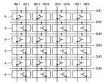
- FIG. 2 is a diagram showing an arrangement of sensor pixel circuits in a display panel included in the display device shown in FIG.
- FIG. 3 is a circuit diagram showing a specific configuration of the sensor pixel circuit according to the first embodiment.
- FIG. 4 is a waveform diagram of a drive signal for driving the sensor pixel circuit according to the first embodiment.
- FIG. 5 is a waveform diagram showing changes in various signals of the sensor pixel circuit in the vicinity of times ta to tc shown in FIG.
- FIG. 6A is a schematic diagram illustrating the operation of the sensor pixel circuit when the drive signals illustrated in FIGS. 4 and 5 are supplied.
- FIG. 1 is a block diagram showing a configuration of a display device according to an embodiment of the present invention.
- FIG. 2 is a diagram showing an arrangement of sensor pixel circuits in a display panel included in the display device shown in FIG.
- FIG. 3 is
- FIG. 6B is a schematic diagram illustrating the operation of the sensor pixel circuit when the drive signals illustrated in FIGS. 4 and 5 are supplied.
- FIG. 6C is a schematic diagram illustrating the operation of the sensor pixel circuit when the drive signals illustrated in FIGS. 4 and 5 are supplied.
- FIG. 7 is a circuit diagram showing a configuration of a modified example of the sensor pixel circuit according to the first embodiment.
- FIG. 8 is a circuit diagram showing a configuration of a modified example of the sensor pixel circuit according to the first embodiment.
- FIG. 9 is a circuit diagram showing a configuration of a modified example of the sensor pixel circuit according to the first embodiment.
- FIG. 10 is a circuit diagram showing a configuration of a modification of the sensor pixel circuit according to the first embodiment.
- FIG. 11 is a circuit diagram showing a configuration of a modification of the sensor pixel circuit according to the first embodiment.
- FIG. 12 is a circuit diagram showing a configuration of a modification of the sensor pixel circuit according to the first embodiment.
- FIG. 13 is a circuit diagram showing a configuration of a modified example of the sensor pixel circuit according to the first embodiment.
- FIG. 14 is a circuit diagram showing a configuration of a modification of the sensor pixel circuit according to the first embodiment.
- FIG. 15 is a circuit diagram showing a configuration of a modification of the sensor pixel circuit according to the first embodiment.
- FIG. 16 is a circuit diagram illustrating a configuration of a modification of the sensor pixel circuit according to the first embodiment.
- FIG. 17 is a circuit diagram showing a configuration of a modification of the sensor pixel circuit according to the first embodiment.
- FIG. 18 is a circuit diagram showing a configuration of a modification of the sensor pixel circuit according to the first embodiment.
- FIG. 19 is a circuit diagram showing a configuration of a modified example of the sensor pixel circuit according to the first embodiment.
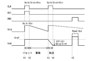
- FIG. 20 is a waveform diagram showing a drive signal applied to the sensor pixel circuit and potential changes of Vsig and Vint in the second embodiment.
- FIG. 21 is a diagram illustrating an arrangement of sensor pixel circuits in the pixel region of the display device according to the third embodiment.
- FIG. 22 is a diagram showing the timing for turning on and off the backlight, and the reset and readout timings for the sensor pixel circuit.
- FIG. 23A is a circuit diagram illustrating an example of a specific configuration of the first sensor pixel circuit according to the third embodiment.
- FIG. 23B is a circuit diagram illustrating an example of a specific configuration of the second sensor pixel circuit according to the third embodiment.
- FIG. 24 is a signal waveform diagram of the display panel according to the third embodiment.
- FIG. 25 is a circuit diagram of a sensor pixel circuit according to the third embodiment.
- FIG. 26 is a circuit diagram showing a configuration of a modified example of the sensor pixel circuit according to the third embodiment.
- FIG. 27 is a circuit diagram illustrating a configuration of a modified example of the sensor pixel circuit according to the third embodiment.
- FIG. 28 is a circuit diagram showing a configuration of a modification of the sensor pixel circuit according to the third embodiment.
- FIG. 29 is a circuit diagram illustrating a configuration of a modified example of the sensor pixel circuit according to the third embodiment.
- FIG. 30 is a circuit diagram showing a configuration of a modification of the sensor pixel circuit according to the third embodiment.
- FIG. 31 is a circuit diagram illustrating a configuration of a modified example of the sensor pixel circuit according to the third embodiment.
- FIG. 32 is a signal waveform diagram of the display panel according to the fourth embodiment.
- FIG. 33 is a circuit diagram showing a configuration of a conventional photosensor.
- a display device includes: A display panel including a plurality of display pixel circuits and a plurality of sensor pixel circuits in a display region; A drive circuit for supplying a drive signal to the sensor pixel circuit,
- the sensor pixel circuit includes: A light receiving element; A first accumulation node for accumulating charges according to the amount of light incident on the light receiving element; A second storage node for holding the charge of the first storage node; A read switching element connected to the second storage node; The first storage node is connected between the first storage node and the second storage node, and operates in a saturation region when transferring the charge stored in the first storage node to the second storage node.
- the sensor pixel circuit comprises: A capacitor connected between the second storage node and the read signal line; A configuration may be adopted in which a reset line is connected to the gate of the second switching element, a constant voltage source is connected to the source, and the second storage node is connected to the drain (second configuration).
- the sensor pixel circuit comprises: A capacitor connected between the second storage node and the read signal line; A configuration may be adopted in which a reset line is connected to the gate of the second switching element, the read signal line is connected to the source, and the second storage node is connected to the drain (third configuration).
- the drive circuit is within a unit period, A reset period for turning on the first switching element and turning on the second switching element to reset the first and second storage nodes; An accumulation period for turning off the first switching element and turning off the second switching element, and accumulating charges according to the amount of light received by the light receiving element at the first accumulation node; A transfer period in which the first switching element is turned on and the second switching element is turned off to transfer the charge accumulated in the accumulation period in the first accumulation node to the second accumulation node; It is preferable that the first switching element is turned off and the second switching element is turned off, and sensing is performed in accordance with a reading period in which reading is performed with the reading switching element turned on (fourth). Constitution).
- the drive circuit is within a unit period, A reset period for turning on the first switching element and turning on the second switching element to reset the first and second storage nodes;
- the first switching element is turned on and the second switching element is turned off to accumulate charges corresponding to the amount of light received by the light receiving element at the first accumulation node, and at the same time, the first switching element
- An accumulation transfer period for transferring charges accumulated in the accumulation period at the accumulation node to the second accumulation node; It is also preferable that sensing be performed in accordance with a reading period in which the first switching element is turned off and the second switching element is turned off, and the reading switching element is turned on and reading is performed (fifth) Constitution).
- the sensor pixel circuit includes a first sensor pixel circuit that detects light during a detection period when the light source is turned on, and a second sensor pixel circuit that detects light during a detection period when the light source is turned off, It is also preferable that the driving circuit read out from the first and second sensor pixel circuits in a line sequential manner other than the detection period when the light source is turned on and the detection period when the light source is turned off (sixth structure). .
- the light source is turned on for a predetermined time once in one frame period, More preferably, the detection period when the light source is turned on and the detection period when the light source is turned off are set once per frame period (seventh structure).
- the first sensor pixel circuit and the second sensor pixel circuit share one photosensor (eighth configuration).
- the first capacitor is a P-type transistor (ninth configuration).
- the sensor pixel circuit comprises: A reference light-receiving element connected in series to the light-receiving element and shielded from light; It is preferable that the first storage node is connected between the light receiving element and the reference light receiving element (tenth structure).
- the light receiving element may be an N-type transistor (an eleventh structure).
- a driving method of a display device is as follows.
- a display panel including a plurality of display pixel circuits and a plurality of sensor pixel circuits in a display region; and a drive circuit that supplies a drive signal to the sensor pixel circuit, wherein the sensor pixel circuit includes a light receiving element; A first storage node for storing charges according to the amount of light incident on the light receiving element; a second storage node for storing charges of the first storage node; and the second storage node connected to the second storage node A read switching element, connected between the first storage node and the second storage node, and saturated when transferring the charge stored in the first storage node to the second storage node
- a display device further comprising: a first switching element operating in a region; and a second switching element connected to the second storage node and resetting the first and second storage nodes
- a driving method The drive circuit is within a unit period, A reset process for turning on the first switching element and turning on the second switching element to reset the first and
- a display device driving method includes: A display panel including a plurality of display pixel circuits and a plurality of sensor pixel circuits in a display region; and a drive circuit that supplies a drive signal to the sensor pixel circuit, wherein the sensor pixel circuit includes a light receiving element; A first storage node for storing charges according to the amount of light incident on the light receiving element; a second storage node for storing charges of the first storage node; and the second storage node connected to the second storage node A read switching element, connected between the first storage node and the second storage node, and saturated when transferring the charge stored in the first storage node to the second storage node A display device further comprising: a first switching element operating in a region; and a second switching element connected to the second storage node and resetting the first and second storage nodes
- a driving method The drive circuit is within a unit period, A reset process for turning on the first switching element and turning on the second switching element to reset the first and second storage nodes
- the display device according to the present invention is not limited to the liquid crystal display device, and is an active matrix.
- the present invention can be applied to any display device using a substrate.
- the display device according to the present invention includes a touch panel display device that performs an input operation by detecting an object close to the screen by using an optical sensor, and a display for bidirectional communication including a display function and an imaging function. Use as a device is assumed.
- each drawing referred to below shows only the main members necessary for explaining the present invention in a simplified manner among the constituent members of the embodiment of the present invention for convenience of explanation. Therefore, the display device according to the present invention can include arbitrary constituent members that are not shown in the drawings referred to in this specification. Moreover, the dimension of the member in each figure does not represent the dimension of an actual structural member, the dimension ratio of each member, etc. faithfully.
- FIG. 1 is a block diagram showing a configuration of a display device according to the first embodiment of the present invention.
- the display device shown in FIG. 1 includes a display control circuit 1, a display panel 2, and a backlight 3.
- the display panel 2 includes a pixel region 4, a gate driver circuit 5, a source driver circuit 6, and a sensor row driver circuit 7.
- the pixel region 4 includes a plurality of display pixel circuits 8 and a plurality of sensor pixel circuits 9.
- This display device has a function of displaying an image on the display panel 2 and a function of detecting light incident on the display panel 2.
- x is an integer of 2 or more
- y is a multiple of 3
- m and n are even numbers
- the frame rate of the display device is 60 frames / second.
- the video signal Vin and the timing control signal Cin are supplied from the outside to the display device shown in FIG. Based on these signals, the display control circuit 1 outputs a video signal VS and control signals CSg, CSs, and CSr to the display panel 2 and outputs a control signal CSb to the backlight 3.
- the video signal VS may be the same as the video signal Vin, or may be a signal obtained by performing signal processing on the video signal Vin.
- the backlight 3 is a sensing light source provided separately from the display light source, and irradiates the display panel 2 with light. More specifically, the backlight 3 is provided on the back side of the display panel 2 and irradiates the back surface of the display panel 2 with light. The backlight 3 is turned on when the control signal CSb is at a high level, and is turned off when the control signal CSb is at a low level. As the backlight 3, for example, an infrared light source or the like can be used.
- (x ⁇ y) display pixel circuits 8 and (n ⁇ m / 2) sensor pixel circuits 9 are two-dimensionally arranged. More specifically, the pixel region 4 is provided with x gate lines GL1 to GLx and y source lines SL1 to SLy.
- the gate lines GL1 to GLx are arranged in parallel to each other, and the source lines SL1 to SLy are arranged in parallel to each other so as to be orthogonal to the gate lines GL1 to GLx.
- the (x ⁇ y) display pixel circuits 8 are arranged in the vicinity of intersections of the gate lines GL1 to GLx and the source lines SL1 to SLy.
- Each display pixel circuit 8 is connected to one gate line GL and one source line SL.
- the display pixel circuit 8 is classified into red display, green display, and blue display. These three types of display pixel circuits 8 are arranged side by side in the extending direction of the gate lines GL1 to GLx, and constitute one color pixel.
- n clock lines CLK1 to CLKn, n reset lines RST1 to RSTn, and n read lines RWS1 to RWSn are provided in parallel with the gate lines GL1 to GLx. Further, other signal lines and power supply lines (not shown) may be provided in the pixel region 4 in parallel with the gate lines GL1 to GLx.
- m selected from the source lines SL1 to SLy are used as the power supply lines VDD1 to VDDm, and another m are used as the output lines OUT1 to OUTm.
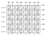
- FIG. 2 is a diagram showing the arrangement of the sensor pixel circuit 9 in the pixel region 4.
- a clock line CLK and one output line OUT are connected to each of the (n ⁇ m / 2) sensor pixel circuits 9.
- the sensor pixel circuits 9 connected to the odd-numbered clock lines CLK1 to CLKn-1 are odd-numbered output lines OUT1 to OUTm ⁇ . 1 is connected.
- the sensor pixel circuit 9 connected to the even-numbered clock lines CLK2 to CLKn is connected to the even-numbered output lines OUT2 to OUTm.
- the gate driver circuit 5 drives the gate lines GL1 to GLx. More specifically, the gate driver circuit 5 sequentially selects one gate line from the gate lines GL1 to GLx based on the control signal CSg, sets a high level potential to the selected gate line, and applies to the remaining gate lines. Apply a low level potential. As a result, the y display pixel circuits 8 connected to the selected gate line are collectively selected.
- the source driver circuit 6 drives the source lines SL1 to SLy. More specifically, the source driver circuit 6 applies potentials corresponding to the video signal VS to the source lines SL1 to SLy based on the control signal CSs. At this time, the source driver circuit 6 may perform line sequential driving or dot sequential driving.
- the potentials applied to the source lines SL1 to SLy are written into y display pixel circuits 8 selected by the gate driver circuit 5. Thus, by writing the potential according to the video signal VS to all the display pixel circuits 8 using the gate driver circuit 5 and the source driver circuit 6, a desired image can be displayed on the display panel 2.
- the sensor row driver circuit 7 drives the clock lines CLK1 to CLKn, the reset lines RST1 to RSTn, the read lines RWS1 to RWSn, and the like. More specifically, the sensor row driver circuit 7 applies a high level potential and a low level potential to the clock lines CLK1 to CLKn at predetermined timing (details will be described later) based on the control signal CSr. In addition, the sensor row driver circuit 7 selects one reset line from the reset lines RST1 to RSTn based on the control signal CSr, sets a high level potential for resetting to the selected reset line, and sets the remaining reset lines to the other reset lines. Apply a low level potential. As a result, the m sensor pixel circuits 9 connected to the reset line to which the high level potential is applied are collectively reset.
- the sensor row driver circuit 7 sequentially selects one readout line from the readout lines RWS1 to RWSn based on the control signal CSr, and applies a high level potential for readout to the selected readout line and the remaining readout lines. A low level potential is applied to.
- the m sensor pixel circuits 9 connected to the selected one readout line can be collectively read out.
- the source driver circuit 6 applies a high level potential to the power supply lines VDD1 to VDDm.
- signals corresponding to the amount of light detected by each sensor pixel circuit 9 (hereinafter referred to as sensor signals) are output from the m sensor pixel circuits 9 in a readable state to the output lines OUT1 to OUTm.
- the output line OUT also serves as the source line SL, and the sensor signal output to the output line OUT is input to the source driver circuit 6.
- the source driver circuit 6 amplifies the sensor signal output from the output line OUT, and outputs the amplified signal to the outside of the display panel 2 as the sensor output Sout.
- the sensor output Sout is appropriately processed as necessary by the signal processing circuit 20 provided outside the display panel 2.
- the number of sensor pixel circuits 9 provided in the pixel region 4 may be arbitrary.
- (n ⁇ m) sensor pixel circuits 9 may be provided in the pixel region 4, or the same number (that is, (x ⁇ y / 3)) sensor pixel circuits 9 as the color pixels in the pixel region 4. May be provided.
- a smaller number of sensor pixel circuits 9 than the color pixels for example, 1 to 1/10 of the color pixels may be provided in the pixel region 4.
- the display device is a display device in which a plurality of photodiodes (photosensors) are arranged in the pixel region 4, and includes a plurality of display pixel circuits 8 and a plurality of sensor pixel circuits 9.
- the display panel 2 and a sensor row driver circuit 7 (drive circuit) that outputs a drive signal such as a clock signal CLK to the sensor pixel circuit 9 are provided.
- the configuration of the sensor pixel circuit 9 and the driving method thereof will be described.
- the same name as the signal line is used to identify the signal on the signal line (for example, the signal on the clock line CLK1 is referred to as a clock signal CLK1).
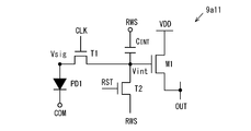
- FIG. 3 is a circuit diagram showing a configuration of a sensor pixel circuit 9 a as a specific example of the sensor pixel circuit 9.
- the sensor pixel circuit 9a is connected to a clock line CLK, a reset line RST, a readout line RWS, a power supply line VDD, and an output line OUT.
- the sensor pixel circuit 9a includes a photodiode PD1, transistors T1, T2, and M1, and a capacitor C INT .
- the transistors T1, T2, M1 are, for example, N-type TFTs (Thin Film Transistors).
- the anode of the photodiode PD1 is connected to the constant voltage source COM.
- the cathode of the photodiode PD1 is connected to the source of the transistor T1.
- the gate of the transistor T1 is connected to the clock line CLK.
- the drain of the transistor T1 is connected to the gate of the transistor M1.
- the drain of the transistor M1 is connected to the power supply line VDD, and the source is connected to the output line OUT.
- the transistor M1 functions as a reading transistor.
- the capacitor C INT is provided between the gate of the transistor M1 and the read line RWS.
- the gate of the transistor T2 is connected to the reset line RST, the drain is connected to the capacitor CINT , and the source is connected to the power supply line REF that supplies the reference voltage Vref.
- the reference voltage Vref is not limited to this, but is 0 V, for example.
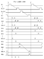
- FIG. 4 is a waveform diagram of a drive signal for driving the sensor pixel circuit 9.
- the potentials of the gate lines GL1 to GLx are set to the high level once every frame period and sequentially for a predetermined time.
- the potentials of the clock lines CLK1 to CLKn become high level for a predetermined time twice in one frame period (time ta, tb).
- the potentials of the reset lines RST1 to RSTn are set to the high level once every frame period (time ta) for a predetermined time (reset period).
- the read lines RWS1 to RWSn are paired in pairs, and the potentials of the (n / 2) pairs of read lines sequentially become high for a predetermined time (read period) after time tc.
- FIG. 5 is a waveform diagram showing changes in various signals of the sensor pixel circuit 9 in the vicinity of the times ta to tc shown in FIG. 6A to 6C are schematic diagrams showing the operation of the sensor pixel circuit 9 when the drive signals shown in FIGS. 4 and 5 are supplied.
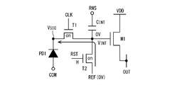
- the transistors T1 and T2 are both turned on as shown in FIG. 6A.
- the potential Vint of the storage node INT becomes substantially equal to the reference voltage Vref (here, 0V).
- the high level potential of the clock signal CLK is set so that the transistor T1 operates in the saturation region.
- the accumulation period starts.
- the clock signal CLK, the reset signal RST, and the read signal RWS are all maintained at a low level.
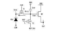
- the transistors T1 and T2 are off.
- the transistors T1 and T2 are off.
- the potential Vint of the accumulation node INT is kept at the potential (Vref) of the reset period.
- Cint is the load capacity of the storage node INT.
- t is the length of the accumulation period (time t2 to t3).
- the clock signal CLK and the reset signal RST are at a low level, and the read signal RWS is at a high level for reading.
- the potential Vint of the storage node INT increases by (Cint / Cp) times the amount of increase in the potential of the read signal RWS (where Cp is the total capacitance value of the sensor pixel circuit 9).
- the transistor M1 forms a source follower amplifier circuit using a transistor (not shown) included in the source driver circuit 6 as a load, and drives the output line OUT according to the potential Vint.
- time t1 in FIG. 5 corresponds to time ta in FIG. 4, and time t3 corresponds to time tb.
- Time t5 corresponds to time tc.
- the sensor pixel circuit 9a is provided with the reset transistor T2, and reset is performed so that the transistor T1 operates in the saturation region in the reset period.
- the transistor T1 since the transistor T1 is provided between the photodiode PD1 and the storage node INT, a relatively large load capacitance of the photodiode PD1 can be separated from the capacitor Cint, and the sensitivity is high. Is obtained.
- the load capacitance of the photodiode PD1 is mainly caused by the capacitance formed between the photodiode PD1 and the light shielding layer provided on the back surface (backlight side).
- the amount of decrease ⁇ Vint of the potential Vint during the accumulation period is Q, where Q is the accumulated charge on the cathode side of the photodiode PD1, and Cpd is the load capacitance of the photodiode PD1.
- ⁇ Vint Q / (Cint + Cpd) (3) It can be expressed as.
- ⁇ Vint is not affected by the load capacitance Cpd of the photodiode PD1. Therefore, according to the sensor pixel circuit 9a, the amount of decrease in ⁇ Vint during the accumulation period increases, and a highly sensitive photosensor can be realized.
- FIG. 7 is a circuit diagram showing a configuration of a sensor pixel circuit 9a1 as a modified example of the sensor pixel circuit 9a according to the first embodiment.
- the sensor pixel circuit 9a1 is formed by forming a capacitor C1 with a transistor TC which is a P-type TFT.
- the drain of the transistor TC is connected to the drain of the transistor T1, the source is connected to the gate of the transistor M1, and the gate is connected to the read line RWS.
- the transistor TC connected in this manner greatly changes the potential of the storage node Vint as compared with the sensor pixel circuit 9a when a high level for reading is applied to the reading line RWS. Therefore, the sensitivity of the sensor pixel circuit can be improved by amplifying the difference between the potential of the storage node Vint when strong light is incident and the potential of the storage node Vint when weak light is incident.
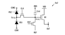
- FIG. 8 is a circuit diagram showing a configuration of a sensor pixel circuit 9a2 as a modification of the sensor pixel circuit 9a according to the first embodiment.
- the sensor pixel circuit 9a2 shown in FIG. 8 is obtained by adding another photodiode PD2 to the sensor pixel circuit 9a.
- the voltage supplied to the anode of the photodiode PD1 is COM1.
- the photodiode PD2 is shielded so that light does not enter, and functions as a reference light sensor.
- the anode of the photodiode PD2 is connected to the cathode of the photodiode PD1 and the source of the transistor T1, and a constant voltage COM2 is applied to the cathode.
- the constant voltage COM1 supplied to the anode of the photodiode PD1 and the constant voltage COM2 supplied to the cathode of the photodiode PD2 are set so as to operate as COM2>Vsig> COM1. According to the configuration of FIG. 8, since a dark current flows through the photodiode PD2, the temperature compensation of the photodiode can be performed.
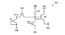
- FIG. 9 is a circuit diagram showing a configuration of a sensor pixel circuit 9a3 as a modification of the sensor pixel circuit 9a according to the first embodiment.
- a sensor pixel circuit 9a3 shown in FIG. 9 is obtained by replacing the photodiode PD1 included in the sensor pixel circuit 9a with a phototransistor TD.
- all the transistors included in the sensor pixel circuit 9a3 can be N-type. Therefore, the sensor pixel circuit can be manufactured using a one-channel process that can manufacture only N-type transistors.
- FIG. 10 is a circuit diagram showing a configuration of a sensor pixel circuit 9a4 as a modified example of the sensor pixel circuit 9a according to the first embodiment.
- the sensor pixel circuit 9a4 according to FIG. 10 is obtained by connecting the photodiode PD1 included in the sensor pixel circuit 9a in reverse.
- the sensor pixel circuit 9a4 is supplied with a reset signal RST which is normally at a high level and becomes a reset low level at the time of reset.
- the cathode of the photodiode PD1 is connected to the constant voltage line COM, and the anode is connected to the source of the transistor T1. Thereby, variations of the pixel circuit can be obtained.
- FIG. 11 is a circuit diagram showing a configuration of a sensor pixel circuit 9a5 as a modification of the sensor pixel circuit 9a according to the first embodiment.
- a sensor pixel circuit 9a5 shown in FIG. 11 is obtained by connecting the photodiode PD1 included in the sensor pixel circuit 9a in reverse, and omitting the capacitor CINT . Further, the readout line RWS is also omitted in the sensor pixel circuit 9a5.
- the sensor pixel circuit 9a5 is supplied with a reset signal RST which is normally at a high level and at a resetting low level at the same time as the sensor pixel circuit 9a4 according to the above-described modification 4.
- the reset signal RST becomes a high level for reading at the time of reading.
- the potential of the storage node Vint (the gate potential of the transistor M1) rises, and a current corresponding to the potential of the storage node Vint flows through the transistor M1.
- the capacitor C INT is omitted from the sensor pixel circuit 9a5, it is possible to increase the aperture ratio by the amount of the capacitor C INT and improve the sensitivity of the sensor pixel circuit.
- FIG. 12 is a circuit diagram showing a configuration of a sensor pixel circuit 9a6 as a modification of the sensor pixel circuit 9a according to the first embodiment.
- the sensor pixel circuit 9a6 shown in FIG. 12 is obtained by omitting the capacitor CINT from the sensor pixel circuit 9a and adding a transistor TS.
- the transistor TS is an N-type TFT and functions as a selection switching element.
- the source of the transistor M1 is connected to the drain of the transistor TS.
- the source of the transistor TS is connected to the output line OUT, and the gate is connected to the readout line RWS.
- variations of the pixel circuit can be obtained.
- the capacitor C INT is omitted, the aperture ratio is increased by the amount of the capacitor C INT , and the sensitivity of the sensor pixel circuit can be improved.
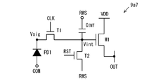
- FIG. 13 is a circuit diagram showing a configuration of a sensor pixel circuit 9a7 as a variation of the sensor pixel circuit 9 according to the first embodiment.
- the sensor pixel circuit 9a7 is different from the sensor pixel circuit 9a in that the source of the transistor T2 is connected to the readout wiring RWS instead of the power supply line REF that supplies the reference voltage Vref. .
- the power line REF for the reference voltage is not necessary, so that there is an advantage that the number of bus lines can be reduced.
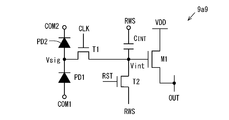
- the source of the transistor T2 is not the power supply line REF that supplies the reference voltage Vref, but the readout wiring RWS.
- Circuit configurations 9a8 to 9a13 corresponding to the configuration connected to the can also be adopted as variations of the sensor pixel circuit 9. These circuit configurations also have an advantage that the number of bus lines can be reduced because the reference voltage power supply line REF is not required, as in the case of the sensor pixel circuit 9a7.
- the specific configuration of the sensor pixel circuit 9 is the same as that of the sensor pixel circuit 9a described in the first embodiment, but the driving method is different.
- FIG. 20 is a waveform diagram showing a drive signal applied to the sensor pixel circuit 9a and potential changes at the node SIG and the storage node INT in the second embodiment. As shown in FIG. 20, in the second embodiment, the clock signal CLK becomes a high level only once in one frame period.
- the clock signal CLK and the reset signal RST are at a high level, and the read signal RWS is at a low level.
- the transistors T1 and T2 are both on.
- the potential Vsig of the node SIG and the potential Vint of the storage node INT are reset to predetermined levels, respectively.
- the potential Vint of the storage node INT is reset to the constant voltage Vref, and the potential Vsig of the node SIG is reset to Vclk ⁇ Vth.
- the potential of Vref is set to a value larger than the potential of Vclk.
- the transistor T1 is set to always operate in the saturation region.
- charge accumulation and charge transfer to the accumulation node INT are performed simultaneously from time t2 to t3. From time t2 to t3, the clock signal CLK is maintained at a high level, and the reset signal RST and the read signal RWS are at a low level, so that the transistor T1 is on and the transistor T2 is off.
- a photocurrent Ipd flows from the node SIG through the photodiode PD1 to the power supply line COM, and charges are extracted from the node SIG.
- the transistor T1 since the transistor T1 is on, the charge extracted by the photocurrent Ipd is replenished from the storage node INT.
- the potential Vint of the storage node INT drops by an amount corresponding to this charge.
- the transistor M1 forms a source follower amplifier circuit using a transistor (not shown) included in the source driver circuit 6 as a load, and outputs according to the potential of the storage node Vint. Drive the line OUT.
- the sensor pixel circuit 9a is provided with the reset transistor T2, and reset is performed so that the transistor T1 operates in the saturation region in the reset period.
- the transistor T1 since the transistor T1 is provided between the photodiode PD1 and the storage node INT, a relatively large load capacitance of the photodiode PD1 can be separated from the capacitor Cint, and the sensitivity is high. Is obtained.
- FIG. 21 is a diagram illustrating an arrangement of the sensor pixel circuit 9 in the pixel region 4 of the display device according to the third embodiment.
- a first sensor pixel circuit 9_on that detects light incident during the lighting period of the backlight 3 and light incident during the extinguishing period of the backlight 3 are detected.
- a second sensor pixel circuit 9_off The number of first sensor pixel circuits 9_on and the number of second sensor pixel circuits 9_off are the same.
- first sensor pixel circuits 9_on are arranged in the vicinity of intersections of odd-numbered clock lines CLK1 to CLKn-1 and odd-numbered output lines OUT1 to OUTm-1.
- the (n ⁇ m / 4) second sensor pixel circuits 9_off are arranged in the vicinity of the intersections of the even-numbered clock lines CLK2 to CLKn and the even-numbered output lines OUT2 to OUTm.
- the display panel 2 includes the plurality of output lines OUT1 to OUTm that propagate the output signal of the first sensor pixel circuit 9_on and the output signal of the second sensor pixel circuit 9_off, and includes the first sensor pixel circuit 9_on and the second sensor.
- the pixel circuit 9_off is connected to different output lines.
- the source driver circuit 6 includes a difference circuit (not shown) for obtaining a difference between the output signal of the first sensor pixel circuit 9_on and the output signal of the second sensor pixel circuit 9_off.
- the source driver circuit 6 amplifies the light amount difference obtained by the difference circuit, and outputs the amplified signal to the outside of the display panel 2 as the sensor output Sout.
- the sensor output Sout is appropriately processed as necessary by the signal processing circuit 20 provided outside the display panel 2.
- FIG. 22 is a diagram showing lighting and extinguishing timings of the backlight 3, and resetting and reading timings for the sensor pixel circuit 9.
- the backlight 3 is lit for a predetermined time once in one frame period, and is turned off in other periods. Specifically, the backlight 3 is turned on at time tA within one frame period, and is turned off at time tB. Further, all the first sensor pixel circuits 9_on are reset at time tA, and all the second sensor pixel circuits 9_off are reset at time tB.
- the first sensor pixel circuit 9_on detects light incident during a period A1 (lighting period of the backlight 3) from time tA to time tB.
- the second sensor pixel circuit 9_off detects light incident during the period A2 (the backlight 3 is turned off) from time tB to time tC.
- the period A1 and the period A2 have the same length. Reading from the first sensor pixel circuit 9_on and reading from the second sensor pixel circuit 9_off are performed in line-sequentially in parallel after time tC. In FIG. 22, the reading from the sensor pixel circuit 9 is completed within one frame period, but it may be completed until the first sensor pixel circuit 9_on is reset in the next frame period.
- FIG. 22 shows an example in which reading from the sensor pixel circuit 9 is performed once in one frame period. However, reading from the sensor pixel circuit 9 may be performed twice or more in one frame period. good.
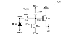
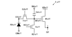
- FIG. 23A and FIG. 23B are circuit diagrams showing examples of specific configurations of the first sensor pixel circuit 9_on and the second sensor pixel circuit 9_off. As shown in FIGS. 23A and 23B, each of the first pixel circuit 9_on and the second pixel circuit 9_off has the same circuit configuration as the sensor pixel circuit 9a described in the first embodiment.
- FIG. 24 is a signal waveform diagram of the display panel 2 according to the present embodiment.
- the potentials of the gate lines GL1 to GLx are set to a high level for a predetermined time in order once every frame period.
- the potentials of the odd-numbered clock lines CLK1 to CLKn ⁇ 1 are set to a high level twice in one frame period and for a predetermined time in the period A1, respectively.
- the potentials of the even-numbered clock lines CLK2 to CLKn are set to the high level twice in one frame period and for a predetermined time in the period A2.
- the potentials of the odd-numbered reset lines RST1 to RSTn ⁇ 1 are set to the high level once every frame period and for a predetermined time at the beginning of the period A1.
- the potentials of the even-numbered reset lines RST2 to RSTn are set to the high level once every frame period and for a predetermined time at the beginning of the period A2.
- the read lines RWS1 to RWSn are paired in pairs, and the potentials of the (n / 2) pairs of read lines sequentially become high for a predetermined time after time tC.
- Vint_on Vref ⁇ Ipd_on ⁇ t / Cint ... (5) It becomes.
- Ipd_on represents the current value of the photocurrent that has flowed through the photodiode PD1 during the accumulation period (accumulation period within the period A1) in a state where the backlight 3 is turned on.
- Vint_off Vref ⁇ Ipd_off ⁇ t / Cint ... (6) It becomes.
- Ipd_off represents the current value of the current that has flowed through the photodiode PD1 during the accumulation period (accumulation period within the period A2) when the backlight 3 is turned off.
- the first sensor pixel circuit 9_on and the second sensor pixel circuit 9_off according to the amount of light incident on the detection period when the backlight 3 is turned on, as described above.
- the sensor signal and the sensor signal corresponding to the amount of light incident during the detection period when the backlight 3 is turned off are read out.
- the difference circuit included in the source driver circuit 6 obtains the difference between the output signal of the first sensor pixel circuit 9_on and the output signal of the second sensor pixel circuit 9_off, so that the amount of light when the backlight is turned on and the time when the backlight is turned off are calculated. The difference in the amount of light can be obtained.
- the output signal from the second sensor pixel circuit 9_off that is, the sensor signal corresponding to the amount of light incident during the detection period when the backlight 3 is turned off contains only noise components caused by the surrounding environment. Therefore, in the difference circuit of the source driver circuit 6, by subtracting the output signal from the second sensor pixel circuit 9_off from the output signal from the first sensor pixel circuit 9_on, a highly accurate sensor output from which noise components have been removed is obtained. Obtainable.
- the potential drop amount ⁇ Vint of the storage node during the storage period is the load capacitance of the photodiode PD1. Not affected by Cpd. Therefore, a highly sensitive photosensor can also be realized by this embodiment.
- the circuit configuration of the first sensor pixel circuit 9_on and the second sensor pixel circuit 9_0ff is not the sensor pixel circuit 9a but the first embodiment.
- the sensor pixel circuits 9a1 to 9a13 described in the embodiments may be adopted, and the same effects as described above can be obtained.
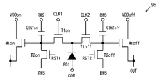
- FIG. 25 is a circuit diagram of a sensor pixel circuit 9c according to the third embodiment.
- a sensor pixel circuit 9c shown in FIG. 25 includes transistors T1on, T1off, T2on, T2off, M1on, M1off, a photodiode PD1, and capacitors Cinton, Cinoff.
- the transistors T1on, T1off, T2on, T2off, M1on, and M1off are N-type TFTs.
- the photodiode PD1 and the left half circuit element correspond to a first sensor pixel circuit that obtains a sensor output based on an accumulation period when the backlight 3 is lit.
- Half of the circuit elements correspond to a second sensor pixel circuit that obtains a sensor output based on an accumulation period when the backlight 3 is turned off. That is, the sensor pixel circuit 9c also functions as the sensor pixel circuit 9_on and the sensor pixel circuit 9_off described above.
- the sensor pixel circuit 9c is connected to clock lines CLKon and CLKoff, reset lines RSTon and RSToff, readout line RWS, power supply lines VDDon and VDDoff, and output lines OUTon and OUToff.
- the anode of the photodiode PD1 is connected to the constant voltage source COM, and the cathode is connected to the sources of the transistors T1on and T1off.
- the gate of the transistor T1on is connected to the clock line CLK1, and the drain is connected to the gate of the transistor M1on.
- the drain of the transistor M1on is connected to the power supply line VDDon, and the source is connected to the output line OUTon.
- the capacitor C1on is provided between the gate of the transistor M1on and the read line RWS.
- the gate of the transistor T1off is connected to the clock line CLK2, and the drain is connected to the gate of the transistor M1off.
- the drain of the transistor M1off is connected to the power supply line VDDoff, and the source is connected to the output line OUToff.
- the capacitor CINToff is provided between the gate of the transistor M1off and the readout line RWS.
- a node connected to the gate of the transistor M1on is a first storage node
- a node connected to the gate of the transistor M1off is a second storage node
- the transistors M1on and M1off function as readout transistors.
- the sensor pixel circuit 9c is driven by the drive signal shown in FIG. 24, and, similarly to the third embodiment, the output signal from the output line OUToff is subtracted from the output signal from the output line OUTon.
- a highly accurate sensor output from which noise components are removed can be obtained.
- the potential drop amount ⁇ Vint of the storage node during the storage period is affected by the load capacitance Cpd of the photodiode PD1. I do not receive it. Therefore, a highly sensitive photosensor can also be realized by this embodiment.
- the sensor pixel circuit 9c shown in FIG. 25 is applied to the sensor pixel circuit 9a in the first embodiment in order to obtain sensor pixel circuits 9a1 to 9a6 as modifications of the first embodiment. It is also possible to apply the same modification. Hereinafter, these modified examples will be described.
- FIG. 26 is a circuit diagram showing a configuration of a sensor pixel circuit 9c1 as a modified example of the sensor pixel circuit 9c.
- a sensor pixel circuit 9c1 shown in FIG. 26 is obtained by forming the capacitor C INT of the sensor pixel circuit 9c with a transistor TC which is a P-type TFT.
- the drain of the transistor TC is connected to the drain of the transistor T1, the source is connected to the gate of the transistor M1, and the gate is connected to the read line RWS.
- the transistor TC connected in this manner greatly changes the potential of the storage node Vint as compared with the sensor pixel circuit 9a when a high level for reading is applied to the reading line RWS. Therefore, the sensitivity of the sensor pixel circuit can be improved by amplifying the difference between the potential of the storage node Vint when strong light is incident and the potential of the storage node Vint when weak light is incident.
- FIG. 27 is a circuit diagram showing a configuration of a sensor pixel circuit 9c2 as a modified example of the sensor pixel circuit 9c.
- a sensor pixel circuit 9c2 shown in FIG. 27 is obtained by adding another photodiode PD2 to the sensor pixel circuit 9c.
- the photodiode PD2 is shielded so that light does not enter, and functions as a reference light sensor.
- the anode of the photodiode PD2 is connected to the cathode of the photodiode PD1 and the sources of the transistors T1on and T1off.
- a constant voltage COM2 is applied to the cathode. Since dark current flows through the photodiode PD2, temperature compensation of the photodiode can be performed.
- FIG. 27 is a circuit diagram showing a configuration of a sensor pixel circuit 9c2 as a modified example of the sensor pixel circuit 9c.
- a sensor pixel circuit 9c2 shown in FIG. 27 is obtained by adding
- the constant voltage COM supplied to the anode of the photodiode PD1 and the constant voltage COM2 supplied to the cathode of the photodiode PD2 are COM2> (potential between the diodes PD1 and PD2)> COM It is set so that
- FIG. 28 is a circuit diagram showing a configuration of a sensor pixel circuit 9c3 as a modified example of the sensor pixel circuit 9c.
- a sensor pixel circuit 9c3 shown in FIG. 28 is obtained by replacing the photodiode PD1 included in the sensor pixel circuit 9c with a phototransistor TD.
- all the transistors included in the sensor pixel circuit 9c3 can be N-type. Therefore, the sensor pixel circuit can be manufactured using a one-channel process that can manufacture only N-type transistors.
- FIG. 29 is a circuit diagram showing a configuration of a sensor pixel circuit 9c4 as a modified example of the sensor pixel circuit 9c.
- the sensor pixel circuit 9c4 according to FIG. 29 is obtained by connecting the photodiode PD1 included in the sensor pixel circuit 9c in reverse.
- the sensor pixel circuit 9c4 is supplied with a reset signal RST which is normally at a high level and becomes a reset low level at the time of reset.
- the cathode of the photodiode PD1 is connected to the constant voltage line COM, and the anode is connected to the sources of the transistors T1on and T1off. Thereby, variations of the pixel circuit can be obtained.
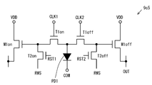
- FIG. 30 is a circuit diagram showing a configuration of a sensor pixel circuit 9c5 as a modification of the sensor pixel circuit 9c.
- a sensor pixel circuit 9c5 shown in FIG. 30 is obtained by connecting the photodiode PD1 included in the sensor pixel circuit 9c in reverse, and omitting the capacitor CINT .
- the sensor pixel circuit 9c5 is supplied with a reset signal RST that is normally at a high level and at a resetting low level. However, the reset signal RST becomes a high level for reading at the time of reading.
- the potential of the storage node Vint (the gate potential of the transistor M1) rises, and a current corresponding to the potential of the storage node Vint flows through the transistor M1.
- the capacitor C INT is omitted from the sensor pixel circuit 9c5
- the aperture ratio is increased by the amount of the capacitor C INT , and the sensitivity of the sensor pixel circuit can be improved.
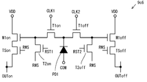
- FIG. 31 is a circuit diagram showing a configuration of a sensor pixel circuit 9c6 as a modified example of the sensor pixel circuit 9c.
- a sensor pixel circuit 9c6 shown in FIG. 31 is obtained by omitting the capacitor CINT from the sensor pixel circuit 9c and adding transistors Tson and TSoff.
- the transistors Tson and TSoff are N-type TFTs and function as selection switching elements.
- the sources of the transistors M1on and M1off are connected to the drains of the transistors TSon and TSoff, respectively.
- the sources of the transistors TSon and TSoff are connected to the output lines OUTon and OUToff, respectively, and the gates are connected to the read line RWS.
- variations of the pixel circuit can be obtained.
- the capacitor C INT is omitted, the aperture ratio is increased by the amount of the capacitor C INT , and the sensitivity of the sensor pixel circuit can be improved.
- the sensor pixel circuit 9c and the sensor pixel circuits 9c1 to 9c6 include the first sensor pixel circuit for obtaining the sensor output according to the accumulation period when the backlight 3 is turned on, and the backlight 3 being turned off.
- the second sensor pixel circuit for obtaining the sensor output according to the accumulation period of time has a configuration sharing one photodiode PD1 (light receiving element).
- the cathode of the shared photodiode PD1 is connected to the source of the transistor T1on included in the portion corresponding to the first pixel circuit and the source of the transistor T1off included in the portion corresponding to the second pixel circuit.
- the sensor pixel circuit 9c can detect the amount of light when the backlight is turned on and the amount of light when the backlight is turned off. Further, one photo pixel circuit between the first sensor pixel circuit for obtaining the sensor output based on the accumulation period when the backlight 3 is turned on and the second sensor pixel circuit for obtaining the sensor output based on the accumulation period when the backlight 3 is turned off. By sharing the diode PD1, the influence of variations in the sensitivity characteristics of the photodiode is canceled. Thereby, the difference between the light amount when the backlight is turned on and the light amount when the backlight is turned off can be accurately obtained. In addition, the number of photodiodes can be reduced, the aperture ratio can be increased, and the sensitivity of the sensor pixel circuit can be increased.
- the display device includes, as the sensor pixel circuit 9, the first sensor pixel circuit 9_on and the second sensor pixel circuit 9_off illustrated in FIGS. 23A and 23B in the third embodiment. .
- the lighting / extinguishing timing of the backlight 3 is also the same as that of the third embodiment (see FIG. 22).
- FIG. 32 is a signal waveform diagram of the display panel 2 according to the present embodiment.
- the timing of the clock signal CLK is different from that of the third embodiment.
- the potentials of the odd-numbered clock lines CLK1 to CLKn-1 are set to the high level once every frame period and for a predetermined time in the period A1.
- the potentials of the even-numbered clock lines CLK2 to CLKn are set to the high level once every frame period and for a predetermined time in the period A2.
- the timings of the reset signal RST and the read signal RWS are the same as in the third embodiment.
- a sensor signal corresponding to the amount and a sensor signal corresponding to the amount of light incident during the detection period when the backlight 3 is turned off are read out.
- the difference circuit included in the source driver circuit 6 obtains the difference between the output signal of the first sensor pixel circuit 9_on and the output signal of the second sensor pixel circuit 9_off, so that the amount of light when the backlight is turned on and the time when the backlight is turned off are calculated. The difference in the amount of light can be obtained.
- the output signal from the second sensor pixel circuit 9_off that is, the sensor signal corresponding to the amount of light incident during the detection period when the backlight 3 is turned off contains only noise components caused by the surrounding environment. Therefore, in the difference circuit of the source driver circuit 6, by subtracting the output signal from the second sensor pixel circuit 9_off from the output signal from the first sensor pixel circuit 9_on, a highly accurate sensor output from which noise components have been removed is obtained. Obtainable.
- the potential drop amount ⁇ Vint of the storage node during the storage period is a photo It is not affected by the load capacitance Cpd of the diode PD1. Therefore, a highly sensitive photosensor can also be realized by this embodiment.
- the fourth embodiment has been described above.
- the circuit configuration of the first sensor pixel circuit 9_on and the second sensor pixel circuit 9_off is not the sensor pixel circuit 9a but the first embodiment.
- the sensor pixel circuits 9a1 to 9a13 described in the embodiments may be adopted, and the same effects as described above can be obtained.
- the sensor pixel circuit 9c described in the third embodiment may be employed, and the same effects as described above are achieved. Furthermore, sensor pixel circuits 9c1 to 9c6 as modifications of the sensor pixel circuit 9c may be employed.
- the driving method for acquiring the off signal first and then acquiring the on signal in one frame period has been described.
- the present invention is industrially applicable as a display device having an optical sensor function.
Landscapes
- Engineering & Computer Science (AREA)
- Theoretical Computer Science (AREA)
- General Engineering & Computer Science (AREA)
- Physics & Mathematics (AREA)
- General Physics & Mathematics (AREA)
- Human Computer Interaction (AREA)
- Computer Networks & Wireless Communication (AREA)
- Computer Hardware Design (AREA)
- Liquid Crystal (AREA)
- Control Of Indicators Other Than Cathode Ray Tubes (AREA)
- Liquid Crystal Display Device Control (AREA)
Abstract
感度が向上された光センサ付きの表示装置を提供する。表示装置は、複数の表示画素回路(8)および複数のセンサ画素回路(9a)を表示領域(4)内に含む表示パネルと、前記センサ画素回路(9a)に対して駆動信号を供給する駆動回路(7)とを備える。前記センサ画素回路(9a)は、受光素子(PD1)と、前記受光素子(PD1)へ入射した光量に応じた電荷を保持する蓄積ノード(INT)と、前記蓄積ノード(INT)に接続された読み出しスイッチング素子(M1)とを備える。前記表示装置は、前記受光素子(PD1)と前記蓄積ノード(INT)との間に接続され、飽和領域で動作する第1のスイッチング素子(T1)と、前記蓄積ノード(INT)をリセットする第2のスイッチング素子(T2)とをさらに備える。
Description
本発明は、表示装置に関し、特に、画素領域に複数の光センサを配置した表示装置に関する。
従来から表示装置に関し、表示パネルに複数の光センサを設け、タッチパネル、ペン入力、スキャナなどの入力機能を提供する方法が知られている。このような光センサの一例として、図33に示すように、フォトダイオードPD1と、コンデンサCINTと、トランジスタM1とを備えた回路構成が知られている(国際公開第2007/145346号および国際公開第2007/145347号を参照)。
この従来の光センサにおいて、トランジスタM1のゲートは、蓄積ノードINTに接続されている。蓄積ノードINTは、コンデンサCINTの一方の電極と、フォトダイオードPD1の一方の電極(カソード)とに接続されている。フォトダイオードPD1の他方の電極(アノード)は、リセット線RSTに接続されている。コンデンサCINTの他方の電極は、読み出し配線RWSに接続されている。
上記従来の光センサの動作は次のとおりである。まず、リセット期間において、リセット線RSTに、フォトダイオードPD1に順方向バイアスをかける電圧を供給する。これにより、リセット期間において、蓄積ノードINTは所定電位にリセットされる。リセット期間が終了すると、リセット線RSTには、フォトダイオードPD1に逆方向バイアスをかける電圧が供給される。リセット期間に続く蓄積期間においては、蓄積ノードINTへの電荷蓄積が行われる。蓄積期間に続く読み出し期間において、読み出し配線RWSに読み出し電圧を印加することにより、蓄積期間に蓄積された電荷が、蓄積ノードINTからトランジスタM1によって読み出される。
上記従来の光センサにおいて、感度を向上させるためには、CINTの容量を小さくするか、フォトダイオードPD1のサイズまたは数を大きくする必要がある。しかし、フォトダイオードPD1のサイズまたは数を大きくすると、その負荷容量も増加するので、結果として、感度向上の効果を得ることが難しいという問題があった。本発明は、上記の問題を解決し、感度が向上された光センサ付きの表示装置を提供することを目的とする。
上記の目的を達成するために、ここに開示する表示装置は、複数の表示画素回路および複数のセンサ画素回路を表示領域内に含む表示パネルと、前記センサ画素回路に対して駆動信号を供給する駆動回路とを備え、前記センサ画素回路は、受光素子と、前記受光素子へ入射した光量に応じた電荷を保持する蓄積ノードと、前記蓄積ノードに接続された読み出しスイッチング素子とを備え、前記受光素子と前記蓄積ノードとの間に接続され、飽和領域で動作する第1のスイッチング素子と、前記蓄積ノードをリセットする第2のスイッチング素子とをさらに備えた構成である。
本発明によれば、感度が向上された光センサ付きの表示装置を提供できる。
本発明の一実施形態にかかる表示装置は、
複数の表示画素回路および複数のセンサ画素回路を表示領域内に含む表示パネルと、
前記センサ画素回路に対して駆動信号を供給する駆動回路とを備え、
前記センサ画素回路は、
受光素子と、
前記受光素子へ入射した光量に応じた電荷を蓄積する第1の蓄積ノードと、
前記第1の蓄積ノードの電荷を保持するための第2の蓄積ノードと、
前記第2の蓄積ノードに接続された読み出しスイッチング素子とを備え、
前記第1の蓄積ノードと前記第2の蓄積ノードとの間に接続され、前記第1の蓄積ノードで蓄積した電荷を前記第2の蓄積ノードに転送するとき、飽和領域で動作する第1のスイッチング素子と、
前記第2の蓄積ノードに接続され、前記第1および第2の蓄積ノードをリセットする第2のスイッチング素子とをさらに備えた構成である(第1の構成)。
複数の表示画素回路および複数のセンサ画素回路を表示領域内に含む表示パネルと、
前記センサ画素回路に対して駆動信号を供給する駆動回路とを備え、
前記センサ画素回路は、
受光素子と、
前記受光素子へ入射した光量に応じた電荷を蓄積する第1の蓄積ノードと、
前記第1の蓄積ノードの電荷を保持するための第2の蓄積ノードと、
前記第2の蓄積ノードに接続された読み出しスイッチング素子とを備え、
前記第1の蓄積ノードと前記第2の蓄積ノードとの間に接続され、前記第1の蓄積ノードで蓄積した電荷を前記第2の蓄積ノードに転送するとき、飽和領域で動作する第1のスイッチング素子と、
前記第2の蓄積ノードに接続され、前記第1および第2の蓄積ノードをリセットする第2のスイッチング素子とをさらに備えた構成である(第1の構成)。
前記第1の構成において、
前記センサ画素回路が、
前記第2の蓄積ノードと読み出し信号線との間に接続されたコンデンサをさらに備え、
前記第2のスイッチング素子のゲートにリセット線が接続され、ソースに定電圧源が接続され、ドレインに前記第2の蓄積ノードが接続された構成としても良い(第2の構成)。
前記センサ画素回路が、
前記第2の蓄積ノードと読み出し信号線との間に接続されたコンデンサをさらに備え、
前記第2のスイッチング素子のゲートにリセット線が接続され、ソースに定電圧源が接続され、ドレインに前記第2の蓄積ノードが接続された構成としても良い(第2の構成)。
あるいは、前記第1の構成において、
前記センサ画素回路が、
前記第2の蓄積ノードと読み出し信号線との間に接続されたコンデンサをさらに備え、
前記第2のスイッチング素子のゲートにリセット線が接続され、ソースに前記読み出し信号線が接続され、ドレインに前記第2の蓄積ノードが接続された構成としても良い(第3の構成)。
前記センサ画素回路が、
前記第2の蓄積ノードと読み出し信号線との間に接続されたコンデンサをさらに備え、
前記第2のスイッチング素子のゲートにリセット線が接続され、ソースに前記読み出し信号線が接続され、ドレインに前記第2の蓄積ノードが接続された構成としても良い(第3の構成)。
前記第1~第3の構成において、
前記駆動回路が、単位期間内に、
前記第1のスイッチング素子をオンにすると共に前記第2のスイッチング素子をオンして、前記第1および第2の蓄積ノードをリセットするリセット期間と、
前記第1のスイッチング素子をオフにすると共に前記第2のスイッチング素子をオフして、前記第1の蓄積ノードにおいて前記受光素子で受光された光量に応じた電荷を蓄積する蓄積期間と、
前記第1のスイッチング素子をオンにすると共に前記第2のスイッチング素子をオフして、前記第1の蓄積ノードにおいて前記蓄積期間に蓄積した電荷を前記第2の蓄積ノードへ転送する転送期間と、
前記第1のスイッチング素子をオフにすると共に前記第2のスイッチング素子をオフして、前記読み出しスイッチング素子をオンにして読み出しを行う読み出し期間とによってセンシングを行う構成とすることが好ましい(第4の構成)。
前記駆動回路が、単位期間内に、
前記第1のスイッチング素子をオンにすると共に前記第2のスイッチング素子をオンして、前記第1および第2の蓄積ノードをリセットするリセット期間と、
前記第1のスイッチング素子をオフにすると共に前記第2のスイッチング素子をオフして、前記第1の蓄積ノードにおいて前記受光素子で受光された光量に応じた電荷を蓄積する蓄積期間と、
前記第1のスイッチング素子をオンにすると共に前記第2のスイッチング素子をオフして、前記第1の蓄積ノードにおいて前記蓄積期間に蓄積した電荷を前記第2の蓄積ノードへ転送する転送期間と、
前記第1のスイッチング素子をオフにすると共に前記第2のスイッチング素子をオフして、前記読み出しスイッチング素子をオンにして読み出しを行う読み出し期間とによってセンシングを行う構成とすることが好ましい(第4の構成)。
あるいは、前記第1~第3の構成において、
前記駆動回路が、単位期間内に、
前記第1のスイッチング素子をオンにすると共に前記第2のスイッチング素子をオンして、前記第1および第2の蓄積ノードをリセットするリセット期間と、
前記第1のスイッチング素子をオンにすると共に前記第2のスイッチング素子をオフして、前記第1の蓄積ノードにおいて前記受光素子で受光された光量に応じた電荷を蓄積すると同時に、前記第1の蓄積ノードにおいて前記蓄積期間に蓄積した電荷を前記第2の蓄積ノードへ転送する蓄積転送期間と、
前記第1のスイッチング素子をオフにすると共に前記第2のスイッチング素子をオフして、前記読み出しスイッチング素子をオンにして読み出しを行う読み出し期間とによってセンシングを行う構成とすることも好ましい(第5の構成)。
前記駆動回路が、単位期間内に、
前記第1のスイッチング素子をオンにすると共に前記第2のスイッチング素子をオンして、前記第1および第2の蓄積ノードをリセットするリセット期間と、
前記第1のスイッチング素子をオンにすると共に前記第2のスイッチング素子をオフして、前記第1の蓄積ノードにおいて前記受光素子で受光された光量に応じた電荷を蓄積すると同時に、前記第1の蓄積ノードにおいて前記蓄積期間に蓄積した電荷を前記第2の蓄積ノードへ転送する蓄積転送期間と、
前記第1のスイッチング素子をオフにすると共に前記第2のスイッチング素子をオフして、前記読み出しスイッチング素子をオンにして読み出しを行う読み出し期間とによってセンシングを行う構成とすることも好ましい(第5の構成)。
また、前記第1~第5の構成において、
1フレーム期間に所定時間だけ点灯する光源をさらに含み、
前記センサ画素回路が、光源点灯時の検知期間で光を検知する第1センサ画素回路と、光源消灯時の検知期間で光を検知する第2センサ画素回路とを含み、
前記駆動回路が、光源点灯時の検知期間および光源消灯時の検知期間以外において、前記第1および第2センサ画素回路からの読み出しを線順次で行う構成とすることも好ましい(第6の構成)。
1フレーム期間に所定時間だけ点灯する光源をさらに含み、
前記センサ画素回路が、光源点灯時の検知期間で光を検知する第1センサ画素回路と、光源消灯時の検知期間で光を検知する第2センサ画素回路とを含み、
前記駆動回路が、光源点灯時の検知期間および光源消灯時の検知期間以外において、前記第1および第2センサ画素回路からの読み出しを線順次で行う構成とすることも好ましい(第6の構成)。
前記第6の構成において、
前記光源は1フレーム期間に1回所定時間だけ点灯し、
光源点灯時の検知期間および光源消灯時の検知期間は、1フレーム期間に1回ずつ設定されている構成とすることがさらに好ましい(第7の構成)。
前記光源は1フレーム期間に1回所定時間だけ点灯し、
光源点灯時の検知期間および光源消灯時の検知期間は、1フレーム期間に1回ずつ設定されている構成とすることがさらに好ましい(第7の構成)。
前記第6または第7の構成において、
前記第1センサ画素回路と第2センサ画素回路とが、1個の光センサを共有している構成とすることが好ましい(第8の構成)。
前記第1センサ画素回路と第2センサ画素回路とが、1個の光センサを共有している構成とすることが好ましい(第8の構成)。
前記第1~第8の構成において、
前記第1のコンデンサがP型トランジスタである構成とすることが好ましい(第9の構成)。
前記第1のコンデンサがP型トランジスタである構成とすることが好ましい(第9の構成)。
前記第1~第8の構成において、
前記センサ画素回路が、
前記受光素子に直列に接続され、遮光された参照用受光素子をさらに含み、
前記受光素子と前記参照用受光素子との間に、前記第1の蓄積ノードが接続されている構成とすることが好ましい(第10の構成)。
前記センサ画素回路が、
前記受光素子に直列に接続され、遮光された参照用受光素子をさらに含み、
前記受光素子と前記参照用受光素子との間に、前記第1の蓄積ノードが接続されている構成とすることが好ましい(第10の構成)。
前記第1~第8の構成において、
前記受光素子がN型トランジスタである構成としても良い(第11の構成)。
前記受光素子がN型トランジスタである構成としても良い(第11の構成)。
前記第1~第8の構成において、
前記読み出しスイッチング素子に直列に接続され、前記第2の蓄積ノードと当該センサ画素回路の出力線との導通/非導通を制御する選択スイッチング素子をさらに備えた構成とすることが好ましい。
前記読み出しスイッチング素子に直列に接続され、前記第2の蓄積ノードと当該センサ画素回路の出力線との導通/非導通を制御する選択スイッチング素子をさらに備えた構成とすることが好ましい。
また、本発明の一実施形態にかかる、表示装置の駆動方法は、
複数の表示画素回路および複数のセンサ画素回路を表示領域内に含む表示パネルと、前記センサ画素回路に対して駆動信号を供給する駆動回路とを備え、前記センサ画素回路が、受光素子と、前記受光素子へ入射した光量に応じた電荷を蓄積する第1の蓄積ノードと、前記第1の蓄積ノードの電荷を保持するための第2の蓄積ノードと、前記第2の蓄積ノードに接続された読み出しスイッチング素子とを備え、前記第1の蓄積ノードと前記第2の蓄積ノードとの間に接続され、前記第1の蓄積ノードで蓄積した電荷を前記第2の蓄積ノードに転送するとき、飽和領域で動作する第1のスイッチング素子と、前記第2の蓄積ノードに接続され、前記第1および第2の蓄積ノードをリセットする第2のスイッチング素子とをさらに備えた表示装置の駆動方法であって、
前記駆動回路が、単位期間内に、
前記第1のスイッチング素子をオンにすると共に前記第2のスイッチング素子をオンして、前記第1および第2の蓄積ノードをリセットするリセット処理と、
前記第1のスイッチング素子をオフにすると共に前記第2のスイッチング素子をオフして、前記第1の蓄積ノードにおいて前記受光素子で受光された光量に応じた電荷を蓄積する蓄積処理と、
前記第1のスイッチング素子をオンにすると共に前記第2のスイッチング素子をオフして、前記第1の蓄積ノードにおいて前記蓄積処理で蓄積した電荷を前記第2の蓄積ノードへ転送する転送処理と、
前記第1のスイッチング素子をオフにすると共に前記第2のスイッチング素子をオフして、前記読み出しスイッチング素子をオンにして読み出しを行う読み出し処理とによってセンシングを行う方法である。
複数の表示画素回路および複数のセンサ画素回路を表示領域内に含む表示パネルと、前記センサ画素回路に対して駆動信号を供給する駆動回路とを備え、前記センサ画素回路が、受光素子と、前記受光素子へ入射した光量に応じた電荷を蓄積する第1の蓄積ノードと、前記第1の蓄積ノードの電荷を保持するための第2の蓄積ノードと、前記第2の蓄積ノードに接続された読み出しスイッチング素子とを備え、前記第1の蓄積ノードと前記第2の蓄積ノードとの間に接続され、前記第1の蓄積ノードで蓄積した電荷を前記第2の蓄積ノードに転送するとき、飽和領域で動作する第1のスイッチング素子と、前記第2の蓄積ノードに接続され、前記第1および第2の蓄積ノードをリセットする第2のスイッチング素子とをさらに備えた表示装置の駆動方法であって、
前記駆動回路が、単位期間内に、
前記第1のスイッチング素子をオンにすると共に前記第2のスイッチング素子をオンして、前記第1および第2の蓄積ノードをリセットするリセット処理と、
前記第1のスイッチング素子をオフにすると共に前記第2のスイッチング素子をオフして、前記第1の蓄積ノードにおいて前記受光素子で受光された光量に応じた電荷を蓄積する蓄積処理と、
前記第1のスイッチング素子をオンにすると共に前記第2のスイッチング素子をオフして、前記第1の蓄積ノードにおいて前記蓄積処理で蓄積した電荷を前記第2の蓄積ノードへ転送する転送処理と、
前記第1のスイッチング素子をオフにすると共に前記第2のスイッチング素子をオフして、前記読み出しスイッチング素子をオンにして読み出しを行う読み出し処理とによってセンシングを行う方法である。
また、本発明の他の実施形態にかかる、表示装置の駆動方法は、
複数の表示画素回路および複数のセンサ画素回路を表示領域内に含む表示パネルと、前記センサ画素回路に対して駆動信号を供給する駆動回路とを備え、前記センサ画素回路が、受光素子と、前記受光素子へ入射した光量に応じた電荷を蓄積する第1の蓄積ノードと、前記第1の蓄積ノードの電荷を保持するための第2の蓄積ノードと、前記第2の蓄積ノードに接続された読み出しスイッチング素子とを備え、前記第1の蓄積ノードと前記第2の蓄積ノードとの間に接続され、前記第1の蓄積ノードで蓄積した電荷を前記第2の蓄積ノードに転送するとき、飽和領域で動作する第1のスイッチング素子と、前記第2の蓄積ノードに接続され、前記第1および第2の蓄積ノードをリセットする第2のスイッチング素子とをさらに備えた表示装置の駆動方法であって、
前記駆動回路が、単位期間内に、
前記第1のスイッチング素子をオンにすると共に前記第2のスイッチング素子をオンして、前記第1および第2の蓄積ノードをリセットするリセット処理と、
前記第1のスイッチング素子をオンにすると共に前記第2のスイッチング素子をオフして、前記第1の蓄積ノードにおいて前記受光素子で受光された光量に応じた電荷を蓄積すると同時に、前記第1の蓄積ノードにおいて前記蓄積期間に蓄積した電荷を前記第2の蓄積ノードへ転送する蓄積転送処理と、
前記第1のスイッチング素子をオフにすると共に前記第2のスイッチング素子をオフして、前記読み出しスイッチング素子をオンにして読み出しを行う読み出し処理とによってセンシングを行う方法である。
複数の表示画素回路および複数のセンサ画素回路を表示領域内に含む表示パネルと、前記センサ画素回路に対して駆動信号を供給する駆動回路とを備え、前記センサ画素回路が、受光素子と、前記受光素子へ入射した光量に応じた電荷を蓄積する第1の蓄積ノードと、前記第1の蓄積ノードの電荷を保持するための第2の蓄積ノードと、前記第2の蓄積ノードに接続された読み出しスイッチング素子とを備え、前記第1の蓄積ノードと前記第2の蓄積ノードとの間に接続され、前記第1の蓄積ノードで蓄積した電荷を前記第2の蓄積ノードに転送するとき、飽和領域で動作する第1のスイッチング素子と、前記第2の蓄積ノードに接続され、前記第1および第2の蓄積ノードをリセットする第2のスイッチング素子とをさらに備えた表示装置の駆動方法であって、
前記駆動回路が、単位期間内に、
前記第1のスイッチング素子をオンにすると共に前記第2のスイッチング素子をオンして、前記第1および第2の蓄積ノードをリセットするリセット処理と、
前記第1のスイッチング素子をオンにすると共に前記第2のスイッチング素子をオフして、前記第1の蓄積ノードにおいて前記受光素子で受光された光量に応じた電荷を蓄積すると同時に、前記第1の蓄積ノードにおいて前記蓄積期間に蓄積した電荷を前記第2の蓄積ノードへ転送する蓄積転送処理と、
前記第1のスイッチング素子をオフにすると共に前記第2のスイッチング素子をオフして、前記読み出しスイッチング素子をオンにして読み出しを行う読み出し処理とによってセンシングを行う方法である。
[実施の形態]
以下、本発明のより具体的な実施形態について、図面を参照しながら説明する。なお、以下の実施形態は、本発明にかかる表示装置を液晶表示装置として実施する場合の構成例を示したものであるが、本発明にかかる表示装置は液晶表示装置に限定されず、アクティブマトリクス基板を用いる任意の表示装置に適用可能である。なお、本発明にかかる表示装置は、光センサを有することにより、画面に近接する物体を検知して入力操作を行うタッチパネル付き表示装置や、表示機能と撮像機能とを具備した双方向通信用表示装置等としての利用が想定される。
以下、本発明のより具体的な実施形態について、図面を参照しながら説明する。なお、以下の実施形態は、本発明にかかる表示装置を液晶表示装置として実施する場合の構成例を示したものであるが、本発明にかかる表示装置は液晶表示装置に限定されず、アクティブマトリクス基板を用いる任意の表示装置に適用可能である。なお、本発明にかかる表示装置は、光センサを有することにより、画面に近接する物体を検知して入力操作を行うタッチパネル付き表示装置や、表示機能と撮像機能とを具備した双方向通信用表示装置等としての利用が想定される。
また、以下で参照する各図は、説明の便宜上、本発明の実施形態の構成部材のうち、本発明を説明するために必要な主要部材のみを簡略化して示したものである。従って、本発明にかかる表示装置は、本明細書が参照する各図に示されていない任意の構成部材を備え得る。また、各図中の部材の寸法は、実際の構成部材の寸法および各部材の寸法比率等を忠実に表したものではない。
[第1の実施形態]
図1は、本発明の第1の実施形態に係る表示装置の構成を示すブロック図である。図1に示す表示装置は、表示制御回路1、表示パネル2、および、バックライト3を備えている。表示パネル2は、画素領域4、ゲートドライバ回路5、ソースドライバ回路6、および、センサロウドライバ回路7を含んでいる。画素領域4は、複数の表示画素回路8と複数のセンサ画素回路9を含んでいる。この表示装置は、表示パネル2に画像を表示する機能と、表示パネル2に入射した光を検知する機能とを有する。以下、xを2以上の整数、yを3の倍数、mおよびnを偶数とし、表示装置のフレームレートを60フレーム/秒とする。
図1は、本発明の第1の実施形態に係る表示装置の構成を示すブロック図である。図1に示す表示装置は、表示制御回路1、表示パネル2、および、バックライト3を備えている。表示パネル2は、画素領域4、ゲートドライバ回路5、ソースドライバ回路6、および、センサロウドライバ回路7を含んでいる。画素領域4は、複数の表示画素回路8と複数のセンサ画素回路9を含んでいる。この表示装置は、表示パネル2に画像を表示する機能と、表示パネル2に入射した光を検知する機能とを有する。以下、xを2以上の整数、yを3の倍数、mおよびnを偶数とし、表示装置のフレームレートを60フレーム/秒とする。
図1に示す表示装置には外部から、映像信号Vinとタイミング制御信号Cinが供給される。表示制御回路1は、これらの信号に基づき、表示パネル2に対して映像信号VSと制御信号CSg、CSs、CSrを出力し、バックライト3に対して制御信号CSbを出力する。映像信号VSは、映像信号Vinと同じでもよく、映像信号Vinに信号処理を施した信号でもよい。
バックライト3は、表示用光源とは別途に設けられたセンシング用の光源であり、表示パネル2に光を照射する。より詳細には、バックライト3は、表示パネル2の背面側に設けられ、表示パネル2の背面に光を照射する。バックライト3は、制御信号CSbがハイレベルのときには点灯し、制御信号CSbがローレベルのときには消灯する。バックライト3としては、例えば赤外線光源等を用いることができる。
表示パネル2の画素領域4には、(x×y)個の表示画素回路8、(n×m/2)個のセンサ画素回路9が、それぞれ2次元状に配置される。より詳細には、画素領域4には、x本のゲート線GL1~GLxとy本のソース線SL1~SLyが設けられる。ゲート線GL1~GLxは互いに平行に配置され、ソース線SL1~SLyはゲート線GL1~GLxと直交するように互いに平行に配置される。(x×y)個の表示画素回路8は、ゲート線GL1~GLxとソース線SL1~SLyの交点近傍に配置される。各表示画素回路8は、1本のゲート線GLと1本のソース線SLに接続される。表示画素回路8は、赤色表示用、緑色表示用および青色表示用に分類される。これら3種類の表示画素回路8は、ゲート線GL1~GLxの伸延方向に並べて配置され、1個のカラー画素を構成する。
画素領域4には、ゲート線GL1~GLxと平行に、n本のクロック線CLK1~CLKn、n本のリセット線RST1~RSTn、および、n本の読み出し線RWS1~RWSnが設けられる。また、画素領域4には、ゲート線GL1~GLxと平行に、他の信号線や電源線(図示せず)が設けられることがある。センサ画素回路9から読み出しを行うときには、ソース線SL1~SLyの中から選択されたm本が電源線VDD1~VDDmとして使用され、別のm本が出力線OUT1~OUTmとして使用される。
図2は、画素領域4におけるセンサ画素回路9の配置を示す図である。図2では、(n×m/2)個のセンサ画素回路9のそれぞれに、クロック線CLKと1本の出力線OUTが接続される。図2では、(n×m/2)個のセンサ画素回路9のうち、奇数番目のクロック線CLK1~CLKn-1に接続されているセンサ画素回路9は、奇数番目の出力線OUT1~OUTm-1に接続される。偶数番目のクロック線CLK2~CLKnに接続されているセンサ画素回路9は、偶数番目の出力線OUT2~OUTmに接続される。
ゲートドライバ回路5は、ゲート線GL1~GLxを駆動する。より詳細には、ゲートドライバ回路5は、制御信号CSgに基づき、ゲート線GL1~GLxの中から1本のゲート線を順に選択し、選択したゲート線にハイレベル電位を、残りのゲート線にローレベル電位を印加する。これにより、選択されたゲート線に接続されたy個の表示画素回路8が、一括して選択される。
ソースドライバ回路6は、ソース線SL1~SLyを駆動する。より詳細には、ソースドライバ回路6は、制御信号CSsに基づき、映像信号VSに応じた電位をソース線SL1~SLyに印加する。このときソースドライバ回路6は、線順次駆動を行ってもよく、点順次駆動を行ってもよい。ソース線SL1~SLyに印加された電位は、ゲートドライバ回路5によって選択されたy個の表示画素回路8に書き込まれる。このようにゲートドライバ回路5とソースドライバ回路6を用いてすべての表示画素回路8に映像信号VSに応じた電位を書き込むことにより、表示パネル2に所望の画像を表示することができる。
センサロウドライバ回路7は、クロック線CLK1~CLKn、リセット線RST1~RSTn、および、読み出し線RWS1~RWSnなどを駆動する。より詳細には、センサロウドライバ回路7は、制御信号CSrに基づき、クロック線CLK1~CLKnに対して、所定のタイミングで(詳細は後述)ハイレベル電位とローレベル電位を印加する。また、センサロウドライバ回路7は、制御信号CSrに基づき、リセット線RST1~RSTnの中から1本のリセット線を選択し、選択したリセット線にリセット用のハイレベル電位を、残りのリセット線にローレベル電位を印加する。これにより、ハイレベル電位が印加されたリセット線に接続されたm個のセンサ画素回路9が、一括してリセットされる。
また、センサロウドライバ回路7は、制御信号CSrに基づき、読み出し線RWS1~RWSnの中から1本の読み出し線を順に選択し、選択した読み出し線に読み出し用のハイレベル電位を、残りの読み出し線にローレベル電位を印加する。これにより、選択された1本の読み出し線に接続されたm個のセンサ画素回路9が、一括して読み出し可能状態になる。このときソースドライバ回路6は、電源線VDD1~VDDmに対してハイレベル電位を印加する。これにより、読み出し可能状態にあるm個のセンサ画素回路9から出力線OUT1~OUTmに、各センサ画素回路9で検知した光の量に応じた信号(以下、センサ信号という)が出力される。出力線OUTは、ソース線SLを兼ねており、出力線OUTへ出力されたセンサ信号は、ソースドライバ回路6へ入力される。
ソースドライバ回路6は、出力線OUTから出力されたセンサ信号を増幅し、増幅後の信号をセンサ出力Soutとして表示パネル2の外部に出力する。センサ出力Soutは、表示パネル2の外部に設けられた信号処理回路20によって、必要に応じて適宜の処理を施される。このようにソースドライバ回路6とセンサロウドライバ回路7を用いてすべてのセンサ画素回路9からセンサ信号を読み出すことにより、表示パネル2に入射した光を検知することができる。
なお、画素領域4に設けるセンサ画素回路9の個数は任意でよい。例えば、画素領域4に(n×m)個のセンサ画素回路9を設けても良いし、画素領域4にカラー画素と同数の(すなわち、(x×y/3)個の)センサ画素回路9を設けてもよい。あるいは、画素領域4にカラー画素よりも少ない個数の(例えば、カラー画素の数分の1~数10分の1の)センサ画素回路9を設けてもよい。
このように本発明の実施形態に係る表示装置は、画素領域4に複数のフォトダイオード(光センサ)を配置した表示装置であって、複数の表示画素回路8および複数のセンサ画素回路9を含む表示パネル2と、センサ画素回路9に対してクロック信号CLK等の駆動信号を出力するセンサロウドライバ回路7(駆動回路)とを備えている。
ここで、センサ画素回路9の構成およびその駆動方法について説明する。なお、以下の説明では、信号線上の信号を識別するために、信号線と同じ名称を使用する(例えば、クロック線CLK1上の信号をクロック信号CLK1という)。
図3は、センサ画素回路9の具体例としてのセンサ画素回路9aの構成を示す回路図である。図3に示すように、センサ画素回路9aは、クロック線CLK、リセット線RST、読み出し線RWS、電源線VDDおよび出力線OUTに接続される。センサ画素回路9aは、フォトダイオードPD1と、トランジスタT1,T2,M1と、コンデンサCINTとを備えている。トランジスタT1,T2,M1は、例えば、N型TFT(Thin Film Transistor:薄膜トランジスタ)である。フォトダイオードPD1のアノードは、定電圧源COMに接続されている。フォトダイオードPD1のカソードは、トランジスタT1のソースに接続されている。トランジスタT1のゲートは、クロック線CLKに接続されている。トランジスタT1のドレインは、トランジスタM1のゲートに接続されている。トランジスタM1のドレインは電源線VDDに接続され、ソースは出力線OUTに接続される。トランジスタM1は読み出しトランジスタとして機能する。コンデンサCINTは、トランジスタM1のゲートと読み出し線RWSとの間に設けられる。トランジスタT2のゲートはリセット線RSTに接続され、ドレインはコンデンサCINTに接続され、ソースは参照電圧Vrefを供給する電源線REFに接続される。参照電圧Vrefは、これに限定されないが、例えば0Vである。
図4は、センサ画素回路9を駆動するための駆動信号の波形図である。図4に示すように、ゲート線GL1~GLxの電位は、1フレーム期間に1回ずつ、順に所定時間ずつハイレベルになる。クロック線CLK1~CLKnの電位は、1フレーム期間に2回(時刻ta,tb)、所定時間だけハイレベルになる。リセット線RST1~RSTnの電位は、1フレーム期間に1回(時刻ta)、所定時間(リセット期間)だけハイレベルになる。読み出し線RWS1~RWSnは2本ずつ対にされ、(n/2)対の読み出し線の電位は時刻tc以降に順に所定時間(読み出し期間)ずつハイレベルになる。
図5は、図4に示した時刻ta~tcの付近における、センサ画素回路9の各種信号の変化を示す波形図である。図6A~図6Cは、図4および図5に示した駆動信号が供給された場合のセンサ画素回路9の動作を示す模式図である。
時刻t1~t2のリセット期間において、クロック信号CLKおよびリセット信号RSTがハイレベルになることにより、図6Aに示すように、トランジスタT1,T2は共にオンとなる。トランジスタT2がオンになることにより、蓄積ノードINTの電位Vintは、参照電圧Vref(ここでは0V)とほぼ等しくなる。クロック信号CLKのハイレベル電位は、トランジスタT1が飽和領域で動作するように設定されている。
すなわち、クロック信号CLKのハイレベル電位をVclk、ノードSIGの電位をVsig、トランジスタT1の閾値電圧をVthとすると、
Vint-Vsig>Vclk-Vsig-Vth ・・・(1)
が成り立つことが条件である。
Vint-Vsig>Vclk-Vsig-Vth ・・・(1)
が成り立つことが条件である。
時刻t2においてリセット信号RSTがハイレベルからローレベルへ切り替わることによってリセット期間が終了すると、蓄積期間が始まる。時刻t2~t3の蓄積期間においては、クロック信号CLK、リセット信号RST、読み出し信号RWSはすべてローレベルに維持される。蓄積期間においては、トランジスタT1,T2はオフである。このときにフォトダイオードPD1に光が入射すると、フォトダイオードPD1に入射光に応じた電流Ipdが流れ、ノードSIGから電荷Qsigが引き抜かれる(図6B)。したがって、ノードSIGの電位Vsigは、引き抜かれた電荷Qsigに応じて下降する。なお、蓄積期間のあいだ、トランジスタT1,T2がオフであることにより、蓄積ノードINTの電位Vintは、リセット期間の電位(Vref)に保たれる。
次に、蓄積期間の終了時刻(時刻t3)において、クロック信号CLKが再びハイレベルになると、トランジスタT1はオンになる。これにより、ノードSIGから引き抜かれた電荷Qsigに相当する電荷が、蓄積ノードINTからノードSIGへ移動する。これにより、蓄積ノードINTの電位Vintは、この電荷Qsigの量に応じてΔVintだけ下降する。したがって、
Vint=Vref-ΔVint
=Vref-Qsig/Cint
=Vref-Ipd・t/Cint ・・・(2)
である。ここで、Cintは、蓄積ノードINTの負荷容量である。tは蓄積期間(時刻t2~t3)の長さである。
Vint=Vref-ΔVint
=Vref-Qsig/Cint
=Vref-Ipd・t/Cint ・・・(2)
である。ここで、Cintは、蓄積ノードINTの負荷容量である。tは蓄積期間(時刻t2~t3)の長さである。
時刻t5以降の読み出し期間においては、クロック信号CLKおよびリセット信号RSTはローレベル、読み出し信号RWSは読み出し用のハイレベルになる。このとき、蓄積ノードINTの電位Vintは、読み出し信号RWSの電位の上昇量の(Cint/Cp)倍(ただし、Cpはセンサ画素回路9の全体の容量値)だけ上昇する。トランジスタM1は、ソースドライバ回路6に含まれるトランジスタ(図示せず)を負荷としたソースフォロワ増幅回路を構成し、電位Vintに応じて出力線OUTを駆動する。
なお、図5における時刻t1が図4における時刻taに相当し、時刻t3が時刻tbに相当する。また、時刻t5が時刻tcに相当する。
以上のように、本実施形態では、センサ画素回路9aにリセット用のトランジスタT2が設けられ、リセット期間において、トランジスタT1が飽和領域で動作するようにリセットを行う。また、センサ画素回路9aにおいて、フォトダイオードPD1と蓄積ノードINTとの間にトランジスタT1が設けられたことにより、フォトダイオードPD1の比較的大きな負荷容量を、コンデンサCintから分離することができ、高い感度が得られる。なお、フォトダイオードPD1の負荷容量は、主として、フォトダイオードPD1の背面(バックライト側)に設けられた遮光層との間に形成される容量に起因する。
図33に示した従来のセンサ画素回路においては、蓄積期間における電位Vintの下降分ΔVintは、フォトダイオードPD1のカソード側の蓄積電荷をQ、フォトダイオードPD1の負荷容量をCpdとすると、
ΔVint=Q/(Cint+Cpd) ・・・(3)
と表すことができる。これに対して、上記の式(2)に示したように、本実施形態のセンサ画素回路9aによれば、ΔVintはフォトダイオードPD1の負荷容量Cpdの影響を受けない。したがって、センサ画素回路9aによれば、蓄積期間におけるΔVintの下降量が大きくなり、感度の高い光センサを実現することができる。
ΔVint=Q/(Cint+Cpd) ・・・(3)
と表すことができる。これに対して、上記の式(2)に示したように、本実施形態のセンサ画素回路9aによれば、ΔVintはフォトダイオードPD1の負荷容量Cpdの影響を受けない。したがって、センサ画素回路9aによれば、蓄積期間におけるΔVintの下降量が大きくなり、感度の高い光センサを実現することができる。
[第1の実施形態の変形例]
以上、第1の実施形態について説明したが、センサ画素回路9として、センサ画素回路9aとは異なる回路構成を採用することも可能である。以下に、主な変形例について説明する。
以上、第1の実施形態について説明したが、センサ画素回路9として、センサ画素回路9aとは異なる回路構成を採用することも可能である。以下に、主な変形例について説明する。
[第1の実施形態の変形例1]
図7は、第1の実施形態にかかるセンサ画素回路9aの一変形例としての、センサ画素回路9a1の構成を示す回路図である。図7に示すように、センサ画素回路9a1は、コンデンサC1を、P型TFTであるトランジスタTCで形成したものである。トランジスタTCのドレインはトランジスタT1のドレインに接続され、ソースはトランジスタM1のゲートに接続され、ゲートは読み出し線RWSに接続される。このように接続されたトランジスタTCは、読み出し線RWSに読み出し用のハイレベルが印加されたときに、センサ画素回路9aに比較して、蓄積ノードVintの電位を大きく変化させる。したがって、強い光が入射したときの蓄積ノードVintの電位と弱い光が入射したときの蓄積ノードVintの電位との差を増幅して、センサ画素回路の感度を向上させることができる。
図7は、第1の実施形態にかかるセンサ画素回路9aの一変形例としての、センサ画素回路9a1の構成を示す回路図である。図7に示すように、センサ画素回路9a1は、コンデンサC1を、P型TFTであるトランジスタTCで形成したものである。トランジスタTCのドレインはトランジスタT1のドレインに接続され、ソースはトランジスタM1のゲートに接続され、ゲートは読み出し線RWSに接続される。このように接続されたトランジスタTCは、読み出し線RWSに読み出し用のハイレベルが印加されたときに、センサ画素回路9aに比較して、蓄積ノードVintの電位を大きく変化させる。したがって、強い光が入射したときの蓄積ノードVintの電位と弱い光が入射したときの蓄積ノードVintの電位との差を増幅して、センサ画素回路の感度を向上させることができる。
[第1の実施形態の変形例2]
図8は、第1の実施形態にかかるセンサ画素回路9aの一変形例としての、センサ画素回路9a2の構成を示す回路図である。図8に示すセンサ画素回路9a2は、センサ画素回路9aに、もう一つのフォトダイオードPD2を追加したものである。図8において、フォトダイオードPD1のアノードに供給される電圧をCOM1とする。なお、フォトダイオードPD2は、光が入射しないように遮光されており、参照用光センサとして機能する。フォトダイオードPD2のアノードは、フォトダイオードPD1のカソード、および、トランジスタT1のソースに接続され、カソードには定電圧COM2が印加される。なお、フォトダイオードPD1のアノードに供給される定電圧COM1と、フォトダイオードPD2のカソードに供給される定電圧COM2とは、COM2>Vsig>COM1で動作するように設定される。図8の構成によれば、フォトダイオードPD2には暗電流が流れるので、フォトダイオードの温度補償を行うことができる。
図8は、第1の実施形態にかかるセンサ画素回路9aの一変形例としての、センサ画素回路9a2の構成を示す回路図である。図8に示すセンサ画素回路9a2は、センサ画素回路9aに、もう一つのフォトダイオードPD2を追加したものである。図8において、フォトダイオードPD1のアノードに供給される電圧をCOM1とする。なお、フォトダイオードPD2は、光が入射しないように遮光されており、参照用光センサとして機能する。フォトダイオードPD2のアノードは、フォトダイオードPD1のカソード、および、トランジスタT1のソースに接続され、カソードには定電圧COM2が印加される。なお、フォトダイオードPD1のアノードに供給される定電圧COM1と、フォトダイオードPD2のカソードに供給される定電圧COM2とは、COM2>Vsig>COM1で動作するように設定される。図8の構成によれば、フォトダイオードPD2には暗電流が流れるので、フォトダイオードの温度補償を行うことができる。
[第1の実施形態の変形例3]
図9は、第1の実施形態にかかるセンサ画素回路9aの一変形例としての、センサ画素回路9a3の構成を示す回路図である。図9に示すセンサ画素回路9a3は、センサ画素回路9aに含まれるフォトダイオードPD1をフォトトランジスタTDに置換したものである。これにより、センサ画素回路9a3に含まれるトランジスタをすべてN型とすることができる。したがって、N型トランジスタだけを製造できる片チャンネルプロセスを用いて、センサ画素回路を製造することができる。
図9は、第1の実施形態にかかるセンサ画素回路9aの一変形例としての、センサ画素回路9a3の構成を示す回路図である。図9に示すセンサ画素回路9a3は、センサ画素回路9aに含まれるフォトダイオードPD1をフォトトランジスタTDに置換したものである。これにより、センサ画素回路9a3に含まれるトランジスタをすべてN型とすることができる。したがって、N型トランジスタだけを製造できる片チャンネルプロセスを用いて、センサ画素回路を製造することができる。
[第1の実施形態の変形例4]
図10は、第1の実施形態にかかるセンサ画素回路9aの一変形例としての、センサ画素回路9a4の構成を示す回路図である。図10にかかるセンサ画素回路9a4は、センサ画素回路9aに含まれるフォトダイオードPD1を逆に接続したものである。センサ画素回路9a4には、通常はハイレベルで、リセット時にはリセット用のローレベルとなるリセット信号RSTが供給される。フォトダイオードPD1のカソードは定電圧線COMに接続され、アノードはトランジスタT1のソースに接続される。これにより、画素回路のバリエーションが得られる。
図10は、第1の実施形態にかかるセンサ画素回路9aの一変形例としての、センサ画素回路9a4の構成を示す回路図である。図10にかかるセンサ画素回路9a4は、センサ画素回路9aに含まれるフォトダイオードPD1を逆に接続したものである。センサ画素回路9a4には、通常はハイレベルで、リセット時にはリセット用のローレベルとなるリセット信号RSTが供給される。フォトダイオードPD1のカソードは定電圧線COMに接続され、アノードはトランジスタT1のソースに接続される。これにより、画素回路のバリエーションが得られる。
[第1の実施形態の変形例5]
図11は、第1の実施形態にかかるセンサ画素回路9aの一変形例としての、センサ画素回路9a5の構成を示す回路図である。図11に示すセンサ画素回路9a5は、センサ画素回路9aに含まれるフォトダイオードPD1を逆に接続し、コンデンサCINTを省略したものである。また、センサ画素回路9a5においては、読み出し線RWSも省略される。センサ画素回路9a5には、前述の変形例4にかかるセンサ画素回路9a4と同様に、通常はハイレベルで、リセット時にはリセット用のローレベルとなるリセット信号RSTが供給される。ただし、リセット信号RSTは、読み出し時には、読み出し用のハイレベルになる。リセット信号RSTが読み出し用のハイレベルになると、蓄積ノードVintの電位(トランジスタM1のゲート電位)が上昇し、トランジスタM1には蓄積ノードVintの電位に応じた電流が流れる。このようにセンサ画素回路9a5は、コンデンサCINTが省略されているので、コンデンサCINTの分だけ開口率を大きくして、センサ画素回路の感度を向上させることができる。
図11は、第1の実施形態にかかるセンサ画素回路9aの一変形例としての、センサ画素回路9a5の構成を示す回路図である。図11に示すセンサ画素回路9a5は、センサ画素回路9aに含まれるフォトダイオードPD1を逆に接続し、コンデンサCINTを省略したものである。また、センサ画素回路9a5においては、読み出し線RWSも省略される。センサ画素回路9a5には、前述の変形例4にかかるセンサ画素回路9a4と同様に、通常はハイレベルで、リセット時にはリセット用のローレベルとなるリセット信号RSTが供給される。ただし、リセット信号RSTは、読み出し時には、読み出し用のハイレベルになる。リセット信号RSTが読み出し用のハイレベルになると、蓄積ノードVintの電位(トランジスタM1のゲート電位)が上昇し、トランジスタM1には蓄積ノードVintの電位に応じた電流が流れる。このようにセンサ画素回路9a5は、コンデンサCINTが省略されているので、コンデンサCINTの分だけ開口率を大きくして、センサ画素回路の感度を向上させることができる。
[第1の実施形態の変形例6]
図12は、第1の実施形態にかかるセンサ画素回路9aの一変形例としての、センサ画素回路9a6の構成を示す回路図である。図12に示すセンサ画素回路9a6は、センサ画素回路9aからコンデンサCINTを省略し、トランジスタTSを追加したものである。トランジスタTSは、N型TFTであり、選択用スイッチング素子として機能する。センサ画素回路9a6では、トランジスタM1のソースは、トランジスタTSのドレインに接続される。トランジスタTSのソースは出力線OUTに接続され、ゲートは読み出し線RWSに接続される。これにより、画素回路のバリエーションが得られる。また、コンデンサCINTが省略されているので、コンデンサCINTの分だけ開口率を大きくして、センサ画素回路の感度を向上させることができる。
図12は、第1の実施形態にかかるセンサ画素回路9aの一変形例としての、センサ画素回路9a6の構成を示す回路図である。図12に示すセンサ画素回路9a6は、センサ画素回路9aからコンデンサCINTを省略し、トランジスタTSを追加したものである。トランジスタTSは、N型TFTであり、選択用スイッチング素子として機能する。センサ画素回路9a6では、トランジスタM1のソースは、トランジスタTSのドレインに接続される。トランジスタTSのソースは出力線OUTに接続され、ゲートは読み出し線RWSに接続される。これにより、画素回路のバリエーションが得られる。また、コンデンサCINTが省略されているので、コンデンサCINTの分だけ開口率を大きくして、センサ画素回路の感度を向上させることができる。
[第1の実施形態の変形例7]
図13は、第1の実施形態にかかるセンサ画素回路9のバリエーションとしての、センサ画素回路9a7の構成を示す回路図である。図13に示すように、センサ画素回路9a7は、トランジスタT2のソースが、参照電圧Vrefを供給する電源線REFではなく、読み出し配線RWSに接続されている点において、センサ画素回路9aと異なっている。このセンサ画素回路9a7によれば、参照電圧用の電源線REFが不要となるので、バスライン数を削減することができるという利点がある。
図13は、第1の実施形態にかかるセンサ画素回路9のバリエーションとしての、センサ画素回路9a7の構成を示す回路図である。図13に示すように、センサ画素回路9a7は、トランジスタT2のソースが、参照電圧Vrefを供給する電源線REFではなく、読み出し配線RWSに接続されている点において、センサ画素回路9aと異なっている。このセンサ画素回路9a7によれば、参照電圧用の電源線REFが不要となるので、バスライン数を削減することができるという利点がある。
また、図14~図19に示すように、前述のセンサ画素回路9a1~9a6(図7~図12)において、トランジスタT2のソースを、参照電圧Vrefを供給する電源線REFではなく、読み出し配線RWSに接続した構成に相当する回路構成9a8~9a13も、センサ画素回路9のバリエーションとして採用可能である。これらの回路構成においても、センサ画素回路9a7と同様に、参照電圧用の電源線REFが不要となるので、バスライン数を削減することができるという利点がある。
[第2の実施形態]
本発明の表示装置の第2の実施形態について、以下に説明する。第1の実施形態において説明した構成要素と同様の要素については、同じ参照符号を付記し、その詳細な説明を省略する。
本発明の表示装置の第2の実施形態について、以下に説明する。第1の実施形態において説明した構成要素と同様の要素については、同じ参照符号を付記し、その詳細な説明を省略する。
第2の実施形態においては、センサ画素回路9の具体的構成は、第1の実施形態において説明したセンサ画素回路9aと同じであるが、駆動方法が異なっている。
図20は、第2の実施形態においてセンサ画素回路9aへ印加される駆動信号と、ノードSIGと蓄積ノードINTの電位変化とを示す波形図である。図20に示すように、第2の実施形態においては、クロック信号CLKは、1フレーム期間に1回だけハイレベルになる。
時刻t1~t2のリセット期間では、クロック信号CLKおよびリセット信号RSTはハイレベル、読み出し信号RWSはローレベルである。このとき、トランジスタT1,T2は共にオンである。これにより、ノードSIGの電位Vsigおよび蓄積ノードINTの電位Vintは、それぞれ所定のレベルにリセットされる。このとき、蓄積ノードINTの電位Vintは定電圧Vrefに、ノードSIGの電位Vsigは、Vclk-Vthに、それぞれリセットされる。なお、Vrefの電位は、Vclkの電位よりも大きい値に設定されている。これにより、トランジスタT1は、常に飽和領域で動作するよう設定される。
本実施形態においては、時刻t2~t3において、電荷の蓄積と、蓄積ノードINTへの電荷転送とが同時に行われる。時刻t2~t3において、クロック信号CLKはハイレベルに維持され、リセット信号RSTおよび読み出し信号RWSはローレベルであるので、トランジスタT1はオン、トランジスタT2はオフである。フォトダイオードPD1に光が入射すると、ノードSIGからフォトダイオードPD1を経由して電源線COMへ光電流Ipdが流れ、ノードSIGから電荷が引き抜かれる。このとき、トランジスタT1がオンであるので、光電流Ipdで引き抜かれた電荷が、蓄積ノードINTから補充される。このため、蓄積ノードINTの電位Vintは、この電荷に相当する分だけ下降する。このときのVintの電位下降ΔVintは、時刻t2~t3の長さをtと表すと、
ΔVint=Ipd・t/Cint ・・・(4)
である。
ΔVint=Ipd・t/Cint ・・・(4)
である。
その後、時刻t4以降の読み出し期間において、クロック信号CLKおよびリセット信号RSTはローレベル、読み出し信号RWSは読み出し用のハイレベルになる。これにより、第1の実施形態と同様に、トランジスタM1が、ソースドライバ回路6に含まれるトランジスタ(図示せず)を負荷としたソースフォロワ増幅回路を構成し、蓄積ノードVintの電位に応じて出力線OUTを駆動する。
以上のように、本実施形態では、センサ画素回路9aにリセット用のトランジスタT2が設けられ、リセット期間において、トランジスタT1が飽和領域で動作するようにリセットを行う。また、センサ画素回路9aにおいて、フォトダイオードPD1と蓄積ノードINTとの間にトランジスタT1が設けられたことにより、フォトダイオードPD1の比較的大きな負荷容量を、コンデンサCintから分離することができ、高い感度が得られる。
[第2の実施形態の変形例]
以上、第2の実施形態について説明したが、第1の実施形態と同様に、センサ画素回路9aの代わりに、第1の実施形態において説明したセンサ画素回路9a1~9a13を採用しても良く、上記と同様の効果を奏する。
以上、第2の実施形態について説明したが、第1の実施形態と同様に、センサ画素回路9aの代わりに、第1の実施形態において説明したセンサ画素回路9a1~9a13を採用しても良く、上記と同様の効果を奏する。
[第3の実施形態]
本発明の第3の実施形態について以下に説明する。
本発明の第3の実施形態について以下に説明する。
図21は、第3の実施形態にかかる表示装置の画素領域4におけるセンサ画素回路9の配置を示す図である。(n×m/2)個のセンサ画素回路9には、バックライト3の点灯期間に入射した光を検知する第1センサ画素回路9_onと、バックライト3の消灯期間に入射した光を検知する第2センサ画素回路9_offとが含まれる。第1センサ画素回路9_onと第2センサ画素回路9_offとは同数である。図21では、(n×m/4)個の第1センサ画素回路9_onは、奇数番目のクロック線CLK1~CLKn-1と奇数番目の出力線OUT1~OUTm-1の交点近傍に配置される。(n×m/4)個の第2センサ画素回路9_offは、偶数番目のクロック線CLK2~CLKnと偶数番目の出力線OUT2~OUTmの交点近傍に配置される。このように表示パネル2は、第1センサ画素回路9_onの出力信号と第2センサ画素回路9_offの出力信号を伝搬する複数の出力線OUT1~OUTmを含み、第1センサ画素回路9_onと第2センサ画素回路9_offとは、互いに異なる出力線に接続される。
本実施形態にかかるソースドライバ回路6は、第1センサ画素回路9_onの出力信号と第2センサ画素回路9_offの出力信号との差を求める差分回路(図示せず)を含んでいる。ソースドライバ回路6は、差分回路で求めた光量の差を増幅し、増幅後の信号をセンサ出力Soutとして表示パネル2の外部に出力する。センサ出力Soutは、表示パネル2の外部に設けられた信号処理回路20によって、必要に応じて適宜の処理を施される。
図22は、バックライト3の点灯および消灯タイミング、並びに、センサ画素回路9に対するリセットおよび読み出しタイミングを示す図である。図22の例では、バックライト3は、1フレーム期間に1回、所定時間だけ点灯し、それ以外の期間では消灯する。具体的には、バックライト3は、1フレーム期間内の時刻tAにおいて点灯し、時刻tBにおいて消灯する。また、時刻tAにおいてすべての第1センサ画素回路9_onに対するリセットが行われ、時刻tBにおいてすべての第2センサ画素回路9_offに対するリセットが行われる。
第1センサ画素回路9_onは、時刻tAから時刻tBまでの期間A1(バックライト3の点灯期間)に入射した光を検知する。第2センサ画素回路9_offは、時刻tBから時刻tCまでの期間A2(バックライト3の消灯期間)に入射した光を検知する。期間A1と期間A2は同じ長さである。第1センサ画素回路9_onからの読み出しと第2センサ画素回路9_offからの読み出しは、時刻tC以降に並列に線順次で行われる。なお、図22では、センサ画素回路9からの読み出しは、1フレーム期間内に完了しているが、次のフレーム期間で第1センサ画素回路9_onに対するリセットを行うまでに完了すればよい。また、図22においては、センサ画素回路9からの読み出しを1フレーム期間に1回ずつ行う例を示したが、1フレーム期間に2回以上、センサ画素回路9からの読み出しを行うようにしても良い。
図23Aおよび図23Bは、第1センサ画素回路9_onおよび第2センサ画素回路9_offの具体的な構成の一例を示す回路図である。図23Aおよび図23Bに示すように、第1画素回路9_onおよび第2画素回路9_offのそれぞれは、第1の実施形態で説明したセンサ画素回路9aと同じ回路構成を有している。
図24は、本実施形態にかかる表示パネル2の信号波形図である。図24に示すように、ゲート線GL1~GLxの電位は、1フレーム期間に1回ずつ順に、所定時間ずつハイレベルになる。奇数番目のクロック線CLK1~CLKn-1の電位は、1フレーム期間に2回、期間A1においてそれぞれ所定時間だけハイレベルになる。偶数番目のクロック線CLK2~CLKnの電位は、1フレーム期間に2回、期間A2においてそれぞれ所定時間だけハイレベルになる。奇数番目のリセット線RST1~RSTn-1の電位は、1フレーム期間に1回、期間A1の始めに所定時間だけハイレベルになる。偶数番目のリセット線RST2~RSTnの電位は、1フレーム期間に1回、期間A2の始めに所定時間だけハイレベルになる。読み出し線RWS1~RWSnは2本ずつ対にされ、(n/2)対の読み出し線の電位は時刻tC以降に順に所定時間ずつハイレベルになる。
なお、クロック線CLKのハイレベル電位Vclkの条件は、第1の実施形態において式(1)に示したとおりである。また、期間A1および期間A2のそれぞれにおける第1センサ画素回路9_onおよび第2センサ画素回路9_offのそれぞれの動作は、第1の実施形態において説明したセンサ画素回路9aと同じである。
以上より、本実施形態によれば、期間A1において、第1センサ画素回路9_onの蓄積ノードINTonの電位Vint_onは、第1の実施形態で式(2)に表したものと同様に、
Vint_on=Vref-Ipd_on・t/Cint
・・・(5)
となる。ただし、ここで、Ipd_onは、バックライト3が点灯した状態における蓄積期間(期間A1内の蓄積期間)にフォトダイオードPD1に流れた光電流の電流値を表す。
Vint_on=Vref-Ipd_on・t/Cint
・・・(5)
となる。ただし、ここで、Ipd_onは、バックライト3が点灯した状態における蓄積期間(期間A1内の蓄積期間)にフォトダイオードPD1に流れた光電流の電流値を表す。
また、期間A2において、第2センサ画素回路9_offの蓄積ノードINToffの電位Vint_offは、第1の実施形態で式(2)に表したものと同様に、
Vint_off=Vref-Ipd_off・t/Cint
・・・(6)
となる。ただし、ここで、Ipd_offは、バックライト3が消灯した状態における蓄積期間(期間A2内の蓄積期間)にフォトダイオードPD1に流れた電流の電流値を表す。
Vint_off=Vref-Ipd_off・t/Cint
・・・(6)
となる。ただし、ここで、Ipd_offは、バックライト3が消灯した状態における蓄積期間(期間A2内の蓄積期間)にフォトダイオードPD1に流れた電流の電流値を表す。
図24に示す時刻tC以降の読み出し期間においては、第1センサ画素回路9_onおよび第2センサ画素回路9_offからは、上述のとおり、バックライト3の点灯時の検知期間に入射した光の量に応じたセンサ信号と、バックライト3の消灯時の検知期間に入射した光の量に応じたセンサ信号とが、それぞれ読み出される。ソースドライバ回路6に含まれる差分回路が、第1センサ画素回路9_onの出力信号と第2センサ画素回路9_offの出力信号との差を求めることにより、バックライト点灯時の光量とバックライト消灯時の光量の差を求めることができる。
第2センサ画素回路9_offからの出力信号、すなわち、バックライト3の消灯時の検知期間に入射した光の量に応じたセンサ信号は、周囲環境に起因するノイズ成分のみを含んでいる。したがって、ソースドライバ回路6の差分回路において、第1センサ画素回路9_onからの出力信号から、第2センサ画素回路9_offからの出力信号を差し引くことにより、ノイズ成分が除去された高精度なセンサ出力を得ることができる。
また、第1の実施形態のセンサ画素回路9aと同様に、第1センサ画素回路9_onおよび第2センサ画素回路9_0ffによれば、蓄積期間における蓄積ノードの電位下降量ΔVintがフォトダイオードPD1の負荷容量Cpdの影響を受けない。したがって、本実施形態によっても、感度の高い光センサを実現することができる。
[第3の実施形態の変形例]
以上、第3の実施形態について説明したが、第1の実施形態と同様に、第1センサ画素回路9_onおよび第2センサ画素回路9_0ffの回路構成として、センサ画素回路9aではなく、第1の実施形態において説明したセンサ画素回路9a1~9a13を採用しても良く、上記と同様の効果を奏する。
以上、第3の実施形態について説明したが、第1の実施形態と同様に、第1センサ画素回路9_onおよび第2センサ画素回路9_0ffの回路構成として、センサ画素回路9aではなく、第1の実施形態において説明したセンサ画素回路9a1~9a13を採用しても良く、上記と同様の効果を奏する。
また、以下の変形例も採用可能である。
図25は、第3の実施形態にかかるセンサ画素回路9cの回路図である。図25に示すセンサ画素回路9cは、トランジスタT1on、T1off、T2on、T2off、M1on、M1off、フォトダイオードPD1、および、コンデンサCinton、Cintoffを含んでいる。トランジスタT1on、T1off、T2on、T2off、M1on、M1offは、N型TFTである。図25に示すセンサ画素回路9cは、フォトダイオードPD1と左半分の回路要素とが、バックライト3の点灯時の蓄積期間によるセンサ出力を求める第1センサ画素回路に相当し、フォトダイオードPD1と右半分の回路要素とが、バックライト3の消灯時の蓄積期間によるセンサ出力を求める第2センサ画素回路に相当する。すなわち、センサ画素回路9cは、上述のセンサ画素回路9_onおよびセンサ画素回路9_offの機能を兼ねている。センサ画素回路9cは、クロック線CLKon、CLKoff、リセット線RSTon,RSToff、読み出し線RWS、電源線VDDon、VDDoff、および、出力線OUTon、OUToffに接続される。
図25に示すように、フォトダイオードPD1のアノードは定電圧源COMに接続され、カソードはトランジスタT1on、T1offのソースに接続される。トランジスタT1onのゲートはクロック線CLK1に接続され、ドレインはトランジスタM1onのゲートに接続される。トランジスタM1onのドレインは電源線VDDonに接続され、ソースは出力線OUTonに接続される。コンデンサC1onは、トランジスタM1onのゲートと読み出し線RWSの間に設けられる。トランジスタT1offのゲートはクロック線CLK2に接続され、ドレインはトランジスタM1offのゲートに接続される。トランジスタM1offのドレインは電源線VDDoffに接続され、ソースは出力線OUToffに接続される。コンデンサCINToffは、トランジスタM1offのゲートと読み出し線RWSの間に設けられる。センサ画素回路9cでは、トランジスタM1onのゲートに接続されたノードが第1蓄積ノードとなり、トランジスタM1offのゲートに接続されたノードが第2蓄積ノードとなり、トランジスタM1on、M1offは読み出しトランジスタとして機能する。
この構成においても、図24に示した駆動信号によってセンサ画素回路9cを駆動し、第3の実施形態と同様に、出力線OUTonからの出力信号から、出力線OUToffからの出力信号を差し引くことにより、ノイズ成分が除去された高精度なセンサ出力を得ることができる。
また、この変形例にかかるセンサ画素回路9cにおいても、第1の実施形態のセンサ画素回路9aと同様に、蓄積期間における蓄積ノードの電位下降量ΔVintは、フォトダイオードPD1の負荷容量Cpdの影響を受けない。したがって、本実施形態によっても、感度の高い光センサを実現することができる。
なお、図25に示したセンサ画素回路9cに対して、第1の実施形態の変形例としてのセンサ画素回路9a1~9a6を得るために第1の実施形態においてセンサ画素回路9aに施したものと、同様の変形を施すことも可能である。以下に、これらの変形例について説明する。
図26は、センサ画素回路9cの一変形例としての、センサ画素回路9c1の構成を示す回路図である。図26に示すセンサ画素回路9c1は、センサ画素回路9cのコンデンサCINTを、P型TFTであるトランジスタTCで形成したものである。トランジスタTCのドレインはトランジスタT1のドレインに接続され、ソースはトランジスタM1のゲートに接続され、ゲートは読み出し線RWSに接続される。このように接続されたトランジスタTCは、読み出し線RWSに読み出し用のハイレベルが印加されたときに、センサ画素回路9aに比較して、蓄積ノードVintの電位を大きく変化させる。したがって、強い光が入射したときの蓄積ノードVintの電位と弱い光が入射したときの蓄積ノードVintの電位との差を増幅して、センサ画素回路の感度を向上させることができる。
図27は、センサ画素回路9cの一変形例としての、センサ画素回路9c2の構成を示す回路図である。図27に示すセンサ画素回路9c2は、センサ画素回路9cに、もう一つのフォトダイオードPD2を追加したものである。なお、フォトダイオードPD2は、光が入射しないように遮光されており、参照用光センサとして機能する。フォトダイオードPD2のアノードは、フォトダイオードPD1のカソード、および、トランジスタT1onおよびT1offのソースに接続されている。カソードには定電圧COM2が印加される。フォトダイオードPD2には暗電流が流れるので、フォトダイオードの温度補償を行うことができる。なお、図27において、フォトダイオードPD1のアノードへ供給される定電圧COMと、フォトダイオードPD2のカソードへ供給される定電圧COM2とは、COM2>(ダイオードPD1とPD2との間の電位)>COMの関係が成り立つように設定される。
図28は、センサ画素回路9cの一変形例としての、センサ画素回路9c3の構成を示す回路図である。図28に示すセンサ画素回路9c3は、センサ画素回路9cに含まれるフォトダイオードPD1をフォトトランジスタTDに置換したものである。これにより、センサ画素回路9c3に含まれるトランジスタをすべてN型とすることができる。したがって、N型トランジスタだけを製造できる片チャンネルプロセスを用いて、センサ画素回路を製造することができる。
図29は、センサ画素回路9cの一変形例としての、センサ画素回路9c4の構成を示す回路図である。図29にかかるセンサ画素回路9c4は、センサ画素回路9cに含まれるフォトダイオードPD1を逆に接続したものである。センサ画素回路9c4には、通常はハイレベルで、リセット時にはリセット用のローレベルとなるリセット信号RSTが供給される。フォトダイオードPD1のカソードは定電圧線COMに接続され、アノードはトランジスタT1onおよびT1offのソースに接続される。これにより、画素回路のバリエーションが得られる。
図30は、センサ画素回路9cの一変形例としての、センサ画素回路9c5の構成を示す回路図である。図30に示すセンサ画素回路9c5は、センサ画素回路9cに含まれるフォトダイオードPD1を逆に接続し、コンデンサCINTを省略したものである。センサ画素回路9c5には、図29に示したセンサ画素回路9c4と同様に、通常はハイレベルで、リセット時にはリセット用のローレベルとなるリセット信号RSTが供給される。ただし、リセット信号RSTは、読み出し時には、読み出し用のハイレベルになる。リセット信号RSTが読み出し用のハイレベルになると、蓄積ノードVintの電位(トランジスタM1のゲート電位)が上昇し、トランジスタM1には蓄積ノードVintの電位に応じた電流が流れる。このようにセンサ画素回路9c5は、コンデンサCINTが省略されているので、コンデンサCINTの分だけ開口率を大きくして、センサ画素回路の感度を向上させることができる。
図31は、センサ画素回路9cの一変形例としての、センサ画素回路9c6の構成を示す回路図である。図31に示すセンサ画素回路9c6は、センサ画素回路9cからコンデンサCINTを省略し、トランジスタTSonおよびTSoffを追加したものである。トランジスタTSonおよびTSoffは、N型TFTであり、選択用スイッチング素子として機能する。センサ画素回路9c6では、トランジスタM1onおよびM1offのソースは、トランジスタTSonおよびTSoffのドレインにそれぞれ接続される。トランジスタTSonおよびTSoffのソースは出力線OUTonおよびOUToffにそれぞれ接続され、ゲートは読み出し線RWSに接続される。これにより、画素回路のバリエーションが得られる。また、コンデンサCINTが省略されているので、コンデンサCINTの分だけ開口率を大きくして、センサ画素回路の感度を向上させることができる。
以上に示すように、センサ画素回路9cおよびその変形例にかかるセンサ画素回路9c1~9c6は、バックライト3の点灯時の蓄積期間によるセンサ出力を求める第1センサ画素回路と、バックライト3の消灯時の蓄積期間によるセンサ出力を求める第2センサ画素回路とが、1個のフォトダイオードPD1(受光素子)を共有した構成を有する。共有されたフォトダイオードPD1のカソードは、第1画素回路相当部分に含まれるトランジスタT1onのソースと、第2画素回路相当部分に含まれるトランジスタT1offのソースに接続される。
センサ画素回路9cによれば、バックライト点灯時の光量とバックライト消灯時の光量を検知することができる。また、バックライト3の点灯時の蓄積期間によるセンサ出力を求める第1センサ画素回路と、バックライト3の消灯時の蓄積期間によるセンサ出力を求める第2センサ画素回路との間で1個のフォトダイオードPD1を共有することにより、フォトダイオードの感度特性のばらつきの影響がキャンセルされる。これにより、バックライト点灯時の光量とバックライト消灯時の光量の差を正確に求めることができる。また、フォトダイオードの個数を減らし、開口率を高くして、センサ画素回路の感度を高くすることができる。
[第4の実施形態]
本発明の第4の実施形態について以下に説明する。
本発明の第4の実施形態について以下に説明する。
第4の実施形態にかかる表示装置は、センサ画素回路9として、第3の実施形態において図23Aおよび図23Bに示した第1センサ画素回路9_onと第2センサ画素回路9_offとを有している。また、本実施形態において、バックライト3の点灯/消灯タイミングも、第3の実施形態と同じである(図22参照)。
図32は、本実施形態にかかる表示パネル2の信号波形図である。第4の実施形態にかかる表示装置は、クロック信号CLKのタイミングが、第3の実施形態とは異なっている。すなわち、本実施形態においては、奇数番目のクロック線CLK1~CLKn-1の電位は、1フレーム期間に1回、期間A1においてそれぞれ所定時間だけハイレベルになる。偶数番目のクロック線CLK2~CLKnの電位は、1フレーム期間に1回、期間A2においてそれぞれ所定時間だけハイレベルになる。リセット信号RSTおよび読み出し信号RWSのタイミングは、第3の実施形態と同じである。
なお、クロック線CLKのハイレベル電位Vclkおよび参照電位Vrefの条件は、第2の実施形態と同じである。また、期間A1および期間A2のそれぞれにおける第1センサ画素回路9_onおよび第2センサ画素回路9_offのそれぞれの動作は、第2の実施形態と同じである。
本実施形態によれば、図32に示す時刻tC以降の読み出し期間においては、第1センサ画素回路9_onおよび第2センサ画素回路9_offからは、バックライト3の点灯時の検知期間に入射した光の量に応じたセンサ信号と、バックライト3の消灯時の検知期間に入射した光の量に応じたセンサ信号とが、それぞれ読み出される。ソースドライバ回路6に含まれる差分回路が、第1センサ画素回路9_onの出力信号と第2センサ画素回路9_offの出力信号との差を求めることにより、バックライト点灯時の光量とバックライト消灯時の光量の差を求めることができる。
第2センサ画素回路9_offからの出力信号、すなわち、バックライト3の消灯時の検知期間に入射した光の量に応じたセンサ信号は、周囲環境に起因するノイズ成分のみを含んでいる。したがって、ソースドライバ回路6の差分回路において、第1センサ画素回路9_onからの出力信号から、第2センサ画素回路9_offからの出力信号を差し引くことにより、ノイズ成分が除去された高精度なセンサ出力を得ることができる。
また、第1の実施形態のセンサ画素回路9aと同様に、本実施形態にかかる第1センサ画素回路9_onおよび第2センサ画素回路9_offによれば、蓄積期間における蓄積ノードの電位下降量ΔVintがフォトダイオードPD1の負荷容量Cpdの影響を受けない。したがって、本実施形態によっても、感度の高い光センサを実現することができる。
[第4の実施形態の変形例]
以上、第4の実施形態について説明したが、第1の実施形態と同様に、第1センサ画素回路9_onおよび第2センサ画素回路9_offの回路構成として、センサ画素回路9aではなく、第1の実施形態において説明したセンサ画素回路9a1~9a13を採用しても良く、上記と同様の効果を奏する。
以上、第4の実施形態について説明したが、第1の実施形態と同様に、第1センサ画素回路9_onおよび第2センサ画素回路9_offの回路構成として、センサ画素回路9aではなく、第1の実施形態において説明したセンサ画素回路9a1~9a13を採用しても良く、上記と同様の効果を奏する。
あるいは、第1センサ画素回路9_onおよび第2センサ画素回路9_offの代わりに、第3の実施形態で説明したセンサ画素回路9cを採用しても良く、上記と同様の効果を奏する。さらに、センサ画素回路9cの変形例としてのセンサ画素回路9c1~9c6を採用しても良い。
[その他の変形例]
上述の第3および第4の実施形態においては、1フレーム期間において、先にオフ信号を取得し、次にオン信号を取得する駆動方法を説明した。しかし、先にオン信号を取得し、次にオフ信号を取得する駆動方法を採用することも可能である。
上述の第3および第4の実施形態においては、1フレーム期間において、先にオフ信号を取得し、次にオン信号を取得する駆動方法を説明した。しかし、先にオン信号を取得し、次にオフ信号を取得する駆動方法を採用することも可能である。
本発明は、光センサ機能を有する表示装置として、産業上利用可能である。
Claims (14)
- 複数の表示画素回路および複数のセンサ画素回路を表示領域内に含む表示パネルと、
前記センサ画素回路に対して駆動信号を供給する駆動回路とを備え、
前記センサ画素回路は、
受光素子と、
前記受光素子へ入射した光量に応じた電荷を蓄積する第1の蓄積ノードと、
前記第1の蓄積ノードの電荷を保持するための第2の蓄積ノードと、
前記第2の蓄積ノードに接続された読み出しスイッチング素子とを備え、
前記第1の蓄積ノードと前記第2の蓄積ノードとの間に接続され、前記第1の蓄積ノードで蓄積した電荷を前記第2の蓄積ノードに転送するとき、飽和領域で動作する第1のスイッチング素子と、
前記第2の蓄積ノードに接続され、前記第1および第2の蓄積ノードをリセットする第2のスイッチング素子とをさらに備えた、表示装置。 - 前記センサ画素回路が、
前記第2の蓄積ノードと読み出し信号線との間に接続されたコンデンサをさらに備え、
前記第2のスイッチング素子のゲートにリセット線が接続され、ソースに定電圧源が接続され、ドレインに前記第2の蓄積ノードが接続された、請求項1に記載の表示装置。 - 前記センサ画素回路が、
前記第2の蓄積ノードと読み出し信号線との間に接続されたコンデンサをさらに備え、
前記第2のスイッチング素子のゲートにリセット線が接続され、ソースに前記読み出し信号線が接続され、ドレインに前記第2の蓄積ノードが接続された、請求項1に記載の表示装置。 - 前記駆動回路が、単位期間内に、
前記第1のスイッチング素子をオンにすると共に前記第2のスイッチング素子をオンして、前記第1および第2の蓄積ノードをリセットするリセット期間と、
前記第1のスイッチング素子をオフにすると共に前記第2のスイッチング素子をオフして、前記第1の蓄積ノードにおいて前記受光素子で受光された光量に応じた電荷を蓄積する蓄積期間と、
前記第1のスイッチング素子をオンにすると共に前記第2のスイッチング素子をオフして、前記第1の蓄積ノードにおいて前記蓄積期間に蓄積した電荷を前記第2の蓄積ノードへ転送する転送期間と、
前記第1のスイッチング素子をオフにすると共に前記第2のスイッチング素子をオフして、前記読み出しスイッチング素子をオンにして読み出しを行う読み出し期間とによってセンシングを行う、請求項1~3のいずれか一項に記載の表示装置。 - 前記駆動回路が、単位期間内に、
前記第1のスイッチング素子をオンにすると共に前記第2のスイッチング素子をオンして、前記第1および第2の蓄積ノードをリセットするリセット期間と、
前記第1のスイッチング素子をオンにすると共に前記第2のスイッチング素子をオフして、前記第1の蓄積ノードにおいて前記受光素子で受光された光量に応じた電荷を蓄積すると同時に、前記第1の蓄積ノードにおいて前記蓄積期間に蓄積した電荷を前記第2の蓄積ノードへ転送する蓄積転送期間と、
前記第1のスイッチング素子をオフにすると共に前記第2のスイッチング素子をオフして、前記読み出しスイッチング素子をオンにして読み出しを行う読み出し期間とによってセンシングを行う、
請求項1~3のいずれか一項に記載の表示装置。 - 1フレーム期間に所定時間だけ点灯する光源をさらに含み、
前記センサ画素回路が、光源点灯時の検知期間で光を検知する第1センサ画素回路と、光源消灯時の検知期間で光を検知する第2センサ画素回路とを含み、
前記駆動回路が、光源点灯時の検知期間および光源消灯時の検知期間以外において、前記第1および第2センサ画素回路からの読み出しを線順次で行う、請求項1~5のいずれか一項に記載の表示装置。 - 前記光源は1フレーム期間に1回所定時間だけ点灯し、
光源点灯時の検知期間および光源消灯時の検知期間は、1フレーム期間に1回ずつ設定されている、請求項6に記載の表示装置。 - 前記第1センサ画素回路と第2センサ画素回路とが、1個の光センサを共有している、請求項6または7に記載の表示装置。
- 前記第1のコンデンサがP型トランジスタである、請求項1~8のいずれか一項に記載の表示装置。
- 前記センサ画素回路が、
前記受光素子に直列に接続され、遮光された参照用受光素子をさらに含み、
前記受光素子と前記参照用受光素子との間に、前記第1の蓄積ノードが接続されている、請求項1~8のいずれか一項に記載の表示装置。 - 前記受光素子がN型トランジスタである、請求項1~8のいずれか一項に記載の表示装置。
- 前記読み出しスイッチング素子に直列に接続され、前記第2の蓄積ノードと当該センサ画素回路の出力線との導通/非導通を制御する選択スイッチング素子をさらに備えた、請求項1~8のいずれか一項に記載の表示装置。
- 複数の表示画素回路および複数のセンサ画素回路を表示領域内に含む表示パネルと、前記センサ画素回路に対して駆動信号を供給する駆動回路とを備え、前記センサ画素回路が、受光素子と、前記受光素子へ入射した光量に応じた電荷を蓄積する第1の蓄積ノードと、前記第1の蓄積ノードの電荷を保持するための第2の蓄積ノードと、前記第2の蓄積ノードに接続された読み出しスイッチング素子とを備え、前記第1の蓄積ノードと前記第2の蓄積ノードとの間に接続され、前記第1の蓄積ノードで蓄積した電荷を前記第2の蓄積ノードに転送するとき、飽和領域で動作する第1のスイッチング素子と、前記第2の蓄積ノードに接続され、前記第1および第2の蓄積ノードをリセットする第2のスイッチング素子とをさらに備えた表示装置の駆動方法であって、
前記駆動回路が、単位期間内に、
前記第1のスイッチング素子をオンにすると共に前記第2のスイッチング素子をオンして、前記第1および第2の蓄積ノードをリセットするリセット処理と、
前記第1のスイッチング素子をオフにすると共に前記第2のスイッチング素子をオフして、前記第1の蓄積ノードにおいて前記受光素子で受光された光量に応じた電荷を蓄積する蓄積処理と、
前記第1のスイッチング素子をオンにすると共に前記第2のスイッチング素子をオフして、前記第1の蓄積ノードにおいて前記蓄積処理で蓄積した電荷を前記第2の蓄積ノードへ転送する転送処理と、
前記第1のスイッチング素子をオフにすると共に前記第2のスイッチング素子をオフして、前記読み出しスイッチング素子をオンにして読み出しを行う読み出し処理とによってセンシングを行う、表示装置の駆動方法。 - 複数の表示画素回路および複数のセンサ画素回路を表示領域内に含む表示パネルと、前記センサ画素回路に対して駆動信号を供給する駆動回路とを備え、前記センサ画素回路が、受光素子と、前記受光素子へ入射した光量に応じた電荷を蓄積する第1の蓄積ノードと、前記第1の蓄積ノードの電荷を保持するための第2の蓄積ノードと、前記第2の蓄積ノードに接続された読み出しスイッチング素子とを備え、前記第1の蓄積ノードと前記第2の蓄積ノードとの間に接続され、前記第1の蓄積ノードで蓄積した電荷を前記第2の蓄積ノードに転送するとき、飽和領域で動作する第1のスイッチング素子と、前記第2の蓄積ノードに接続され、前記第1および第2の蓄積ノードをリセットする第2のスイッチング素子とをさらに備えた表示装置の駆動方法であって、
前記駆動回路が、単位期間内に、
前記第1のスイッチング素子をオンにすると共に前記第2のスイッチング素子をオンして、前記第1および第2の蓄積ノードをリセットするリセット処理と、
前記第1のスイッチング素子をオンにすると共に前記第2のスイッチング素子をオフして、前記第1の蓄積ノードにおいて前記受光素子で受光された光量に応じた電荷を蓄積すると同時に、前記第1の蓄積ノードにおいて前記蓄積期間に蓄積した電荷を前記第2の蓄積ノードへ転送する蓄積転送処理と、
前記第1のスイッチング素子をオフにすると共に前記第2のスイッチング素子をオフして、前記読み出しスイッチング素子をオンにして読み出しを行う読み出し処理とによってセンシングを行う、表示装置の駆動方法。
Priority Applications (1)
| Application Number | Priority Date | Filing Date | Title |
|---|---|---|---|
| US13/810,823 US20130113768A1 (en) | 2010-07-27 | 2011-07-26 | Display device and drive method for same |
Applications Claiming Priority (2)
| Application Number | Priority Date | Filing Date | Title |
|---|---|---|---|
| JP2010168688 | 2010-07-27 | ||
| JP2010-168688 | 2010-07-27 |
Publications (1)
| Publication Number | Publication Date |
|---|---|
| WO2012014865A1 true WO2012014865A1 (ja) | 2012-02-02 |
Family
ID=45530073
Family Applications (1)
| Application Number | Title | Priority Date | Filing Date |
|---|---|---|---|
| PCT/JP2011/066903 Ceased WO2012014865A1 (ja) | 2010-07-27 | 2011-07-26 | 表示装置およびその駆動方法 |
Country Status (2)
| Country | Link |
|---|---|
| US (1) | US20130113768A1 (ja) |
| WO (1) | WO2012014865A1 (ja) |
Cited By (1)
| Publication number | Priority date | Publication date | Assignee | Title |
|---|---|---|---|---|
| CN114397975A (zh) * | 2022-01-24 | 2022-04-26 | 武汉天马微电子有限公司 | 显示面板及其驱动方法和显示装置 |
Families Citing this family (4)
| Publication number | Priority date | Publication date | Assignee | Title |
|---|---|---|---|---|
| CN105044955B (zh) * | 2015-09-02 | 2018-09-11 | 京东方科技集团股份有限公司 | 光电传感器及其驱动方法、阵列基板和显示装置 |
| CN106782272B (zh) * | 2017-01-18 | 2021-01-15 | 京东方科技集团股份有限公司 | 像素电路及其驱动方法、显示装置 |
| TWI658393B (zh) * | 2017-12-19 | 2019-05-01 | 友達光電股份有限公司 | 光學觸控系統 |
| CN114187870B (zh) * | 2020-09-14 | 2023-05-09 | 京东方科技集团股份有限公司 | 光电检测电路及其驱动方法、显示装置及其制作方法 |
Citations (4)
| Publication number | Priority date | Publication date | Assignee | Title |
|---|---|---|---|---|
| JP2003298940A (ja) * | 2002-04-05 | 2003-10-17 | Canon Inc | 光電変換装置及びゲート電圧制御方法 |
| JP2005176105A (ja) * | 2003-12-12 | 2005-06-30 | Canon Inc | 撮像装置、及び撮像装置の駆動方法 |
| JP2006217410A (ja) * | 2005-02-04 | 2006-08-17 | Tohoku Univ | 光センサおよび固体撮像装置 |
| JP2008102418A (ja) * | 2006-10-20 | 2008-05-01 | Toshiba Matsushita Display Technology Co Ltd | 表示装置 |
Family Cites Families (11)
| Publication number | Priority date | Publication date | Assignee | Title |
|---|---|---|---|---|
| JP3796412B2 (ja) * | 2000-02-28 | 2006-07-12 | キヤノン株式会社 | 撮像装置 |
| US6960796B2 (en) * | 2002-11-26 | 2005-11-01 | Micron Technology, Inc. | CMOS imager pixel designs with storage capacitor |
| WO2005083790A1 (ja) * | 2004-02-27 | 2005-09-09 | Texas Instruments Japan Limited | 固体撮像装置、ラインセンサ、光センサおよび固体撮像装置の動作方法 |
| JP4074599B2 (ja) * | 2004-03-26 | 2008-04-09 | シャープ株式会社 | 増幅型固体撮像装置 |
| JP2007128497A (ja) * | 2005-10-05 | 2007-05-24 | Sony Corp | 表示装置および表示方法 |
| JP4007390B2 (ja) * | 2006-03-01 | 2007-11-14 | エプソンイメージングデバイス株式会社 | 電気光学装置及び電子機器 |
| JP4155996B2 (ja) * | 2006-03-03 | 2008-09-24 | シャープ株式会社 | 増幅型固体撮像装置 |
| WO2009119417A1 (ja) * | 2008-03-24 | 2009-10-01 | ソニー株式会社 | 撮像装置、表示撮像装置、電子機器および物体の検出方法 |
| WO2009139204A1 (ja) * | 2008-05-12 | 2009-11-19 | シャープ株式会社 | 薄膜トランジスタおよびそれを備えた光センサ回路並びに表示装置 |
| JP2009290703A (ja) * | 2008-05-30 | 2009-12-10 | Panasonic Corp | 固体撮像装置およびカメラ |
| WO2010023903A1 (ja) * | 2008-09-01 | 2010-03-04 | 株式会社ニコン | 撮像素子および撮像装置 |
-
2011
- 2011-07-26 US US13/810,823 patent/US20130113768A1/en not_active Abandoned
- 2011-07-26 WO PCT/JP2011/066903 patent/WO2012014865A1/ja not_active Ceased
Patent Citations (4)
| Publication number | Priority date | Publication date | Assignee | Title |
|---|---|---|---|---|
| JP2003298940A (ja) * | 2002-04-05 | 2003-10-17 | Canon Inc | 光電変換装置及びゲート電圧制御方法 |
| JP2005176105A (ja) * | 2003-12-12 | 2005-06-30 | Canon Inc | 撮像装置、及び撮像装置の駆動方法 |
| JP2006217410A (ja) * | 2005-02-04 | 2006-08-17 | Tohoku Univ | 光センサおよび固体撮像装置 |
| JP2008102418A (ja) * | 2006-10-20 | 2008-05-01 | Toshiba Matsushita Display Technology Co Ltd | 表示装置 |
Cited By (2)
| Publication number | Priority date | Publication date | Assignee | Title |
|---|---|---|---|---|
| CN114397975A (zh) * | 2022-01-24 | 2022-04-26 | 武汉天马微电子有限公司 | 显示面板及其驱动方法和显示装置 |
| CN114397975B (zh) * | 2022-01-24 | 2024-04-09 | 武汉天马微电子有限公司 | 显示面板及其驱动方法和显示装置 |
Also Published As
| Publication number | Publication date |
|---|---|
| US20130113768A1 (en) | 2013-05-09 |
Similar Documents
| Publication | Publication Date | Title |
|---|---|---|
| US8373825B2 (en) | Display device | |
| CN101636644B (zh) | 显示装置 | |
| US9064460B2 (en) | Display device with touch sensor including photosensor | |
| US8525953B2 (en) | Display device | |
| WO2012008198A1 (ja) | 光センサ付き表示装置 | |
| WO2011145507A1 (ja) | 表示装置 | |
| US9069412B2 (en) | Touch-sensor-equipped display device comrpising photodetecting elements | |
| CN101636643B (zh) | 显示装置 | |
| WO2011040090A1 (ja) | 表示装置 | |
| CN102597922B (zh) | 显示装置 | |
| WO2012014865A1 (ja) | 表示装置およびその駆動方法 | |
| US20110315859A1 (en) | Display device | |
| US20110096049A1 (en) | Display device | |
| US9384707B2 (en) | Display device | |
| CN102132233B (zh) | 显示装置 | |
| CN102906674B (zh) | 带有触摸传感器的显示装置 | |
| CN102511025B (zh) | 显示装置 | |
| WO2012014864A1 (ja) | 表示装置 | |
| JP5289583B2 (ja) | 表示装置 |
Legal Events
| Date | Code | Title | Description |
|---|---|---|---|
| 121 | Ep: the epo has been informed by wipo that ep was designated in this application |
Ref document number: 11812454 Country of ref document: EP Kind code of ref document: A1 |
|
| WWE | Wipo information: entry into national phase |
Ref document number: 13810823 Country of ref document: US |
|
| NENP | Non-entry into the national phase |
Ref country code: DE |
|
| 122 | Ep: pct application non-entry in european phase |
Ref document number: 11812454 Country of ref document: EP Kind code of ref document: A1 |
|
| NENP | Non-entry into the national phase |
Ref country code: JP |