WO2012008079A1 - 薄膜トランジスタおよびシフトレジスタ - Google Patents
薄膜トランジスタおよびシフトレジスタ Download PDFInfo
- Publication number
- WO2012008079A1 WO2012008079A1 PCT/JP2011/002832 JP2011002832W WO2012008079A1 WO 2012008079 A1 WO2012008079 A1 WO 2012008079A1 JP 2011002832 W JP2011002832 W JP 2011002832W WO 2012008079 A1 WO2012008079 A1 WO 2012008079A1
- Authority
- WO
- WIPO (PCT)
- Prior art keywords
- source
- tft
- thin film
- drain electrodes
- semiconductor layer
- Prior art date
- Legal status (The legal status is an assumption and is not a legal conclusion. Google has not performed a legal analysis and makes no representation as to the accuracy of the status listed.)
- Ceased
Links
Images







Classifications
-
- H—ELECTRICITY
- H10—SEMICONDUCTOR DEVICES; ELECTRIC SOLID-STATE DEVICES NOT OTHERWISE PROVIDED FOR
- H10D—INORGANIC ELECTRIC SEMICONDUCTOR DEVICES
- H10D30/00—Field-effect transistors [FET]
- H10D30/60—Insulated-gate field-effect transistors [IGFET]
- H10D30/67—Thin-film transistors [TFT]
- H10D30/6757—Thin-film transistors [TFT] characterised by the structure of the channel, e.g. transverse or longitudinal shape or doping profile
-
- H—ELECTRICITY
- H10—SEMICONDUCTOR DEVICES; ELECTRIC SOLID-STATE DEVICES NOT OTHERWISE PROVIDED FOR
- H10D—INORGANIC ELECTRIC SEMICONDUCTOR DEVICES
- H10D30/00—Field-effect transistors [FET]
- H10D30/60—Insulated-gate field-effect transistors [IGFET]
- H10D30/67—Thin-film transistors [TFT]
- H10D30/674—Thin-film transistors [TFT] characterised by the active materials
- H10D30/6755—Oxide semiconductors, e.g. zinc oxide, copper aluminium oxide or cadmium stannate
-
- H—ELECTRICITY
- H10—SEMICONDUCTOR DEVICES; ELECTRIC SOLID-STATE DEVICES NOT OTHERWISE PROVIDED FOR
- H10D—INORGANIC ELECTRIC SEMICONDUCTOR DEVICES
- H10D86/00—Integrated devices formed in or on insulating or conducting substrates, e.g. formed in silicon-on-insulator [SOI] substrates or on stainless steel or glass substrates
-
- H—ELECTRICITY
- H10—SEMICONDUCTOR DEVICES; ELECTRIC SOLID-STATE DEVICES NOT OTHERWISE PROVIDED FOR
- H10D—INORGANIC ELECTRIC SEMICONDUCTOR DEVICES
- H10D86/00—Integrated devices formed in or on insulating or conducting substrates, e.g. formed in silicon-on-insulator [SOI] substrates or on stainless steel or glass substrates
- H10D86/40—Integrated devices formed in or on insulating or conducting substrates, e.g. formed in silicon-on-insulator [SOI] substrates or on stainless steel or glass substrates characterised by multiple TFTs
- H10D86/421—Integrated devices formed in or on insulating or conducting substrates, e.g. formed in silicon-on-insulator [SOI] substrates or on stainless steel or glass substrates characterised by multiple TFTs having a particular composition, shape or crystalline structure of the active layer
-
- H—ELECTRICITY
- H10—SEMICONDUCTOR DEVICES; ELECTRIC SOLID-STATE DEVICES NOT OTHERWISE PROVIDED FOR
- H10D—INORGANIC ELECTRIC SEMICONDUCTOR DEVICES
- H10D86/00—Integrated devices formed in or on insulating or conducting substrates, e.g. formed in silicon-on-insulator [SOI] substrates or on stainless steel or glass substrates
- H10D86/40—Integrated devices formed in or on insulating or conducting substrates, e.g. formed in silicon-on-insulator [SOI] substrates or on stainless steel or glass substrates characterised by multiple TFTs
- H10D86/421—Integrated devices formed in or on insulating or conducting substrates, e.g. formed in silicon-on-insulator [SOI] substrates or on stainless steel or glass substrates characterised by multiple TFTs having a particular composition, shape or crystalline structure of the active layer
- H10D86/423—Integrated devices formed in or on insulating or conducting substrates, e.g. formed in silicon-on-insulator [SOI] substrates or on stainless steel or glass substrates characterised by multiple TFTs having a particular composition, shape or crystalline structure of the active layer comprising semiconductor materials not belonging to the Group IV, e.g. InGaZnO
-
- H—ELECTRICITY
- H10—SEMICONDUCTOR DEVICES; ELECTRIC SOLID-STATE DEVICES NOT OTHERWISE PROVIDED FOR
- H10D—INORGANIC ELECTRIC SEMICONDUCTOR DEVICES
- H10D86/00—Integrated devices formed in or on insulating or conducting substrates, e.g. formed in silicon-on-insulator [SOI] substrates or on stainless steel or glass substrates
- H10D86/40—Integrated devices formed in or on insulating or conducting substrates, e.g. formed in silicon-on-insulator [SOI] substrates or on stainless steel or glass substrates characterised by multiple TFTs
- H10D86/60—Integrated devices formed in or on insulating or conducting substrates, e.g. formed in silicon-on-insulator [SOI] substrates or on stainless steel or glass substrates characterised by multiple TFTs wherein the TFTs are in active matrices
-
- H—ELECTRICITY
- H10—SEMICONDUCTOR DEVICES; ELECTRIC SOLID-STATE DEVICES NOT OTHERWISE PROVIDED FOR
- H10D—INORGANIC ELECTRIC SEMICONDUCTOR DEVICES
- H10D89/00—Aspects of integrated devices not covered by groups H10D84/00 - H10D88/00
- H10D89/10—Integrated device layouts
Definitions
- the present disclosure relates to a thin film transistor using indium / gallium / zinc composite oxide (IGZO) and a shift register using the thin film transistor.
- IGZO indium / gallium / zinc composite oxide
- a thin film transistor is a kind of field effect transistor. TFTs are widely used for driving pixels of liquid crystal display (LCD) panels. Parameters affecting the characteristics of the transistor include a channel length L and a channel width W.
- Patent Document 1 describes changing the ratio W / L of the channel width W to the channel length L in order to change the characteristics of the transistor.
- a gate driver and a source driver are used.
- the gate driver is provided with a shift register corresponding to the gate line.
- Each shift register typically uses several transistors.
- a transistor (output transistor) that outputs a current to a gate line needs a driving capability of a large current compared to other transistors.
- the transistor In order to drive with a large current, the transistor needs to have a large channel width.
- the threshold voltage decreases.
- the leakage current when the transistor is turned off also increases.
- the conventional IGZO TFT cannot obtain an appropriate threshold value that does not increase the leakage current while providing a large current driving capability.
- Patent Document 1 assumes the use of an amorphous silicon (a-Si) TFT, but does not give a suggestion about a specific method using an IGZO TFT. For example, Patent Document 1 does not consider the channel width dependence of the threshold voltage.
- a-Si amorphous silicon
- an object of the present invention is to provide a thin film transistor having a large current driving capability and an appropriate threshold voltage. Another object of the present invention is to provide a shift register that can reduce the leakage current of a transistor as a whole.
- a thin film transistor includes a gate electrode, an insulating layer formed on the gate electrode, a semiconductor layer formed on the insulating layer, and source / drain electrodes formed on the semiconductor layer.
- the semiconductor layer includes a plurality of regions divided in the longitudinal direction of the source / drain electrodes.
- the channel width W of the transistors corresponding to the plurality of regions is about 125 ⁇ m or less.
- the channel width W of the transistor corresponding to the plurality of regions is about 50 ⁇ m or less.
- the above configuration can realize a higher threshold voltage than when the channel width W is about 125 ⁇ m.
- an etching stopper layer is formed between the semiconductor layer and the source / drain electrodes.
- the etching stopper layer can protect the channel region under the source / drain electrodes from the etching process.
- the etching stopper layer is provided between the plurality of regions.
- the channel region can be better protected as compared with the case where no etching stopper layer is provided between the plurality of regions.
- the source / drain electrodes are provided between the plurality of regions.
- the above configuration can reduce the device area while preventing the channel width from being narrowed. In other words, the device area can be reduced without reducing the current driving capability.
- a thin film transistor includes a gate electrode, an insulating layer formed on the gate electrode, a source / drain electrode formed on the insulating layer, and a semiconductor formed on the source / drain electrode.
- the semiconductor layer includes a plurality of regions divided in the longitudinal direction of the source / drain electrodes.
- a shift register is a shift register including a plurality of thin film transistors, wherein the plurality of thin film transistors are formed on a gate electrode, an insulating layer formed on the gate electrode, and the insulating layer.
- the transistors in the shift register have substantially equal threshold values. As a result, it is possible to reduce the leakage current of the shift register transistors as a whole.
- a thin film transistor having a large current drive capability and an appropriate threshold voltage can be provided. According to the present invention, it is possible to provide a shift register that can reduce the leakage current of a transistor as a whole.
- FIG. 1 is a block diagram of a gate driver of a liquid crystal display.
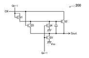
- FIG. 2 is a circuit diagram of a specific example of the shift register.
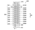
- FIG. 3 is a plan view of the TFT.
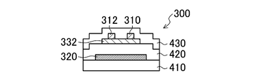
- FIG. 4 is a cross-sectional view taken along line IV-IV in FIG.
- FIG. 5 is a cross-sectional view taken along line VV in FIG.
- FIG. 6 is a flowchart showing a method for manufacturing a TFT.
- FIG. 7 is a plan view of the TFT.
- FIG. 8 is a plan view of the TFT.
- FIG. 9 is a graph showing the channel width dependence of the threshold voltage.
- FIG. 10 is a graph showing the gate voltage dependence of the drain current.
- FIG. 11 is a plan view of the TFT.
- FIG. 12 is a cross-sectional view taken along line XII-XII in FIG. 13 is a cross-sectional view taken along line XIII-XIII in FIG.
- FIG. 14 is a plan view of the TFT.
- FIG. 15 is a plan view of the TFT.
- 16 is a cross-sectional view taken along line XVI-XVI in FIG.
- FIG. 17 is a sectional view taken along line XVII-XVII in FIG.
- FIG. 18 is a plan view of the TFT.
- Coupled encompasses the term “directly connected” and is intended to be broader than this term. If A is directly connected to B and B is directly connected to C, then A can be said to be “coupled” to C. In other words, the term “coupled” includes the term “indirectly connected”.
- the term “on” used for two layers means at least somewhere between the layers. Means that contact exists.
- the word “over” means that the two layers are in close proximity, but one or more other layers may be in between, in which case the two layers are in contact However, it may not be in contact. Neither “above” nor “over” is intended to indicate direction, as used herein.
- the word “above” means that the first layer “over” the second layer, unless expressly stated otherwise, It is directly above the second layer and does not mean that it is in direct contact with the second layer. That is, there may be a third layer or other structure between the first layer and the second layer above the first layer.
- plan view is a view of the two main surfaces of the substrate as viewed from the side on which elements (eg, gates, source / drain electrodes) are formed.
- layer refers to any layer that can be formed by any suitable deposition process.
- layer includes layers specifically used in the semiconductor industry, including the liquid crystal display industry, including, but not limited to, conductive layers, insulating layers, and etch stopper layers.
- layer is synonymous with the term “film” often used in the semiconductor industry. These layers may be formed directly on the bottom surface of the substrate or may be formed on any of the various layers (or films). The layers are typically formed using the same material by the same steps, but are not limited thereto and may be formed using multiple steps or using different materials.
- channel width refers to two source / drain electrodes facing each other (for example, the source of the TFT 300) along the longitudinal direction of the source / drain electrodes (direction SD in the figure).
- the drain electrodes 310 and 312) indicate the length of overlapping in individual regions (for example, the region 331).
- the channel width is the contact provided on the two source / drain electrodes facing each other along the longitudinal direction of the source / drain electrodes (for example, TFT 1100 indicates the length of overlapping of the contacts 1131c1 and 1131c2).
- source / drain electrode is a generic term for a source electrode and a drain electrode. Therefore, if one of the two opposing source / drain electrodes functions as a source electrode, the other functions as a drain electrode.
- FIG. 1 is a block diagram of a gate driver of a liquid crystal display (LCD) 100.
- the LCD 100 includes a panel active area 110 and shift registers 150, 151 and 152.
- the panel active area 110 has pixels 110a to 110i. For simplicity, only nine pixels are shown in FIG. 1, but the panel active area 110 may include any number of pixels arranged in a matrix.
- the number of shift registers 150-152 can vary depending on the number of pixels 110a-110i.
- the ground Vss of the shift registers 150 to 152 is connected to the power supply ground Vss.
- the clock inputs CK of the shift registers 150 and 152 are connected to the gate clock GCK1.
- the clock input CK of the shift register 151 is connected to the gate clock GCK2.
- the output Gout of the shift register 150 is coupled to the gate lines of the pixels 110a to 110c.
- the input Qn ⁇ 1 of the shift register 150 receives the output Gout of the preceding stage (not shown).
- the input Qn + 1 of the shift register 150 receives the output Gout of the subsequent stage (shift register 151).
- the front stage refers to a stage located immediately above that stage, and the rear stage refers to a stage located directly below that stage. Therefore, the stage before the shift register 151 is the shift register 150.
- the subsequent stage of the shift register 151 is a shift register 152.
- the output Gout of the shift register 151 is coupled to the gate lines of the pixels 110d to 110f.
- the input Qn ⁇ 1 of the shift register 151 receives the output Gout of the preceding stage (shift register 150).
- the input Qn + 1 of the shift register 151 receives the output Gout of the subsequent stage (shift register 152).
- the output Gout of the shift register 152 is coupled to the gate lines of the pixels 110g to 110i.
- the input Qn ⁇ 1 of the shift register 152 receives the output Gout of the preceding stage (shift register 151).
- the input Qn + 1 of the shift register 152 receives the output Gout of the subsequent stage (not shown).
- Shift registers 150 to 152 sequentially drive the gate lines coupled to the output Gout.
- the specific configuration of the LCD 100 is not limited to that shown in FIG. 1, and any appropriate configuration can be used.
- FIG. 2 is a diagram of a circuit 200 that is a specific example of the shift registers 150 to 152.
- the circuit 200 includes transistors Q1 to Q5.
- the shift registers 150 to 152 are not limited to the circuit 200, and may be any appropriate circuit.
- Shift registers 150-152 may include any number of transistors.
- the drain current flowing through the transistors Q1 to Q5 differs depending on the configuration of the shift registers 150 to 152.
- the transistor Q2 in order to drive the gate line, the transistor Q2 needs to pass the largest drain current among the transistors Q1 to Q5.
- a large channel width is required to allow a large drain current to flow. Therefore, according to the prior art, the transistors Q1, Q2, Q3, Q4, and Q5 have channel widths of about 100 ⁇ m, about 500 ⁇ m, about 200 ⁇ m, about 100 ⁇ m, and about 50 ⁇ m, respectively.
- the thin film transistor (TFT) described below can be used as the transistor Q2, for example, but may be one of other transistors (for example, the transistors Q1, Q3, and Q4).
- FIG. 3 is a plan view of the TFT 300.
- FIG. 4 is a cross-sectional view taken along line IV-IV in FIG.
- FIG. 5 is a cross-sectional view taken along line VV in FIG.
- FIG. 6 is a flowchart illustrating a method 600 for manufacturing the TFT 300.
- the structure of the TFT 300 and the manufacturing method thereof will be described in detail with reference to FIGS.
- the TFT 300 includes source / drain electrodes 310 and 312, a gate electrode 320, and a semiconductor layer 330.
- the TFT 300 is used, for example, to realize an LCD gate driver, but is not limited to such an application example.
- the various TFTs disclosed herein can be utilized in any suitable circuit.
- the source / drain electrodes 310 and 312 have a laminated structure of Ti / Al / Ti.
- the source / drain electrodes 310 and 312 are not limited to the above structure, and can be made of any appropriate conductive material.
- the gate electrode 320 has a laminated structure of Ti / Al / Ti.
- the gate electrode 320 is not limited to the above structure, and can be made of any appropriate conductive material.
- the semiconductor layer 330 includes regions 331 to 340.
- the semiconductor layer 330 is made of an amorphous oxide semiconductor (hereinafter referred to as “IGZO”) containing indium (In), gallium (Ga), zinc (Zn), and oxygen (O) as main constituent elements.
- IGZO amorphous oxide semiconductor
- the TFT 300 is called an IGZO TFT.
- the semiconductor layer 330 includes a plurality of regions 331 to 340 divided in the longitudinal direction SD of the source / drain electrodes 310 and 312.
- the regions 331 to 340 have channel widths 331W to 340W, respectively.
- the channel widths 331W-340W are substantially the same, for example about 50 ⁇ m.
- the TFT 300 is equivalent to a transistor corresponding to the regions 331 to 340 coupled in parallel. Since these transistors have substantially the same channel width 331W to 340W, the threshold voltages of the individual transistors are also substantially equal.
- a gate electrode 320 is formed on the substrate 410.
- the substrate 410 is typically a glass substrate.
- the gate electrode 320 is formed by depositing a gate electrode material, patterning by photolithography, and then etching.
- the gate insulating film 420 is formed on the gate electrode 320.
- the gate insulating film 420 has a laminated structure of SiO2 / SiN.
- the gate insulating film 420 is formed by depositing a material for the gate insulating film.
- the semiconductor layer 330 is formed on the gate insulating film 420.
- the semiconductor layer 330 is formed by depositing IGZO, patterning by photolithography, and then etching.
- source / drain electrodes 310 and 312 are formed on the semiconductor layer 330.
- the source / drain electrodes 310 and 312 are formed by depositing a source / drain electrode material, patterning by photolithography, and then etching.
- a protective film 430 is formed on the source / drain electrodes 310 and 312.
- the protective film 430 is formed by depositing SiO2, patterning by photolithography, and then etching. At this time, the gate insulating film 420 and the protective film 430 are simultaneously etched.
- pixel electrodes are formed in the pixels 110a to 110i.
- the pixel electrode is formed by depositing indium tin oxide (ITO), patterning by photolithography, and then etching.
- ITO indium tin oxide
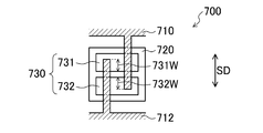
- FIG. 7 is a plan view of the TFT 700.
- the TFT 700 is the same as the TFT 300 except that the semiconductor layer 730 has two regions 731 and 732. Therefore, the manufacturing method of the TFT 700 is the same as the manufacturing method of the TFT 300.
- the TFT 700 has source / drain electrodes 710 and 712, a gate electrode 720, and a semiconductor layer 730.
- the source / drain electrodes 710 and 712 have a laminated structure of Ti / Al / Ti.
- the source / drain electrodes 710 and 712 are not limited to the above structure, and can be made of any appropriate conductive material.
- the gate electrode 720 has a laminated structure of Ti / Al / Ti.
- the gate electrode 720 is not limited to the above structure, and can be made of any appropriate conductive material.
- the semiconductor layer 730 includes regions 731 and 732.
- the semiconductor layer 730 is made of IGZO. As shown in FIG. 7, the semiconductor layer 730 includes a plurality of regions 731 and 732 divided in the longitudinal direction SD of the source / drain electrodes 710 and 712. Regions 731 and 732 have channel widths 731W and 732W, respectively. Typically, channel widths 731W and 732W are substantially the same, for example about 50 ⁇ m.
- the TFT 700 is equivalent to a transistor corresponding to the regions 731 and 732 coupled in parallel. Since these transistors have substantially the same channel widths 731W and 732W, the threshold voltages of the individual transistors are also substantially equal.
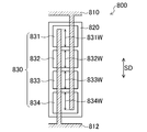
- FIG. 8 is a plan view of the TFT 800.
- the TFT 800 is the same as the TFT 300 except that the semiconductor layer 830 has four regions 831 to 834. Therefore, the manufacturing method of the TFT 800 is the same as the manufacturing method of the TFT 300.
- the TFT 800 includes source / drain electrodes 810 and 812, a gate electrode 820, and a semiconductor layer 830.
- the source / drain electrodes 810 and 812 have a laminated structure of Ti / Al / Ti.
- the source / drain electrodes 810 and 812 are not limited to the above structure, and may be made of any appropriate conductive material.
- the gate electrode 820 has a laminated structure of Ti / Al / Ti.
- the gate electrode 820 is not limited to the above structure, and can be made of any appropriate conductive material.
- the semiconductor layer 830 includes regions 831 to 834.
- the semiconductor layer 830 is made of IGZO. As shown in FIG. 8, the semiconductor layer 830 includes a plurality of regions 831 to 834 divided in the longitudinal direction SD of the source / drain electrodes 810 and 812. Regions 831-834 have channel widths 831W-834W, respectively. Typically, channel widths 831W-834W are substantially the same, for example about 125 ⁇ m.
- the TFT 800 is equivalent to a transistor corresponding to the regions 831 to 834 coupled in parallel. Since these transistors have substantially the same channel width 831W-834W, the threshold voltages of the individual transistors are also substantially equal.
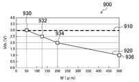
- FIG. 9 is a graph 900 showing the channel width dependence of the threshold voltage.
- the horizontal axis of the graph 900 indicates the channel width W [ ⁇ m], and the vertical axis of the graph 900 indicates the threshold voltage [V].
- a dotted line 910 is a threshold voltage Vth (for example, about 3.0 V) that a TFT used in a peripheral circuit (for example, a gate driver) of the LCD preferably has.
- a solid line 920 indicates a change in the threshold voltage Vth of the IGZO TFT when the channel width W is changed. In the conventional IGZO TFT, as indicated by the solid line 920, the threshold voltage Vth decreases as the channel width W increases.
- the threshold voltages Vth corresponding to channel widths W 200 ⁇ m (point 934) and 500 ⁇ m (point 936) are 2.0 V and 1.0 V, respectively, and these threshold voltages Vth are unacceptable for use as a peripheral circuit of the LCD.
- the threshold voltage Vth is about 3.0 V (point 930). Since the TFT 800 has a channel width of about 125 ⁇ m, the threshold voltage Vth is about 2.5 V (point 932). These threshold voltages (ie, about 2.5 V to about 3.0 V) realized by the TFTs 300, 700, and 800 according to the embodiment of the present invention are acceptable for use in the peripheral circuit of the LCD.
- the channel width W is preferably about 125 ⁇ m or less, more preferably about 50 ⁇ m or less.
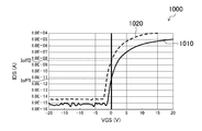
- FIG. 10 is a graph 1000 showing the gate voltage dependence of the drain current.
- the horizontal axis of the graph 1000 indicates the gate voltage VGS [V]
- the vertical axis of the graph 1000 indicates the drain current IDS [A].
- a solid line 1010 indicates the gate voltage dependence of the drain current for the TFT 300.
- Dashed line 1020 shows the gate voltage dependence of the drain current for a conventional IGZO TFT. The current that flows when the transistor is turned off is called leakage current and leads to unstable operation of the circuit. 10 that the drain current Ioff1 of the TFT 300 when the gate voltage VGS is zero is much lower than the drain current Ioff2 of the conventional TFT when the gate voltage VGS is zero. Therefore, the TFT 300 can contribute to stable operation of the circuit.
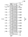
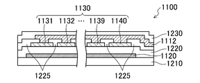
- FIG. 11 is a plan view of the TFT 1100.
- 12 is a cross-sectional view taken along line XII-XII in FIG. 13 is a cross-sectional view taken along line XIII-XIII in FIG.
- the TFT 1100 is the same as the TFT 300 except that the source / drain electrodes 1110 and 1112 have contacts 1131c1 and 1131c2, respectively, and the etching stopper layer 1225 is formed on the semiconductor layer 1130.
- the structure of the TFT 1100 and the manufacturing method thereof will be described in detail with reference to FIG. 6 and FIGS.
- the TFT 1100 includes source / drain electrodes 1110 and 1112, a gate electrode 1120, and a semiconductor layer 1130.
- the TFT 1100 is used for, for example, an LCD gate driver, but is not limited to such an application.
- the source / drain electrodes 1110 and 1112 have a laminated structure of Ti / Al / Ti.
- the source / drain electrodes 1110 and 1112 are not limited to the above structure, and may be made of any appropriate conductive material.
- the gate electrode 1120 has a laminated structure of Ti / Al / Ti.
- the gate electrode 1120 is not limited to the above structure, and can be made of a material having any appropriate conductivity.
- the semiconductor layer 1130 includes regions 1131 to 1140.
- the semiconductor layer 1130 is made of IGZO.
- the TFT 1100 is also called an IGZO TFT.
- the semiconductor layer 1130 includes a plurality of regions 1131 to 1140 divided in the longitudinal direction SD of the source / drain electrodes 1110 and 1112. Regions 1131 to 1140 have channel widths 1131W to 1140W, respectively. Typically, the channel widths 1131W to 1140W are substantially the same, for example about 50 ⁇ m.
- the TFT 1100 is equivalent to a transistor corresponding to the regions 1131 to 1140 coupled in parallel. Since these transistors have substantially the same channel width 1131W-1140W, the threshold voltages of the individual transistors are also substantially equal.
- a gate electrode 1120 is formed on the substrate 1210.
- the substrate 1210 is typically a glass substrate.
- the gate electrode 1120 is formed by depositing a gate electrode material, patterning by photolithography, and then etching.
- a gate insulating film 1220 is formed on the gate electrode 1120.
- the gate insulating film 1220 has a laminated structure of SiO2 / SiN.
- the gate insulating film 1220 is formed by depositing a material for the gate insulating film.
- the semiconductor layer 1130 is formed on the gate insulating film 1220.
- the semiconductor layer 1130 is formed by depositing IGZO, patterning by photolithography, and then etching.
- An etching stopper layer 1225 is formed after 606 and before 608.
- the etching stopper layer 1225 is formed by depositing, for example, silicon oxide, patterning by photolithography, and then etching.
- source / drain electrodes 1110, 1112 are formed on the semiconductor layer 1130.
- the source / drain electrodes 1110 and 1112 are formed by depositing a source / drain electrode material, patterning by photolithography, and then etching.
- a protective film 1230 is formed on the source / drain electrodes 1110, 1112.
- the protective film 1230 is formed by depositing SiO2, patterning by photolithography, and then etching. At this time, the gate insulating film 1220 and the protective film 1230 are etched simultaneously.
- pixel electrodes are formed in the pixels 110a to 110i.
- the pixel electrode is formed by depositing ITO, patterning by photolithography, and then etching.
- the etching stopper layer 1225 is formed between the semiconductor layer 1130 and the source / drain electrodes 1110 and 1112.
- An etching stopper layer 1225 is provided between the plurality of regions 1131 to 1140 of the semiconductor layer 1130.
- the etching stopper layer 1225 has 20 contact holes. These contact holes are arranged along a straight line parallel to the longitudinal direction of the source / drain electrodes 1110 and 1112. Contacts (for example, 1131c1 and 1131c2) of the source / drain electrodes 1110 and 1112 are in contact with the semiconductor layers 1131 to 1140 through these contact holes.
- the TFT 1100 has an effect that the etching stopper layer 1225 can protect the channel region under the source / drain electrodes from the etching process.
- an etching stopper layer 1225 is provided between the regions 1131 to 1140.
- the channel region can be better protected as compared with the case where the etching stopper layer 1225 is not provided between the regions 1131 to 1140.
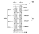
- FIG. 14 is a plan view of the TFT 1400.
- the TFT 1400 is similar to the TFT 1100 except that the semiconductor layer 1430 has four regions 1431 to 1434. Therefore, the manufacturing method of the TFT 1400 is the same as the manufacturing method of the TFT 1100.
- the TFT 1400 includes source / drain electrodes 1410 and 1412, a gate electrode 1420, and a semiconductor layer 1430.
- the source / drain electrodes 1410 and 1412 have a laminated structure of Ti / Al / Ti.
- the source / drain electrodes 1410 and 1412 are not limited to the above structure, and may be made of any appropriate conductive material.
- the gate electrode 1420 has a laminated structure of Ti / Al / Ti.
- the gate electrode 1420 is not limited to the above structure, and can be made of any appropriate conductive material.
- the semiconductor layer 1430 includes regions 1431 to 1434.
- the semiconductor layer 1430 is made of IGZO. As shown in FIG. 14, the semiconductor layer 1430 includes a plurality of regions 1431 to 1434 divided in the longitudinal direction SD of the source / drain electrodes 1410 and 1412. Regions 1431 to 1434 have channel widths 1431W to 1434W, respectively. Typically, channel widths 1431W-1434W are substantially the same, for example about 125 ⁇ m.
- the TFT 1400 is equivalent to a transistor corresponding to the regions 1431 to 1434 coupled in parallel. Since these transistors have substantially the same channel widths 1431W-1434W, the threshold voltages of the individual transistors are also substantially equal.
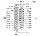
- FIG. 15 is a plan view of the TFT 1500.
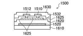
- 16 is a cross-sectional view taken along line XVI-XVI in FIG.
- FIG. 17 is a sectional view taken along line XVII-XVII in FIG.
- the TFT 1500 is the same as the TFT 300 except that the source / drain electrodes 1510 and 1512 have contacts 1531c1 and 1531c2, respectively, and the etching stopper layer 1225 is formed on the semiconductor layer 1530.
- the structure of the TFT 1500 and the manufacturing method thereof will be described in detail with reference to FIG. 6 and FIGS.
- the TFT 1500 includes source / drain electrodes 1510 and 1512, a gate electrode 1520, and a semiconductor layer 1530.
- the TFT 1500 is used for, for example, an LCD gate driver, but is not limited to such an application.
- the source / drain electrodes 1510 and 1512 have a laminated structure of Ti / Al / Ti.
- the source / drain electrodes 1510 and 1512 are not limited to the above structure, and may be made of any appropriate conductive material.
- the gate electrode 1520 has a laminated structure of Ti / Al / Ti.
- the gate electrode 1520 is not limited to the above structure, and can be made of any appropriate conductive material.
- the semiconductor layer 1530 includes regions 1531 to 1540.
- the semiconductor layer 1530 is made of IGZO.
- the TFT 1500 is also called an IGZO TFT.
- the semiconductor layer 1530 includes a plurality of regions 1531 to 1540 divided in the longitudinal direction SD of the source / drain electrodes 1510 and 1512. Regions 1531 to 1540 have channel widths 1531W to 1540W, respectively. Typically, the channel widths 1531W-1540W are substantially the same, for example about 50 ⁇ m.
- the TFT 1500 is equivalent to a transistor corresponding to the regions 1531 to 1540 coupled in parallel. Since these transistors have substantially the same channel width 1531W-1540W, the threshold voltages of the individual transistors are also substantially equal.
- a gate electrode 1520 is formed on the substrate 1610.
- the substrate 1610 is typically a glass substrate.
- the gate electrode 1520 is formed by depositing a gate electrode material, patterning by photolithography, and then etching.
- a gate insulating film 1620 is formed on the gate electrode 1520.
- the gate insulating film 1620 has a laminated structure of SiO2 / SiN.
- the gate insulating film 1620 is formed by depositing a material for the gate insulating film.
- a semiconductor layer 1530 is formed on the gate insulating film 1620.
- the semiconductor layer 1530 is formed by depositing IGZO, patterning by photolithography, and then etching.
- An etching stopper layer 1625 is formed after 606 and before 608.
- the etching stopper layer 1625 is formed, for example, by depositing silicon oxide, patterning by photolithography, and then etching.
- source / drain electrodes 1510 and 1512 are formed on the semiconductor layer 1530.
- the source / drain electrodes 1510 and 1512 are formed by depositing the material of the source / drain electrodes, patterning by photolithography, and then etching.
- a protective film 1630 is formed on the source / drain electrodes 1510 and 1512.
- the protective film 1630 is formed by depositing SiO2, patterning by photolithography, and then etching. At this time, the gate insulating film 1620 and the protective film 1630 are etched simultaneously.
- pixel electrodes are formed in the pixels 110a to 110i.
- the pixel electrode is formed by depositing ITO, patterning by photolithography, and then etching.
- the etching stopper layer 1625 is formed between the semiconductor layer 1530 and the source / drain electrodes 1510 and 1512.
- Source / drain electrodes 1510 and 1512 are provided between the plurality of regions 1531 to 1540 of the semiconductor layer 1530.
- the etching stopper layer 1625 has two elongated contact holes. These contact holes are parallel to the longitudinal direction of the source / drain electrodes 1510 and 1512.
- the contacts (for example, 1531c1 and 1531c2) of the source / drain electrodes 1510 and 1512 are in contact with the semiconductor layers 1531 to 1540 through these contact holes.
- the TFT 1500 has an effect that the etching stopper layer 1625 can protect the channel region under the source / drain electrodes from the etching process in addition to the effect of the TFT 300.
- the etching stopper layer 1225 of the TFT 1100 has 20 contact holes
- the etching stopper layer 1625 of the TFT 1500 only has two elongated contact holes.
- the TFT 1500 can reduce the device area while preventing the channel width W from becoming narrow.
- the TFT 1500 also has the effect of reducing the device area without reducing the current drive capability.
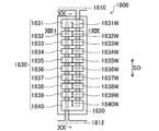
- FIG. 18 is a plan view of the TFT 1800.
- FIG. 19 is a sectional view taken along line XIX-XIX in FIG. 20 is a cross-sectional view taken along line XX-XX in FIG.
- the structure of the TFT 1800 and the manufacturing method thereof will be described in detail with reference to FIGS. 18 to 20 and FIG.
- the TFT 1800 includes source / drain electrodes 1810 and 1812, a gate electrode 1820, and a semiconductor layer 1830.
- the TFT 1800 is used, for example, to realize an LCD gate driver, but is not limited to such an application example.
- the source / drain electrodes 1810 and 1812 have a laminated structure of Ti / Al / Ti.
- the source / drain electrodes 1810 and 1812 are not limited to the above structure, and can be made of any appropriate conductive material.
- the gate electrode 1820 has a laminated structure of Ti / Al / Ti.
- the gate electrode 1820 is not limited to the above structure, and can be made of any appropriate conductive material.
- the semiconductor layer 1830 includes regions 1831 to 1840.
- the semiconductor layer 1830 is made of an amorphous oxide semiconductor (hereinafter referred to as “IGZO”) containing indium (In), gallium (Ga), zinc (Zn), and oxygen (O) as main constituent elements.
- IGZO amorphous oxide semiconductor
- the TFT 1800 is called an IGZO TFT.
- the semiconductor layer 1830 includes a plurality of regions 1831 to 1840 divided in the longitudinal direction SD of the source / drain electrodes 1810 and 1812.
- the regions 1831 to 1840 have channel widths 1831W to 1840W, respectively.
- the channel widths 1831W-1840W are substantially the same, for example about 50 ⁇ m.
- the TFT 1800 is equivalent to a transistor corresponding to the regions 1831 to 1840 coupled in parallel. Since these transistors have substantially the same channel width 1831W-1840W, the threshold voltages of the individual transistors are also substantially equal.
- the manufacturing method of the TFT 1800 is the same as that of the TFT 300 shown in FIG. 6 except that the source / drain electrodes 1810 and 1812 are first formed in 608 and then the semiconductor layer 1830 is formed in 606.
- the substrate 1910, the gate insulating film 1920, and the protective film 1930 correspond to the substrate 410, the gate insulating film 420, and the protective film 430, respectively, and have the same structure and function as these.
- the semiconductor layer 1830 of the TFT 1800 covers the source / drain electrodes 1810 and 1812. As can be understood by comparing FIG. 19 with FIG. 4, the TFTs 300 and 1800 have different positional relationships between the source / drain electrodes and the semiconductor layer with respect to the substrate. However, due to the structure in which the semiconductor layer 1830 is located near the source / drain electrodes 1810 and 1812, the TFT 1800 operates in the same manner as the TFT 300, and thereby has the same effect as the TFT 300.
- TFTs 300, 700, 800, 1100, 1400, 1500, 1800 are used for, for example, a shift register (for example, shift register 200) included in a gate driver of an LCD. It is done. At this time, the above-described TFT can be used, for example, for a transistor that requires the largest drain current to flow.
- the TFT 300 is used as the transistor Q2 of the shift register 200.
- a transistor corresponding to a plurality of regions of the TFT 300 has a channel width W1 (for example, 50 ⁇ m), and among the channel widths of the other transistors Q1, Q3 to Q5 included in the shift register 200, the smallest one is the channel width W2. (For example, 50 ⁇ m of the transistor Q5). At this time, the channel width W1 is substantially equal to the channel width W2. When this condition for channel width is met, transistors Q1-Q5 in shift register 200 have approximately equal thresholds. As a result, it is possible to reduce the leakage current of the transistors of the shift register 200 as a whole.
- the above-described TFT is a bottom gate type (also referred to as an inverted stagger type) in which the gate electrode is closer to the substrate than the source / drain electrodes.
- the embodiment of the present invention can also be realized as a top gate type (also called stagger type) TFT.
- the TFT according to the embodiment of the present specification may be used for applications other than the LCD.
- the material of the substrate is not limited to glass and can be any other suitable material.
Landscapes
- Thin Film Transistor (AREA)
- Chemical & Material Sciences (AREA)
- Crystallography & Structural Chemistry (AREA)
- Liquid Crystal (AREA)
Abstract
大電流駆動能力と、適正な閾値電圧とを有する薄膜トランジスタを提供する。ゲート電極と、ゲート電極上に形成された絶縁層と、前記絶縁層上に形成された半導体層と、前記半導体層上に形成されたソース・ドレイン電極とを備える薄膜トランジスタであって、前記半導体層は、前記ソース・ドレイン電極の長手方向に分割された複数領域を含む。
Description
本開示は、インジウム・ガリウム・亜鉛複合酸化物(IGZO)を用いた薄膜トランジスタ、および薄膜トランジスタを用いたシフトレジスタに関する。
薄膜トランジスタ(TFT)は、電界効果型トランジスタの一種である。TFTは、液晶ディスプレイ(LCD)パネルの画素を駆動するためなどに広く利用されている。トランジスタの特性に影響するパラメータにチャネル長Lおよびチャネル幅Wがある。
特許文献1は、トランジスタの特性を変化させるために、チャネル長Lに対するチャネル幅Wの比W/Lを変えることについて記載している。
LCDパネルを駆動するためには、ゲートドライバおよびソースドライバが用いられる。ゲートドライバには、ゲート線に対応するシフトレジスタが設けられる。それぞれのシフトレジスタには、典型的には数個のトランジスタが用いられる。シフトレジスタにおいて、ゲート線に電流を出力するトランジスタ(出力トランジスタ)は、他のトランジスタに比べて、大電流の駆動能力が必要である。
大電流で駆動するためには、トランジスタは大きいチャネル幅を有する必要がある。IGZOを用いたTFT(IGZO TFT)のチャネル幅が大きいと、閾値電圧が下がる。この場合、トランジスタがターンオフしている時のリーク電流も増えてしまう。換言すれば従来のIGZO TFTは、大電流駆動能力を提供しつつ、リーク電流の増加しない適切な閾値を得ることができなかった。
特許文献1は、アモルファスシリコン(a-Si)TFTの使用を想定するが、IGZO TFTを使用する具体的な手法についての示唆を与えるものではない。例えば特許文献1は、閾値電圧のチャネル幅依存性について考慮していない。
上記を鑑みて、本発明の目的は、大電流駆動能力と、適正な閾値電圧とを有する薄膜トランジスタを提供することにある。本発明の他の目的は、トランジスタのリーク電流を全体として減少させることができるシフトレジスタを提供することにある。
本発明のある実施形態による薄膜トランジスタは、ゲート電極と、ゲート電極上に形成された絶縁層と、前記絶縁層上に形成された半導体層と、前記半導体層上に形成されたソース・ドレイン電極とを備え、前記半導体層は、前記ソース・ドレイン電極の長手方向に分割された複数領域を含む。
上記構成により、大電流駆動能力と、適正な閾値電圧とを有する薄膜トランジスタを提供できる。
ある具体的な実施形態によれば、前記複数領域に対応するトランジスタのチャネル幅Wは、約125μm以下である。
上記構成により、より高い閾値電圧を実現できる。
ある具体的な実施形態によれば、前記複数領域に対応するトランジスタのチャネル幅Wは、約50μm以下である。
上記構成により、チャネル幅Wが約125μmの場合よりも高い閾値電圧を実現できる。
ある具体的な実施形態によれば、エッチングストッパ層が前記半導体層と前記ソース・ドレイン電極との間に形成されている。
上記構成により、エッチングストッパ層がソース・ドレイン電極下のチャネル領域をエッチング処理から保護できる。
ある具体的な実施形態によれば、前記複数領域の間には、前記エッチングストッパ層が設けられている。
上記構成により、複数領域の間にエッチングストッパ層が設けられていない場合と比較して、チャネル領域をよりよく保護できる。
ある具体的な実施形態によれば、前記複数領域の間には、前記ソース・ドレイン電極が設けられている。
上記構成により、チャネル幅が狭くなることを防ぎつつ、そのデバイス面積を縮小できる。換言すれば電流駆動能力を低下させることなく、デバイス面積を小さくできる。
本発明のある実施形態による薄膜トランジスタは、ゲート電極と、ゲート電極上に形成された絶縁層と、前記絶縁層上に形成されたソース・ドレイン電極と、前記ソース・ドレイン電極上に形成された半導体層と、を備える薄膜トランジスタであって、前記半導体層は、前記ソース・ドレイン電極の長手方向に分割された複数領域を含む。
上記構成により、大電流駆動能力と、適正な閾値電圧とを有する薄膜トランジスタを提供できる。
本発明のある実施形態によるシフトレジスタは、複数の薄膜トランジスタを備えるシフトレジスタであって、前記複数の薄膜トランジスタは、ゲート電極と、ゲート電極上に形成された絶縁層と、前記絶縁層上に形成された半導体層と、前記半導体層上に形成されたソース・ドレイン電極とを含む第1薄膜トランジスタであって、前記半導体層は、前記ソース・ドレイン電極の長手方向に分割された複数領域を含む第1薄膜トランジスタと、第2薄膜トランジスタとを含み、前記第1薄膜トランジスタの前記複数領域は、第1チャネル幅を有し、前記第2薄膜トランジスタは、前記第1の薄膜トランジスタ以外の前記複数の薄膜トランジスタのうち、最も小さい第2チャネル幅を有し、前記第1チャネル幅W1は、実質的に前記第2チャネル幅と等しい。
上記構成により、シフトレジスタ内のトランジスタがほぼ等しい閾値を有する。その結果、シフトレジスタのトランジスタのリーク電流を全体として減少させることができるという効果を奏する。
本発明によれば、大電流駆動能力と、適正な閾値電圧とを有する薄膜トランジスタを提供することができる。本発明によれば、トランジスタのリーク電流を全体として減少させることができるシフトレジスタを提供することができる。
本発明の例示的実施形態による薄膜トランジスタについて、図面を参照して詳細に説明する。図面において同一または同様の構成要素は、同じ参照符号によって表される。
(用語および定義)
「結合される」という語は、「直接的に接続される」という語を包含し、この語よりも広いと意図される。もしAがBに直接的に接続され、BがCに直接的に接続されるなら、AはCに「結合される」と言える。換言すれば「結合される」という語は、「間接的に接続される」という語を含む。
「結合される」という語は、「直接的に接続される」という語を包含し、この語よりも広いと意図される。もしAがBに直接的に接続され、BがCに直接的に接続されるなら、AはCに「結合される」と言える。換言すれば「結合される」という語は、「間接的に接続される」という語を含む。
本明細書および特許請求の範囲において、「層A上に形成された層B」というような、ある2つの層について用いられる「~の上に」という語は、それらの層の間に少なくともなんらかの接触が存在することを意味する。「~を覆って」という語は、その2層が近接して存在することを意味するが、1つ以上の別の層が間に存在してもよく、その場合、2層が接触してもよいが、接触していなくてもよい。「~の上に」も「~を覆って」も、ここで用いられるように、方向を表すものではない。
本明細書および特許請求の範囲で用いられるように、「~の上に」という語は、明示的にその旨が述べられていない限り、第2層「の上にある」第1層が、第2層の直上にあり、第2層に直接に接触していることを意味しない。つまり第1層と、第1層の上にある第2層との間には第3層または他の構造が存在し得る。
「平面図」という語は、基板の2つの主面のうち、要素(例えばゲート、ソース・ドレイン電極)が形成される側から見た図である。
「層」という語は、任意の適切な堆積プロセスによって形成され得る任意の層を指す。「層」という語は、液晶ディスプレイ業界を含む半導体業界で特に用いられる層を含み、例えば、これらには限定されないが、導電性層、絶縁層、およびエッチングストッパ層を含む。「層」という語は、半導体業界でよく用いられる「膜」という語と同義である。これら層は、基板の最も下の表面上に直接に形成されてもよく、またはさまざまな層(または膜)の任意のものの上に形成されてもよい。層は、典型的には同じステップによって同じ材料を用いて形成されるが、これには限定されず、複数のステップを用いて、または異なる材料を用いて形成されてもよい。
本明細書および特許請求の範囲において、「チャネル幅」という語は、ソース・ドレイン電極の長手方向(図中、方向SD)に沿って、対向する2つのソース・ドレイン電極(例えばTFT 300のソース・ドレイン電極310,312)が、個々の領域(例えば領域331)内で重なる長さを指す。ソース・ドレイン電極にコンタクトが設けられる場合(TFT 1100,1500など)は、チャネル幅は、ソース・ドレイン電極の長手方向に沿って、対向する2つのソース・ドレイン電極に設けられたコンタクト(例えばTFT 1100のコンタクト1131c1,1131c2)が重なる長さを指す。
ソース・ドレイン電極という語は、ソース電極およびドレイン電極を総称する。したがって2つの対向するソース・ドレイン電極のいずれか一方がソース電極として機能すれば、他方はドレイン電極として機能する。
(システムの概略)
図1は、液晶ディスプレイ(LCD)100のゲートドライバのブロック図である。LCD 100は、パネルアクティブエリア110、シフトレジスタ150,151,152を含む。パネルアクティブエリア110は、画素110a~110iを有する。簡単のために図1では、9つの画素しか示されないが、パネルアクティブエリア110は、マトリックス状に配置された任意の個数の画素を含み得る。シフトレジスタ150~152の個数は、画素110a~110iの個数に依存して変わり得る。
図1は、液晶ディスプレイ(LCD)100のゲートドライバのブロック図である。LCD 100は、パネルアクティブエリア110、シフトレジスタ150,151,152を含む。パネルアクティブエリア110は、画素110a~110iを有する。簡単のために図1では、9つの画素しか示されないが、パネルアクティブエリア110は、マトリックス状に配置された任意の個数の画素を含み得る。シフトレジスタ150~152の個数は、画素110a~110iの個数に依存して変わり得る。
シフトレジスタ150~152のグランドVssは、電源のグランドVssに接続される。シフトレジスタ150,152のクロック入力CKは、ゲートクロックGCK1に接続される。シフトレジスタ151のクロック入力CKは、ゲートクロックGCK2に接続される。
シフトレジスタ150の出力Goutは、画素110a~110cのゲート線に結合される。シフトレジスタ150の入力Qn-1は、その前段(不図示)の出力Goutを受け取る。シフトレジスタ150の入力Qn+1は、その後段(シフトレジスタ151)の出力Goutを受け取る。図1において、前段とは、その段の直上に位置する段を指し、後段とは、その段の直下に位置する段を指す。よってシフトレジスタ151の前段は、シフトレジスタ150である。シフトレジスタ151の後段は、シフトレジスタ152である。
シフトレジスタ151の出力Goutは、画素110d~110fのゲート線に結合される。シフトレジスタ151の入力Qn-1は、その前段(シフトレジスタ150)の出力Goutを受け取る。シフトレジスタ151の入力Qn+1は、その後段(シフトレジスタ152)の出力Goutを受け取る。
シフトレジスタ152の出力Goutは、画素110g~110iのゲート線に結合される。シフトレジスタ152の入力Qn-1は、その前段(シフトレジスタ151)の出力Goutを受け取る。シフトレジスタ152の入力Qn+1は、その後段(不図示)の出力Goutを受け取る。
シフトレジスタ150~152は、出力Goutに結合されたゲート線を逐次、駆動する。LCD 100の具体的な構成は、図1に示すものには限定されず、任意の適切な構成を用いることができる。
図2は、シフトレジスタ150~152の具体例である回路200の図である。回路200は、トランジスタQ1~Q5を有する。シフトレジスタ150~152は、回路200には限定されず、任意の適切な回路であり得る。シフトレジスタ150~152は、任意の個数のトランジスタを含み得る。
トランジスタQ1~Q5を流れるドレイン電流は、シフトレジスタ150~152の構成によって異なる。ここではゲート線を駆動するために、トランジスタQ2がトランジスタQ1~Q5のうち最も大きいドレイン電流を流す必要がある。従来技術によれば、大きいドレイン電流を流すことを可能にするためには、大きいチャネル幅を必要とした。そのため、従来の技術によれば、トランジスタQ1,Q2,Q3,Q4,Q5は、例えばそれぞれ約100μm,約500μm,約200μm,約100μm,約50μmのチャネル幅を有することになる。
以下に説明される薄膜トランジスタ(TFT)は、例えばトランジスタQ2として利用され得るが、他のトランジスタ(例えばトランジスタQ1,Q3,およびQ4)のうちの1つであってもよい。
(TFTの構造)
図3は、TFT 300の平面図である。図4は、図3の線IV-IVに沿った断面図である。図5は、図3の線V-Vに沿った断面図である。図6は、TFT 300を製造する方法600を示すフローチャートである。以下、図3~図6を参照して、TFT 300の構造およびその製造方法を詳細に説明する。
図3は、TFT 300の平面図である。図4は、図3の線IV-IVに沿った断面図である。図5は、図3の線V-Vに沿った断面図である。図6は、TFT 300を製造する方法600を示すフローチャートである。以下、図3~図6を参照して、TFT 300の構造およびその製造方法を詳細に説明する。
TFT 300は、ソース・ドレイン電極310,312、ゲート電極320、および半導体層330を有する。TFT 300は、例えばLCDのゲートドライバを実現するのに利用されるが、このような応用例には限定されない。本明細書で開示されるさまざまなTFT(具体的にはTFT 300,700,800,1100,1400,1500,1800)は、任意の適切な回路において利用され得る。
ソース・ドレイン電極310,312は、Ti/Al/Tiの積層構造を有する。ソース・ドレイン電極310,312は、上記構造には限定されず、任意の適切な導電性を有する材質から作られ得る。
ゲート電極320は、Ti/Al/Tiの積層構造を有する。ゲート電極320は、上記構造には限定されず、任意の適切な導電性を有する材質から作られ得る。
半導体層330は、領域331~340を含む。半導体層330は、インジウム(In)、ガリウム(Ga)、亜鉛(Zn)、酸素(O)を主要な構成元素として含むアモルファス酸化物半導体(以下「IGZO」と呼ぶ)でできている。ここではTFT 300は、IGZO TFTと呼ばれる。
図3に示すように半導体層330は、ソース・ドレイン電極310,312の長手方向SDに分割された複数領域331~340を含む。領域331~340は、それぞれチャネル幅331W~340Wを有する。典型的にはチャネル幅331W~340Wは、実質的に同じであり、例えば約50μmである。TFT 300は、並列に結合された領域331~340に対応するトランジスタと等価である。これらトランジスタは、実質的に同じチャネル幅331W~340Wを有するので、個々のトランジスタの閾値電圧も実質的に等しい。
(TFTの製造方法)
602において、基板410の上にゲート電極320が形成される。基板410は、典型的にはガラス基板である。ゲート電極320は、ゲート電極の材料を堆積し、フォトリソグラフィによってパターニングし、その後、エッチングすることによって形成される。
602において、基板410の上にゲート電極320が形成される。基板410は、典型的にはガラス基板である。ゲート電極320は、ゲート電極の材料を堆積し、フォトリソグラフィによってパターニングし、その後、エッチングすることによって形成される。
604において、ゲート電極320の上にゲート絶縁膜420が形成される。ゲート絶縁膜420は、SiO2/SiNの積層構造を有する。ゲート絶縁膜420は、ゲート絶縁膜の材料を堆積することによって形成される。
606において、ゲート絶縁膜420の上に半導体層330が形成される。半導体層330は、IGZOを堆積し、フォトリソグラフィによってパターニングし、その後、エッチングすることによって形成される。
608において、半導体層330の上にソース・ドレイン電極310,312が形成される。ソース・ドレイン電極310,312は、ソース・ドレイン電極の材料を堆積し、フォトリソグラフィによってパターニングし、その後、エッチングすることによって形成される。
610において、ソース・ドレイン電極310,312の上に保護膜430が形成される。保護膜430は、SiO2を堆積し、フォトリソグラフィによってパターニングし、その後、エッチングすることによって形成される。このときゲート絶縁膜420と保護膜430とは、同時にエッチングされる。
612において、画素110a~110i内に画素電極が形成される。画素電極は、酸化インジウムスズ(ITO)を堆積し、フォトリソグラフィによってパターニングし、その後、エッチングすることによって形成される。
図7は、TFT 700の平面図である。TFT 700は、半導体層730が2つの領域731,732を有することを除けば、TFT 300と同様である。よってTFT 700の製造方法は、TFT 300の製造方法と同様である。
TFT 700は、ソース・ドレイン電極710,712、ゲート電極720、および半導体層730を有する。
ソース・ドレイン電極710,712は、Ti/Al/Tiの積層構造を有する。ソース・ドレイン電極710,712は、上記構造には限定されず、任意の適切な導電性を有する材質から作られ得る。
ゲート電極720は、Ti/Al/Tiの積層構造を有する。ゲート電極720は、上記構造には限定されず、任意の適切な導電性を有する材質から作られ得る。
半導体層730は、領域731および732を含む。半導体層730は、IGZOでできている。図7に示すように半導体層730は、ソース・ドレイン電極710,712の長手方向SDに分割された複数領域731および732を含む。領域731および732は、それぞれチャネル幅731Wおよび732Wを有する。典型的にはチャネル幅731Wおよび732Wは、実質的に同じであり、例えば約50μmである。TFT 700は、並列に結合された領域731および732に対応するトランジスタと等価である。これらトランジスタは、実質的に同じチャネル幅731Wおよび732Wを有するので、個々のトランジスタの閾値電圧も実質的に等しい。
図8は、TFT 800の平面図である。TFT 800は、半導体層830が4つの領域831~834を有することを除けば、TFT 300と同様である。よってTFT 800の製造方法は、TFT 300の製造方法と同様である。
TFT 800は、ソース・ドレイン電極810,812、ゲート電極820、および半導体層830を有する。
ソース・ドレイン電極810,812は、Ti/Al/Tiの積層構造を有する。ソース・ドレイン電極810,812は、上記構造には限定されず、任意の適切な導電性を有する材質から作られ得る。
ゲート電極820は、Ti/Al/Tiの積層構造を有する。ゲート電極820は、上記構造には限定されず、任意の適切な導電性を有する材質から作られ得る。
半導体層830は、領域831~834を含む。半導体層830は、IGZOでできている。図8に示すように半導体層830は、ソース・ドレイン電極810,812の長手方向SDに分割された複数領域831~834を含む。領域831~834は、それぞれチャネル幅831W~834Wを有する。典型的にはチャネル幅831W~834Wは、実質的に同じであり、例えば約125μmである。TFT 800は、並列に結合された領域831~834に対応するトランジスタと等価である。これらトランジスタは、実質的に同じチャネル幅831W~834Wを有するので、個々のトランジスタの閾値電圧も実質的に等しい。
(閾値電圧)
図9は、閾値電圧のチャネル幅依存性を示すグラフ900である。グラフ900の横軸はチャネル幅W[μm]を示し、グラフ900の縦軸は閾値電圧[V]を示す。点線910は、LCDの周辺回路(例えばゲートドライバ)において用いられるTFTが有するのが好ましい閾値電圧Vth(例えば約3.0V)である。実線920は、チャネル幅Wが変化したときのIGZO TFTの閾値電圧Vthの変化を示す。従来のIGZO TFTは、実線920に示されるように、チャネル幅Wが大きくなる従って閾値電圧Vthが減少する。例えばチャネル幅W200μm(点934)および500μm(点936)に対応する閾値電圧Vthはそれぞれ2.0Vおよび1.0Vであり、これら閾値電圧Vthは、LCDの周辺回路として使うには許容できない。
図9は、閾値電圧のチャネル幅依存性を示すグラフ900である。グラフ900の横軸はチャネル幅W[μm]を示し、グラフ900の縦軸は閾値電圧[V]を示す。点線910は、LCDの周辺回路(例えばゲートドライバ)において用いられるTFTが有するのが好ましい閾値電圧Vth(例えば約3.0V)である。実線920は、チャネル幅Wが変化したときのIGZO TFTの閾値電圧Vthの変化を示す。従来のIGZO TFTは、実線920に示されるように、チャネル幅Wが大きくなる従って閾値電圧Vthが減少する。例えばチャネル幅W200μm(点934)および500μm(点936)に対応する閾値電圧Vthはそれぞれ2.0Vおよび1.0Vであり、これら閾値電圧Vthは、LCDの周辺回路として使うには許容できない。
これに対してTFT 300,700はチャネル幅約50μmを有するので、閾値電圧Vthは約3.0V(点930)である。TFT 800はチャネル幅約125μmを有するので、閾値電圧Vthは約2.5V(点932)である。本発明の実施形態によるTFT 300,700,800が実現するこれらの閾値電圧(すなわち約2.5V~約3.0V)は、LCDの周辺回路において利用するのに許容できる。したがって本発明のさまざまな実施形態において、チャネル幅Wは、好ましくは約125μm以下であり、より好ましくは約50μm以下である。
以上より本発明の実施形態によれば、従来のIGZO TFTと比較して、大電流駆動能力と、適正な閾値電圧とを有する薄膜トランジスタを実現できる。
(リーク電流)
図10は、ドレイン電流のゲート電圧依存性を示すグラフ1000である。グラフ1000の横軸はゲート電圧VGS[V]を示し、グラフ1000の縦軸はドレイン電流IDS[A]を示す。実線1010は、TFT 300についてのドレイン電流のゲート電圧依存性を示す。破線1020は、従来のIGZO TFTについてのドレイン電流のゲート電圧依存性を示す。トランジスタがターンオフされているときに流れる電流はリーク電流と呼ばれ、回路の不安定な動作をつながる。図10から、ゲート電圧VGSがゼロのときのTFT 300のドレイン電流Ioff1は、ゲート電圧VGSがゼロのときの従来のTFTのドレイン電流Ioff2よりもかなり低いことがわかる。したがってTFT 300は、回路の安定な動作に寄与し得る。
図10は、ドレイン電流のゲート電圧依存性を示すグラフ1000である。グラフ1000の横軸はゲート電圧VGS[V]を示し、グラフ1000の縦軸はドレイン電流IDS[A]を示す。実線1010は、TFT 300についてのドレイン電流のゲート電圧依存性を示す。破線1020は、従来のIGZO TFTについてのドレイン電流のゲート電圧依存性を示す。トランジスタがターンオフされているときに流れる電流はリーク電流と呼ばれ、回路の不安定な動作をつながる。図10から、ゲート電圧VGSがゼロのときのTFT 300のドレイン電流Ioff1は、ゲート電圧VGSがゼロのときの従来のTFTのドレイン電流Ioff2よりもかなり低いことがわかる。したがってTFT 300は、回路の安定な動作に寄与し得る。
(エッチングストッパ層)
図11は、TFT 1100の平面図である。図12は、図11の線XII-XIIに沿った断面図である。図13は、図11の線XIII-XIIIに沿った断面図である。TFT 1100は、ソース・ドレイン電極1110,1112がそれぞれコンタクト1131c1、1131c2などを有すること、およびエッチングストッパ層1225が半導体層1130の上に形成されることを除けば、TFT 300と同様である。図6および図11~図13を参照して、TFT 1100の構造およびその製造方法を詳細に説明する。
図11は、TFT 1100の平面図である。図12は、図11の線XII-XIIに沿った断面図である。図13は、図11の線XIII-XIIIに沿った断面図である。TFT 1100は、ソース・ドレイン電極1110,1112がそれぞれコンタクト1131c1、1131c2などを有すること、およびエッチングストッパ層1225が半導体層1130の上に形成されることを除けば、TFT 300と同様である。図6および図11~図13を参照して、TFT 1100の構造およびその製造方法を詳細に説明する。
TFT 1100は、ソース・ドレイン電極1110,1112、ゲート電極1120、および半導体層1130を有する。TFT 1100は、例えばLCDのゲートドライバに利用されるが、このような応用例には限定されない。
ソース・ドレイン電極1110,1112は、Ti/Al/Tiの積層構造を有する。ソース・ドレイン電極1110,1112は、上記構造には限定されず、任意の適切な導電性を有する材質から作られ得る。
ゲート電極1120は、Ti/Al/Tiの積層構造を有する。ゲート電極1120は、上記構造には限定されず、任意の適切な導電性を有する材質から作られ得る。
半導体層1130は、領域1131~1140を含む。半導体層1130は、IGZOでできている。TFT 1100も、IGZO TFTと呼ばれる。
図11に示すように半導体層1130は、ソース・ドレイン電極1110,1112の長手方向SDに分割された複数領域1131~1140を含む。領域1131~1140は、それぞれチャネル幅1131W~1140Wを有する。典型的にはチャネル幅1131W~1140Wは、実質的に同じであり、例えば約50μmである。TFT 1100は、並列に結合された領域1131~1140に対応するトランジスタと等価である。これらトランジスタは、実質的に同じチャネル幅1131W~1140Wを有するので、個々のトランジスタの閾値電圧も実質的に等しい。
コンタクト1131c1,1131c2と同様のコンタクトが領域1132~1140についても設けられる。
以下、再び図6を参照して、TFT 1100の製造方法を説明する。
602において、基板1210の上にゲート電極1120が形成される。基板1210は、典型的にはガラス基板である。ゲート電極1120は、ゲート電極の材料を堆積し、フォトリソグラフィによってパターニングし、その後、エッチングすることによって形成される。
604において、ゲート電極1120の上にゲート絶縁膜1220が形成される。ゲート絶縁膜1220は、SiO2/SiNの積層構造を有する。ゲート絶縁膜1220は、ゲート絶縁膜の材料を堆積することによって形成される。
606において、ゲート絶縁膜1220の上に半導体層1130が形成される。半導体層1130は、IGZOを堆積し、フォトリソグラフィによってパターニングし、その後、エッチングすることによって形成される。
606の後かつ608の前に、エッチングストッパ層1225が形成される。エッチングストッパ層1225は、例えば酸化シリコンを堆積し、フォトリソグラフィによってパターニングし、その後、エッチングすることによって形成される。
608において、半導体層1130の上にソース・ドレイン電極1110,1112が形成される。ソース・ドレイン電極1110,1112は、ソース・ドレイン電極の材料を堆積し、フォトリソグラフィによってパターニングし、その後、エッチングすることによって形成される。
610において、ソース・ドレイン電極1110,1112の上に保護膜1230が形成される。保護膜1230は、SiO2を堆積し、フォトリソグラフィによってパターニングし、その後、エッチングすることによって形成される。このときゲート絶縁膜1220と保護膜1230とは、同時にエッチングされる。
612において、画素110a~110i内に画素電極が形成される。画素電極は、ITOを堆積し、フォトリソグラフィによってパターニングし、その後、エッチングすることによって形成される。
図13に示すようにエッチングストッパ層1225は、半導体層1130とソース・ドレイン電極1110,1112との間に形成されている。半導体層1130の複数領域1131~1140の間には、エッチングストッパ層1225が設けられている。
図11に示すようにエッチングストッパ層1225は、20個のコンタクトホールを有する。これらのコンタクトホールは、ソース・ドレイン電極1110,1112の長手方向に平行な直線に沿って配置される。ソース・ドレイン電極1110,1112のコンタクト(例えば1131c1,1131c2)は、これらのコンタクトホールを通して半導体層1131~1140に接触している。TFT 1100は、TFT 300の有する効果に加えて、エッチングストッパ層1225がソース・ドレイン電極下のチャネル領域をエッチング処理から保護できるという効果を有する。
図13に示すように領域1131~1140の間には、エッチングストッパ層1225が設けられている。この構成により、領域1131~1140の間にエッチングストッパ層1225が設けられていない場合と比較して、チャネル領域をよりよく保護できる。
(連結されたコンタクトホール)
図14は、TFT 1400の平面図である。TFT 1400は、半導体層1430が4つの領域1431~1434を有することを除けば、TFT 1100と同様である。よってTFT 1400の製造方法は、TFT 1100の製造方法と同様である。
図14は、TFT 1400の平面図である。TFT 1400は、半導体層1430が4つの領域1431~1434を有することを除けば、TFT 1100と同様である。よってTFT 1400の製造方法は、TFT 1100の製造方法と同様である。
TFT 1400は、ソース・ドレイン電極1410,1412、ゲート電極1420、および半導体層1430を有する。
ソース・ドレイン電極1410,1412は、Ti/Al/Tiの積層構造を有する。ソース・ドレイン電極1410,1412は、上記構造には限定されず、任意の適切な導電性を有する材質から作られ得る。
ゲート電極1420は、Ti/Al/Tiの積層構造を有する。ゲート電極1420は、上記構造には限定されず、任意の適切な導電性を有する材質から作られ得る。
半導体層1430は、領域1431~1434を含む。半導体層1430は、IGZOでできている。図14に示すように半導体層1430は、ソース・ドレイン電極1410,1412の長手方向SDに分割された複数領域1431~1434を含む。領域1431~1434は、それぞれチャネル幅1431W~1434Wを有する。典型的にはチャネル幅1431W~1434Wは、実質的に同じであり、例えば約125μmである。TFT 1400は、並列に結合された領域1431~1434に対応するトランジスタと等価である。これらトランジスタは、実質的に同じチャネル幅1431W~1434Wを有するので、個々のトランジスタの閾値電圧も実質的に等しい。
図15は、TFT 1500の平面図である。図16は、図15の線XVI-XVIに沿った断面図である。図17は、図15の線XVII-XVIIに沿った断面図である。TFT 1500は、ソース・ドレイン電極1510,1512がそれぞれコンタクト1531c1、1531c2などを有すること、およびエッチングストッパ層1225が半導体層1530の上に形成されることを除けば、TFT 300と同様である。図6および図15~図17を参照して、TFT 1500の構造およびその製造方法を詳細に説明する。
TFT 1500は、ソース・ドレイン電極1510,1512、ゲート電極1520、および半導体層1530を有する。TFT 1500は、例えばLCDのゲートドライバに利用されるが、このような応用例には限定されない。
ソース・ドレイン電極1510,1512は、Ti/Al/Tiの積層構造を有する。ソース・ドレイン電極1510,1512は、上記構造には限定されず、任意の適切な導電性を有する材質から作られ得る。
ゲート電極1520は、Ti/Al/Tiの積層構造を有する。ゲート電極1520は、上記構造には限定されず、任意の適切な導電性を有する材質から作られ得る。
半導体層1530は、領域1531~1540を含む。半導体層1530は、IGZOでできている。TFT 1500も、IGZO TFTと呼ばれる。
図15に示すように半導体層1530は、ソース・ドレイン電極1510,1512の長手方向SDに分割された複数領域1531~1540を含む。領域1531~1540は、それぞれチャネル幅1531W~1540Wを有する。典型的にはチャネル幅1531W~1540Wは、実質的に同じであり、例えば約50μmである。TFT 1500は、並列に結合された領域1531~1540に対応するトランジスタと等価である。これらトランジスタは、実質的に同じチャネル幅1531W~1540Wを有するので、個々のトランジスタの閾値電圧も実質的に等しい。
コンタクト1531c1,1531c2と同様のコンタクトが領域1532~1540についても設けられる。
以下、再び図6を参照して、TFT 1500の製造方法を説明する。
602において、基板1610の上にゲート電極1520が形成される。基板1610は、典型的にはガラス基板である。ゲート電極1520は、ゲート電極の材料を堆積し、フォトリソグラフィによってパターニングし、その後、エッチングすることによって形成される。
604において、ゲート電極1520の上にゲート絶縁膜1620が形成される。ゲート絶縁膜1620は、SiO2/SiNの積層構造を有する。ゲート絶縁膜1620は、ゲート絶縁膜の材料を堆積することによって形成される。
606において、ゲート絶縁膜1620の上に半導体層1530が形成される。半導体層1530は、IGZOを堆積し、フォトリソグラフィによってパターニングし、その後、エッチングすることによって形成される。
606の後かつ608の前に、エッチングストッパ層1625が形成される。エッチングストッパ層1625は、例えば酸化シリコンを堆積し、フォトリソグラフィによってパターニングし、その後、エッチングすることによって形成される。
608において、半導体層1530の上にソース・ドレイン電極1510,1512が形成される。ソース・ドレイン電極1510,1512は、ソース・ドレイン電極の材料を堆積し、フォトリソグラフィによってパターニングし、その後、エッチングすることによって形成される。
610において、ソース・ドレイン電極1510,1512の上に保護膜1630が形成される。保護膜1630は、SiO2を堆積し、フォトリソグラフィによってパターニングし、その後、エッチングすることによって形成される。このときゲート絶縁膜1620と保護膜1630とは、同時にエッチングされる。
612において、画素110a~110i内に画素電極が形成される。画素電極は、ITOを堆積し、フォトリソグラフィによってパターニングし、その後、エッチングすることによって形成される。
図17に示すようにエッチングストッパ層1625は、半導体層1530とソース・ドレイン電極1510,1512との間に形成されている。半導体層1530の複数領域1531~1540の間には、ソース・ドレイン電極1510,1512が設けられている。
図15に示すようにエッチングストッパ層1625は、2個の細長いコンタクトホールを有する。これらのコンタクトホールは、ソース・ドレイン電極1510,1512の長手方向に平行である。ソース・ドレイン電極1510,1512のコンタクト(例えば1531c1,1531c2)は、これらのコンタクトホールを通して半導体層1531~1540に接触している。TFT 1500は、TFT 300の有する効果に加えて、エッチングストッパ層1625がソース・ドレイン電極下のチャネル領域をエッチング処理から保護できるという効果を有する。
加えてTFT 1100のエッチングストッパ層1225が20個のコンタクトホールを有するのに対して、TFT 1500のエッチングストッパ層1625は2個の細長いコンタクトホールを有するだけである。具体的には図17に示すように領域1531~1540の間には、エッチングストッパ層がなく、ソース・ドレイン電極1510,1512が設けられている。このように連結されたコンタクトホールによって、TFT1500は、チャネル幅Wが狭くなることを防ぎつつ、そのデバイス面積を縮小できる。換言すればTFT 1500は、電流駆動能力を低下させることなく、デバイス面積を小さくする効果も有する。
(変形例)
図18は、TFT 1800の平面図である。図19は、図18の線XIX-XIXに沿った断面図である。図20は、図18の線XX-XXに沿った断面図である。以下、図18~図20,図6を参照して、TFT 1800の構造およびその製造方法を詳細に説明する。
図18は、TFT 1800の平面図である。図19は、図18の線XIX-XIXに沿った断面図である。図20は、図18の線XX-XXに沿った断面図である。以下、図18~図20,図6を参照して、TFT 1800の構造およびその製造方法を詳細に説明する。
TFT 1800は、ソース・ドレイン電極1810,1812、ゲート電極1820、および半導体層1830を有する。TFT 1800は、例えばLCDのゲートドライバを実現するのに利用されるが、このような応用例には限定されない。
ソース・ドレイン電極1810,1812は、Ti/Al/Tiの積層構造を有する。ソース・ドレイン電極1810,1812は、上記構造には限定されず、任意の適切な導電性を有する材質から作られ得る。
ゲート電極1820は、Ti/Al/Tiの積層構造を有する。ゲート電極1820は、上記構造には限定されず、任意の適切な導電性を有する材質から作られ得る。
半導体層1830は、領域1831~1840を含む。半導体層1830は、インジウム(In)、ガリウム(Ga)、亜鉛(Zn)、酸素(O)を主要な構成元素として含むアモルファス酸化物半導体(以下「IGZO」と呼ぶ)でできている。ここではTFT 1800は、IGZO TFTと呼ばれる。
図18に示すように半導体層1830は、ソース・ドレイン電極1810,1812の長手方向SDに分割された複数領域1831~1840を含む。領域1831~1840は、それぞれチャネル幅1831W~1840Wを有する。典型的にはチャネル幅1831W~1840Wは、実質的に同じであり、例えば約50μmである。TFT 1800は、並列に結合された領域1831~1840に対応するトランジスタと等価である。これらトランジスタは、実質的に同じチャネル幅1831W~1840Wを有するので、個々のトランジスタの閾値電圧も実質的に等しい。
TFT 1800の製造方法は、608においてソース・ドレイン電極1810,1812がまず形成されてから、次に606において半導体層1830が形成されることを除いて、図6に示されるTFT 300の製造方法と同じである。すなわち基板1910,ゲート絶縁膜1920,および保護膜1930は、基板410,ゲート絶縁膜420,および保護膜430にそれぞれ対応し、これらと同様の構造および機能を有する。
TFT 1800の半導体層1830は、ソース・ドレイン電極1810,1812を覆っている。図19を図4と比較すれば理解できるように、TFT 300,1800は、基板に対するソース・ドレイン電極と半導体層との位置関係が異なる。しかし半導体層1830がソース・ドレイン電極1810,1812の近くに位置する構造により、TFT 1800は、TFT 300と同様に動作し、それによってTFT 300と同様の効果を有する。
(シフトレジスタ内のトランジスタの閾値)
上述の分割された複数領域を含むTFT(具体的にはTFT 300,700,800,1100,1400,1500,1800)は、例えばLCDのゲートドライバに含まれるシフトレジスタ(例えばシフトレジスタ200)に用いられる。このとき、上述のTFTは、例えば最も大きいドレイン電流を流す必要があるトランジスタに用いることができる。ここでは一例として、TFT 300がシフトレジスタ200のトランジスタQ2として用いられると仮定する。TFT 300の複数領域に対応するトランジスタが、チャネル幅W1(例えば50μm)を有し、シフトレジスタ200に含まれる他のトランジスタQ1,Q3~Q5が有するチャネル幅のうち、最も小さいものをチャネル幅W2(例えばトランジスタQ5の50μm)とする。このときチャネル幅W1は、実質的にチャネル幅W2と等しい。チャネル幅についてのこの条件が満たされると、シフトレジスタ200内のトランジスタQ1~Q5がほぼ等しい閾値を有する。その結果、シフトレジスタ200のトランジスタのリーク電流を全体として減少させることができるという効果を奏する。
上述の分割された複数領域を含むTFT(具体的にはTFT 300,700,800,1100,1400,1500,1800)は、例えばLCDのゲートドライバに含まれるシフトレジスタ(例えばシフトレジスタ200)に用いられる。このとき、上述のTFTは、例えば最も大きいドレイン電流を流す必要があるトランジスタに用いることができる。ここでは一例として、TFT 300がシフトレジスタ200のトランジスタQ2として用いられると仮定する。TFT 300の複数領域に対応するトランジスタが、チャネル幅W1(例えば50μm)を有し、シフトレジスタ200に含まれる他のトランジスタQ1,Q3~Q5が有するチャネル幅のうち、最も小さいものをチャネル幅W2(例えばトランジスタQ5の50μm)とする。このときチャネル幅W1は、実質的にチャネル幅W2と等しい。チャネル幅についてのこの条件が満たされると、シフトレジスタ200内のトランジスタQ1~Q5がほぼ等しい閾値を有する。その結果、シフトレジスタ200のトランジスタのリーク電流を全体として減少させることができるという効果を奏する。
本発明の実施形態によるさまざまなTFTの構造およびその製造方法が説明された。
上述のTFTは、ゲート電極がソース・ドレイン電極よりも基板に近い、ボトムゲート型(逆スタガ型ともいう)である。しかし本発明の実施形態は、トップゲート型(スタガ型ともいう)TFTとしても実現され得る。
本明細書の実施形態によるTFTは、LCD以外の用途に用いられてもよい。そのような場合、基板の材料はガラスには限定されず、任意の他の適切な材料であり得る。
全ての図面、特に断面図は、その要素が原寸に比例して描かれたのではない概略的なものである。
以上の記載は、特許請求の範囲に規定される主題の例示を含む。特許請求の範囲に規定される主題を説明する目的で、構成要素または方法の想定可能なあらゆる組み合わせを記載することはもちろん不可能であるが、当業者であれば、特許請求の範囲に規定される主題についてさまざまなさらなる組み合わせおよび順列が可能であることが理解されよう。したがって特許請求の範囲に規定される主題は、特許請求の範囲の精神および範囲に入る、全てのそのような改変、変更および変形を包含するように意図される。さらに「有する」および「含む」という語は、特許請求の範囲において移行部の語として用いられる時に「備える」が解釈されるように、「備える」という語と同様に、包含的であることが意図される。
大電流駆動能力と、適正な閾値電圧とを有する薄膜トランジスタを提供できる点において有用である。トランジスタのリーク電流を全体として減少させることができるシフトレジスタを提供できる点において有用である。
300 TFT
310,312 ソース・ドレイン電極
320 ゲート電極
330 半導体層
331~340 領域
331W~340W チャネル幅
SD ソース・ドレイン電極の長手方向
310,312 ソース・ドレイン電極
320 ゲート電極
330 半導体層
331~340 領域
331W~340W チャネル幅
SD ソース・ドレイン電極の長手方向
Claims (8)
- ゲート電極と、
ゲート電極上に形成された絶縁層と、
前記絶縁層上に形成された半導体層と、
前記半導体層上に形成されたソース・ドレイン電極と
を備える薄膜トランジスタであって、
前記半導体層は、前記ソース・ドレイン電極の長手方向に分割された複数領域を含む
薄膜トランジスタ。 - 前記複数領域に対応するチャネル幅は、約125μm以下である
請求項1に記載の薄膜トランジスタ。 - 前記複数領域に対応するチャネル幅は、約50μm以下である
請求項2に記載の薄膜トランジスタ。 - エッチングストッパ層が前記半導体層と前記ソース・ドレイン電極との間に形成されている
請求項1に記載の薄膜トランジスタ。 - 前記複数領域の間には、前記エッチングストッパ層が設けられている
請求項4に記載の薄膜トランジスタ。 - 前記複数領域の間には、前記ソース・ドレイン電極が設けられている
請求項4に記載の薄膜トランジスタ。 - ゲート電極と、
ゲート電極上に形成された絶縁層と、
前記絶縁層上に形成されたソース・ドレイン電極と、
前記ソース・ドレイン電極上に形成された半導体層と、
を備える薄膜トランジスタであって、
前記半導体層は、前記ソース・ドレイン電極の長手方向に分割された複数領域を含む
薄膜トランジスタ。 - 複数の薄膜トランジスタを備えるシフトレジスタであって、
前記複数の薄膜トランジスタは、
ゲート電極と、
ゲート電極上に形成された絶縁層と、
前記絶縁層上に形成された半導体層と、
前記半導体層上に形成されたソース・ドレイン電極と
を含む第1薄膜トランジスタであって、
前記半導体層は、前記ソース・ドレイン電極の長手方向に分割された複数領域を含む第1薄膜トランジスタと、
第2薄膜トランジスタと
を含み、
前記第1薄膜トランジスタの前記複数領域は、第1チャネル幅を有し、
前記第2薄膜トランジスタは、前記第1の薄膜トランジスタ以外の前記複数の薄膜トランジスタのうち、最も小さい第2チャネル幅を有し、
前記第1チャネル幅は、実質的に前記第2チャネル幅と等しい
シフトレジスタ。
Priority Applications (1)
| Application Number | Priority Date | Filing Date | Title |
|---|---|---|---|
| US13/809,930 US9029861B2 (en) | 2010-07-16 | 2011-05-20 | Thin film transistor and shift register |
Applications Claiming Priority (2)
| Application Number | Priority Date | Filing Date | Title |
|---|---|---|---|
| JP2010162074 | 2010-07-16 | ||
| JP2010-162074 | 2010-07-16 |
Publications (1)
| Publication Number | Publication Date |
|---|---|
| WO2012008079A1 true WO2012008079A1 (ja) | 2012-01-19 |
Family
ID=45469099
Family Applications (1)
| Application Number | Title | Priority Date | Filing Date |
|---|---|---|---|
| PCT/JP2011/002832 Ceased WO2012008079A1 (ja) | 2010-07-16 | 2011-05-20 | 薄膜トランジスタおよびシフトレジスタ |
Country Status (2)
| Country | Link |
|---|---|
| US (1) | US9029861B2 (ja) |
| WO (1) | WO2012008079A1 (ja) |
Cited By (1)
| Publication number | Priority date | Publication date | Assignee | Title |
|---|---|---|---|---|
| JP2014232317A (ja) * | 2013-05-03 | 2014-12-11 | 株式会社半導体エネルギー研究所 | 表示装置及び電子機器 |
Families Citing this family (3)
| Publication number | Priority date | Publication date | Assignee | Title |
|---|---|---|---|---|
| KR102230301B1 (ko) * | 2014-01-06 | 2021-03-22 | 삼성디스플레이 주식회사 | 박막 트랜지스터 및 그 제조 방법 |
| JP6779884B2 (ja) | 2016-07-08 | 2020-11-04 | 京東方科技集團股▲ふん▼有限公司Boe Technology Group Co.,Ltd. | 薄膜トランジスタ、薄膜トランジスタを有するゲートドライバオンアレイ及び表示装置、並びにそれらの製造方法 |
| EP4170718B1 (en) * | 2021-09-03 | 2026-05-06 | LG Display Co., Ltd. | Display panel and electronic device including same |
Citations (4)
| Publication number | Priority date | Publication date | Assignee | Title |
|---|---|---|---|---|
| JPH1197701A (ja) * | 1997-09-18 | 1999-04-09 | Seiko Epson Corp | 薄膜トランジスタ、その製造方法及び液晶表示装置 |
| JP2006261423A (ja) * | 2005-03-17 | 2006-09-28 | Ricoh Co Ltd | 薄膜トランジスタ及びそれを用いた画像表示装置 |
| WO2007148653A1 (ja) * | 2006-06-21 | 2007-12-27 | Panasonic Corporation | 電界効果トランジスタ |
| JP2010087098A (ja) * | 2008-09-30 | 2010-04-15 | Epson Imaging Devices Corp | 表示装置 |
Family Cites Families (3)
| Publication number | Priority date | Publication date | Assignee | Title |
|---|---|---|---|---|
| US6611248B2 (en) * | 2000-05-31 | 2003-08-26 | Casio Computer Co., Ltd. | Shift register and electronic apparatus |
| JP4932415B2 (ja) | 2006-09-29 | 2012-05-16 | 株式会社半導体エネルギー研究所 | 半導体装置 |
| KR101425131B1 (ko) * | 2008-01-15 | 2014-07-31 | 삼성디스플레이 주식회사 | 표시 기판 및 이를 포함하는 표시 장치 |
-
2011
- 2011-05-20 US US13/809,930 patent/US9029861B2/en active Active
- 2011-05-20 WO PCT/JP2011/002832 patent/WO2012008079A1/ja not_active Ceased
Patent Citations (4)
| Publication number | Priority date | Publication date | Assignee | Title |
|---|---|---|---|---|
| JPH1197701A (ja) * | 1997-09-18 | 1999-04-09 | Seiko Epson Corp | 薄膜トランジスタ、その製造方法及び液晶表示装置 |
| JP2006261423A (ja) * | 2005-03-17 | 2006-09-28 | Ricoh Co Ltd | 薄膜トランジスタ及びそれを用いた画像表示装置 |
| WO2007148653A1 (ja) * | 2006-06-21 | 2007-12-27 | Panasonic Corporation | 電界効果トランジスタ |
| JP2010087098A (ja) * | 2008-09-30 | 2010-04-15 | Epson Imaging Devices Corp | 表示装置 |
Cited By (9)
| Publication number | Priority date | Publication date | Assignee | Title |
|---|---|---|---|---|
| JP2014232317A (ja) * | 2013-05-03 | 2014-12-11 | 株式会社半導体エネルギー研究所 | 表示装置及び電子機器 |
| JP2024020261A (ja) * | 2013-05-03 | 2024-02-14 | 株式会社半導体エネルギー研究所 | 表示装置 |
| JP7601990B2 (ja) | 2013-05-03 | 2024-12-17 | 株式会社半導体エネルギー研究所 | 表示装置 |
| JP2025028103A (ja) * | 2013-05-03 | 2025-02-28 | 株式会社半導体エネルギー研究所 | 表示装置 |
| JP7675919B2 (ja) | 2013-05-03 | 2025-05-13 | 株式会社半導体エネルギー研究所 | 表示装置 |
| JP7695491B1 (ja) | 2013-05-03 | 2025-06-18 | 株式会社半導体エネルギー研究所 | 表示装置 |
| JP2025114636A (ja) * | 2013-05-03 | 2025-08-05 | 株式会社半導体エネルギー研究所 | 表示装置 |
| JP2025126185A (ja) * | 2013-05-03 | 2025-08-28 | 株式会社半導体エネルギー研究所 | 液晶表示装置 |
| JP7745120B2 (ja) | 2013-05-03 | 2025-09-26 | 株式会社半導体エネルギー研究所 | 液晶表示装置 |
Also Published As
| Publication number | Publication date |
|---|---|
| US20140306225A1 (en) | 2014-10-16 |
| US9029861B2 (en) | 2015-05-12 |
Similar Documents
| Publication | Publication Date | Title |
|---|---|---|
| CN104681567B (zh) | 具有金属氧化物半导体的薄膜晶体管基板及其制造方法 | |
| KR102040011B1 (ko) | 디스플레이 장치의 정전기 방지 장치와 이의 제조 방법 | |
| US20180122835A1 (en) | Display device | |
| US9496292B2 (en) | Display device and manufacturing method for same | |
| US10439010B2 (en) | Display device | |
| JP4385993B2 (ja) | 液晶表示装置及びその製造方法 | |
| JP6227016B2 (ja) | アクティブマトリクス基板 | |
| CN105765729B (zh) | 半导体装置 | |
| US8598587B2 (en) | Optical sensor | |
| US9171940B2 (en) | Thin film transistor substrate, display device, and method for manufacturing thin film transistor substrate | |
| WO2018192217A1 (zh) | 薄膜晶体管及其制备方法、阵列基板及其制备方法、显示面板 | |
| US10074722B2 (en) | Transistor, thin-film transistor substrate, and liquid crystal display | |
| US9478612B2 (en) | Thin film transistor and display device using the same | |
| CN105278196B (zh) | 显示装置 | |
| WO2012008079A1 (ja) | 薄膜トランジスタおよびシフトレジスタ | |
| US20140362059A1 (en) | Thin film transistor and display device using the same | |
| CN103094351B (zh) | 显示装置 | |
| WO2017099024A1 (ja) | アクティブマトリクス基板およびそれを備える液晶表示パネル | |
| CN106024811B (zh) | 显示基板及其制作方法、显示器件 | |
| US9577113B2 (en) | Semiconductor device and method for manufacturing same | |
| WO2011135945A1 (ja) | 半導体装置、表示装置、並びに半導体装置及び表示装置の製造方法 | |
| US9798201B2 (en) | Liquid crystal display device and method of manufacturing the same | |
| JP4420242B2 (ja) | 薄膜トランジスタおよびその製造方法ならびに液晶表示装置およびoled液晶表示装置 | |
| WO2017094548A1 (ja) | アクティブマトリクス基板およびそれを備える液晶表示パネル | |
| US9620529B2 (en) | Display substrate and method of manufacturing the same |
Legal Events
| Date | Code | Title | Description |
|---|---|---|---|
| 121 | Ep: the epo has been informed by wipo that ep was designated in this application |
Ref document number: 11806416 Country of ref document: EP Kind code of ref document: A1 |
|
| NENP | Non-entry into the national phase |
Ref country code: DE |
|
| WWE | Wipo information: entry into national phase |
Ref document number: 13809930 Country of ref document: US |
|
| 122 | Ep: pct application non-entry in european phase |
Ref document number: 11806416 Country of ref document: EP Kind code of ref document: A1 |
|
| NENP | Non-entry into the national phase |
Ref country code: JP |