WO2012004977A1 - アンテナ装置および表示装置 - Google Patents
アンテナ装置および表示装置 Download PDFInfo
- Publication number
- WO2012004977A1 WO2012004977A1 PCT/JP2011/003823 JP2011003823W WO2012004977A1 WO 2012004977 A1 WO2012004977 A1 WO 2012004977A1 JP 2011003823 W JP2011003823 W JP 2011003823W WO 2012004977 A1 WO2012004977 A1 WO 2012004977A1
- Authority
- WO
- WIPO (PCT)
- Prior art keywords
- monopole antenna
- antenna
- parasitic element
- monopole
- display device
- Prior art date
- Legal status (The legal status is an assumption and is not a legal conclusion. Google has not performed a legal analysis and makes no representation as to the accuracy of the status listed.)
- Ceased
Links
Images



Classifications
-
- H—ELECTRICITY
- H01—ELECTRIC ELEMENTS
- H01Q—ANTENNAS, i.e. RADIO AERIALS
- H01Q9/00—Electrically-short antennas having dimensions not more than twice the operating wavelength and consisting of conductive active radiating elements
- H01Q9/04—Resonant antennas
- H01Q9/30—Resonant antennas with feed to end of elongated active element, e.g. unipole
- H01Q9/42—Resonant antennas with feed to end of elongated active element, e.g. unipole with folded element, the folded parts being spaced apart a small fraction of the operating wavelength
-
- H—ELECTRICITY
- H01—ELECTRIC ELEMENTS
- H01Q—ANTENNAS, i.e. RADIO AERIALS
- H01Q21/00—Antenna arrays or systems
- H01Q21/06—Arrays of individually energised antenna units similarly polarised and spaced apart
-
- H—ELECTRICITY
- H01—ELECTRIC ELEMENTS
- H01Q—ANTENNAS, i.e. RADIO AERIALS
- H01Q21/00—Antenna arrays or systems
Definitions
- the technology disclosed herein relates to an antenna device having a plurality of antennas and a display device including the antenna device.
- Portable display devices that can receive terrestrial digital broadcasting and the like are becoming popular. In these display devices, it is necessary to equip the inside or outside of the casing constituting the device with an antenna for receiving broadcast radio waves.
- a diversity system including a plurality of antennas is used as a method for realizing high-sensitivity reception.
- various approaches have been made to determine the shape and how to equip a plurality of antennas (see, for example, Patent Documents 1 to 3).
- the technology disclosed herein is an antenna device in which a first monopole antenna and a second monopole antenna are arranged on an insulating base material, and the first monopole antenna and the second monopole antenna are provided with a power feeding unit.
- a first portion extending in the same direction from the feeding end connected to the first end, and a second portion extending separately from the first portion to the left and right, and the first portion of the first monopole antenna and the second portion
- a parasitic element is disposed between the first part of the two monopole antenna.
- an antenna device in which a plurality of antennas in the same frequency band are loosely coupled to each other and arranged in the vicinity, and a display device including the antenna device.
- FIG. 1A is a perspective view illustrating an appearance of a display device.
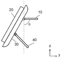
- FIG. 1B is a side view of the display device.
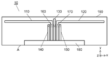
- FIG. 2 is a diagram illustrating a configuration of the antenna device.
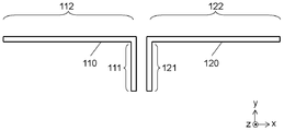
- FIG. 3 is a diagram showing the configuration of the first monopole antenna and the second monopole antenna.
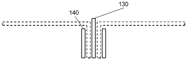
- FIG. 4 is a diagram showing the configuration of the first monopole antenna and the second monopole antenna.
- FIG. 5 is a diagram illustrating a configuration of the power feeding unit.
- FIG. 6 is a diagram showing the configuration of the third monopole antenna and the fourth monopole antenna.
- FIG. 7A is a diagram showing a radiation pattern of horizontal polarization of each antenna.
- FIG. 7B is a diagram showing a radiation pattern of horizontal polarization of each antenna.
- FIG. 7C is a diagram showing a radiation pattern of horizontal polarization of each antenna.
- FIG. 7D is a diagram showing a radiation pattern of horizontal polarization of each antenna.
- a display device having an antenna device according to an embodiment will be described with reference to the drawings.
- FIG. 1A is a perspective view illustrating an appearance of the display device 1.
- FIG. 1B is a side view of the display device 1.
- the display device 1 includes an antenna device 10, an LCD (Liquid Crystal Display) 20 as a display, a main body 30 containing various electric circuits, and a support member 40.
- the horizontal direction of the image display screen of the LCD 20 is the x axis
- the vertical direction of the display device 1 is the z axis
- the direction orthogonal to the x axis and the z axis is the y axis.
- the right direction of the image display surface of the LCD 20 in the front view is the positive direction of the x axis
- the left direction of the image display surface in the front view is the negative direction of the x axis.
- the upward direction of the display device 1 is defined as a positive direction of the z axis
- the downward direction of the vertical direction is defined as a negative direction of the z axis.
- the direction of the image display surface side of the LCD 20 is a negative y-axis direction
- the direction opposite to the image display surface is a positive y-axis direction.
- the LCD 20 has an image display surface in the negative direction of the y axis, and displays an image.
- the LCD 20 has a metal frame (not shown) that surrounds from the back side of the image display surface.
- the LCD 20 is located on the front side of the main body 30.
- the LCD 20 is an example of a display.
- an organic EL display or the like may be used.
- the main body 30 has an exterior casing made of a resin material.
- the main body 30 has an electric circuit board or the like (not shown) having a tuner circuit for receiving terrestrial digital broadcasting in an exterior casing.
- the main body 30 transmits an electric signal received by the antenna device 10 to a tuner circuit (not shown) and takes out desired video data.
- the main body 30 sends the extracted video data to the LCD 20 and causes the LCD 20 to display an image.
- the main body 30 includes a heat radiating metal member (not shown) for reducing heat generated in a power supply circuit, an audio circuit, a recording device, a reproducing device, an electric circuit board, and the like inside the outer casing. Have.
- the support member 40 is mainly made of a resin material.
- the support member 40 is rotatably fixed to the main body 30.
- the support member 40 supports the LCD 20 and the main body 30 so as to stand upright.
- the support member 40 includes a power feeding unit and an antenna inside. Details of the support member 40 will be described later.
- the antenna device 10 includes a plurality of antennas on a single base material and has a substantially rectangular plate shape.
- the antenna device 10 includes a power feeding unit to which a power feeding end of each antenna is connected at one end side of a rectangular shape.
- a support end A (see FIG. 2) on the side where the power feeding unit is provided is attached to the back surface of the main body 30.
- the antenna device 10 is rotatably attached to the back side of the LCD 20.
- the antenna device 10 is rotatably attached to the back surface of the main body 30. More specifically, the antenna device 10 can be rotated in the yz plane with the support portion as a fulcrum. Thus, the viewer can adjust the orientation of the antenna device 10 as appropriate.
- the LCD 20 has the image display surface facing away from the antenna device 10.
- ⁇ is an inclination angle in the yz plane with respect to the vertical direction.
- FIG. 2 is a diagram illustrating a configuration of the antenna device 10.
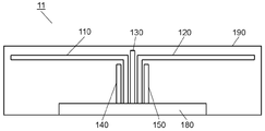
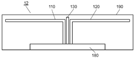
- the first monopole antenna 110, the second monopole antenna 120, the first parasitic element 130, the second parasitic element 140, and the third parasitic element 150 are made of acrylic resin or the like. It is formed by a predetermined pattern of metal such as copper on a flat insulating substrate 190.
- the antenna device 10 includes a power feeding unit 180 that is a first power feeding unit at an end of the insulating base material 190. Each of the first monopole antenna 110 and the second monopole antenna 120 is connected to the power feeding unit 180 at each power feeding end.
- the power supply ends of the antennas 110 and 120 and the terminals of the power supply unit 180 may be connected by a spring or the like.
- the power feeding end of each antenna and the terminal of the power feeding unit 180 may be connected by a spring or the like.
- the widths of the conductor patterns constituting the first monopole antenna 110, the second monopole antenna 120, the first parasitic element 130, the second parasitic element 140, and the third parasitic element 150 are: It is 3 mm and has a constant width.
- the antenna device 10 includes a jumper resistor 160 that connects ends of the first parasitic element 130 and the second parasitic element 140. Further, the antenna device 10 includes a jumper resistor 170 that connects ends of the first parasitic element 130 and the third parasitic element 150. These jumper resistors 160 and 170 are zero ohm chip resistors for conducting parasitic elements. Jumper resistors 160 and 170 are not connected to first monopole antenna 110 and second monopole antenna 120.
- the jumper resistors 160 and 170 are provided to insulate and straddle the first monopole antenna 110 and the second monopole antenna 120.
- the jumper resistors 160 and 170 are formed with the first monopole antenna 110, the second monopole antenna 120, the first parasitic element 130, the second parasitic element 140, and the third parasitic element 150 in the base material 190. It is attached by soldering etc. to the surface opposite to the surface.
- the jumper resistors 160 and 170 are examples of the first connection member and the second connection member, respectively.
- it may be a metal wire or a metal foil tape.
- any member that conducts between the parasitic elements may be used.
- the first monopole antenna 110, the second monopole antenna 120, the first parasitic element 130, the second parasitic element 140, and the third parasitic element 150 are, for example, printed metal patterns. It can be formed by attaching a metal film, attaching a metal wire, or etching a metal.
- the base material 190 is made of, for example, an acrylic material, and in the present embodiment, the outer shape of the base material 190 is a substantially rectangular flat plate shape of 218 mm ⁇ 55 mm, and has a shape having a recess where the power feeding unit 180 is located. .
- the power feeding unit 180 may be provided integrally with the base material 190.
- FIG. 3 is a diagram showing a detailed configuration of the first monopole antenna 110 and the second monopole antenna 120.
- the first monopole antenna 110 extends from a feeding end connected to the feeding unit 180 to a first portion 111 extending in the y-axis direction and from the first portion 111 to bend in the negative x-axis direction.
- the second portion 112 is configured.
- the second monopole antenna 120 includes a first part 121 extending in the y-axis direction from a power supply end connected to the power supply unit 180, and a second part extending from the first part 121 by bending in the positive x-axis direction. 2 parts 122.
- the first portion 111 of the first monopole antenna 110 extends in the short direction (first direction) of the substrate 190 from the power supply end connected to the power supply unit 180.
- the first portion 121 of the second monopole antenna 120 extends in the short direction (first direction) of the base material 190 from the power supply end connected to the power supply unit 180.
- “extending in the short direction” or “extending in the longitudinal direction” indicates a direction in which each element mainly extends, and includes a case where the element is partially bent.
- the first portion 111 of the first monopole antenna 110 and the first portion 121 of the second monopole antenna 120 extend so as to face each other.
- the first portion 111 and the second portion 112 are orthogonal to each other, and in the second monopole antenna 120, the first portion 121 and the second portion 122 are orthogonal to each other.
- the first part 111 of the first monopole antenna 110 and the first part 121 of the second monopole antenna 120 are arranged in parallel.
- the dimension of the first portion 111 of the first monopole antenna 110 is 45 mm.
- the dimension of the first portion 121 of the second monopole antenna 120 is 45 mm.
- the second portion 112 of the first monopole antenna 110 is bent by 90 degrees in the negative direction of the x axis at the end of the first portion 111 of the first monopole antenna 110 opposite to the power feeding portion 180 and extends 100 mm. Exist.
- the first monopole antenna 110 includes a first portion 111 extending in the same direction from a feeding end connected to the feeding portion 180, and a second portion 112 extending separately from the first portion 111 on the left and right. And have.
- the second portion 122 of the second monopole antenna 120 is bent at 90 degrees in the positive direction of the x-axis at the end of the first portion 121 of the second monopole antenna 120 opposite to the power feeding portion 180 and extends 100 mm. Exist.
- the second monopole antenna 120 includes a first portion 121 extending in the same direction from a feeding end connected to the feeding portion 180 and a second portion 122 extending separately from the first portion 121 on the left and right sides. And have.
- the first monopole antenna 110 and the second monopole antenna 120 are antennas that use the terrestrial digital broadcast band (473 MHz to 767 MHz) as a desired use band.
- the first parasitic element 130, the second parasitic element 140, and the third parasitic element 150 run in parallel with the first portion 111 of the first monopole antenna 110 and the first portion 121 of the second monopole antenna 120. Is provided on the substrate 190.
- the first parasitic element 130 extends in the short direction (first direction) of the base material 190 from the ground end connected to the ground layer of the power feeding unit 180.
- First parasitic element 130 is arranged to extend between first portion 111 of first monopole antenna 110 and first portion 121 of second monopole antenna 120.
- the first parasitic element 130 extends 45 mm from the power supply unit 180 in the positive direction of the y-axis.
- the second parasitic element 140 extends in the short direction (first direction) of the base 190 from the ground end connected to the ground layer of the power feeding unit 180.
- the second parasitic element 140 is formed on the base 190 so that the first portion 111 of the first monopole antenna 110 is sandwiched between the second parasitic element 140 and the first parasitic element 130.
- the second parasitic element 140 extends from the power supply unit 180 by 35 mm in the positive direction of the y-axis.
- the third parasitic element 150 extends in the short direction (first direction) of the base 190 from the ground end connected to the ground layer of the power feeding unit 180.
- the third parasitic element 150 is formed on the base 190 so that the first portion 121 of the second monopole antenna 120 is sandwiched between the third parasitic element 150 and the first parasitic element 130.
- the third parasitic element 150 extends from the power supply unit 180 by 35 mm in the positive direction of the y-axis.
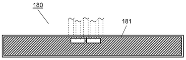
- FIG. 5 is a schematic diagram illustrating a configuration of the power feeding unit 180.
- the power feeding unit 180 is formed of a single two-layer substrate having a conductive layer and a dielectric layer.
- the power feeding unit 180 is mounted with a matching circuit and an LNA (Low Noise Amplifier) circuit (not shown).
- the power feeding unit 180 is connected to the power feeding ends of the first monopole antenna 110 and the second monopole antenna 120.
- a ground area 181 (ground layer) to which the first parasitic element 130, the second parasitic element 140, and the third parasitic element 150 are connected is formed in the conductive layer.
- the ground area 181 is a conductive pattern that provides an electrical ground potential for the first monopole antenna 110 and the second monopole antenna 120.
- the ground area 181 extends in the direction in which the second portion 112 of the first monopole antenna 110 and the second portion 122 of the second monopole antenna 120 extend (in the present embodiment, the x-axis direction). .
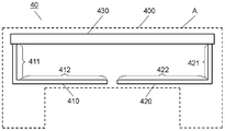
- the support member 40 includes a third monopole antenna 410, a fourth monopole antenna 420, and a power feeding unit 430 that is a second power feeding unit inside an exterior 400 made of a resin material.
- the exterior 400 is indicated by a dotted line
- the built-in third monopole antenna 410, the fourth monopole antenna 420, and the power feeding unit 430 are indicated by a solid line.
- Each of the third monopole antenna 410 and the fourth monopole antenna 420 has first portions 411 and 421 that extend in the same direction from the feeding end connected to the feeding portion 430.
- Each of the third monopole antenna 410 and the fourth monopole antenna 420 includes second portions 412 and 422 extending from the first portions 411 and 412 in directions facing each other.
- the third monopole antenna 410 is bent in a positive direction of 90 degrees x-axis from the end of the first portion 411 and the first portion 411 extending 45 mm from the power feeding portion 430, The second portion 412 extends 100 mm.
- the fourth monopole antenna 420 includes a first part 421 extending 45 mm from the power feeding part 430 and a second part extending 100 mm from the end of the first part 421 by bending 90 degrees in the negative x-axis direction. 422.
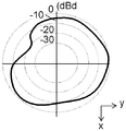
- FIG. 7A shows the radiation pattern of the first monopole antenna 110.
- the first monopole antenna 110 has a high gain in the back direction of the display device 1 (positive direction of the y axis) and in the ⁇ 45 ° direction of the display device 1.
- ⁇ is an angle shown in FIG. 7A, and is an angle when the negative direction of the x axis is set as a reference (0 degree) in the xy plane.
- FIG. 7B shows the radiation pattern of the second monopole antenna 120.
- the second monopole antenna 120 has a high gain in the back direction of the display device 1 (positive direction of the y axis) and in the ⁇ 135 ° direction of the display device 1.
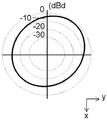
- FIG. 7C shows the radiation pattern of the third monopole antenna 410.
- the third monopole antenna 410 has a high gain in the ⁇ 315 ° direction of the display device 1.
- FIG. 7D shows the radiation pattern of the fourth monopole antenna 420.
- the fourth monopole antenna 420 has a high gain in the ⁇ 225 ° direction of the display device 1.
- the first monopole antenna 110 and the second monopole antenna 120 have strong directivities in different directions. Therefore, a reduction in gain due to the coupling between the first monopole antenna 110 and the second monopole antenna 120 can be suppressed.
- the first monopole antenna 110, the second monopole antenna 120, the third monopole antenna 410, and the fourth monopole antenna 420 have strong directivities in different directions. ing. Therefore, the coupling between the first monopole antenna 110, the second monopole antenna 120, the third monopole antenna 410, and the fourth monopole antenna 420 can be reduced. As a result, a reduction in gain can be suppressed.
- the antenna device 10 includes the jumper resistors 160 and 170, the second parasitic element 140, and the third parasitic element 150, but these are not necessarily essential elements.
- the jumper resistors 160, 170 shown in FIG. 2 may be omitted.
- the first parasitic element 130 it is possible to suppress a reduction in gain due to the coupling of the first monopole antenna 110 and the second monopole antenna 50.
- the reduction in gain can be further suppressed when the jumper resistors 160 and 170, the second parasitic element 140, and the third parasitic element 150 are provided.
- the antenna device 10 included in the display device 1 includes the power feeding unit 180, the first monopole antenna 110, the second monopole antenna 120, the first parasitic element 130, And a base material 190 on which is formed.
- Each of the first monopole antenna 110 and the second monopole antenna 120 includes first portions 111 and 121 extending in the same direction from a power feeding end connected to the power feeding unit 180.
- each of the first monopole antenna 110 and the second monopole antenna 120 includes second portions 112 and 122 extending separately from the first portions 111 and 121 on the left and right sides.
- the first parasitic element 130 is disposed between the first portion 111 of the first monopole antenna 110 and the first portion 121 of the second monopole antenna 120.
- the second portions 112 and 122 can be divided into left and right after a predetermined distance from the power supply unit 180 side, and the distance from the ground existing on the power supply unit 180 side. Can be secured and the coupling can be reduced.
- the presence of the first parasitic element 130 allows the first monopole antenna 110 and the second monopole antenna 120, which are antennas in the same frequency band, to be loosely coupled to each other and disposed in the vicinity.
- the antenna device 10 includes a second parasitic element 140 formed on the base material 190 so as to sandwich the first portion 111 of the first monopole antenna 110 between the first parasitic element 130 and a first parasitic element. And a third parasitic element 150 formed on the base 190 so as to sandwich the first portion 121 of the second monopole antenna 120 between the feeder element 130 and the feeder element 130.
- the antenna device 10 electrically connects the jumper resistor 160 that electrically connects the first parasitic element 130 and the second parasitic element 140, and the first parasitic element 130 and the third parasitic element 150. And a jumper resistor 170 to be connected.
- each parasitic element can be stabilized, and the first portions 111 and 121 can be further reduced from being coupled with other portions. As a result, the gain of the antenna device 10 can be further increased.
- the power feeding unit 180 includes a ground layer 181 formed on the substrate.
- the ground layer 181 extends in a direction in which the second portion 112 of the first monopole antenna 110 and the second portion 122 of the second monopole antenna 120 extend.
- the technique disclosed here is suitable for increasing the sensitivity of a device having a plurality of antenna devices.
Landscapes
- Details Of Aerials (AREA)
- Support Of Aerials (AREA)
- Variable-Direction Aerials And Aerial Arrays (AREA)
Abstract
Description
10,11,12 アンテナ装置
20 LCD
30 本体
40 支持部材
110 第1ダイポールアンテナ
111 第1部分
112 第2部分
120 第2ダイポールアンテナ
121 第1部分
122 第2部分
130 第1無給電素子
140 第2無給電素子
150 第3無給電素子
160,170 ジャンパ抵抗
180 給電部
190 基材
400 外装
410 第3モノポールアンテナ
411 第1部分
412 第2部分
420 第4モノポールアンテナ
421 第1部分
422 第2部分
430 給電部
Claims (6)
- 絶縁性の基材に第1モノポールアンテナと第2モノポールアンテナとを配置したアンテナ装置であって、
前記第1モノポールアンテナおよび前記第2モノポールアンテナは、給電部に接続される給電端から同じ方向に延在する第1部分と、前記第1部分からそれぞれ左右に分かれて延在する第2部分とを有し、
かつ前記第1モノポールアンテナの第1部分と前記第2モノポールアンテナの第1部分との間に、無給電素子を配置した
アンテナ装置。 - 前記第1モノポールアンテナの第1部分および前記第2モノポールアンテナの第1部分は、前記第1モノポールアンテナと前記第2モノポールアンテナの第1部分の間に配置した前記無給電素子と、前記第1部分の外側に配置された別の無給電素子とにより挟まれた構成である
請求項1記載のアンテナ装置。 - 前記第1モノポールアンテナと前記第2モノポールアンテナの第1部分の間に配置した前記無給電素子と、前記第1部分の外側に配置された別の無給電素子とは、接続部材により電気的に接続した
請求項2記載のアンテナ装置。 - 絶縁性の基材に第1モノポールアンテナと第2モノポールアンテナとを配置したアンテナ装置と、前記アンテナ装置で受けた電波を電気信号に変換する電気回路を有する本体と、前記本体からの前記電気信号を受けて画像を表示するディスプレイとを備えた表示装置であって、
前記アンテナ装置の第1モノポールアンテナおよび前記第2モノポールアンテナは、給電部に接続される給電端から同じ方向に延在する第1部分と、前記第1部分からそれぞれ左右に分かれて延在する第2部分とを有し、
かつ前記第1モノポールアンテナの第1部分と前記第2モノポールアンテナの第1部分との間に、無給電素子を配置した
表示装置。 - 前記第1モノポールアンテナの第1部分および前記第2モノポールアンテナの第1部分は、前記第1モノポールアンテナと前記第2モノポールアンテナの第1部分の間に配置した前記無給電素子と、前記第1部分の外側に配置された別の無給電素子とにより挟まれた構成である
請求項4記載の表示装置。 - 前記第1モノポールアンテナと前記第2モノポールアンテナの第1部分の間に配置した前記無給電素子と、前記第1部分の外側に配置された別の無給電素子とは、接続部材により電気的に接続した
請求項5記載の表示装置。
Priority Applications (3)
| Application Number | Priority Date | Filing Date | Title |
|---|---|---|---|
| JP2012523523A JP5423895B2 (ja) | 2010-07-06 | 2011-07-05 | アンテナ装置および表示装置 |
| CN201180018391.4A CN102834971B (zh) | 2010-07-06 | 2011-07-05 | 天线装置及显示装置 |
| US13/520,040 US8766871B2 (en) | 2010-07-06 | 2011-07-05 | Antenna apparatus and display apparatus |
Applications Claiming Priority (2)
| Application Number | Priority Date | Filing Date | Title |
|---|---|---|---|
| JP2010153603 | 2010-07-06 | ||
| JP2010-153603 | 2010-07-06 |
Publications (1)
| Publication Number | Publication Date |
|---|---|
| WO2012004977A1 true WO2012004977A1 (ja) | 2012-01-12 |
Family
ID=45440967
Family Applications (1)
| Application Number | Title | Priority Date | Filing Date |
|---|---|---|---|
| PCT/JP2011/003823 Ceased WO2012004977A1 (ja) | 2010-07-06 | 2011-07-05 | アンテナ装置および表示装置 |
Country Status (4)
| Country | Link |
|---|---|
| US (1) | US8766871B2 (ja) |
| JP (1) | JP5423895B2 (ja) |
| CN (1) | CN102834971B (ja) |
| WO (1) | WO2012004977A1 (ja) |
Cited By (1)
| Publication number | Priority date | Publication date | Assignee | Title |
|---|---|---|---|---|
| JP2014204153A (ja) * | 2013-04-01 | 2014-10-27 | 三菱電機株式会社 | アンテナ取り付け構造 |
Families Citing this family (8)
| Publication number | Priority date | Publication date | Assignee | Title |
|---|---|---|---|---|
| US9865914B2 (en) * | 2013-01-31 | 2018-01-09 | Hewlett-Packard Development Company, L.P. | Multi-position display deck and antenna |
| TWI682587B (zh) * | 2018-12-19 | 2020-01-11 | 國立交通大學 | 微型高增益場型可重構天線 |
| US11200388B2 (en) * | 2019-07-12 | 2021-12-14 | Zebra Technologies Corporation | System and method for accurately reading radio-frequency identification tags at a bioptic barcode reader |
| USD1011324S1 (en) * | 2021-04-02 | 2024-01-16 | Space Exploration Technologies Corp. | Antenna apparatus |
| USD1024036S1 (en) * | 2021-04-02 | 2024-04-23 | Space Exploration Technologies Corp. | Antenna apparatus |
| USD989750S1 (en) * | 2021-04-02 | 2023-06-20 | Space Exploration Technologies Corp. | Antenna apparatus |
| USD1099084S1 (en) | 2023-05-03 | 2025-10-21 | Space Exploration Technologies Corp. | Antenna apparatus |
| USD1065161S1 (en) | 2023-05-03 | 2025-03-04 | Space Exploration Technologies Corp. | Antenna apparatus |
Citations (3)
| Publication number | Priority date | Publication date | Assignee | Title |
|---|---|---|---|---|
| JP2000174529A (ja) * | 1998-12-07 | 2000-06-23 | Asahi Glass Co Ltd | 自動車用高周波ガラスアンテナ |
| JP2005347882A (ja) * | 2004-05-31 | 2005-12-15 | Toshiba Corp | 放送受信装置 |
| JP2010098411A (ja) * | 2008-10-15 | 2010-04-30 | Panasonic Corp | ダイバーシティアンテナ装置と、これを用いた電子機器 |
Family Cites Families (8)
| Publication number | Priority date | Publication date | Assignee | Title |
|---|---|---|---|---|
| JP3805772B2 (ja) | 2004-01-13 | 2006-08-09 | 株式会社東芝 | アンテナ装置及び携帯無線通信装置 |
| EP1814195A4 (en) | 2004-10-01 | 2009-07-15 | Panasonic Corp | ANTENNA DEVICE AND WIRELESS TERMINAL WITH ANTENNA DEVICE |
| JP4345719B2 (ja) * | 2005-06-30 | 2009-10-14 | ソニー株式会社 | アンテナ装置及び無線通信装置 |
| JP2007281906A (ja) | 2006-04-07 | 2007-10-25 | Sony Corp | アンテナおよびテレビ受信機 |
| JP4915215B2 (ja) | 2006-11-14 | 2012-04-11 | ソニー株式会社 | テレビジョン装置 |
| JP4904302B2 (ja) | 2008-03-28 | 2012-03-28 | 古河電気工業株式会社 | 車載用アンテナおよび複合アンテナ |
| US8890763B2 (en) * | 2011-02-21 | 2014-11-18 | Funai Electric Co., Ltd. | Multiantenna unit and communication apparatus |
| US9444129B2 (en) * | 2011-05-13 | 2016-09-13 | Funai Electric Co., Ltd. | Multi-band compatible multi-antenna device and communication equipment |
-
2011
- 2011-07-05 WO PCT/JP2011/003823 patent/WO2012004977A1/ja not_active Ceased
- 2011-07-05 US US13/520,040 patent/US8766871B2/en not_active Expired - Fee Related
- 2011-07-05 CN CN201180018391.4A patent/CN102834971B/zh not_active Expired - Fee Related
- 2011-07-05 JP JP2012523523A patent/JP5423895B2/ja not_active Expired - Fee Related
Patent Citations (3)
| Publication number | Priority date | Publication date | Assignee | Title |
|---|---|---|---|---|
| JP2000174529A (ja) * | 1998-12-07 | 2000-06-23 | Asahi Glass Co Ltd | 自動車用高周波ガラスアンテナ |
| JP2005347882A (ja) * | 2004-05-31 | 2005-12-15 | Toshiba Corp | 放送受信装置 |
| JP2010098411A (ja) * | 2008-10-15 | 2010-04-30 | Panasonic Corp | ダイバーシティアンテナ装置と、これを用いた電子機器 |
Cited By (1)
| Publication number | Priority date | Publication date | Assignee | Title |
|---|---|---|---|---|
| JP2014204153A (ja) * | 2013-04-01 | 2014-10-27 | 三菱電機株式会社 | アンテナ取り付け構造 |
Also Published As
| Publication number | Publication date |
|---|---|
| CN102834971B (zh) | 2015-09-23 |
| US8766871B2 (en) | 2014-07-01 |
| JP5423895B2 (ja) | 2014-02-19 |
| US20120280887A1 (en) | 2012-11-08 |
| CN102834971A (zh) | 2012-12-19 |
| JPWO2012004977A1 (ja) | 2013-09-02 |
Similar Documents
| Publication | Publication Date | Title |
|---|---|---|
| JP5423895B2 (ja) | アンテナ装置および表示装置 | |
| JP5454683B2 (ja) | アンテナ装置および表示装置 | |
| JP5506940B2 (ja) | アンテナ装置 | |
| US9865915B2 (en) | Electronic device with diverse antenna array having soldered connections | |
| US20080158088A1 (en) | Antenna for gps | |
| JP2008193299A (ja) | 逆f型アンテナ | |
| US8816927B2 (en) | Antenna unit, and electronic apparatus including the same | |
| JP5374649B2 (ja) | アンテナ装置 | |
| JP5391271B2 (ja) | 無線受信機器 | |
| KR102145399B1 (ko) | 무선 시스템용 안테나 | |
| TWI524592B (zh) | 新穎平面無線電天線模組 | |
| CN2935501Y (zh) | 微带缝隙天线 | |
| CN101483269B (zh) | 应用于无线广域网的天线 | |
| JP5609855B2 (ja) | 受信装置 | |
| CN109980351A (zh) | 多信号馈入表面粘着式的信号收发模块 | |
| CN117748169A (zh) | 电子设备 | |
| JPWO2006001049A1 (ja) | 無線タグ装置 | |
| JP2003347829A (ja) | アンテナ | |
| JP2011182359A (ja) | 受信装置 | |
| JP2008078764A (ja) | アンテナ装置 |
Legal Events
| Date | Code | Title | Description |
|---|---|---|---|
| WWE | Wipo information: entry into national phase |
Ref document number: 201180018391.4 Country of ref document: CN |
|
| 121 | Ep: the epo has been informed by wipo that ep was designated in this application |
Ref document number: 11803315 Country of ref document: EP Kind code of ref document: A1 |
|
| WWE | Wipo information: entry into national phase |
Ref document number: 2012523523 Country of ref document: JP |
|
| WWE | Wipo information: entry into national phase |
Ref document number: 13520040 Country of ref document: US |
|
| NENP | Non-entry into the national phase |
Ref country code: DE |
|
| 122 | Ep: pct application non-entry in european phase |
Ref document number: 11803315 Country of ref document: EP Kind code of ref document: A1 |