WO2012002132A1 - インクジェットヘッド - Google Patents
インクジェットヘッド Download PDFInfo
- Publication number
- WO2012002132A1 WO2012002132A1 PCT/JP2011/063329 JP2011063329W WO2012002132A1 WO 2012002132 A1 WO2012002132 A1 WO 2012002132A1 JP 2011063329 W JP2011063329 W JP 2011063329W WO 2012002132 A1 WO2012002132 A1 WO 2012002132A1
- Authority
- WO
- WIPO (PCT)
- Prior art keywords
- wiring
- row
- nozzles
- vias
- arrangement region
- Prior art date
- Legal status (The legal status is an assumption and is not a legal conclusion. Google has not performed a legal analysis and makes no representation as to the accuracy of the status listed.)
- Ceased
Links
Images








Classifications
-
- B—PERFORMING OPERATIONS; TRANSPORTING
- B41—PRINTING; LINING MACHINES; TYPEWRITERS; STAMPS
- B41J—TYPEWRITERS; SELECTIVE PRINTING MECHANISMS, i.e. MECHANISMS PRINTING OTHERWISE THAN FROM A FORME; CORRECTION OF TYPOGRAPHICAL ERRORS
- B41J2/00—Typewriters or selective printing mechanisms characterised by the printing or marking process for which they are designed
- B41J2/005—Typewriters or selective printing mechanisms characterised by the printing or marking process for which they are designed characterised by bringing liquid or particles selectively into contact with a printing material
- B41J2/01—Ink jet
- B41J2/135—Nozzles
- B41J2/14—Structure thereof only for on-demand ink jet heads
- B41J2/14201—Structure of print heads with piezoelectric elements
-
- B—PERFORMING OPERATIONS; TRANSPORTING
- B41—PRINTING; LINING MACHINES; TYPEWRITERS; STAMPS
- B41J—TYPEWRITERS; SELECTIVE PRINTING MECHANISMS, i.e. MECHANISMS PRINTING OTHERWISE THAN FROM A FORME; CORRECTION OF TYPOGRAPHICAL ERRORS
- B41J2/00—Typewriters or selective printing mechanisms characterised by the printing or marking process for which they are designed
- B41J2/005—Typewriters or selective printing mechanisms characterised by the printing or marking process for which they are designed characterised by bringing liquid or particles selectively into contact with a printing material
- B41J2/01—Ink jet
- B41J2/015—Ink jet characterised by the jet generation process
- B41J2/04—Ink jet characterised by the jet generation process generating single droplets or particles on demand
- B41J2/045—Ink jet characterised by the jet generation process generating single droplets or particles on demand by pressure, e.g. electromechanical transducers
-
- B—PERFORMING OPERATIONS; TRANSPORTING
- B41—PRINTING; LINING MACHINES; TYPEWRITERS; STAMPS
- B41J—TYPEWRITERS; SELECTIVE PRINTING MECHANISMS, i.e. MECHANISMS PRINTING OTHERWISE THAN FROM A FORME; CORRECTION OF TYPOGRAPHICAL ERRORS
- B41J2/00—Typewriters or selective printing mechanisms characterised by the printing or marking process for which they are designed
- B41J2/005—Typewriters or selective printing mechanisms characterised by the printing or marking process for which they are designed characterised by bringing liquid or particles selectively into contact with a printing material
- B41J2/01—Ink jet
- B41J2/135—Nozzles
- B41J2/14—Structure thereof only for on-demand ink jet heads
- B41J2/14201—Structure of print heads with piezoelectric elements
- B41J2/14233—Structure of print heads with piezoelectric elements of film type, deformed by bending and disposed on a diaphragm
-
- B—PERFORMING OPERATIONS; TRANSPORTING
- B41—PRINTING; LINING MACHINES; TYPEWRITERS; STAMPS
- B41J—TYPEWRITERS; SELECTIVE PRINTING MECHANISMS, i.e. MECHANISMS PRINTING OTHERWISE THAN FROM A FORME; CORRECTION OF TYPOGRAPHICAL ERRORS
- B41J2/00—Typewriters or selective printing mechanisms characterised by the printing or marking process for which they are designed
- B41J2/005—Typewriters or selective printing mechanisms characterised by the printing or marking process for which they are designed characterised by bringing liquid or particles selectively into contact with a printing material
- B41J2/01—Ink jet
- B41J2/135—Nozzles
- B41J2/14—Structure thereof only for on-demand ink jet heads
- B41J2002/14459—Matrix arrangement of the pressure chambers
-
- B—PERFORMING OPERATIONS; TRANSPORTING
- B41—PRINTING; LINING MACHINES; TYPEWRITERS; STAMPS
- B41J—TYPEWRITERS; SELECTIVE PRINTING MECHANISMS, i.e. MECHANISMS PRINTING OTHERWISE THAN FROM A FORME; CORRECTION OF TYPOGRAPHICAL ERRORS
- B41J2/00—Typewriters or selective printing mechanisms characterised by the printing or marking process for which they are designed
- B41J2/005—Typewriters or selective printing mechanisms characterised by the printing or marking process for which they are designed characterised by bringing liquid or particles selectively into contact with a printing material
- B41J2/01—Ink jet
- B41J2/135—Nozzles
- B41J2/14—Structure thereof only for on-demand ink jet heads
- B41J2002/14491—Electrical connection
-
- B—PERFORMING OPERATIONS; TRANSPORTING
- B41—PRINTING; LINING MACHINES; TYPEWRITERS; STAMPS
- B41J—TYPEWRITERS; SELECTIVE PRINTING MECHANISMS, i.e. MECHANISMS PRINTING OTHERWISE THAN FROM A FORME; CORRECTION OF TYPOGRAPHICAL ERRORS
- B41J2202/00—Embodiments of or processes related to ink-jet or thermal heads
- B41J2202/01—Embodiments of or processes related to ink-jet heads
- B41J2202/18—Electrical connection established using vias
Definitions
- the present invention relates to an ink jet head provided in an ink jet recording apparatus.
- an ink jet recording apparatus that records a desired image on a recording medium by ejecting ink droplets from nozzles of an ink jet head.
- This ink jet recording apparatus is used in a wide variety of applications, and types of inks and recording media suitable for each purpose can be used.
- An inkjet head includes a piezoelectric head that pressurizes ink in a pressure chamber using displacement of a piezoelectric element and ejects ink droplets from nozzles communicating with the pressure chamber.
- nozzles are arranged at high density in order to form a high-definition image.
- a set of nozzles and pressure chambers communicating with the nozzles is arranged two-dimensionally.
- FIG. 13A is a perspective view of the wiring substrate 200 of the inkjet head as seen from above and a perspective view of the head substrate 210 provided below the wiring substrate 200.
- FIG. 13B is a perspective view of the lower surface of the wiring substrate 200 of the inkjet head from the top surface side.
- the head substrate 210 is seen through.
- both a pressure chamber 202 and the like to be described later provided on the head substrate 210 below the wiring substrate 200 are seen through.
- FIG. 14 is a cross-sectional view of the wiring substrate 200 and the head substrate 210 of the inkjet head. As shown in FIG.
- a head substrate 210 of the inkjet head is provided with a plurality of nozzles 201, and a pressure chamber 202, an ink flow path 203, and a piezoelectric element 204 (see FIG. 14) corresponding to each nozzle 201.
- a wiring substrate 200 having a wiring 205 connected to the piezoelectric element 204 is provided above the piezoelectric element 204, and the wiring 205 is led to the upper surface of the wiring substrate 200 through a through via 206.
- the wiring 205 is connected to a wiring connection portion 207 provided outside the two-dimensional array region of the nozzle 201 and the pressure chamber 202.
- Each wiring 205 corresponding to each nozzle is connected to the wiring connecting portion 207 while avoiding the ink flow path 203.
- N / 2 wirings in each row are connected between adjacent ink flow paths (FIGS. 13A and 13B).
- N the number of nozzles per row
- the number of piezoelectric elements provided corresponding to each nozzle is also N.
- the wiring is drawn out on both left and right sides (upper and lower sides with respect to the paper surface of FIGS. 13A and 13B), as shown in FIG. 14, between the ink flow paths corresponding to the nozzles in the first row on the left side (FIGS. 13A and 13B).
- the wirings are arranged most densely (between AB), and the number thereof is N / 2. Thereafter, as the second row and the third row are advanced, the number of wirings passed between the ink flow paths is decreased one by one. As described above, although the method of dividing the wiring has a margin compared to the case where all the wirings corresponding to the nozzles in each row are drawn in the same direction, there is a sufficient margin for arranging the nozzles at high density. Do not mean.
- the present invention has been made to solve the above problems, and can effectively reduce the cost by effectively utilizing the space of the wiring board with a simple configuration, and can arrange the nozzles at a higher density.
- An object of the present invention is to provide an ink jet head capable of improving the reliability of wiring.
- a pair of individual nozzles and corresponding pressure chambers and actuators are arranged in a two-dimensional array,
- a wiring board having wiring individually connected corresponding to each actuator, through vias individually connected corresponding to each wiring, and ink flow paths for individually supplying ink corresponding to each pressure chamber
- the invention according to claim 2 is the ink jet head according to claim 1, N is an even number of 2 or more,
- the wiring connected to the through vias corresponding to the nozzles in the (N / 2) th row from the first row is drawn out of the arrangement region on the first row side, and (N / 2) + 1th row
- the wiring connected to the through via corresponding to the nozzle in the Nth row is drawn out of the arrangement region on the Nth row side,
- Through-vias corresponding to arbitrary a (1 ⁇ a ⁇ N / 2) nozzles from the first to (N / 2) th nozzles are provided outside the arrangement region, and the (N / 2) ) Of the nozzles from the + 1st row to the Nth row, through vias corresponding to arbitrary b (1 ⁇ b ⁇ N / 2) nozzles are provided outside the arrangement region.
- the invention according to claim 3 is the ink jet head according to claim 2,
- the through via corresponding to the a nozzles is provided outside the arrangement region on the first row side, and the through via corresponding to the b nozzles is provided outside the arrangement region on the Nth row side. It is characterized by being.
- the invention according to claim 4 is the ink jet head according to claim 2 or 3,
- the connection portion includes a first connection portion provided outside the arrangement region on the first row side on one surface of the wiring board and a second connection provided outside the arrangement region on the N-th row side.
- the wiring connected to the through vias corresponding to the nozzles from the first row to the (N / 2) th row is connected to the first connection portion,
- the wiring connected to the through vias corresponding to the nozzles in the (N / 2) + 1st to (N) th rows is connected to the second connection portion.
- the invention according to claim 5 is the inkjet head according to claim 4,
- the through vias corresponding to the a nozzles are arranged outside the first connection part with the first connection part between the arrangement region and the first via part,
- the through vias corresponding to the b nozzles are arranged outside the second connection portion with the second connection portion interposed between the through nozzle and the arrangement region.
- the invention according to claim 6 is the inkjet head according to any one of claims 1 to 5,
- the number of through vias provided in the arrangement area is equal to the number of through vias provided outside the arrangement area.
- the invention according to claim 7 is the inkjet head according to any one of claims 1 to 5,
- the number of through vias provided in the arrangement area is greater than the number of through vias provided outside the arrangement area.
- the invention according to claim 8 is the inkjet head according to any one of claims 1 to 7, On the surface of the wiring board opposite to the surface on which the connection portion is provided, a bonding member is provided in which a communication path for communicating the ink flow path with the pressure chamber is formed.
- the wiring connected to the through via outside the arrangement region is arranged at a position other than the joint portion between the wiring board and the joining member.
- the wiring connected to all the through vias is connected to the ink flow path. No need to pass between them.
- column with the densest wiring can be reduced, and a wiring width and the space
- the wiring can be concentrated on one surface of the wiring board through the through via, it is only necessary to provide the connection portion on one surface of the wiring board. This eliminates the need for a multilayer wiring board and eliminates the need to provide connection portions on both sides of the wiring board, thereby making it possible to reduce costs by effectively utilizing the space of the wiring board with a simple configuration.
- the second aspect of the present invention by drawing out all the wirings in the first row side and the Nth row side, it corresponds to the nozzles in the first row and the Nth row where the wiring is the densest.
- Wiring disposed between the ink flow paths can be reduced, and the wiring width and the interval between the wirings can be increased.
- each bundle of wirings divided into two directions can be divided into wirings connected to through vias in the wiring area and wirings connected to through vias outside the wiring area, the first column
- the wiring arranged between the ink flow paths corresponding to the nozzles in the Nth row can be further reduced, and the wiring width and the interval between the wirings can be further increased.
- the through vias provided outside the wiring region are arranged away from each other in the directions opposite to each other when viewed from the arrangement region of the first column side and the Nth column side. It can be used, and the wiring width and the interval between the wirings can be widened.
- the wiring drawn out to the first column side is connected to the first connection portion on the first column side, and the wiring drawn out to the Nth column side is connected to the second row on the Nth column side. Therefore, the distance from each through via to the connecting portion to be connected can be shortened, and the wiring can be shortened.
- the connecting portion is arranged between the two-dimensional arrangement region and the through via, the wiring can be connected to the connecting portion from both sides of the connecting portion.
- the wiring width around the connecting portion and the interval between the wirings can be widened, and the wiring space can be effectively used.
- the ink substrate for supplying ink to the pressure chamber is provided on the surface of the wiring board on the side where the piezoelectric element is provided, the wiring is connected to the ink. It is necessary to avoid the flow path, and the wiring space is also narrower than the other surface.
- the wiring connected to the through via provided outside the arrangement area is arranged on the surface provided with the ink flow path, the number of wirings on the surface provided with the ink flow path is set within the arrangement area. It is possible to reduce the number of wirings connected to the through via provided in the wiring. Thereby, the balance of the wiring width of the wiring of both surfaces of a wiring board and the space
- the wiring connected to the through via outside the arrangement region is arranged at a position other than the bonding portion between the wiring board and the bonding member, thereby joining the bonding member and the wiring board. A decrease in strength can be prevented.
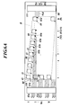
- FIG. 4 is an enlarged view of the periphery of a piezoelectric element in FIG. 3. It is the figure which showed the positional relationship of a pressure chamber, an ink flow path, and a piezoelectric element. It is a figure showing arrangement of a nozzle, a pressure chamber, a penetration via, the 2nd wiring, and a connection part in a 1st embodiment, and is a figure showing arrangement of wiring on the upper surface of a wiring board.
- FIG. 1 is a schematic diagram showing a main part of the ink jet recording apparatus 1.
- the ink jet recording apparatus 1 includes a transport unit 2 that transports the recording medium P in the direction of arrow Y (hereinafter referred to as the transport direction Y).
- the recording medium P in addition to paper and fabric, it is possible to use a plastic film or metal having no ink absorbability, and is not particularly limited.
- the paper here includes not only paper for exclusive use of an ink jet printer having ink absorptivity, but also coated paper, art paper, and plain paper having low ink absorptivity.
- An inkjet head 3 that ejects ink droplets D onto a recording medium P on the transport unit 2 is disposed above the transport unit 2.
- a plurality of nozzles 11 for ejecting ink droplets D are arranged in the X direction and the Y direction in the drawing (see FIG. 2).
- the transport unit 2 and the inkjet head 3 are connected to the control unit 5 and controlled by the control unit 5.
- FIG. 2 is a perspective view of the inkjet head 3.
- the inkjet head 3 includes a nozzle plate 20 having a plurality of nozzles 11 for discharging ink droplets D formed at the lower end thereof.
- FIG. 3 is a longitudinal sectional view of the inkjet head
- FIG. 4 is an enlarged view of the periphery of the piezoelectric element in FIG.
- the ink-jet head 3 connects the head substrate 150, the wiring substrate 80, and the head substrate 150 and the wiring substrate 80, which are configured by laminating three substrates of the nozzle plate 20, the intermediate plate 30, and the pressure chamber plate 40. And a member to be laminated.
- the inkjet head 3 includes a nozzle plate 20 as a nozzle substrate on which a plurality of nozzles 11 for ejecting ink are formed.
- the nozzle plate 20 is positioned at the lowermost layer of the inkjet head 3 when ink is ejected downward from the nozzles 11.
- the nozzle plate 20 uses silicon as a base material, and the ink flow path 12 and the nozzle 11 are formed by dry etching.
- the intermediate plate 30 is a substrate made of glass, and an ink flow path connecting an ink flow path 31 leading to the nozzle 11 and a pressure chamber 41 and an ink flow path 42 provided on the pressure chamber plate 40, which will be described later.
- a path 32 is formed.
- An example of a method for forming the ink flow paths 31 and 32 is a sand blast method.
- the intermediate plate 30 is joined to the nozzle plate 20.
- An example of the bonding method is anodic bonding.
- the anodic bonding is a method in which the intermediate plate 30 is heated (300 ° C. to 500 ° C.), a voltage is applied between the nozzle plate 20 and the intermediate plate 30, and both are bonded by electrostatic attraction.
- the ink flow path 31 is formed at a position communicating with the ink flow path 12 when the intermediate plate 30 is stacked on the nozzle plate 20.
- the pressure chamber plate 40 is formed of a silicon substrate, and includes a pressure chamber 41 provided individually corresponding to each nozzle 11 and an inlet (throttle channel) 42 serving as an ink channel to the pressure chamber 41. Is formed.
- An example of a method for forming the pressure chamber 41 and the inlet 42 is dry etching.
- the pressure chamber plate 40 is bonded to the intermediate plate 30 that is a glass substrate by anodic bonding. At the time of joining, the pressure chamber 41 is aligned so as to communicate with the ink flow path 31 formed in the intermediate plate 30.
- the anodic bonding here is also the same method as the bonding of the intermediate plate 30.
- a pressure chamber 41 for storing ink ejected from the nozzles 11 is formed so as to penetrate in the thickness direction of the pressure chamber plate 40.
- an inlet (throttle channel) 42 that becomes an ink flow path to the pressure chamber 41 is formed so as to penetrate in the thickness direction of the pressure chamber plate 40.
- the inlet 42 is formed to be thinner than other ink flow paths by dry etching.
- the flow path resistance is defined by the inlet 42, and desired discharge characteristics (droplet diameter, discharge frequency, etc.) can be realized.
- the pressure chamber 41 and the inlet 42 are formed so as to be independent from each other in the pressure chamber plate 40, but the ink flow path 32 formed in the intermediate plate 30 when the pressure chamber plate 40 is stacked on the intermediate plate 30. It is communicated via. Accordingly, the ink is stored in the pressure chamber 41 through the inlet 42 and the ink flow path 32.
- the pressure chamber plate 40 is provided with a diaphragm 50.
- the diaphragm 50 is provided on the pressure chamber plate 40 so as to cover the opening of the pressure chamber 41 while avoiding the inlet 42. That is, the diaphragm 50 constitutes one wall portion of the pressure chamber 41.
- the diaphragm 50 is formed in a thin plate shape, and can change the pressure in the pressure chamber 41 by displacement (elastic deformation) in the thickness direction.
- FIG. 5 is a diagram showing a positional relationship among the pressure chamber 41, an ink flow path 88 described later, and the piezoelectric element 60.
- the diaphragm 50 is provided with a piezoelectric element 60 at a position facing the pressure chamber 41 across the diaphragm 50.
- the piezoelectric element 60 is an actuator made of PZT (lead zirconate titanate), and is provided individually for each pressure chamber 41 and applies a force for causing the ink in the pressure chamber 41 to be ejected from the nozzle 11.
- PZT lead zirconate titanate
- the piezoelectric element 60 is sandwiched between two electrodes 61 and 62 from the upper surface side and the lower surface side, and the electrode 61 on the lower surface side is provided on the diaphragm 50.
- the piezoelectric element 60 and the electrodes 61 and 62 are provided by patterning the diaphragm 50 by a method such as etching.
- a voltage is applied to the electrodes 61 and 62, the piezoelectric element 60 sandwiched between the electrodes 61 and 62 is bent and deformed, and the diaphragm 50 is also bent and deformed by the deformation of the piezoelectric element 60.
- the ink in the pressure chamber 41 is ejected from the nozzle as an ink droplet D (see FIG. 1).
- the diaphragm 50 is provided with a joining member 70 as an insulating layer, and the pressure chamber plate 40 is joined to the wiring board 80 via the joining member 70.
- the joining member 70 is made of resin, and communicates with an inlet 42 formed on the pressure chamber plate 40 and an ink channel 88 provided on the wiring board 80, which will be described later. It is comprised as a columnar member in which 72 (communication path) was formed.
- a space 71 that accommodates the piezoelectric element 60 and the electrodes 61 and 62 is formed in the bonding member 70 so as to penetrate the bonding member 70 in the thickness direction at a position facing the pressure chamber 41 across the diaphragm 50. Yes.
- a plurality of spaces 71 are formed so as to accommodate each piezoelectric element 60 individually.
- an ink flow path 72 is formed so as to penetrate the bonding member 70 in the thickness direction independently of the space 71.
- the bonding member 70 exists in almost the entire area in the area outside the two-dimensional arrangement area where the nozzles 11, the pressure chambers 41, the piezoelectric elements 60, etc. are arranged in a two-dimensional arrangement in the inkjet head 3.
- the chamber plate 40 and the wiring board 80 are joined.
- a wiring substrate 80 is laminated and bonded to the bonding member 70.
- the wiring board 80 uses silicon as a base material.
- Two layers of insulating layers 82 and 83 of silicon oxide are formed on the lower surface of the wiring board 80, and an insulating layer 84 of silicon oxide is also formed on the upper surface.
- the insulating layer 83 located below is in contact with and joined to the upper surface of the joining member 70.
- an electrode through hole (through hole) 86 through which the through via 85 (through electrode) passes in order to apply a driving voltage to the electrode 62 to displace the piezoelectric element 60 is provided in the thickness direction of the wiring substrate 80. Is formed.
- first wiring 87 One end of a first wiring 87 extending in the horizontal direction is connected to the lower end of the through via 85, and the other end of the first wiring 87 is provided on the electrode 62 on the upper surface of the piezoelectric element 60.
- the stud bump 63 is connected via the solder 64 exposed in the space 71.
- the first wiring 87 is protected by being sandwiched between two insulating layers 82 and 83 on the lower surface of the wiring board 80.
- the first wiring 87 is made of a highly conductive material such as aluminum or copper.
- the insulating layers 82, 83, 84 provided on the upper and lower surfaces of the wiring board 80 are provided to insulate the first wiring 87 and the second wiring 91 from the wiring board 80 itself.
- a second wiring 91 is provided on the upper surface of the wiring substrate 80 with an insulating layer 84 interposed therebetween, and a protective layer 90 is provided on the second wiring 91.
- the second wiring 91 is formed from a highly conductive material such as aluminum or copper, for example.
- the protective layer 90 is a photosensitive adhesive that laminates and joins members constituting the wall surface of the upper common ink chamber 100 and is a protective layer that protects the second wiring 91.
- the second wiring 91 extends in the horizontal direction, and has one end connected to the upper end of the through via 85 and the other end connected to the connection portions 110 and 111 (see FIGS. 6A and 6B) to the drive circuit.
- the wirings 87 and 91 are individually connected corresponding to the piezoelectric element 60, and the through via 85 connects the first wiring 87 and the second wiring 91.
- the connection parts 110 and 111 are provided on the upper surface side of the wiring board 80.
- an ink flow path 88 for guiding ink to the pressure chamber 41 is formed so as to penetrate in the thickness direction of the wiring board 80.
- the ink flow path 88 is formed so as to communicate with the ink flow path 72 when the wiring substrate 80 is laminated on the bonding member 70.
- a protective layer 90 as an insulating layer is provided on the upper surface of the wiring board 80 (opposite the surface on which the bonding member 70 is provided), and protects the second wiring 91 provided on the upper surface of the wiring board 80. is doing.
- an ink channel 92 for guiding ink to the pressure chamber 41 is formed so as to penetrate in the thickness direction of the protective layer 90.
- the ink flow path 92 is formed so as to communicate with the ink flow path 88 formed in the wiring board 80 when the protective layer 90 is laminated on the wiring board 80.
- a common ink chamber 100 is provided on the upper surface of the wiring substrate 80 via a protective layer 90. Members constituting the wall surface of the common ink chamber 100 are joined to the wiring substrate 80 by a fixing means such as an adhesive.
- the common ink chamber 100 communicates with the pressure chamber 41 through the ink flow path in each layer.
- the common ink chamber 100 communicates with all the pressure chambers 41 via the ink flow path, and is formed so that ink can be supplied to all the pressure chambers 41.
- FIG. 6A and FIG. 6B are drawn sideways due to space limitations, the following description will be made from the right side of the paper surface of FIG. 6A and FIG. 6B.
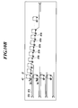
- 6A and 6B are diagrams for explaining the layout of wiring.
- FIG. 6A is a diagram showing the layout of wiring on the upper surface of the wiring board 80
- FIG. 6B is a diagram showing the layout of wiring on the lower surface of the wiring board 80. It is.
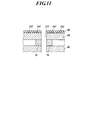
- FIG. 7 is a cross-sectional view of the wiring substrate 80 and the head substrate 150 for explaining the arrangement of each wiring.
- N nozzles 11 are arranged in parallel in the X direction (N is an even number of 2 or more) in the lowermost layer of the head substrate 150 to form a nozzle row. It is arranged in parallel in the Y direction over M rows (M is an integer of 2 or more). That is, M ⁇ N nozzles 11 are formed. Further, each nozzle row is arranged so that its position is slightly shifted in the Y direction.
- the nozzles 11 are arranged in a two-dimensional array, and the pressure chambers 41 and the piezoelectric elements 60 provided at positions corresponding to the nozzles 11 are also arranged in a two-dimensional array.
- an arrangement area in which the nozzles 11 and the like are arranged in a two-dimensional array is referred to as a two-dimensional arrangement area R.
- the first connecting portion 110 is provided at one end portion in the X direction of the inkjet head 3 (left side in FIGS. 6A and 6B), and the second connecting portion 111 is the other end portion in the X direction of the inkjet head 3 (see FIG. 6). 6A and the right side of FIG. 6B).
- the two connecting portions 110 and 111 are provided outside the two-dimensional arrangement region R in which the nozzle 11, the pressure chamber 41, and the piezoelectric elements 60 are arranged in a two-dimensional array.
- the leftmost nozzle row (first connection portion side) is the first row
- the rightmost (second connection portion side) nozzle row is the Nth row
- the uppermost nozzle row is the uppermost nozzle row.
- the wirings 87 and 91 corresponding to the nozzles 11 from the first column to the (N / 2) th column are connected to the first connection unit 110.
- the wires 87 and 91 corresponding to the nozzles 11 from the (N / 2) + 1th row to the Nth row are connected to the second connecting portion 111.
- N 16 nozzle rows
- the wirings 87 and 91 of the left half nozzle row (first to eighth rows) are connected to the first connecting portion 110, and the right half nozzle row (first row)
- the wirings 87 and 91 in the ninth column to the sixteenth column are connected to the second connection unit 111.
- the through vias 85 corresponding to the nozzles 11 from the first row to the eighth row are two-dimensionally arranged on the first row side of the nozzle row. It is provided outside the region R. More specifically, the through vias 85a corresponding to the nozzles 11 from the first row to the fourth row sandwich the first connection portion 110 with the two-dimensional arrangement region R in the wiring board 80, and the first via It is arranged outside the connection part 110.
- the through vias 85 corresponding to the nozzles 11 from the first row to the eighth row are provided in the two-dimensional arrangement region R. . More specifically, the through vias 85 b corresponding to the nozzles 11 in the fifth to eighth rows are arranged above the piezoelectric elements 60 in the wiring board 80.
- the ink flow paths 88 corresponding to the nozzles 11 from the fifth row to the eighth row are closer to the first connecting portion 110 (in other words, the first row side) than the through via 85 b corresponding to each nozzle 11.
- the ink flow path 88 is disposed on the left side of the through via 85b, in other words, the ink flow path 88 is disposed between the through via 85b and the first connection portion 110.
- the first wires 87 a corresponding to the nozzles 11 from the first row to the fourth row are arranged on the lower surface of the wiring board 80.
- the first wiring 87a has one end connected to the piezoelectric element 60 and the other end connected to the lower end of the through via 85a.
- the second wiring 91 a corresponding to the nozzles 11 from the first row to the fourth row is disposed on the upper surface of the wiring board 80.
- One end of the second wiring 91a is connected to the upper end of the through via 85a, and the other end is connected to the first connection portion 110 from the outside of the first connection portion 110 with respect to the two-dimensional arrangement region R. Yes.
- the wiring from the first column to the fourth column is drawn out of the two-dimensional arrangement region R from the piezoelectric element 60 toward the first connecting portion 110 outside the two-dimensional arrangement region R (in other words, the first column side). Then, it is folded back by the through via 85 a and connected to the first connection part 110.
- the first wiring 87a corresponding to the nozzles 11 from the first column to the fourth column in the first row includes the joining member 70 corresponding to the nozzle 11 in the first row and the joining member 70 corresponding to the nozzle 11 in the second row. Between the two terminals (between AB in FIG. 6B).
- the wiring corresponding to the nozzles in the other rows from the second row to the (M ⁇ 1) th row is also connected to the first connection portion 110 through the bonding members 70 adjacent to the lower side.
- the wiring corresponding to the nozzles in the Mth row is connected to the first connecting portion 110 through a region adjacent to the lower side. That is, the first wiring 87 a connected to the through via 85 a on the lower surface of the wiring substrate 80 is disposed at a position other than the joint portion between the lower surface side of the wiring substrate 80 and the bonding member 70.
- the through vias 85 corresponding to the nozzles 11 from the first row to the eighth row are within the two-dimensional arrangement region R. Is provided. More specifically, the through vias 85 b corresponding to the nozzles 11 in the fifth to eighth rows are arranged above the piezoelectric elements 60 in the wiring board 80.
- the first wiring 87 b corresponding to the nozzles 11 from the fifth row to the eighth row is disposed on the lower surface of the wiring board 80.
- the first wiring 87b has one end connected to the piezoelectric element 60 and the other end connected to the lower end of the through via 85b.
- the second wiring 91 b corresponding to the nozzles 11 from the fifth row to the eighth row is disposed on the upper surface of the wiring board 80.
- the second wiring 91 b has one end connected to the upper end of the through via 85 b and the other end connected to the first connection part 110.
- the wiring from the fifth row to the eighth row is guided to the upper surface of the wiring substrate 80 from the through via 85b above the piezoelectric element 60, and the first connection portion 110 (in other words, the first connection portion 110 outside the two-dimensional arrangement region R). It is drawn out of the two-dimensional arrangement region R toward the first row side and is connected to the first connection part 110.
- the second wiring 91b corresponding to the nozzles 11 from the fifth column to the eighth column of the first row has the ink flow path 88 corresponding to the nozzle 11 of the first row and the ink flow corresponding to the nozzle 11 of the second row. It is connected to the 1st connection part 110 through between the paths 88 (between AB of FIG. 6A).
- the wiring corresponding to the nozzles in the other rows from the second row to the (M ⁇ 1) th row is also connected to the first connecting portion 110 through the ink flow path 88 adjacent to the lower side.
- the wiring corresponding to the nozzles in the Mth row is connected to the first connecting portion 110 through a region adjacent to the lower side.
- the through vias 85 corresponding to the nozzles 11 from the 9th row to the 16th row are two-dimensionally arranged on the 16th row side of the nozzle row. It is provided outside the region R. More specifically, the through vias 85c corresponding to the nozzles 11 from the ninth row to the twelfth row are connected to the two-dimensional arrangement region R in the wiring board 80 with the second connection portion 111 interposed therebetween. It is arranged outside the connecting portion 111.
- the through vias 85 corresponding to the nozzles 11 from the 9th row to the 16th row are provided in the two-dimensional arrangement region R. . More specifically, the through vias 85 d corresponding to the nozzles 11 from the 13th row to the 16th row are arranged above the piezoelectric elements 60 in the wiring board 80. The through vias 85d corresponding to the nozzles 11 from the 13th row to the 16th row are closer to the second connecting portion 111 (in other words, the 16th row side) than the ink flow path 88 corresponding to each nozzle 11. Is arranged. 6A and 6B, the through via 85d is disposed on the right side of the ink flow path 88, in other words, the through via 85d is disposed between the ink flow path 88 and the second connection portion 111.
- the first wiring 87 c corresponding to the nozzles 11 from the ninth row to the twelfth row is disposed on the lower surface of the wiring board 80.
- the first wiring 87c has one end connected to the piezoelectric element 60 and the other end connected to the lower end of the through via 85c.
- the second wiring 91 c corresponding to the nozzles 11 from the ninth row to the twelfth row is disposed on the upper surface of the wiring board 80.
- the second wiring 91c has one end connected to the upper end of the through via 85c and the other end connected to the second connection portion 111 from the outside of the second connection portion 111 with respect to the two-dimensional arrangement region R. Yes.
- the wiring from the ninth column to the twelfth column is drawn out of the two-dimensional arrangement region R from the piezoelectric element 60 toward the second connection portion 111 outside the two-dimensional arrangement region R (in other words, the sixteenth column side). Then, it is folded back by the through via 85 c and connected to the second connection portion 111.
- the first wiring 87c corresponding to the nozzles 11 from the ninth column to the twelfth column of the first row includes the joining member 70 corresponding to the nozzle 11 of the first row and the joining member 70 corresponding to the nozzle 11 of the second row.
- the CD in FIGS. 6A and 6B is connected to the second connecting portion 111.
- the wiring corresponding to the nozzles in the other rows from the second row to the (M ⁇ 1) th row is also connected to the second connection portion 111 through the bonding members 70 adjacent to the lower side.
- the wiring corresponding to the nozzles in the Mth row is connected to the second connection portion 111 through a region adjacent to the lower side. That is, the first wiring 87 c connected to the through via 85 c on the lower surface of the wiring substrate 80 is disposed at a position other than the joint portion between the lower surface side of the wiring substrate 80 and the bonding member 70.
- the through vias 85d corresponding to the nozzles 11 from the 13th row to the 16th row are in the two-dimensional arrangement region R. Is provided. More specifically, the through vias 85 d corresponding to the nozzles 11 from the 13th row to the 16th row are arranged above the piezoelectric elements 60 in the wiring board 80.
- the first wiring (not shown) corresponding to the nozzles 11 from the 13th row to the 16th row is arranged on the lower surface of the wiring board 80.
- the first wiring has one end connected to the piezoelectric element 60 and the other end connected to the lower end of the through via 85d.
- the second wiring 91 d corresponding to the nozzles 11 from the 13th row to the 16th row is arranged on the upper surface of the wiring board 80.
- the second wiring 91 d has one end connected to the upper end of the through via 85 d and the other end connected to the second connection portion 111.
- the wirings from the 13th row to the 16th row are led to the upper surface of the wiring board 80 from the through via 85d above the piezoelectric element 60, and the second connecting portion 111 (in other words, the first connecting portion 111 outside the two-dimensional arrangement region R). It is drawn out of the two-dimensional arrangement region R toward the 16th column side) and connected to the second connection portion 111.
- the second wiring 91d corresponding to the nozzles 11 from the 13th column to the 16th column of the first row has an ink flow path 88 corresponding to the nozzle 11 of the first row and an ink flow corresponding to the nozzle 11 of the second row.
- the second connection part 111 is connected to the path 88.
- the wiring corresponding to the nozzles in the other rows from the second row to the (M ⁇ 1) th row is also connected to the second connecting portion 111 through the ink flow path 88 adjacent to the lower side.
- the wiring corresponding to the nozzles in the Mth row is connected to the second connection portion 111 through a region adjacent to the lower side.
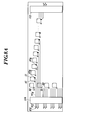
- FIGS. 8A and 8B are drawn in a horizontal direction due to space limitations, the following description will be made with reference to the paper surface of FIGS. 8A and 8B as viewed from the right side. 8A and 8B, the left side is the upper side, the right side is the lower side, the upper side is the right side, and the lower side is the left side.
- the through via 85f is provided outside the two-dimensional arrangement region R on the first row side of the nozzle row. More specifically, the through vias 85 f corresponding to the nozzles 11 in the first row, the third row, the fifth row, and the seventh row are connected to the two-dimensional arrangement region R in the wiring board 80 with the first connection portion 110. It is arrange
- the first wires 87 f corresponding to the nozzles 11 in the first row, the third row, the fifth row, and the seventh row are arranged on the lower surface of the wiring board 80.
- the first wiring 87f has one end connected to the piezoelectric element 60 and the other end connected to the lower end of the through via 85f.
- the second wiring 91 f corresponding to the nozzles 11 in the first, third, fifth, and seventh rows is disposed on the upper surface of the wiring board 80.
- One end of the second wiring 91f is connected to the upper end of the through via 85f, and the other end is connected to the first connection portion 110 from the outside of the first connection portion 110 with respect to the two-dimensional arrangement region R. Yes.
- the wirings in the first, third, fifth, and seventh rows are arranged in two lines from the piezoelectric element 60 toward the first connecting portion 110 (in other words, the first row side) outside the two-dimensional arrangement region R. It is pulled out of the dimension arrangement region R, folded back by a through via 85f, and connected to the first connection portion 110.
- the first wiring 87f corresponding to the nozzles 11 in the first column, the third column, the fifth column, and the seventh column of the first row includes the bonding member 70 corresponding to the nozzle 11 in the first row and the nozzle in the second row. 11 is connected to the first connecting portion 110 through the joint member 70 corresponding to the member 11 (between AB in FIG. 8B).
- the wiring corresponding to the nozzles in the other rows from the second row to the (M ⁇ 1) th row is also connected to the first connection portion 110 through the bonding members 70 adjacent to the lower side.
- the wiring corresponding to the nozzles in the Mth row is connected to the first connecting portion 110 through a region adjacent to the lower side. That is, the first wiring 87 f connected to the through via 85 f on the lower surface of the wiring substrate 80 is disposed at a position other than the joint portion between the lower surface side of the wiring substrate 80 and the bonding member 70.
- the through vias 85 corresponding to the nozzles 11 from the first row to the eighth row are two-dimensionally arranged regions. It is provided in R. More specifically, the through vias 85 g corresponding to the nozzles 11 in the second row, the fourth row, the sixth row, and the eighth row are disposed above the piezoelectric elements 60 in the wiring board 80.
- the first wiring (not shown) corresponding to the nozzles 11 in the second row, the fourth row, the sixth row, and the eighth row is arranged on the lower surface of the wiring board 80. Yes.
- the first wiring has one end connected to the piezoelectric element 60 and the other end connected to the lower end of the through via 85g.
- the second wiring 91 g corresponding to the nozzles 11 in the second row, the fourth row, the sixth row, and the eighth row is disposed on the upper surface of the wiring board 80.
- the second wiring 91g has one end connected to the upper end of the through via 85g and the other end connected to the first connecting portion 110.
- connection portion 110 (in other words, the first row side) is drawn out of the two-dimensional arrangement region R and connected to the first connection portion 110.
- the second wiring 91g corresponding to the nozzles 11 in the second column, the fourth column, the sixth column, and the eighth column in the first row is connected to the ink flow path 88 corresponding to the nozzle 11 in the first row and the second row. It is connected to the first connecting portion 110 through the ink flow path 88 corresponding to the nozzle 11 (between AB in FIG. 8A).
- the wiring corresponding to the nozzles in the other rows from the second row to the (M ⁇ 1) th row is also connected to the first connecting portion 110 through the ink flow path 88 adjacent to the lower side.
- the wiring corresponding to the nozzles in the Mth row is connected to the first connecting portion 110 through a region adjacent to the lower side.
- the wirings corresponding to the nozzles 11 from the ninth column to the sixteenth column are the wirings corresponding to the ninth column, the eleventh column, the thirteenth column, and the fifteenth column, similarly to the wirings from the first column to the eighth column.
- the second connection portion is connected to the second connection portion from the outside, and the wiring corresponding to the tenth column, the twelfth row, the fourteenth row, and the sixteenth row is connected to the second connection portion from the inner side than the second connection portion. Connected to the connection. Since the arrangement of the through vias and the wiring are the same as those in the first to eighth columns, the description thereof is omitted.
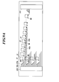
- FIGS. 9A and 9B are drawn sideways due to space limitations, the following description will be made with reference to the paper surface of FIGS. 9A and 9B as viewed from the right side. 9A and 9B, the left side is the upper side, the right side is the lower side, the upper side is the right side, and the lower side is the left side.
- the through vias 85h corresponding to the nozzles 11 from the first row to the fourth row are nozzles. It is provided outside the two-dimensional arrangement region R on the first column side of the column. More specifically, the through vias 85 h corresponding to the nozzles 11 from the first row to the fourth row are arranged between the two-dimensional arrangement region R and the first connection portion 110 in the wiring board 80.
- the first wiring 87 h corresponding to the nozzles 11 from the first row to the fourth row is disposed on the lower surface of the wiring board 80.
- the first wiring 87h has one end connected to the piezoelectric element 60 and the other end connected to the lower end of the through via 85h.
- the second wiring 91 h corresponding to the nozzles 11 from the first row to the fourth row is disposed on the upper surface of the wiring board 80.
- the second wiring 91h has one end connected to the upper end of the through via 85h and the other end connected to the two-dimensional arrangement region R from the inner side of the first connection part 110 to the first connection part 110. Yes.
- the wiring from the first row to the fourth row is two-dimensionally formed on the lower surface of the wiring board 80 from the piezoelectric element 60 toward the first connecting portion 110 (in other words, the first row side) outside the two-dimensional arrangement region R. It is pulled out of the arrangement region R, led to the upper surface of the wiring board 80 through the through via 85h, and connected to the first connection portion 110.
- the first wiring 87h corresponding to the nozzles 11 from the first column to the fourth column in the first row includes the joining member 70 corresponding to the nozzle 11 in the first row and the joining member 70 corresponding to the nozzle 11 in the second row.
- the wiring corresponding to the nozzles in the other rows from the second row to the (M ⁇ 1) th row is also connected to the first connection portion 110 through the bonding members 70 adjacent to the lower side.
- the wiring corresponding to the nozzles in the Mth row is connected to the first connecting portion 110 through a region adjacent to the lower side. That is, the first wiring 87 h connected to the through via 85 h on the lower surface of the wiring substrate 80 is disposed at a position other than the joint portion between the lower surface side of the wiring substrate 80 and the bonding member 70.
- the wirings corresponding to the nozzles 11 from the fifth row to the eighth row are the same as in the first embodiment.
- the wirings corresponding to the nozzles 11 from the ninth column to the sixteenth column are the same as the wirings from the first column to the eighth column, and the wirings corresponding to the ninth column to the twelfth column are changed from the first column to the fourth column. Since the wiring corresponding to the 13th to 16th columns is the same as the corresponding wiring corresponding to the 5th to 8th columns, the description thereof is omitted.
- the through vias 85j corresponding to the nozzles 11 from the first row to the third row are nozzles. It is provided outside the two-dimensional arrangement region R on the first column side of the column. More specifically, the through via 85j corresponding to the nozzles 11 from the first row to the third row has the first connection portion 110 sandwiched between the first via 110 and the two-dimensional arrangement region R in the wiring board 80. It is arranged outside the connection part 110.
- the first wires 87j corresponding to the nozzles 11 from the first row to the third row are arranged on the lower surface of the wiring board 80.
- the first wiring 87j has one end connected to the piezoelectric element 60 and the other end connected to the lower end of the through via 85j.
- the second wiring 91j corresponding to the nozzles 11 from the first row to the third row is arranged on the upper surface of the wiring board 80.
- the second wiring 91j has one end connected to the upper end of the through via 85j and the other end connected to the first connection portion 110 from the outside of the first connection portion 110 with respect to the two-dimensional arrangement region R. Yes.
- the wiring from the first row to the third row is two-dimensionally formed on the lower surface of the wiring board 80 from the piezoelectric element 60 toward the first connecting portion 110 outside the two-dimensional arrangement region R (in other words, the first row side). It is pulled out of the arrangement region R, led to the upper surface of the wiring board 80 through the through via 85j, and connected to the first connecting portion 110.
- the first wiring 87j corresponding to the nozzles 11 from the first column to the third column in the first row includes the joining member 70 corresponding to the nozzle 11 in the first row and the joining member 70 corresponding to the nozzle 11 in the second row. Between the two terminals (between AB in FIG. 10B).
- the wiring corresponding to the nozzles in the other rows from the second row to the (M ⁇ 1) th row is also connected to the first connection portion 110 through the bonding members 70 adjacent to the lower side.
- the wiring corresponding to the nozzles in the Mth row is connected to the first connecting portion 110 through a region adjacent to the lower side. That is, the first wiring 87 j connected to the through via 85 j on the lower surface of the wiring board 80 is disposed at a position other than the joint portion between the lower surface side of the wiring board 80 and the joining member 70.
- the wirings corresponding to the nozzles 11 from the fourth row to the eighth row are from the fifth row to the eighth row in the first embodiment.
- the wiring corresponding to the nozzle 11 is the same.
- the wirings corresponding to the nozzles 11 from the ninth column to the sixteenth column are the same as the wirings from the first column to the eighth column, and the wirings corresponding to the ninth column to the eleventh column are changed from the first column to the third column. Since the wiring corresponding to the 12th to 16th columns is the same as the wiring corresponding to the 4th to 8th columns, the description thereof is omitted.
- the through vias 85 corresponding to the nozzles 11 are arranged separately in the two-dimensional arrangement region R and outside the two-dimensional arrangement region R. It is not necessary to pass the wires 87 and 91 connected to 85 between the ink flow paths 88.
- the wirings 87 and 91 disposed between the ink flow paths 88 corresponding to the nozzles 11 in the first row and the 16th row where the wirings 87 and 91 are the densest can be greatly reduced. Can be widened.
- the nozzles 11 can be arranged with high density, and the reliability of the wirings 87 and 91 can be improved.
- the wirings 87 and 91 can be concentrated on one surface of the wiring board 80 via the through vias 85, the connection portions 110 and 111 need only be provided on one surface of the wiring board 80. This eliminates the need for the wiring board 80 to be multi-layered, and eliminates the need to provide the connection portions 110 and 111 on both sides of the wiring board 80, thereby reducing the cost by effectively utilizing the space of the wiring board 80 with a simple configuration. Can do.
- the wirings 87 and 91 arranged between the paths 88 can be reduced, and the wiring width and the spacing between the wirings can be increased.
- the bundle of the wirings 87 and 91 divided in two directions is connected to the through via in the two-dimensional arrangement region R and the wiring connected to the through via outside the two-dimensional arrangement region R. Since it can be divided, the wiring arranged between the ink flow paths 88 corresponding to the nozzles 11 in the first row and the 16th row can be further reduced, and the wiring width and the interval between the wires can be further widened.
- the wiring space can be effectively used by arranging the through vias provided outside the two-dimensional arrangement region R in the opposite directions as viewed from the two-dimensional arrangement region R of the first row side and the sixteenth row side. It is possible to increase the wiring width and the spacing between the wirings.
- the wiring drawn out to the first column side is connected to the first connection part 110 on the first column side, and the wiring drawn out to the 16th column side is connected to the second connection part 111 on the 16th column side. Therefore, the distance from each through via 85 to the connecting portions 110 and 111 to be connected can be shortened, and the wiring can be shortened.
- connection portions 110 and 111 are disposed between the two-dimensional arrangement region R and the through via, the wiring 91 can be connected to the connection portions 110 and 111 from both sides of the connection portions 110 and 111. . Thereby, the wiring width around the connection portions 110 and 111 and the interval between the wirings can be widened, and the wiring space can be effectively used.
- the number of through vias 85 inside and outside the two-dimensional arrangement region R is set to be the same, it is possible to make the same number of wirings arranged on the upper surface of the wiring board 80 and wiring arranged on the lower surface. As a result, only one wiring width and the interval between the wirings are not reduced, so that the wiring width and the interval between the wirings can be increased, and the wiring space can be used effectively.
- the bonding strength between the bonding member 70 and the wiring board 80 can be increased. A decrease can be prevented.
- an ink flow path 72 for supplying ink to the pressure chamber 41 is provided on the surface of the wiring substrate 80 on the side where the piezoelectric element 60 is provided (the lower surface of the wiring substrate). Since the joining member 70 is provided, the wiring 87 needs to be arranged avoiding the joining member 70, and the wiring space is also narrower than the other surface.
- the wiring 87j connected to the through via 85j provided outside the two-dimensional arrangement region R is arranged on the surface on which the joining member 70 is provided, the wiring on the surface on which the joining member 70 is provided. The number can be made smaller than the number of wirings connected to the through via 85b provided in the two-dimensional arrangement region R.
- the wiring space on the lower surface of the wiring board 80 is reduced by the amount of the joining member 70, it is preferable to arrange (N / 4) + n wirings on the upper surface and (N / 4) ⁇ n wirings on the lower surface.
- the wiring space can be used more effectively than in the case where the upper and lower surfaces of the wiring board 80 are the same number, which is preferable. Thereby, the balance of the wiring width of the wiring of both surfaces of the wiring board 80 and the space
- the interval between the wiring 161 adjacent to the ink flow path 151 and the ink flow path 151 is set between the wirings ( 161 and 162).
- the protective layer 90 formed on the upper surface of the wiring substrate 80 is missing or R is formed at the corner. Even in this case, the wiring 161 is hardly exposed to the outside. As a result, poor conduction of the wiring 161 can be prevented in advance. Therefore, when there is a margin in L / S, it is preferable to preferentially widen the interval between the wirings adjacent to the ink flow path.
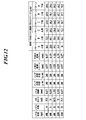
- FIG. 12 is a table comparing the space that can be secured per wiring when the nozzle density, the number of nozzle rows, and the wiring arrangement are changed.
- the nozzle density is 600 npi
- the number of nozzle rows N is 16
- the nozzle interval is 677 ⁇ m
- the inner diameter of the ink flow path is 100 ⁇ m
- the outer diameter of the ink flow path is 200 ⁇ m
- the ink in the first row A wiring pattern in which all 16 wirings are arranged between the flow paths pattern A in FIG.
- the space that can be secured per wiring is 36.1 ⁇ m, and L / S (line / space) is 18/18.
- the space that can be secured per wiring is 72.2 ⁇ m, and L / S (line / space) is 36/36.
- the space that can be secured per wiring is 144.3 ⁇ m on the upper surface side of the wiring substrate and 119.3 ⁇ m on the lower surface side, and L / S (line / space) is 72/72 on the upper surface side of the wiring substrate.
- the lower surface side is 59/59.
- the space that can be secured per wiring is 115.5 ⁇ m on the upper surface side and 159.1 ⁇ m on the lower surface side, and L / S (line / space) is 57/57 on the upper surface side of the wiring substrate.
- the lower surface side is 79/79.
- FIG. 12 shows the results of calculating the space that can be secured per wiring when the nozzle density and the number of nozzle rows are changed.
- the wiring pattern of the embodiment is the conventional wiring. It can be seen that the space that can be secured per wiring is larger than the pattern. Thus, the reliability of wiring can be improved by reducing the number of wirings passed between the ink flow paths.
- the present invention is not limited to the above-described embodiment, and design changes can be freely made without changing the essential part of the invention.
- the configuration when the number of connection portions is two is described, but the number of connection portions is increased to three or more, and the wiring is divided into three or more according to the number of connection portions. It is also possible.
- the wiring corresponding to the left nozzle row connected to the first connection portion and the wiring corresponding to the right nozzle row connected to the second connection portion are arranged in the same manner.
- the number of wires to be drawn out of the two-dimensional arrangement region may be different between the left and right nozzle rows.
- the ink jet head according to the present invention is useful for realizing high-definition image formation by arranging nozzles at high density.
Landscapes
- Particle Formation And Scattering Control In Inkjet Printers (AREA)
- Ink Jet (AREA)
Abstract
Description
インクジェットヘッドには、圧電素子の変位を利用して圧力室内のインクを加圧し、圧力室に連通するノズルからインク滴を吐出する圧電方式のヘッドがある。
このような圧電方式のヘッドにおいて、高精細な画像を形成するためにノズルを高密度に配置したものがあり、例えば、ノズルとこのノズルに連通した圧力室との組を2次元状に配列させたものが知られている(例えば、特許文献1参照)。
図14は、インクジェットヘッドの配線基板200及びヘッド基板210の断面図である。
図13Aに示すように、インクジェットヘッドのヘッド基板210には、複数のノズル201が設けられており、各ノズル201に対応して圧力室202、インク流路203、圧電素子204(図14参照)が設けられている。圧電素子204の上方には圧電素子204に接続される配線205を有する配線基板200が設けられており、この配線205は貫通ビア206を介して配線基板200の上面に導かれている。
ここで、配線205は、ノズル201や圧力室202の2次元配列領域外に設けられた配線接続部207に接続されている。各ノズルに対応する各配線205はインク流路203を避けて配線接続部207に接続されている。
例えば、1行あたりのノズルの数をN個であるとすると、各ノズルに対応して設けられている圧電素子の数もN個である。配線を左右両側(図13A及び図13Bの紙面に対して上下両側)に引き出した場合、図14に示すように、左側では第1列のノズルに対応するインク流路間(図13A及び図13BのAB間)が最も密に配線が配置され、その数はN/2本である。以降、第2列、第3列と進むにつれ、インク流路間に通される配線の数が1本ずつ減っていくことになる。
このように、配線を二分する方法は、各行のノズルに対応する全ての配線を同じ方向に引き出す場合に比べて余裕があるものの、ノズルを高密度に配置するためには、十分な余裕があるわけではない。
このような問題を解決するため、配線基板を複数層にわたって積層した多層配線基板を用いることも考えられるが、構造が複雑であり、インクジェットヘッドの厚みも増すため、軽量化やコスト低減が困難である。
また、特許文献1(図9A及び図9B参照)に示されているように、配線基板の両面に配線を分けて配置し、それぞれの面に設けられた駆動回路に接続することも考えられるが、配線基板の両面に駆動回路を設けると、インクジェットヘッドの製造が困難であり、インクジェットヘッドの厚みも増すため、軽量化やコスト低減が困難である。
インクを吐出する複数のノズルと、各ノズルに対応して個別に連通される圧力室と、各圧力室に対応して個別に設けられ、圧力室内のインクをノズルから吐出させるための力を付与するアクチュエータとを有し、個々のノズル及びこれに各々対応する圧力室とアクチュエータとの組が二次元配列状に配置され、
各アクチュエータに対応して個別に接続される配線と、各配線に対応して個別に接続される貫通ビアと、各圧力室に対応して個別にインクを供給するインク流路とを有する配線基板と、
前記個々のノズル及びこれに各々対応する圧力室とアクチュエータとの組が二次元配列状に配置された配置領域外に設けられ、各配線を駆動部に接続する接続部と、を備えるインクジェットヘッドにおいて、
ノズルは、M個(Mは2以上の整数)が直線状に並べられると共に、これがN列(Nは2以上の整数)にわたって設けられ、
N個のノズル列のうち、任意のn個(1≦n<N)のノズル列のノズルに対応する貫通ビアが前記配置領域内に設けられ、前記任意のn個以外のノズル列のノズルに対応する貫通ビアが前記配置領域外に設けられていることを特徴とする。
前記Nは2以上の偶数であり、
第1列から第(N/2)列のノズルに対応する貫通ビアに接続される配線は、第1列側の前記配置領域外に向けて引き出され、かつ、第(N/2)+1列から第N列のノズルに対応する貫通ビアに接続される配線は、第N列側の前記配置領域外に向けて引き出され、
第1列から第(N/2)列のノズルのうち、任意のa個(1≦a<N/2)のノズルに対応する貫通ビアが前記配置領域外に設けられ、第(N/2)+1列から第N列のノズルのうち、任意のb個(1≦b<N/2)のノズルに対応する貫通ビアが前記配置領域外に設けられていることを特徴とする。
前記a個のノズルに対応する貫通ビアは、第1列側の前記配置領域外に設けられ、前記b個のノズルに対応する貫通ビアは、第N列側の前記配置領域外に設けられていることを特徴とする。
前記接続部は、前記配線基板の一方の面における第1列側の前記配置領域外に設けられた第1の接続部と、第N列側の前記配置領域外に設けられた第2の接続部とを有し、
第1列から第(N/2)列のノズルに対応する貫通ビアに接続される配線は、前記第1の接続部に接続され、
第(N/2)+1列から第N列のノズルに対応する貫通ビアに接続される配線は、前記第2の接続部に接続されていることを特徴とする。
前記a個のノズルに対応する貫通ビアは、前記配置領域との間で前記第1の接続部を挟んで前記第1の接続部よりも外側に配置され、
前記b個のノズルに対応する貫通ビアは、前記配置領域との間で前記第2の接続部を挟んで前記第2の接続部よりも外側に配置されていることを特徴とする。
前記配置領域内に設けられた貫通ビアの数と前記配置領域外に設けられた貫通ビアの数とが等しいことを特徴とする。
前記配置領域内に設けられた貫通ビアの数は、前記配置領域外に設けられた貫通ビアの数よりも多いことを特徴とする。
前記配線基板における前記接続部が設けられている面と反対側の面には、前記インク流路を前記圧力室に連通させる連通路が形成された接合部材が設けられ、
前記配置領域外の貫通ビアに接続される配線は、前記配線基板と前記接合部材との接合部以外の位置に配置されていることを特徴とする。
また、貫通ビアを介して配線基板の一方の面に配線を集結させることができるので、接続部を配線基板の一方の面に設けるだけでよい。これにより、配線基板を多層にする必要もなく、接続部も配線基板の両面に設ける必要もなくなり、簡易な構成で配線基板のスペースを有効活用してコスト低減を図ることができる。
さらに、引き出す方向が二つに分けられたそれぞれの配線の束を、配線領域内の貫通ビアに接続する配線と配線領域外の貫通ビアに接続する配線とに分けることができるので、第1列及び第N列のノズルに対応するインク流路間に配置する配線をさらに減らすことができ、配線幅、配線同士の間隔をさらに広げることができる。
ここで、インク流路が設けられている面には、配置領域外に設けられた貫通ビアに接続する配線が配置されるので、インク流路が設けられている面の配線数を配置領域内に設けられた貫通ビアに接続する配線数よりも少なくすることができる。これにより、配線基板の両面の配線の配線幅、配線同士の間隔のバランスを良くすることができる。
[第1の実施形態]
<インクジェット記録装置>
図1は、インクジェット記録装置1の要部を示す模式図である。
図1に示すように、インクジェット記録装置1は、記録媒体Pを矢印Yの方向(以下、搬送方向Yという)へ搬送する搬送部2を備えている。記録媒体Pとしては、紙や布帛のほか、インク吸収性の無いプラスチックフィルムや金属類等を用いることが可能であり、特に限定されない。なお、ここでの紙とは、インク吸収性を有するインクジェットプリンタ専用紙は勿論のこと、インク吸収性の弱いコート紙やアート紙、及び普通紙を含むものである。
搬送部2の上方には、搬送部2上の記録媒体Pへインク滴Dを吐出するインクジェットヘッド3が配設されている。このインクジェットヘッド3には、インク滴Dを吐出する複数のノズル11が、図中のX方向及びY方向に配列されている(図2参照)。
搬送部2、インクジェットヘッド3は、制御部5に接続されており、この制御部5により制御される。
図2は、インクジェットヘッド3の斜視図である。
この図に示すように、インクジェットヘッド3はその下端にインク滴Dを吐出する複数のノズル11が形成されたノズルプレート20を備えている。
図3は、インクジェットヘッドの縦断面図であり、図4は、図3において圧電素子の周囲を拡大視した図である。
インクジェットヘッド3は、ノズルプレート20、中間プレート30、圧力室プレート40の3枚の基板が積層されて構成されているヘッド基板150と、配線基板80と、ヘッド基板150と配線基板80とを接続する部材とが積層されて構成されている。
図3,図4に示すように、インクジェットヘッド3は、インクを吐出する複数のノズル11が形成されたノズル基板としてのノズルプレート20を備えている。ノズルプレート20は、ノズル11からインクを下方に吐出する際にインクジェットヘッド3の最下層に位置する。ノズルプレート20は、シリコンを基材としており、ドライエッチングにより、インク流路12及びノズル11が形成されている。
中間プレート30は、ガラスで構成された基板であり、ノズル11へ通じるインク流路31と、後で説明する、圧力室プレート40に設けられた圧力室41とインク流路42を接続するインク流路32とが形成されている。インク流路31,32を形成する方法の一例としては、サンドブラスト法が挙げられる。
中間プレート30は、ノズルプレート20と接合されている。接合の方法としては、陽極接合を挙げることができる。ここで、陽極接合とは、中間プレート30を加熱(300℃~500℃)し、ノズルプレート20と中間プレート30との間に電圧を印加し、静電引力により両者を接合する方法である。陽極接合を用いることにより、両者を接着するための接着剤が不要となり、インク溶剤による耐久性劣化の恐れがなく、信頼性を高めることができる。
インク流路31は、中間プレート30をノズルプレート20に積層した際に、インク流路12に連通する位置に形成されている。
圧力室プレート40は、シリコン基板で構成されており、各ノズル11に対応して個別に設けられた圧力室41と、圧力室41へのインク流路となるインレット(絞り流路)42とが形成されている。圧力室41及びインレット42を形成する方法の一例としては、ドライエッチングが挙げられる。
圧力室プレート40は、ガラス基板である中間プレート30と陽極接合により接合されている。接合に際しては、圧力室41が中間プレート30に形成されたインク流路31と連通するように位置合わせがなされている。ここでの陽極接合も上記中間プレート30の接合と同じ方法である。圧力室プレート40には、ノズル11から吐出するインクを貯留する圧力室41が圧力室プレート40の厚さ方向に貫通するように形成されている。
圧力室41とインレット42は、圧力室プレート40においては互いに独立するように形成されているが、中間プレート30に圧力室プレート40を積層した際に、中間プレート30に形成されたインク流路32を介して連通される。従って、インクは、インレット42、インク流路32を通って圧力室41に貯留される。
圧力室プレート40には、振動板50が設けられている。振動板50は、インレット42を回避しつつ、圧力室41の開口を覆うように圧力室プレート40に設けられている。すなわち、振動板50は、圧力室41の一壁部を構成している。
振動板50は、薄板状に形成されており、厚さ方向への変位(弾性変形)により圧力室41内の圧力を変化させることができる。
図5は、圧力室41、後述するインク流路88、圧電素子60の位置関係を示した図である。
図4、図5に示すように、振動板50には、当該振動板50を挟んで圧力室41に対向する位置に圧電素子60が設けられている。
圧電素子60は、PZT(lead zirconate titanate)からなるアクチュエータであり、各圧力室41に対して個別に設けられ、圧力室41のインクをノズル11から吐出させるための力を付与するものである。
圧電素子60は、上面側及び下面側から二つの電極61,62により挟まれ、下面側の電極61が振動板50上に設けられている。圧電素子60及び電極61,62は、振動板50にエッチング等の方法でパターニング形成することにより設けられている。
電極61,62に電圧を印加すると、電極61,62に挟まれた圧電素子60が撓み変形し、圧電素子60の変形により振動板50も撓み変形する。この振動板50の動作により、圧力室41内のインクがノズルからインク滴D(図1参照)として吐出される。
振動板50には、絶縁層としての接合部材70が設けられており、接合部材70を介して、圧力室プレート40が配線基板80と接合されている。
接合部材70は、樹脂で形成されており、圧力室プレート40に形成されたインレット42と、後で説明する、配線基板80に設けられたインク流路88とを連通するようにしてインク流路72(連通路)が形成された柱状部材として構成されている。
接合部材70には、当該振動板50を挟んで圧力室41に対向する位置に圧電素子60及び電極61,62を収容する空間71が接合部材70の厚さ方向に貫通するように形成されている。空間71は、各圧電素子60を個別に収容するように複数形成されている。
接合部材70には、空間71とは独立してインク流路72が接合部材70の厚さ方向に貫通するように形成されている。
接合部材70は、インクジェットヘッド3における、ノズル11、圧力室41、圧電素子60等が二次元配列状に配置された二次元配置領域より外側の領域においては、領域のほぼ全面に存在し、圧力室プレート40と配線基板80を接合している。
接合部材70には、配線基板80が積層され、接合されている。配線基板80は、シリコンを基材としている。
配線基板80の下面には、2層の酸化シリコンの絶縁層82,83が形成され、上面には、同じく酸化シリコンの絶縁層84が形成されている。絶縁層82,83のうち、下方に位置する絶縁層83は、接合部材70の上面に当接し、接合されている。
配線基板80には、電極62に駆動電圧を印加して圧電素子60を変位させるために貫通ビア85(貫通電極)を通す電極用貫通孔(スルーホール)86が配線基板80の厚さ方向に形成されている。貫通ビア85の下端には、水平方向に延在する第1の配線87の一端が接続されており、この第1の配線87の他端には、圧電素子60上面の電極62に設けられたスタッドバンプ63が、空間71内に露出した半田64を介して接続されている。第1の配線87は、配線基板80の下面の2層の絶縁層82,83によって挟まれて保護されている。第1の配線87は、例えば、アルミニウムや銅等の導電性の高い材料から形成されている。
配線基板80の上面には、絶縁層84を挟んで第2の配線91が設けられ、第2の配線91には保護層90が設けられている。第2の配線91は、例えば、アルミニウムや銅等の導電性の高い材料から形成されている。
保護層90は、上方の共通インク室100の壁面を構成する部材を積層、接合する感光性の接着剤であるとともに、第2の配線91を保護する保護層となっている。第2の配線91は、水平方向に延在されて、一端が貫通ビア85の上端に接続されるとともに、他端が駆動回路への接続部110,111(図6A及び図6B参照)に接続されている。各配線87,91は、圧電素子60に対応して個別に接続され、貫通ビア85は、第1の配線87と第2の配線91を接続するものである。接続部110,111は、配線基板80の上面側に設けられている。
配線基板80には、インクを圧力室41に導くためのインク流路88が配線基板80の厚さ方向に貫通するように形成されている。インク流路88は、接合部材70に配線基板80を積層した際に、インク流路72に連通するように形成されている。
配線基板80の上面(接合部材70が設けられた面の反対側)には、絶縁層としての保護層90が設けられており、配線基板80上面に設けられている第2の配線91を保護している。
保護層90には、インクを圧力室41に導くためのインク流路92が保護層90の厚さ方向に貫通するように形成されている。インク流路92は、配線基板80に保護層90を積層した際に、配線基板80に形成されているインク流路88に連通するように形成されている。
配線基板80の上面には、保護層90を介して共通インク室100が設けられている。共通インク室100の壁面を構成する部材は、接着剤などの固定手段により配線基板80に接合されている。
共通インク室100は、各層におけるインク流路を介して圧力室41に連通されている。共通インク室100は、全ての圧力室41にインク流路を介して連通されており、全ての圧力室41にインクを供給することができるように形成されている。
ここで、各配線87,91、貫通ビア85、接続部110,111の配置について説明する。なお、図6A及び図6Bは紙面の制約上、横向きに描いているため、以下の説明においては、図6A及び図6Bの紙面に対して右側から見て説明する。すなわち、図6A及び図6Bの紙面を正面から見て、左側を上側、右側を下側、上側を右側、下側を左側として説明する。
図6A及び図6Bは、配線の配置を説明する図であり、このうち図6Aは配線基板80の上面の配線の配置を示す図、図6Bは配線基板80の下面の配線の配置を示す図である。なお、ノズルや圧力室は実際にはヘッド基板150の異なる層に設けられているものであるが、各構成の配置を明確にするために図6A及び図6Bではノズル11以外は全て実線で描いている。図7は、各配線の配置を説明する配線基板80及びヘッド基板150の断面図である。
図6A及び図6Bに示すように、ノズル11は、ヘッド基板150の最下層においてX方向にN個(Nは2以上の偶数)並設されてノズル列を構成しており、このノズル列がY方向にM行(Mは2以上の整数)にわたって並設されている。すなわち、ノズル11は、M×N個形成されている。また、各ノズル列は、Y方向に少しずつ位置がずれるように配置されている。すなわち、ノズル11は、二次元配列状に配置されており、各ノズル11に対応する位置に設けられている圧力室41、圧電素子60も二次元配列状に配置されていることになる。以下、ノズル11等が二次元配列状に配置されている配置領域を二次元配置領域Rとする。
第1列から第8列までのノズル11に対応する貫通ビア85のうち、第1列から第4列までのノズル11に対応する貫通ビア85aは、ノズル列の第1列側の二次元配置領域R外に設けられている。より詳細には、第1列から第4列までのノズル11に対応する貫通ビア85aは、配線基板80における二次元配置領域Rとの間で第1の接続部110を挟んで当該第1の接続部110よりも外側に配置されている。
第1列から第8列までのノズル11に対応する貫通ビア85のうち、第5列から第8列までのノズル11に対応する貫通ビア85bは、二次元配置領域R内に設けられている。より詳細には、第5列から第8列までのノズル11に対応する貫通ビア85bは、配線基板80における圧電素子60の上方に配置されている。
第5列から第8列までの各ノズル11に対応するインク流路88は、各ノズル11に対応する貫通ビア85bよりも第1の接続部110(言い換えると第1列側)に近い位置に配置されている。すなわち、図6A及び図6Bにおいては、インク流路88が貫通ビア85bよりも左側、言い換えると、インク流路88が貫通ビア85bと第1の接続部110との間に配置されている。
図6A、図7に示すように、第1列から第4列までのノズル11に対応する第2の配線91aは、配線基板80の上面に配置されている。第2の配線91aは、一端が貫通ビア85aの上端に接続され、他端が二次元配置領域Rに対して第1の接続部110よりも外側から当該第1の接続部110に接続されている。
すなわち、第1列から第4列までの配線は、圧電素子60から二次元配置領域R外の第1の接続部110(言い換えると第1列側)に向けて二次元配置領域R外に引き出され、貫通ビア85aで折り返されて第1の接続部110に接続されている。
すなわち、配線基板80の下面において貫通ビア85aに接続される第1の配線87aは、配線基板80の下面側と接合部材70との接合部以外の位置に配置されている。
図6A、図7に示すように、第5列から第8列までのノズル11に対応する第2の配線91bは、配線基板80の上面に配置されている。第2の配線91bは、一端が貫通ビア85bの上端に接続され、他端が第1の接続部110に接続されている。
すなわち、第5列から第8列までの配線は、圧電素子60の上方において貫通ビア85bから配線基板80の上面に導かれ、二次元配置領域R外の第1の接続部110(言い換えると第1列側)に向けて二次元配置領域R外に引き出されて第1の接続部110に接続されている。
第9列から第16列までのノズル11に対応する貫通ビア85のうち、第9列から第12列までのノズル11に対応する貫通ビア85cは、ノズル列の第16列側の二次元配置領域R外に設けられている。より詳細には、第9列から第12列までのノズル11に対応する貫通ビア85cは、配線基板80における二次元配置領域Rとの間で第2の接続部111を挟んで当該第2の接続部111よりも外側に配置されている。
第9列から第16列までのノズル11に対応する貫通ビア85のうち、第13列から第16列までのノズル11に対応する貫通ビア85dは、二次元配置領域R内に設けられている。より詳細には、第13列から第16列までのノズル11に対応する貫通ビア85dは、配線基板80における圧電素子60の上方に配置されている。
第13列から第16列までの各ノズル11に対応する貫通ビア85dは、各ノズル11に対応するインク流路88よりも第2の接続部111(言い換えると第16列側)に近い位置に配置されている。すなわち、図6A及び図6Bにおいては、貫通ビア85dがインク流路88よりも右側、言い換えると、貫通ビア85dがインク流路88と第2の接続部111との間に配置されている。
図6Aに示すように、第9列から第12列までのノズル11に対応する第2の配線91cは、配線基板80の上面に配置されている。第2の配線91cは、一端が貫通ビア85cの上端に接続され、他端が二次元配置領域Rに対して第2の接続部111よりも外側から当該第2の接続部111に接続されている。
すなわち、第9列から第12列までの配線は、圧電素子60から二次元配置領域R外の第2の接続部111(言い換えると第16列側)に向けて二次元配置領域R外に引き出され、貫通ビア85cで折り返されて第2の接続部111に接続されている。
すなわち、配線基板80の下面において貫通ビア85cに接続される第1の配線87cは、配線基板80の下面側と接合部材70との接合部以外の位置に配置されている。
図6Aに示すように、第13列から第16列までのノズル11に対応する第2の配線91dは、配線基板80の上面に配置されている。第2の配線91dは、一端が貫通ビア85dの上端に接続され、他端が第2の接続部111に接続されている。
すなわち、第13列から第16列までの配線は、圧電素子60の上方において貫通ビア85dから配線基板80の上面に導かれ、二次元配置領域R外の第2の接続部111(言い換えると第16列側)に向けて二次元配置領域R外に引き出されて第2の接続部111に接続されている。
次に、インクジェットヘッド3の第2の実施形態について説明する。第2の実施形態が第1の実施形態と異なる点は、配線基板における配線の配置であるため、以下では配線の配置について説明し、第1の実施形態と同じ部分は説明を省略する。なお、図8A及び図8Bは紙面の制約上、横向きに描いているため、以下の説明においては、図8A及び図8Bの紙面に対して右側から見て説明する。すなわち、図8A及び図8Bの紙面を正面から見て、左側を上側、右側を下側、上側を右側、下側を左側として説明する。
図8A及び図8Bに示すように、第1列から第8列までのノズル11に対応する貫通ビア85のうち、第1列、第3列、第5列、第7列のノズル11に対応する貫通ビア85fは、ノズル列の第1列側の二次元配置領域R外に設けられている。より詳細には、第1列、第3列、第5列、第7列のノズル11に対応する貫通ビア85fは、配線基板80における二次元配置領域Rとの間で第1の接続部110を挟んで当該第1の接続部110よりも外側に配置されている。
第1列、第3列、第5列、第7列のノズル11に対応する第2の配線91fは、配線基板80の上面に配置されている。第2の配線91fは、一端が貫通ビア85fの上端に接続され、他端が二次元配置領域Rに対して第1の接続部110よりも外側から当該第1の接続部110に接続されている。
すなわち、第1列、第3列、第5列、第7列の配線は、圧電素子60から二次元配置領域R外の第1の接続部110(言い換えると第1列側)に向けて二次元配置領域R外に引き出され、貫通ビア85fで折り返されて第1の接続部110に接続されている。
すなわち、配線基板80の下面において貫通ビア85fに接続される第1の配線87fは、配線基板80の下面側と接合部材70との接合部以外の位置に配置されている。
第2列、第4列、第6列、第8列のノズル11に対応する第2の配線91gは、配線基板80の上面に配置されている。第2の配線91gは、一端が貫通ビア85gの上端に接続され、他端が第1の接続部110に接続されている。
すなわち、第2列、第4列、第6列、第8列の配線は、圧電素子60の上方において貫通ビア85gから配線基板80の上面に導かれ、二次元配置領域R外の第1の接続部110(言い換えると第1列側)に向けて二次元配置領域R外に引き出されて第1の接続部110に接続されている。
次に、インクジェットヘッド3の第3の実施形態について説明する。第3の実施形態が第1の実施形態と異なる点は、配線基板における配線の配置であるため、以下では配線の配置について説明し、第1の実施形態と同じ部分は説明を省略する。なお、図9A及び図9Bは紙面の制約上、横向きに描いているため、以下の説明においては、図9A及び図9Bの紙面に対して右側から見て説明する。すなわち、図9A及び図9Bの紙面を正面から見て、左側を上側、右側を下側、上側を右側、下側を左側として説明する。
図9A及び図9Bに示すように、第1列から第8列までのノズル11に対応する貫通ビア85のうち、第1列から第4列までのノズル11に対応する貫通ビア85hは、ノズル列の第1列側の二次元配置領域R外に設けられている。より詳細には、第1列から第4列までのノズル11に対応する貫通ビア85hは、配線基板80における二次元配置領域Rと第1の接続部110との間に配置されている。貫通ビア85hをこのような位置に設けることで、接続部より外側に配線を配置することがないので、配線の配置領域を小さくすることができ、ひいてはインクジェットヘッドの小型化を図ることができる。
第1列から第4列までのノズル11に対応する第2の配線91hは、配線基板80の上面に配置されている。第2の配線91hは、一端が貫通ビア85hの上端に接続され、他端が二次元配置領域Rに対して第1の接続部110よりも内側から当該第1の接続部110に接続されている。
すなわち、第1列から第4列までの配線は、圧電素子60から二次元配置領域R外の第1の接続部110(言い換えると第1列側)に向けて配線基板80の下面で二次元配置領域R外に引き出され、貫通ビア85hで配線基板80の上面に導かれて第1の接続部110に接続されている。
すなわち、配線基板80の下面において貫通ビア85hに接続される第1の配線87hは、配線基板80の下面側と接合部材70との接合部以外の位置に配置されている。
なお、第9列から第16列までのノズル11に対応する配線も第1列から第8列の配線と同様、第9列から第12列に対応する配線が第1列から第4列に対応する配線と同様であり、第13列から第16列に対応する配線が第5列から第8列に対応する配線と同様であるため、説明を省略する。
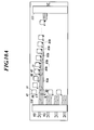
次に、インクジェットヘッド3の第4の実施形態について説明する。第4の実施形態が第1の実施形態と異なる点は、配線基板における配線の配置であるため、以下では配線の配置について説明し、第1の実施形態と同じ部分は説明を省略する。なお、図10A及び図10Bは紙面の制約上、横向きに描いているため、以下の説明においては、図10A及び図10Bの紙面に対して右側から見て説明する。すなわち、図10A及び図10Bの紙面を正面から見て、左側を上側、右側を下側、上側を右側、下側を左側として説明する。
図10A及び図10Bに示すように、第1列から第8列までのノズル11に対応する貫通ビア85のうち、第1列から第3列までのノズル11に対応する貫通ビア85jは、ノズル列の第1列側の二次元配置領域R外に設けられている。より詳細には、第1列から第3列までのノズル11に対応する貫通ビア85jは、配線基板80における二次元配置領域Rとの間で第1の接続部110を挟んで当該第1の接続部110よりも外側に配置されている。
第1列から第3列までのノズル11に対応する第2の配線91jは、配線基板80の上面に配置されている。第2の配線91jは、一端が貫通ビア85jの上端に接続され、他端が二次元配置領域Rに対して第1の接続部110よりも外側から当該第1の接続部110に接続されている。
すなわち、第1列から第3列までの配線は、圧電素子60から二次元配置領域R外の第1の接続部110(言い換えると第1列側)に向けて配線基板80の下面で二次元配置領域R外に引き出され、貫通ビア85jで配線基板80の上面に導かれて第1の接続部110に接続されている。
すなわち、配線基板80の下面において貫通ビア85jに接続される第1の配線87jは、配線基板80の下面側と接合部材70との接合部以外の位置に配置されている。
なお、第9列から第16列までのノズル11に対応する配線も第1列から第8列の配線と同様、第9列から第11列に対応する配線が第1列から第3列に対応する配線と同様であり、第12列から第16列に対応する配線が第4列から第8列に対応する配線と同様であるため、説明を省略する。
以上のように、上記実施形態によれば、ノズル11に対応する貫通ビア85は、二次元配置領域R内と二次元配置領域R外とに分けられて配置されているため、全ての貫通ビア85に接続された配線87,91をインク流路88間に通す必要がなくなる。本実施形態においては、左右の接続部に均等に配線を振り分けた場合、配線基板80の上面、下面共に最大N/4本の配線を通すだけで良くなる。
これにより、最も配線87,91が密になる第1列及び第16列のノズル11に対応するインク流路88間に配置する配線87,91を大幅に減らすことができ、配線幅、配線同士の間隔を広げることができる。よって、ノズル11を高密度に配置することができると共に、配線87,91の信頼性を向上させることができる。
また、貫通ビア85を介して配線基板80の一方の面に配線87,91を集結させることができるので、接続部110,111を配線基板80の一方の面に設けるだけでよい。これにより、配線基板80を多層にする必要もなく、接続部110,111も配線基板80の両面に設ける必要もなくなり、簡易な構成で配線基板80のスペースを有効活用してコスト低減を図ることができる。
さらに、引き出す方向が二つに分けられたそれぞれの配線87,91の束を、二次元配置領域R内の貫通ビアに接続する配線と二次元配置領域R外の貫通ビアに接続する配線とに分けることができるので、第1列及び第16列のノズル11に対応するインク流路88間に配置する配線をさらに減らすことができ、配線幅、配線同士の間隔をさらに広げることができる。
ここで、接合部材70が設けられている面には、二次元配置領域R外に設けられた貫通ビア85jに接続する配線87jが配置されるので、接合部材70が設けられている面の配線数を二次元配置領域R内に設けられた貫通ビア85bに接続する配線数よりも少なくすることができる。
すなわち、配線基板80の下面の方が、接合部材70の分だけ配線スペースが狭くなるため、配線を上面に(N/4)+n本、下面に(N/4)-n本配置する方が、配線基板80の上下面共に同じ本数にする場合に比べて配線スペースを有効に利用することができ、好ましい。
これにより、配線基板80の両面の配線の配線幅、配線同士の間隔のバランスを良くすることができる。
このように、インク流路151に隣接する配線161をインク流路151から大きく離すことにより、配線基板80の上面に形成される保護層90が欠けたり、角にRが形成されてしまっている場合であっても、配線161が外部に露出しにくくなる。これにより、配線161の導通不良を未然に防止することができる。
よって、L/Sに余裕がある場合には、インク流路に隣接する配線の間隔を優先的に広くとるようにすることが好ましい。
ここで、従来の配線の配置との比較を行うことにする。
図12は、ノズル密度、ノズル列数、配線の配置を変えた場合における1本の配線あたりに確保できるスペースを比較した表である。
図12の最上欄に示すように、ノズル密度が600npi、ノズル列数Nが16、ノズル間隔が677μm、インク流路の内径を100μm、インク流路の外径を200μmとし、第1列のインク流路間に16本全ての配線を配置した配線パターン(図12のパターンA)、第1列のインク流路間と第16列のインク流路間に8本ずつ配線を分けて配置した配線パターン(図12のパターンB)、第1列のインク流路間と第16列のインク流路間に8本ずつ配線を分けるとともに、8本の配線をさらに配線基板の上面と下面に4本ずつ配置した配線パターン(図12のパターンC:第1~第3の実施形態に対応)、第1列のインク流路間と第16列のインク流路間に8本ずつ配線を分けるとともに、8本の配線をさらに配線基板の上面に5本、下面に3本配置した配線パターン(図12のパターンD:第4の実施形態に対応)について、1本の配線あたりに確保できる配線スペースを算出した。
配線パターンBにおいては、配線1本あたりに確保できるスペースは、72.2μmとなり、L/S(ライン/スペース)は、36/36となる。
配線パターンCにおいては、配線1本あたりに確保できるスペースは、配線基板の上面側が144.3μm、下面側が119.3μmとなり、L/S(ライン/スペース)は、配線基板の上面側が72/72、下面側が59/59となる。
配線パターンDにおいては、配線1本あたりに確保できるスペースは、配線基板の上面側が115.5μm、下面側が159.1μmとなり、L/S(ライン/スペース)は、配線基板の上面側が57/57、下面側が79/79となる。
その他、ノズル密度、ノズル列数を変えた場合における1本の配線あたりに確保できるスペースを算出した結果を図12に示すが、いずれの条件においても、実施形態の配線パターンの方が従来の配線パターンよりも1本の配線あたりに確保できるスペースが大きいことがわかる。
このように、インク流路間に通す配線の数を少なくすることで、配線の信頼性を向上させることができる。
なお、図12のパターンDについて、ノズル列が32の場合は、第1列のインク流路間と第32列のインク流路間に16本ずつ配線を分けるとともに、16本の配線をさらに配線基板の上面に10本、下面に6本配置した配線パターンで計算している。
また、同様に、図12のパターンDについて、ノズル列が8の場合は、第1列のインク流路間と第8列のインク流路間に4本ずつ配線を分けるとともに、4本の配線をさらに配線基板の上面に3本、下面に1本配置した配線パターンで計算している。
なお、本発明は、上記実施形態に限られるものではなく、発明の本質的部分を変更しない範囲内で自由に設計変更が可能である。
例えば、上記実施形態においては、接続部を二つにしたときの構成について説明しているが、接続部の数を三つ以上に増やし、接続部の数に応じて配線を三つ以上に分けることも可能である。
また、上記実施形態においては、第1の接続部に接続する左側のノズル列に対応する配線と第2の接続部に接続する右側のノズル列に対応する配線とで同じ配置としたが、必ずしも同じにする必要はなく、二次元配置領域外に引き出す配線数を左右のノズル列で異なるようにしても良い。
11 ノズル
41 圧力室
60 圧電素子(アクチュエータ)
70 接合部材
72 インク流路(連通路)
80 配線基板
85 貫通ビア
87 第1の配線(配線)
88 インク流路
91 第2の配線(配線)
110 第1の接続部(接続部)
111 第2の接続部(接続部)
R 二次元配置領域(配置領域)
Claims (8)
- インクを吐出する複数のノズルと、各ノズルに対応して個別に連通される圧力室と、各圧力室に対応して個別に設けられ、圧力室内のインクをノズルから吐出させるための力を付与するアクチュエータとを有し、個々のノズル及びこれに各々対応する圧力室とアクチュエータとの組が二次元配列状に配置され、
各アクチュエータに対応して個別に接続される配線と、各配線に対応して個別に接続される貫通ビアと、各圧力室に対応して個別にインクを供給するインク流路とを有する配線基板と、
前記個々のノズル及びこれに各々対応する圧力室とアクチュエータとの組が二次元配列状に配置された配置領域外に設けられ、各配線を駆動部に接続する接続部と、を備えるインクジェットヘッドにおいて、
ノズルは、M個(Mは2以上の整数)が直線状に並べられると共に、これがN列(Nは2以上の整数)にわたって設けられ、
N個のノズル列のうち、任意のn個(1≦n<N)のノズル列のノズルに対応する貫通ビアが前記配置領域内に設けられ、前記任意のn個以外のノズル列のノズルに対応する貫通ビアが前記配置領域外に設けられていることを特徴とするインクジェットヘッド。 - 前記Nは2以上の偶数であり、
第1列から第(N/2)列のノズルに対応する貫通ビアに接続される配線は、第1列側の前記配置領域外に向けて引き出され、かつ、第(N/2)+1列から第N列のノズルに対応する貫通ビアに接続される配線は、第N列側の前記配置領域外に向けて引き出され、
第1列から第(N/2)列のノズルのうち、任意のa個(1≦a<N/2)のノズルに対応する貫通ビアが前記配置領域外に設けられ、第(N/2)+1列から第N列のノズルのうち、任意のb個(1≦b<N/2)のノズルに対応する貫通ビアが前記配置領域外に設けられていることを特徴とする請求項1に記載のインクジェットヘッド。 - 前記a個のノズルに対応する貫通ビアは、第1列側の前記配置領域外に設けられ、前記b個のノズルに対応する貫通ビアは、第N列側の前記配置領域外に設けられていることを特徴とする請求項2に記載のインクジェットヘッド。
- 前記接続部は、前記配線基板の一方の面における第1列側の前記配置領域外に設けられた第1の接続部と、第N列側の前記配置領域外に設けられた第2の接続部とを有し、
第1列から第(N/2)列のノズルに対応する貫通ビアに接続される配線は、前記第1の接続部に接続され、
第(N/2)+1列から第N列のノズルに対応する貫通ビアに接続される配線は、前記第2の接続部に接続されていることを特徴とする請求項2又は3に記載のインクジェットヘッド。 - 前記a個のノズルに対応する貫通ビアは、前記配置領域との間で前記第1の接続部を挟んで前記第1の接続部よりも外側に配置され、
前記b個のノズルに対応する貫通ビアは、前記配置領域との間で前記第2の接続部を挟んで前記第2の接続部よりも外側に配置されていることを特徴とする請求項4に記載のインクジェットヘッド。 - 前記配置領域内に設けられた貫通ビアの数と前記配置領域外に設けられた貫通ビアの数とが等しいことを特徴とする請求項1~5のいずれか一項に記載のインクジェットヘッド。
- 前記配置領域内に設けられた貫通ビアの数は、前記配置領域外に設けられた貫通ビアの数よりも多いことを特徴とする請求項1~5のいずれか一項に記載のインクジェットヘッド。
- 前記配線基板における前記接続部が設けられている面と反対側の面には、前記インク流路を前記圧力室に連通させる連通路が形成された接合部材が設けられ、
前記配置領域外の貫通ビアに接続される配線は、前記配線基板と前記接合部材との接合部以外の位置に配置されていることを特徴とする請求項1~7のいずれか一項に記載のインクジェットヘッド。
Priority Applications (3)
| Application Number | Priority Date | Filing Date | Title |
|---|---|---|---|
| US13/806,277 US8714709B2 (en) | 2010-07-02 | 2011-06-10 | Inkjet printhead |
| JP2012522544A JP5729386B2 (ja) | 2010-07-02 | 2011-06-10 | インクジェットヘッド |
| US14/219,517 US8939550B2 (en) | 2010-07-02 | 2014-03-19 | Inkjet printhead having through hole vias inside and outside of array of nozzles |
Applications Claiming Priority (2)
| Application Number | Priority Date | Filing Date | Title |
|---|---|---|---|
| JP2010-151602 | 2010-07-02 | ||
| JP2010151602 | 2010-07-02 |
Related Child Applications (2)
| Application Number | Title | Priority Date | Filing Date |
|---|---|---|---|
| US13/806,277 A-371-Of-International US8714709B2 (en) | 2010-07-02 | 2011-06-10 | Inkjet printhead |
| US14/219,517 Continuation US8939550B2 (en) | 2010-07-02 | 2014-03-19 | Inkjet printhead having through hole vias inside and outside of array of nozzles |
Publications (1)
| Publication Number | Publication Date |
|---|---|
| WO2012002132A1 true WO2012002132A1 (ja) | 2012-01-05 |
Family
ID=45401862
Family Applications (1)
| Application Number | Title | Priority Date | Filing Date |
|---|---|---|---|
| PCT/JP2011/063329 Ceased WO2012002132A1 (ja) | 2010-07-02 | 2011-06-10 | インクジェットヘッド |
Country Status (3)
| Country | Link |
|---|---|
| US (2) | US8714709B2 (ja) |
| JP (2) | JP5729386B2 (ja) |
| WO (1) | WO2012002132A1 (ja) |
Cited By (4)
| Publication number | Priority date | Publication date | Assignee | Title |
|---|---|---|---|---|
| EP2926997A4 (en) * | 2012-11-27 | 2016-08-03 | Konica Minolta Inc | INK JET HEAD |
| US9440947B2 (en) | 2012-02-26 | 2016-09-13 | Amt International, Inc. | Regeneration of selective solvents for extractive processes |
| JP2023158503A (ja) * | 2022-04-18 | 2023-10-30 | キヤノン株式会社 | 液体吐出モジュール |
| JP7855393B2 (ja) | 2022-04-18 | 2026-05-08 | キヤノン株式会社 | 液体吐出モジュール |
Families Citing this family (8)
| Publication number | Priority date | Publication date | Assignee | Title |
|---|---|---|---|---|
| WO2015115353A1 (ja) * | 2014-01-31 | 2015-08-06 | コニカミノルタ株式会社 | インクジェットヘッド及びインクジェット記録装置 |
| EP3238940B1 (en) | 2014-12-25 | 2021-01-20 | Kyocera Corporation | Liquid ejection head and recording device |
| JP6613580B2 (ja) | 2015-03-10 | 2019-12-04 | セイコーエプソン株式会社 | 電子デバイス、液体噴射ヘッド、及び、液体噴射装置 |
| WO2016190413A1 (ja) * | 2015-05-27 | 2016-12-01 | 京セラ株式会社 | 液体吐出ヘッド、および記録装置 |
| CN108349254B (zh) * | 2015-10-12 | 2020-10-30 | 惠普发展公司,有限责任合伙企业 | 打印头 |
| JP6700940B2 (ja) * | 2016-04-27 | 2020-05-27 | キヤノン株式会社 | 液体吐出ヘッドおよび液体吐出装置 |
| KR20200040537A (ko) * | 2018-10-10 | 2020-04-20 | 엘지디스플레이 주식회사 | 측향식 진공증착용 소스, 소스 어셈블리 및 이를 이용한 측향식 진공증착 장치 |
| EP3974189B1 (en) * | 2020-09-23 | 2023-12-27 | Canon Kabushiki Kaisha | Droplet jetting device |
Citations (2)
| Publication number | Priority date | Publication date | Assignee | Title |
|---|---|---|---|---|
| JP2006088676A (ja) * | 2004-09-27 | 2006-04-06 | Fuji Xerox Co Ltd | インクジェット記録ヘッド、インクジェット記録装置及びインクジェット記録ヘッドの製造方法 |
| JP2007076327A (ja) * | 2005-09-16 | 2007-03-29 | Fujifilm Corp | 電気接続構造、液体吐出ヘッド及びその製造方法並びに画像形成装置 |
Family Cites Families (2)
| Publication number | Priority date | Publication date | Assignee | Title |
|---|---|---|---|---|
| JP4735823B2 (ja) * | 2004-09-30 | 2011-07-27 | 富士フイルム株式会社 | 液体吐出ヘッド及びその製造方法並びに画像形成装置 |
| JP2007030361A (ja) * | 2005-07-27 | 2007-02-08 | Fujifilm Holdings Corp | 液体吐出ヘッド及び画像形成装置 |
-
2011
- 2011-06-10 WO PCT/JP2011/063329 patent/WO2012002132A1/ja not_active Ceased
- 2011-06-10 JP JP2012522544A patent/JP5729386B2/ja active Active
- 2011-06-10 US US13/806,277 patent/US8714709B2/en active Active
-
2014
- 2014-03-19 US US14/219,517 patent/US8939550B2/en active Active
- 2014-12-01 JP JP2014243175A patent/JP5831617B2/ja active Active
Patent Citations (2)
| Publication number | Priority date | Publication date | Assignee | Title |
|---|---|---|---|---|
| JP2006088676A (ja) * | 2004-09-27 | 2006-04-06 | Fuji Xerox Co Ltd | インクジェット記録ヘッド、インクジェット記録装置及びインクジェット記録ヘッドの製造方法 |
| JP2007076327A (ja) * | 2005-09-16 | 2007-03-29 | Fujifilm Corp | 電気接続構造、液体吐出ヘッド及びその製造方法並びに画像形成装置 |
Cited By (4)
| Publication number | Priority date | Publication date | Assignee | Title |
|---|---|---|---|---|
| US9440947B2 (en) | 2012-02-26 | 2016-09-13 | Amt International, Inc. | Regeneration of selective solvents for extractive processes |
| EP2926997A4 (en) * | 2012-11-27 | 2016-08-03 | Konica Minolta Inc | INK JET HEAD |
| JP2023158503A (ja) * | 2022-04-18 | 2023-10-30 | キヤノン株式会社 | 液体吐出モジュール |
| JP7855393B2 (ja) | 2022-04-18 | 2026-05-08 | キヤノン株式会社 | 液体吐出モジュール |
Also Published As
| Publication number | Publication date |
|---|---|
| US8714709B2 (en) | 2014-05-06 |
| US20130120504A1 (en) | 2013-05-16 |
| US8939550B2 (en) | 2015-01-27 |
| JP5729386B2 (ja) | 2015-06-03 |
| JP2015063140A (ja) | 2015-04-09 |
| JPWO2012002132A1 (ja) | 2013-08-22 |
| JP5831617B2 (ja) | 2015-12-09 |
| US20140204153A1 (en) | 2014-07-24 |
Similar Documents
| Publication | Publication Date | Title |
|---|---|---|
| JP5831617B2 (ja) | インクジェットヘッド及びインクジェット記録装置 | |
| JP2011212865A (ja) | 圧電アクチュエータ | |
| JP2011115972A (ja) | インクジェットヘッド | |
| JP2009083336A (ja) | 液滴吐出装置及び液滴吐出ヘッド | |
| JP5899928B2 (ja) | インクジェットヘッド | |
| US7478896B2 (en) | Ink jet head | |
| JP2017109476A (ja) | インクジェットヘッド及びインクジェット記録装置 | |
| JP4973470B2 (ja) | 圧電アクチュエータ | |
| JP2003118103A (ja) | インクジェットヘッド | |
| JP2008036988A (ja) | 液滴噴射装置及び液滴噴射装置の製造方法 | |
| JP2003165215A (ja) | インクジェットプリンタヘッド | |
| JP4765510B2 (ja) | 液体噴射装置及びその製造方法 | |
| JP3849780B2 (ja) | 圧電アクチュエータを備えた装置及びインクジェットプリンタヘッド | |
| WO2012002131A1 (ja) | インクジェットヘッド | |
| JP2011218641A (ja) | インクジェットヘッド | |
| JP6321454B2 (ja) | インクジェットヘッド | |
| JP2010201870A (ja) | 配線基板の接合構造及び接合構造の製造方法 | |
| JP2011218640A (ja) | インクジェットヘッド | |
| JP6733669B2 (ja) | インクジェットヘッド及びインクジェット記録装置 | |
| JP4687083B2 (ja) | 液体移送装置 | |
| JP2006205670A (ja) | インクジェットヘッド | |
| JP7404996B2 (ja) | 圧電アクチュエータ、及び、その製造方法 | |
| JP5187490B2 (ja) | 圧電アクチュエータ及び液滴吐出ヘッド | |
| JP6421820B2 (ja) | インクジェットヘッド、インクジェット記録装置及びインクジェットヘッドの製造方法 | |
| JP4225326B2 (ja) | インクジェットヘッド |
Legal Events
| Date | Code | Title | Description |
|---|---|---|---|
| 121 | Ep: the epo has been informed by wipo that ep was designated in this application |
Ref document number: 11800600 Country of ref document: EP Kind code of ref document: A1 |
|
| WWE | Wipo information: entry into national phase |
Ref document number: 2012522544 Country of ref document: JP |
|
| WWE | Wipo information: entry into national phase |
Ref document number: 13806277 Country of ref document: US |
|
| NENP | Non-entry into the national phase |
Ref country code: DE |
|
| 122 | Ep: pct application non-entry in european phase |
Ref document number: 11800600 Country of ref document: EP Kind code of ref document: A1 |