WO2011162018A1 - 半導体装置およびその製造方法 - Google Patents
半導体装置およびその製造方法 Download PDFInfo
- Publication number
- WO2011162018A1 WO2011162018A1 PCT/JP2011/059735 JP2011059735W WO2011162018A1 WO 2011162018 A1 WO2011162018 A1 WO 2011162018A1 JP 2011059735 W JP2011059735 W JP 2011059735W WO 2011162018 A1 WO2011162018 A1 WO 2011162018A1
- Authority
- WO
- WIPO (PCT)
- Prior art keywords
- layer wiring
- film
- wiring
- insulating film
- convex portion
- Prior art date
- Legal status (The legal status is an assumption and is not a legal conclusion. Google has not performed a legal analysis and makes no representation as to the accuracy of the status listed.)
- Ceased
Links
Images






Classifications
-
- H—ELECTRICITY
- H10—SEMICONDUCTOR DEVICES; ELECTRIC SOLID-STATE DEVICES NOT OTHERWISE PROVIDED FOR
- H10W—GENERIC PACKAGES, INTERCONNECTIONS, CONNECTORS OR OTHER CONSTRUCTIONAL DETAILS OF DEVICES COVERED BY CLASS H10
- H10W20/00—Interconnections in chips, wafers or substrates
- H10W20/40—Interconnections external to wafers or substrates, e.g. back-end-of-line [BEOL] metallisations or vias connecting to gate electrodes
-
- G—PHYSICS
- G02—OPTICS
- G02F—OPTICAL DEVICES OR ARRANGEMENTS FOR THE CONTROL OF LIGHT BY MODIFICATION OF THE OPTICAL PROPERTIES OF THE MEDIA OF THE ELEMENTS INVOLVED THEREIN; NON-LINEAR OPTICS; FREQUENCY-CHANGING OF LIGHT; OPTICAL LOGIC ELEMENTS; OPTICAL ANALOGUE/DIGITAL CONVERTERS
- G02F1/00—Devices or arrangements for the control of the intensity, colour, phase, polarisation or direction of light arriving from an independent light source, e.g. switching, gating or modulating; Non-linear optics
- G02F1/01—Devices or arrangements for the control of the intensity, colour, phase, polarisation or direction of light arriving from an independent light source, e.g. switching, gating or modulating; Non-linear optics for the control of the intensity, phase, polarisation or colour
- G02F1/13—Devices or arrangements for the control of the intensity, colour, phase, polarisation or direction of light arriving from an independent light source, e.g. switching, gating or modulating; Non-linear optics for the control of the intensity, phase, polarisation or colour based on liquid crystals, e.g. single liquid crystal display cells
- G02F1/133—Constructional arrangements; Operation of liquid crystal cells; Circuit arrangements
- G02F1/136—Liquid crystal cells structurally associated with a semi-conducting layer or substrate, e.g. cells forming part of an integrated circuit
- G02F1/1362—Active matrix addressed cells
- G02F1/1368—Active matrix addressed cells in which the switching element is a three-electrode device
-
- H—ELECTRICITY
- H10—SEMICONDUCTOR DEVICES; ELECTRIC SOLID-STATE DEVICES NOT OTHERWISE PROVIDED FOR
- H10D—INORGANIC ELECTRIC SEMICONDUCTOR DEVICES
- H10D30/00—Field-effect transistors [FET]
- H10D30/60—Insulated-gate field-effect transistors [IGFET]
- H10D30/67—Thin-film transistors [TFT]
- H10D30/6704—Thin-film transistors [TFT] having supplementary regions or layers in the thin films or in the insulated bulk substrates for controlling properties of the device
-
- H—ELECTRICITY
- H10—SEMICONDUCTOR DEVICES; ELECTRIC SOLID-STATE DEVICES NOT OTHERWISE PROVIDED FOR
- H10D—INORGANIC ELECTRIC SEMICONDUCTOR DEVICES
- H10D86/00—Integrated devices formed in or on insulating or conducting substrates, e.g. formed in silicon-on-insulator [SOI] substrates or on stainless steel or glass substrates
-
- H—ELECTRICITY
- H10—SEMICONDUCTOR DEVICES; ELECTRIC SOLID-STATE DEVICES NOT OTHERWISE PROVIDED FOR
- H10D—INORGANIC ELECTRIC SEMICONDUCTOR DEVICES
- H10D86/00—Integrated devices formed in or on insulating or conducting substrates, e.g. formed in silicon-on-insulator [SOI] substrates or on stainless steel or glass substrates
- H10D86/40—Integrated devices formed in or on insulating or conducting substrates, e.g. formed in silicon-on-insulator [SOI] substrates or on stainless steel or glass substrates characterised by multiple TFTs
- H10D86/411—Integrated devices formed in or on insulating or conducting substrates, e.g. formed in silicon-on-insulator [SOI] substrates or on stainless steel or glass substrates characterised by multiple TFTs characterised by materials, geometry or structure of the substrates
-
- H—ELECTRICITY
- H10—SEMICONDUCTOR DEVICES; ELECTRIC SOLID-STATE DEVICES NOT OTHERWISE PROVIDED FOR
- H10D—INORGANIC ELECTRIC SEMICONDUCTOR DEVICES
- H10D86/00—Integrated devices formed in or on insulating or conducting substrates, e.g. formed in silicon-on-insulator [SOI] substrates or on stainless steel or glass substrates
- H10D86/40—Integrated devices formed in or on insulating or conducting substrates, e.g. formed in silicon-on-insulator [SOI] substrates or on stainless steel or glass substrates characterised by multiple TFTs
- H10D86/441—Interconnections, e.g. scanning lines
-
- H—ELECTRICITY
- H10—SEMICONDUCTOR DEVICES; ELECTRIC SOLID-STATE DEVICES NOT OTHERWISE PROVIDED FOR
- H10D—INORGANIC ELECTRIC SEMICONDUCTOR DEVICES
- H10D86/00—Integrated devices formed in or on insulating or conducting substrates, e.g. formed in silicon-on-insulator [SOI] substrates or on stainless steel or glass substrates
- H10D86/40—Integrated devices formed in or on insulating or conducting substrates, e.g. formed in silicon-on-insulator [SOI] substrates or on stainless steel or glass substrates characterised by multiple TFTs
- H10D86/441—Interconnections, e.g. scanning lines
- H10D86/443—Interconnections, e.g. scanning lines adapted for preventing breakage, peeling or short circuiting
-
- H—ELECTRICITY
- H10—SEMICONDUCTOR DEVICES; ELECTRIC SOLID-STATE DEVICES NOT OTHERWISE PROVIDED FOR
- H10D—INORGANIC ELECTRIC SEMICONDUCTOR DEVICES
- H10D86/00—Integrated devices formed in or on insulating or conducting substrates, e.g. formed in silicon-on-insulator [SOI] substrates or on stainless steel or glass substrates
- H10D86/40—Integrated devices formed in or on insulating or conducting substrates, e.g. formed in silicon-on-insulator [SOI] substrates or on stainless steel or glass substrates characterised by multiple TFTs
- H10D86/451—Integrated devices formed in or on insulating or conducting substrates, e.g. formed in silicon-on-insulator [SOI] substrates or on stainless steel or glass substrates characterised by multiple TFTs characterised by the compositions or shapes of the interlayer dielectrics
-
- H—ELECTRICITY
- H10—SEMICONDUCTOR DEVICES; ELECTRIC SOLID-STATE DEVICES NOT OTHERWISE PROVIDED FOR
- H10D—INORGANIC ELECTRIC SEMICONDUCTOR DEVICES
- H10D86/00—Integrated devices formed in or on insulating or conducting substrates, e.g. formed in silicon-on-insulator [SOI] substrates or on stainless steel or glass substrates
- H10D86/40—Integrated devices formed in or on insulating or conducting substrates, e.g. formed in silicon-on-insulator [SOI] substrates or on stainless steel or glass substrates characterised by multiple TFTs
- H10D86/60—Integrated devices formed in or on insulating or conducting substrates, e.g. formed in silicon-on-insulator [SOI] substrates or on stainless steel or glass substrates characterised by multiple TFTs wherein the TFTs are in active matrices
-
- H—ELECTRICITY
- H10—SEMICONDUCTOR DEVICES; ELECTRIC SOLID-STATE DEVICES NOT OTHERWISE PROVIDED FOR
- H10W—GENERIC PACKAGES, INTERCONNECTIONS, CONNECTORS OR OTHER CONSTRUCTIONAL DETAILS OF DEVICES COVERED BY CLASS H10
- H10W20/00—Interconnections in chips, wafers or substrates
- H10W20/01—Manufacture or treatment
- H10W20/031—Manufacture or treatment of conductive parts of the interconnections
Definitions
- the present invention relates to a semiconductor device and a method for manufacturing the semiconductor device, and more particularly to a semiconductor device suitable for a liquid crystal display device including a drive circuit including thin film transistors and a method for manufacturing the semiconductor device.
- a multilayer wiring structure In recent years, with the progress of miniaturization of semiconductor devices, a multilayer wiring structure has come to be provided.
- a lower layer wiring 33 insulated by interlayer insulating films 32 and 34 is provided on a substrate 31.
- An upper layer wiring 35 is arranged above the lower layer wiring 33 so as to intersect.
- the layout design can be facilitated and the chip area can be reduced.
- the upper layer wiring 35 extends over the stepped portion of the lower layer wiring 33.
- the step portion of the lower layer wiring 33 is wired at a narrow interval, a problem of short circuit between the upper layer wirings 35 occurs.
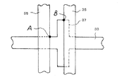
- Patent Document 1 With respect to such a short-circuit problem due to the etching residue 36, in Patent Document 1, as shown in FIG. 12, between the plurality of second wirings 35 passing over the stepped portion of the first wiring 33. Thus, the protrusion 37 is provided in the first wiring shape. Thereby, the length of the step portion of the first wiring 33 is increased, and the possibility that the etching residue of the second wiring 35 is connected and short-circuited can be reduced, and an effective semiconductor device can be provided. It is described.
- JP 7-122632 A (published on May 12, 1995)
- An object of the present invention is to provide a semiconductor device that can reliably prevent a short circuit due to an etching residue generated below a stepped portion and improve the manufacturing yield of a semiconductor device having a multilayer wiring structure, particularly a liquid crystal display device, and a manufacturing method thereof It is to be.
- a semiconductor device and a manufacturing method thereof according to the present invention include a lower layer wiring formed on a substrate, an interlayer insulating film covering the lower layer wiring, and a first upper layer wiring disposed on the interlayer insulating film so as to intersect the lower layer wiring. And a second upper layer wiring, and a step adjustment convex portion is provided between the first upper layer wiring and the second upper layer wiring and close to the side of the lower layer wiring. It is said.
- intermediate steps are arranged in parallel on the interlayer insulating layer, and step-shaped individually divided small steps are formed. Due to the presence of the intermediate step, etching residue hardly occurs in the step portion when the upper layer wiring is formed across the gate wiring. Therefore, it is possible to prevent the first upper layer wiring and the second upper layer wiring from being short-circuited at the step portion.
- the step adjustment convex portion can be formed using an interlayer film such as an insulator, a semiconductor film, or a conductive pair film provided between the substrate and the lower layer wiring.
- an interlayer film such as an insulator, a semiconductor film, or a conductive pair film provided between the substrate and the lower layer wiring.
- the present invention it is possible to reliably prevent a short circuit due to an etching residue generated at the lower portion of the step portion, and to improve the manufacturing yield of a semiconductor device having a multilayer wiring structure.
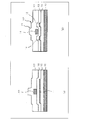
- FIG. 6 is a cross-sectional view (part 1) illustrating the method for manufacturing the first semiconductor device.
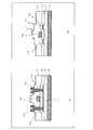
- FIG. 6 is a cross-sectional view (part 2) illustrating the method for manufacturing the first semiconductor device.
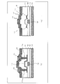
- FIG. 11 is a cross-sectional view (part 3) illustrating the method for manufacturing the first semiconductor device.
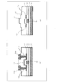
- It is a top view which shows the 2nd semiconductor device of this invention. It is sectional drawing (the 1) which shows the manufacturing method of a 2nd semiconductor device. It is sectional drawing (the 2) which shows the manufacturing method of a 2nd semiconductor device. It is sectional drawing (the 3) which shows the manufacturing method of a 2nd semiconductor device.
- FIG. 11 is a cross-sectional view taken along a line AA in FIG. 10. It is a top view which shows the other conventional multilayer wiring structure.
- FIG. 1 is a top view showing a part of the drive circuit of the liquid crystal display device 1 according to the first embodiment.
- a driving circuit is configured by the top gate type TFT 3.
- an active layer 11 of a TFT 3 is selectively formed on a transparent substrate 10, and this active layer 11 is covered with an interlayer insulating film (not shown). ing.
- the gate electrode 13 of the TFT 3 and the gate wiring 14 which is a lower layer wiring are formed on the interlayer insulating film.
- the gate electrode 13 is disposed so as to pass over the active layer 11, and a top gate type TFT 3 is formed.
- the gate electrode 13 is connected to the gate wiring 14. Since the gate wiring 14 is a wiring arranged in the lower layer in the liquid crystal display device 1, it is also referred to as a lower wiring in the present invention.
- An interlayer insulating film 17 is formed on the gate electrode 13 and the gate wiring 14, and upper wirings 18a to 18f are formed on the interlayer insulating film 17.
- the upper layer wirings 18a to 18d are connected to the source / drain of the semiconductor layer 11 through a contact hole 17a formed in the interlayer insulating film 17, and the upper layer wiring 18f is connected to the gate wiring 14 through a contact hole 17b. ing.
- the step adjustment convex portion 12 is provided on both sides of the gate wiring 14 so as not to overlap the gate wiring 14.
- the step adjustment convex portion 12 can be formed using an interlayer film such as an insulating film, a semiconductor film, or a conductor film provided between the substrate and the lower layer wiring. Thereby, in the manufacturing process of the top gate type TFT, the step adjustment convex part 12 can be formed without increasing the number of processes.
- FIGS. 2 to 4 are cross sections showing a method of manufacturing the liquid crystal display device 1 according to the first embodiment in the order of steps.
- (a) is a cross section taken along the line AA (TFT portion) in FIG.
- (B) is a cross section taken along line BB (step adjustment convex portion) in FIG.
- a method for manufacturing the liquid crystal display device 1 will be described with reference to FIGS. 1 and 2 to 4.
- a silicon oxide film having a thickness of 100 to 300 nm is formed as a first interlayer insulating film 15 on a transparent substrate 10 such as glass.
- a polycrystalline silicon film is formed on the first interlayer insulating film 15 to a thickness of 30 to 150 nm.
- This polycrystalline silicon film is etched into an island shape by dry etching or the like to form the active layer 11 (FIG. 2a) of the TFT 3 and the step adjustment protrusion 12 (FIG. 2b) in a predetermined region.
- the position where the step adjustment convex portion 12 is provided is where the upper wiring 18 formed above is easily short-circuited due to the etching residue.
- the step adjustment convex portion 12 is provided only between the upper layer wirings 18 that are desired to prevent a short circuit. This is because the parasitic capacitance generated in the circuit increases and causes a signal delay.
- the height of the step adjustment protrusion 12 is preferably lower than the height of the gate wiring 14 so as to be formed as an intermediate step lower than the height of the gate wiring 14. Desirably, the gate wiring 14 is formed with a height of about half of the height.
- the height of the step adjustment protrusion 12 can be adjusted by adjusting the film thickness of the active layer 11 and the etching depth of the surface layer of the first interlayer insulating film 15.
- a second interlayer insulating film 16 such as a silicon oxide film covering the active layer 11 and the step adjustment protrusion 12 is formed to a thickness of 50 to 200 nm.
- a first conductor film such as Cr, Mo, Al or the like is formed on the second interlayer insulating film 16 to 200 to 600 nm, and the first conductor film is patterned to form the gate electrode 13 and A gate wiring 14 is formed.
- the gate electrode 13 is disposed so as to pass above the active layer 11 of the TFT 3 as shown in FIG. Using this gate electrode 13 as a mask, an impurity such as phosphorus or boron is introduced into the active layer 11 to form a source / drain in the active layer 11.
- the gate wiring 14 is connected to the gate electrode 13, and as shown in FIG. 2B, a part of the gate wiring 14 is disposed so as to pass between the pair of step adjustment protrusions 12 formed earlier.
- a third interlayer insulating film 17 such as a silicon oxide film covering the gate electrode 13 and the gate wiring 14 is formed to 300 to 600 nm.
- a sputtering method or a P-CVD method can be used as a method for forming the third interlayer insulating film 17.
- Steps reflecting the heights of the gate electrode 13, the gate wiring 14, and the step adjustment protrusion 12 are formed on the third interlayer insulating film 17.
- a large step that reflects the height of the gate wiring 14 as it is is formed on the gate wiring 14 in which the step adjustment convex portion 12 is not provided side by side.
- FIG. 2B the step h2 is formed by the step adjustment convex portion 12 next to the step h1 by the gate wiring 14, and a stepped step formed in two steps is formed.
- step adjustment protrusions 12 on both sides of the gate wiring 14 so as not to overlap the gate wiring 14 so as not to overlap the gate wiring 14. It is formed. For this reason, each step of the staircase shape is reduced, and it is possible to make it difficult for etching residue to occur in the stepped portion.
- step adjustment convex portion 12 at about half the height of the gate wiring 14, the step difference between h1 and h2 is equalized, and one step becomes larger and etching residue tends to occur. Can be prevented.
- contact holes 17 a from which the source / drain regions 11 a of the active layer 11 are exposed and contact holes 17 b from which part of the gate wiring 14 is exposed are formed in the third interlayer insulating film 17. Form.
- a second conductor film 18 made of Al or the like is formed to 400 to 600 nm on the entire surface of the substrate.
- a method for forming the second conductor film 18 a sputtering method or a P-CVD method can be used.
- the second conductor film 18 is electrically connected to the source / drain of the active layer 11 of the TFT through the contact hole 17a, and is connected to the gate wiring 14 through the contact hole 17b.
- the second conductor film 18 is formed following the step shape on the interlayer insulating film 17, but the step on the interlayer insulating film 17 is a staircase where the step adjusting protrusion 12 is provided, as described above. Therefore, the conductive film 18 is not formed thick at the step, and it is possible to prevent the etching residue from being easily generated.
- a resist film is applied on the second conductor film 18 so that the resist film 20 remains only on the portions that become the upper wirings 18a to 18f. Perform development processing.
- a small step-like step reflecting the step on the interlayer insulating film 17 is formed on the conductor film 18 at the portion where the step adjustment convex portion 12 is provided. Therefore, the residue of the resist film 20 is prevented from being generated at each step.
- the second conductor film 18 is patterned by wet etching or dry etching to form upper wirings 18a to 18f as shown in FIG.
- a step adjustment protrusion is provided between the first upper layer wiring 18b and the second upper layer wiring 18c arranged so as to intersect with the gate wiring 14.
- the part 12 is arranged.
- the step formed on the interlayer insulating film 17 is reduced in a stepped manner at the portion where the step adjustment convex portion 12 is provided, and the conductor film 18 is formed thickly on the step portion, or the resist film 20 Since the generation of a residue is prevented, as shown in FIG. 4B, etching residue of the conductor film 18 can be prevented at the step portion. For this reason, the first upper-layer wiring 18b and the second upper-layer wiring 18c, which are arranged so as to intersect with the gate wiring 14 which is the lower-layer wiring, are not short-circuited by the etching residue, thereby improving the manufacturing yield of the semiconductor device. be able to.
- the step adjustment convex portion 12 has been described using the active layer 11 provided between the substrate and the lower layer wiring.
- an insulating film or a conductor film provided between the substrate and the lower layer wiring has been described.
- Other interlayer films can also be used, and they can be formed without increasing the number of processes of the semiconductor device, and are particularly suitable for a multilayer wiring structure formed together with a top gate type TFT.
- FIG. 5 is a top view showing a part of the drive circuit of the liquid crystal display device 2 according to the second embodiment.
- the difference between the second embodiment and the first embodiment is that the bottom gate type TFT 4 is formed in the drive circuit, and the other configuration is the same as that of the first embodiment.
- the drive circuit of the liquid crystal display device 2 is formed with a bottom gate TFT 4 in which a gate electrode 13 is disposed below the active layer 11.
- the other configuration is the same as that of the first embodiment, and the step adjustment protrusions 12 are on both sides of the gate wiring 14 and intersect with the gate wiring 14 and are formed above the first upper layer wiring 18b and the second upper wiring 18b. It is provided between the upper layer wiring 18c.
- the step generated in the interlayer insulating film 17 on the gate wiring 14 is divided into two stages. Becomes smaller. For this reason, when the upper layer wiring 18 is formed on the interlayer insulating film 17, an etching residue hardly occurs in the step portion, and a short circuit between the first upper layer wiring 18b and the second upper layer wiring 18c crossing the step portion is prevented. Can be prevented.
- Example 2 the method of forming the step adjustment convex portion 12 is different, and an interlayer film such as an insulating film, a semiconductor film, or a conductor film provided between the gate wiring 14 as the lower layer wiring and the upper layer wiring 18 is formed. It is formed using. As a result, the step adjustment convex portion 12 can be formed at the same time in the manufacturing process of the bottom gate type TFT 4, thereby preventing an increase in manufacturing cost.
- an interlayer film such as an insulating film, a semiconductor film, or a conductor film provided between the gate wiring 14 as the lower layer wiring and the upper layer wiring 18 is formed. It is formed using.
- the step adjustment convex portion 12 can be formed at the same time in the manufacturing process of the bottom gate type TFT 4, thereby preventing an increase in manufacturing cost.
- FIGS. 6 to 8 are cross sections showing a manufacturing method of the liquid crystal display device according to the second embodiment in the order of steps.
- (a) is a cross section taken along the line AA (TFT portion) in FIG.
- FIG. 5B is a cross section taken along the line BB (step adjustment convex portion) in FIG.
- a method for manufacturing the liquid crystal display device 2 according to the second embodiment will be described with reference to FIGS. 5 and 6 to 8.
- a silicon oxide film having a thickness of 100 to 300 nm is formed as a first interlayer insulating film 15 on a transparent substrate 10 such as glass.
- a first conductor film made of Cr, Mo, Al or the like is formed to 200 to 600 nm, and the first conductor film is patterned to form the gate electrode 13 and the gate wiring 14 as the lower layer wiring.
- a second interlayer insulating film 16 such as a silicon oxide film covering the gate electrode 13 and the gate wiring 14 is formed to a thickness of 50 to 200 nm.
- a semiconductor film such as polycrystalline silicon is formed on the second interlayer insulating film 16 to a thickness of 30 to 150 nm.
- This semiconductor film is etched into an island shape by dry etching or the like, and the active layer 11 of the TFT 4 disposed across the gate electrode 13 shown in FIG. 6A and the step adjustment protrusion shown in FIG. Part 12 is formed.
- the position where the step adjustment convex portion 12 is provided is a portion where the upper wiring 18 formed above is easily short-circuited due to the etching residue. Specifically, as shown in FIG. 5, the first upper-layer wiring 18 b and the second upper-layer wiring 18 b that are formed on both sides of the gate wiring 14 formed earlier and intersect with the gate wiring 14 later. This is a place between the upper layer wiring 18c.
- the step adjustment convex portion 12 is provided only between the upper layer wirings 18 that are desired to prevent a short circuit. This is because the parasitic capacitance generated in the circuit increases and causes a signal delay.
- the step adjustment convex portion 12 is preferably lower than the height of the gate wiring 14 so as to be formed as an intermediate step lower than the height of the gate wiring 14.
- the gate wiring 14 is formed with a height of about half of the height.
- the height of the step adjustment protrusion 12 can be adjusted by adjusting the film thickness of the active layer 11 and the etching depth of the surface layer of the interlayer insulating film 16.
- a third interlayer insulating film 17 such as a silicon oxide film covering the active layer 11 and the step adjustment convex portion 12 is formed to 300 to 600 nm.
- a sputtering method or a P-CVD method can be used as a method for forming the third interlayer insulating film 17.
- Steps reflecting the heights of the gate electrode 13, the gate wiring 14, and the step adjustment protrusion 12 are formed on the third interlayer insulating film 17.
- a large step that reflects the height of the gate wiring 14 as it is is formed on the gate wiring 14 in which the step adjustment convex portion 12 is not provided side by side.
- FIG. 6B the step h2 is formed by the step adjustment convex portion 12 next to the step h1 by the gate wiring 14, and a stepped step formed in two steps is formed.
- step adjustment convex portion 12 As described above, by providing the step adjustment convex portion 12 on both sides of the gate wiring 14 so as not to overlap with the gate wiring 14, a two-step stepped step is formed on the interlayer insulating film 17. In addition, since the respective steps are reduced, it is possible to make it difficult for etching residue to occur in the stepped portion. In addition, by forming the step adjustment convex portion 12 at about half the height of the gate wiring 14, the step difference between h1 and h2 is equalized, and one step becomes larger and etching residue tends to occur. Can be prevented.
- a contact hole 17a that exposes part of the source / drain of the active layer 11 and a contact hole 17b that exposes part of the gate wiring 14 are formed in the third interlayer insulating film 17.
- a second conductor film 18 made of Al or the like is formed to 400 to 600 nm on the entire surface of the substrate.
- a method for forming the second conductor film 18 a sputtering method or a P-CVD method can be used.
- the second conductor film 18 is electrically connected to the source / drain of the active layer 11a of the TFT through the contact hole 17a, and is connected to the gate wiring 14 through the contact hole 17b.
- the second conductor film 18 is formed following the step shape on the interlayer insulating film 17. However, at the portion where the step adjustment convex portion 12 is provided, the step is formed in a small step shape as described above. Therefore, it is possible to reduce the thickness of the conductive film 18 at the stepped portion, and to prevent the etching residue from being easily generated.
- a resist film 20 is applied on the second conductor film 18, and exposure is performed so that the resist film 20 remains only on portions that become the upper wirings 18a to 18f. -Perform development processing.
- FIG. 7B a step-like small step is formed on the conductor film 18 at the portion where the step adjustment convex portion 12 is provided. Therefore, the resist film 20 is formed at each step. Is prevented from occurring.
- the second conductor film 18 is patterned by wet etching or dry etching to form upper layer wirings 18a to 18f.
- the step adjustment convex portion 12 is disposed between the first upper-layer wiring 18b and the second upper-layer wiring 18c disposed so as to intersect with the gate wiring.
- the steps formed on the interlayer insulating film 17 are stepped and individually reduced at the portions where the step adjustment protrusions 12 are provided, and the conductor film 18 is formed on the step portions. Since it is prevented that the resist film 20 is formed thickly and the resist film 20 is not formed, etching residue of the conductor film 18 can be prevented. Therefore, the manufacturing yield of the semiconductor device is improved without causing a short circuit between the first upper-layer wiring 18b and the second upper-layer wiring 18c arranged crossing the gate wiring 14, which is the lower-layer wiring, due to the etching residue. be able to.
- the step adjustment convex portion 12 has been described using the example of the semiconductor film provided between the lower layer wiring and the upper layer wiring. However, an insulating film, a conductor film, or the like provided between the substrate and the lower layer wiring is described. It is also possible to form using other interlayer films. Therefore, the semiconductor device can be formed without increasing the number of processes, and is particularly suitable for a multilayer wiring structure formed together with a bottom gate type TFT.
- FIG. 9 is a cross-sectional view showing a modification of the step adjustment convex portion 12 according to the third embodiment.
- the third embodiment has a structure in which the second step adjustment convex portion 19 is overlapped on the inner side (lower layer wiring side) of the step adjustment convex portion 12 of the first embodiment.
- three stepped steps h1 to h3 reflecting the lower layer wiring 14, the second step adjustment convex portion 19, and the first step adjustment convex portion 12 are formed on the interlayer insulating film 17, Since the level difference is further reduced, a short circuit due to the etching residue can be prevented more reliably.
- the second step adjustment convex portion 19 is formed by forming a first step adjustment convex portion 12 using a semiconductor film and subsequently forming a conductor film such as Al.
- the first step adjustment convex portion 12 can be formed by being etched in an island shape overlapping the inner side (lower layer wiring side). For the etching, dry etching or wet etching that can selectively etch the conductor film can be used.
- the heights of the first step adjustment convex portion 12 and the second step adjustment convex portion 19 are about 1/3 of the height of the lower layer wiring 14, respectively.
- the three stepped steps formed on the interlayer insulating film 17 are equalized, and it is possible to prevent any one of the steps from becoming large and easily causing etching residue.
- the modification of the step adjustment convex portion 12 described in the third embodiment can also be implemented in the liquid crystal display device 2 of the second embodiment.
- the first step adjustment protrusion 12 can be formed of a conductor film
- the second step adjustment protrusion 19 can be formed of a semiconductor film.
- the present invention can be used as a liquid crystal display device provided with a drive circuit composed of a thin film transistor, and a method for using the liquid crystal display device.
Landscapes
- Physics & Mathematics (AREA)
- Nonlinear Science (AREA)
- Engineering & Computer Science (AREA)
- Microelectronics & Electronic Packaging (AREA)
- Mathematical Physics (AREA)
- Chemical & Material Sciences (AREA)
- Crystallography & Structural Chemistry (AREA)
- General Physics & Mathematics (AREA)
- Optics & Photonics (AREA)
- Liquid Crystal (AREA)
- Internal Circuitry In Semiconductor Integrated Circuit Devices (AREA)
- Thin Film Transistor (AREA)
Abstract
基板上に形成された下層配線と、下層配線を覆う層間絶縁膜と、層間絶縁膜上に下層配線と交差して配置された第1の上層配線(18b)と第2の上層配線(18c)とを有し、第1の上層配線(18b)と第2の上層配線(18c)との間であり、且つ、下層配線の側部に近接して、段差調整凸部を設けた。
Description
本発明は、半導体装置およびその製造方法に関し、特に薄膜トランジスタにより構成される駆動回路を備えた液晶表示装置に好適な半導体装置およびその製造方法に関するものである。
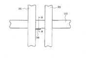
近年、半導体装置の微細化が進むにつれて、多層配線構造を有するようになってきている。多層配線構造は、図10の平面図、及び、図11のA-A部断面図に示すように、基板31上に層間絶縁膜32、34で絶縁された下層配線33が設けられており、この下層配線33の上方に上層配線35が交差して配置されている。このような多層配線構造を用いることにより、レイアウト設計の容易化とチップ面積の縮少化を実現できる反面、上層配線35が下層配線33の段差部をまたいで配線されるため、特に上層配線35が下層配線33の段差部を狭い間隔で配線される際には、上層配線間35の短絡という問題が発生する。
これは、最近の配線形成プロセスで異方性ドライエッチングが用いられ、レジストパターン通りに配線される反面、急峻な段差部が生じ、その上層配線の金属膜厚が大きくなり、エッチング残りが発生し易くなるためである。上層配線間隔が狭くなればこの問題が発生する可能性は大きくなる。
例えば、従来の多層配線構造では、下層配線33の段差部をまたいで上層配線35が配線されると、下層配線33の段差部に沿って上層配線35のエッチング残り36が発生し、このエッチング残り36が上層配線35間でつながることにより短絡が生じる。
このようなエッチング残り36による短絡の問題に対して、特許文献1では、図12に示すように、第1の配線33の段差部の上を通過する、複数本の第2の配線35の間で、第1の配線形状に突起37を設けている。これによって、第1の配線33の段差部の長さが大きくなり、第2の配線35のエッチング残りがつながり短絡する可能性を低減させることができ、有効な半導体装置を提供することができる、と記載されている。
しかしながら、特許文献1の方法では、第2の配線35の短絡する可能性を低減できたとしても、段差部ではエッチング残りが依然として解消されていないため、第2の配線35の短絡を確実に防止することはできなかった。
本発明の目的は、段差部分の下部に発生するエッチング残りによる短絡を確実に防止できて、多層配線構造を有する半導体装置、特に液晶表示装置の製造歩留りを向上できる半導体装置及びその製造方法を提供することである。
本発明に係る半導体装置およびその製造方法は、基板上に形成された下層配線と、下層配線を覆う層間絶縁膜と、層間絶縁膜上に下層配線と交差して配置された第1の上層配線と第2の上層配線とを有し、第1の上層配線と第2の上層配線との間であり、且つ、下層配線の側部に近接して、段差調整凸部を設けたことを特徴としている。
上記の構成を備えることよって、層間絶縁層上には中間段差が並設され、階段状の個々に分断された小さな段差が形成される。上記中間段差が存在することによって、ゲート配線をまたいで上層配線を形成したときに、段差部にエッチング残りが生じ難くなる。したがって、第1の上層配線と第2の上層配線が段差部で短絡することを防止できる。
また、上記段差調整凸部は、基板と下層配線との間に設けられる絶縁体、半導体膜、導電対膜などの層間膜を用いて形成することができる。これにより、工程数を増やさずに段差調整凸部を形成することができる。
本発明によれば、段差部分の下部に発生するエッチング残りによる短絡を確実に防止できて、多層配線構造を有する半導体装置の製造歩留りを向上することができる。
以下、本発明の半導体装置の好ましい実施形態について、図面を参照しながら説明する。
図1は、実施例1である液晶表示装置1の駆動回路の一部を示した上面図である。実施例1では、トップゲート型のTFT3により駆動回路が構成されている。
図1に示すように、液晶表示装置1の駆動回路は、透明基板10上にTFT3の活性層11が選択的に形成されており、この活性層11は層間絶縁膜(不図示)に覆われている。この層間絶縁膜上にはTFT3のゲート電極13と下層配線であるゲート配線14が形成されている。ゲート電極13は、活性層11の上方を通るように配置され、トップゲート型TFT3が形成されている。また、ゲート電極13はゲート配線14に接続されている。このゲート配線14は、液晶表示装置1において下層に配置される配線であるため、本発明では下層配線とも呼称する。
これらのゲート電極13及びゲート配線14上には層間絶縁膜17が形成されており、この層間絶縁膜17上には上層配線18a~18fが形成されている。上層配線18a~18dは、層間絶縁膜17に形成されたコンタクホール17aを介して半導体層11のソース・ドレインに接続されており、上層配線18fはコンタクホール17bを介してゲート配線14に接続されている。
図1の平面視において、本発明では、上層配線18a~18fのうち、下層配線のゲート配線14と交差して配置される第1の上層配線18bと第2の上層配線18cとの間であり、且つ、ゲート配線14の両側部にゲート配線14と重ならないよう近接させて、段差調整凸部12を設けたことを特徴としている。
後で詳しく説明するが、段差調整凸部12をゲート配線14の両側部に設けることにより、層間絶縁膜17上に、ゲート配線14の段差を相対的に小さくする中間段差が並設され、階段状の個々に分断された小さな段差が形成される。このため、ゲート配線14をまたいで上層配線18を形成したときに、段差部にエッチング残りが生じ難くなり、第1の上層配線18bと第2の上層配線18cが段差部で短絡することを防止できる。
この段差調整凸部12は、基板と下層配線との間に設けられる、絶縁膜、半導体膜、導電体膜などの層間膜を用いて形成することができる。これにより、トップゲート型TFTの製造工程において、工程数を増やさずに段差調整凸部12を形成することができる。
図2~図4は、実施例1である液晶表示装置1の製造方法を工程順に示す断面であり、各図において、(a)は図1のA-A線(TFT部)における断面であり、(b)は図1のB-B線(段差調整凸部)における断面である。以下、図1、及び、図2~図4の図面を参照して、液晶表示装置1の製造方法について説明する。
まず、図2に示すように、ガラスなどの透明基板10上に、第1の層間絶縁膜15として、厚さが100~300nmの酸化シリコン膜を形成する。続いて、第1の層間絶縁膜15上に多結晶シリコン膜を30~150nmの厚さに形成する。この多結晶シリコン膜をドライエッチングなどにより島状にエッチングして、所定の領域にTFT3の活性層11(図2a)と、段差調整凸部12(図2b)を形成する。
段差調整凸部12を設ける位置は、上方に形成される上層配線18がエッチング残りにより短絡し易い個所である。具体的には、図1で示したように、後で形成されるゲート配線14の両側部であり、ゲート配線14と交差して上方に形成される第1の上層配線18bと第2の上層配線18cとの間となる個所である。
このように短絡を防止したい上層配線18間にのみ段差調整凸部12を設けるのは、段差調整凸部12をゲート配線14の全長にわたって配置すると、段差調整凸部12とゲート配線14との間に生じる寄生容量が大きくなって信号の遅延を招くためである。
段差調整凸部12の高さは、ゲート配線14の高さよりも低い中間段差として形成されるように、ゲート配線14の高さより低くするのがよい。望ましくは、ゲート配線14の高さの約半分程度の高さで形成するのがよい。この段差調整凸部12の高さは、活性層11の膜厚と、第1の層間絶縁膜15の表層のエッチング深さを合せて調整することができる。
次に、活性層11と段差調整凸部12とを覆う酸化シリコン膜などの第2の層間絶縁膜16を50~200nm形成する。続いて、第2の層間絶縁膜16上に、Cr、Mo、Alなどの第1の導電体膜を、200~600nm形成し、この第1の導電体膜をパターニングして、ゲート電極13とゲート配線14を形成する。
ゲート電極13は、図2(a)のように、TFT3の活性層11の上方を通るように配置される。このゲート電極13をマスクとして活性層11に燐や硼素などの不純物を導入し、活性層11にソース・ドレインを形成する。
また、ゲート配線14はゲート電極13を接続し、図2(b)のように、ゲート配線14の一部が先に形成した一対の段差調整凸部12の間を通るように配置される。
次に、ゲート電極13及びゲート配線14を覆う酸化シリコン膜などの第3の層間絶縁膜17を300~600nm形成する。この第3の層間絶縁膜17の形成方法としては、スパッタ法やP-CVD法を用いることができる。
第3の層間絶縁膜17上には、ゲート電極13、ゲート配線14、段差調整凸部12のそれぞれの高さを反映した段差が形成される。段差調整凸部12が並設されていないゲート配線14上では、ゲート配線14の高さをそのまま反映した大きな段差が形成されるが、段差調整凸部12に隣接したゲート配線14上では、図2(b)のように、ゲート配線14によるh1の段差の隣に段差調整凸部12によるh2の段差が形成され、2段階に連なった階段状の段差が形成される。
このように、ゲート配線14の両側部に、ゲート配線14と重ならないよう近接させて、段差調整凸部12を設けることにより、層間絶縁膜17上には2段になった階段状の段差が形成される。このため、階段状のそれぞれの段差が小さくなり、段差部にエッチング残りを生じ難くすることができる。また、段差調整凸部12をゲート配線14の約半分程度の高さで形成することにより、h1とh2の段差が均等化されて、一方の段差が大きくなってエッチング残りが生じ易くなることを防止できる。
次に、図1に示したように、第3の層間絶縁膜17に、活性層11のソース・ドレイン領域11aが露出するコンタクトホール17aや、ゲート配線14の一部が露出するコンタクトホール17bを形成する。
次に、図3(a)、(b)に示すように、基板上の全面にAlなどの第2の導電体膜18を400~600nm形成する。この第2の導電体膜18の形成方法としては、スパッタ法やP-CVD法を用いることができる。第2の導電体膜18は、コンタクトホール17aを介してTFTの活性層11のソース・ドレインに電気的に接続され、コンタクトホール17bを介してゲート配線14に接続される。
第2の導電体膜18は、層間絶縁膜17上の段差形状に倣って形成されるが、段差調整凸部12を設けた個所では、上記したように、層間絶縁膜17上の段差が階段状に小さく形成されているため、導電体膜18が段差に厚く形成されることがなくなり、エッチング残りが生じ易くなることを防止できる。
次に、図3(a)に示すように、第2の導電体膜18上にレジスト膜を塗布して、上層配線18a~18fとなる部分の上にのみレジスト膜20が残るように露光・現像処理を行う。このとき、段差調整凸部12を設けた個所では、図3(b)に示すように、導電体膜18上には層間絶縁膜17上の段差を反映した階段状の小さな段差が形成されるため、それぞれの段差にレジスト膜20の残渣が生じることが防止される。
次に、レジスト膜20をマスクとし、第2の導電体膜18を湿式エッチングやドライエッチングによりパターニングして、図4(a)に示すように、上層配線18a~18fを形成する。これらの上層配線18a~18fのうち、ゲート配線14と交差して配置される第1の上層配線18bと第2の上層配線18cとの間には、図1に示したように、段差調整凸部12が配置されることになる。
上記のように、段差調整凸部12を設けた個所では、層間絶縁膜17上に形成される段差が階段状に小さくなり、段差部に導電体膜18が厚く形成されたり、レジスト膜20の残渣が生じたりすることが防止されるので、図4(b)に示すように、段差部に導電体膜18のエッチング残りを防止できる。このため、下層配線であるゲート配線14と交差して配置される、第1の上層配線18bと第2の上層配線18cとがエッチング残りで短絡することがなくなり、半導体装置の製造歩留りを向上することができる。
この段差調整凸部12は、基板と下層配線との層間に設けられる活性層11を用いて形成した例を説明したが、基板と下層配線との層間に設けられる絶縁膜や導電体膜などの他の層間膜を用いることも可能であり、半導体装置の工程数を増やさずに形成することができ、特に、トップゲート型TFTと一緒に形成される多層配線構造に適している。
図5は、実施例2である液晶表示装置2の駆動回路の一部を示した上面図である。実施例2において実施例1と異なるところは、駆動回路にボトムゲート型TFT4が形成されていることであり、他は実施例1の構成と同じであるため、詳細な説明は省略する。
図5に示すように、液晶表示装置2の駆動回路は、活性層11の下方にゲート電極13が配置されたボトムゲート型TFT4が形成されている。他の構成は実施例1と同じであり、段差調整凸部12が、ゲート配線14の両側部であり、ゲート配線14と交差して上方に形成される第1の上層配線18bと第2の上層配線18cとの間に設けられている。
段差調整凸部12をゲート配線14の両側部に、ゲート配線14と重ならないよう近接させて設けることにより、ゲート配線14上の層間絶縁膜17に生じる段差が2段に分割され、それぞれの段差は小さくなる。このため、層間絶縁膜17上に上層配線18を形成したときに、段差部にエッチング残りが生じ難くなり、段差部を交差する第1の上層配線18bと第2の上層配線18cとの短絡を防止することができる。
実施例2では、この段差調整凸部12の形成方法が異なり、下層配線であるゲート配線14と、上層配線18との層間に設けられる、絶縁膜、半導体膜、導電体膜などの層間膜を用いて形成している。これにより、ボトムゲート型TFT4の製造過程において段差調整凸部12を同時に形成することができ、製造コストが嵩むことを防止している。
図6~図8は、実施例2である液晶表示装置の製造方法を工程順に示す断面であり、各図において、(a)は図5のA-A線(TFT部)における断面であり、(b)は図5のB-B線(段差調整凸部)における断面である。以下に、図5、及び、図6~図8の図面を参照して、実施例2における液晶表示装置2の製造方法について説明する。
まず、図6に示すように、ガラスなどの透明基板10上に、第1の層間絶縁膜15として、厚さが100~300nmの酸化シリコン膜を形成する。続いて、Cr、Mo、Alなどの第1の導電体膜を、200~600nm形成し、この第1の導電体膜をパターニングしてゲート電極13と下層配線であるゲート配線14を形成する。次に、ゲート電極13とゲート配線14を覆う酸化シリコン膜などの第2の層間絶縁膜16を50~200nm形成する。
次に、第2の層間絶縁膜16上に多結晶シリコンなどの半導体膜を30~150nmの厚さに形成する。この半導体膜をドライエッチングなどにより島状にエッチングして、図6(a)に示す、ゲート電極13を跨いで配置されるTFT4の活性層11と、図6(b)に示す、段差調整凸部12が形成される。
段差調整凸部12を設ける位置は、上方に形成される上層配線18間がエッチング残りにより短絡し易い個所である。具体的には、図5で示したように、先に形成されたゲート配線14の両側部であり、後にゲート配線14と交差して上方に形成される第1の上層配線18bと第2の上層配線18cとの間となる個所である。
このように短絡を防止したい上層配線18間にのみ段差調整凸部12を設けるのは、段差調整凸部12をゲート配線14の全長にわたって配置すると、段差調整凸部12とゲート配線14との間に生じる寄生容量が大きくなって信号の遅延を招くためである。
また、段差調整凸部12は、ゲート配線14の高さよりも低い中間段差として形成されるように、ゲート配線14の高さより低くするのがよい。望ましくは、ゲート配線14の高さの約半分程度の高さで形成するのがよい。この段差調整凸部12の高さは、活性層11の膜厚と、層間絶縁膜16の表層のエッチング深さを合せて調整することができる。
次に、活性層11と段差調整凸部12を覆う酸化シリコン膜などの第3の層間絶縁膜17を300~600nm形成する。この第3の層間絶縁膜17の形成方法としては、スパッタ法やP-CVD法を用いることができる。
第3の層間絶縁膜17上には、ゲート電極13、ゲート配線14、段差調整凸部12のそれぞれの高さを反映した段差が形成される。段差調整凸部12が並設されていないゲート配線14上では、ゲート配線14の高さをそのまま反映した大きな段差が形成されるが、段差調整凸部12に隣接したゲート配線14上では、図6(b)のように、ゲート配線14によるh1の段差の隣に段差調整凸部12によるh2の段差が形成され、2段階に連なった階段状の段差が形成される。
このように、ゲート配線14の両側部にゲート配線14と重ならないよう近接させて、段差調整凸部12を設けることにより、層間絶縁膜17上には2段になった階段状の段差が形成され、それぞれの段差が小さくなるため、段差部にエッチング残りを生じ難くすることができる。また、段差調整凸部12をゲート配線14の約半分程度の高さで形成することにより、h1とh2の段差が均等化されて、一方の段差が大きくなってエッチング残りが生じ易くなることを防止できる。
次に、図5に示したように、第3の層間絶縁膜17に、活性層11のソース・ドレインの一部を露出させるコンタクトホール17aや、ゲート配線14の一部を露出させるコンタクトホール17bを形成する。
次に、図7(a)、(b)に示すように、基板上の全面にAlなどの第2の導電体膜18を400~600nm形成する。この第2の導電体膜18の形成方法としては、スパッタ法やP-CVD法を用いることができる。第2の導電体膜18は、コンタクトホール17aを介してTFTの活性層11aのソース・ドレインに電気的に接続され、コンタクトホール17bを介してゲート配線14に接続される。
第2の導電体膜18は、層間絶縁膜17上の段差形状に倣って形成されるが、段差調整凸部12を設けた個所では、上記したように、段差が階段状に小さく形成されるため、導電体膜18が段差部で厚くなることが緩和され、エッチング残りが生じ易くなることを防止できる。
次に、図7(a)に示すように、第2の導電体膜18上にレジスト膜20を塗布して、上層配線18a~18fとなる部分の上にのみレジスト膜20が残るように露光・現像処理を行う。このとき、段差調整凸部12を設けた個所では、図7(b)に示すように、導電体膜18上には階段状の小さな段差が形成されているため、それぞれの段差にレジスト膜20の残渣が生じることが防止される。
次に、図8(a)に示すように、レジスト膜20をマスクとし、第2の導電体膜18を湿式エッチングやドライエッチングによりパターニングして、上層配線18a~18fを形成する。これらの上層配線18a~18fのうち、ゲート配線14と交差して配置される第1の上層配線18bと第2の上層配線18cとの間には、段差調整凸部12が配置されている。
段差調整凸部12を設けた個所では、図8(b)に示すように、層間絶縁膜17上に形成される段差が階段状となって個々に小さくなり、段差部に導電体膜18が厚く形成されたり、レジスト膜20の残渣が生じたりすることが防止されるので、導電体膜18のエッチング残りを防止することができる。このため、下層配線であるゲート配線14と交差して配置される第1の上層配線18bと第2の上層配線18cとの間がエッチング残りで短絡することなく、半導体装置の製造歩留りを向上することができる。
この段差調整凸部12は、下層配線と上層配線との層間に設けられる半導体膜を用いて形成した例を説明したが、基板と下層配線との層間に設けられる絶縁膜や導電体膜などの他の層間膜を用いて形成することも可能である。このため、半導体装置の工程数を増やさずに形成することができ、特に、ボトムゲート型TFTと一緒に形成される多層配線構造に適している。
図9は、実施例3である段差調整凸部12の変形例を示した断面図である。実施例3は、実施例1の段差調整凸部12の内側(下層配線側)に第2の段差調整凸部19を重ねた構造となっている。上記構造により、下層配線14、第2の段差調整凸部19、第1の段差調整凸部12をそれぞれ反映した3段階の階段状の段差h1~h3が層間絶縁膜17上に形成され、各段差がさらに小さく形成されるので、エッチング残りによる短絡をより確実に防止することができる。
第2の段差調整凸部19は、例えば実施例1で説明したように、半導体膜を用いて第1の段差調整凸部12を形成したあと、続いて、Alなど導電体膜を成膜し、第1の段差調整凸部12の内側(下層配線側)に重ねて島状にエッチングして形成することができる。エッチングは導電体膜を選択的にエッチングできるドライエッチングや湿式エッチングを用いることができる。
第1の段差調整凸部12と、第2の段差調整凸部19の高さは、それぞれ、下層配線14の高さの1/3程度にするのが望ましい。これにより、層間絶縁膜17上に形成される3段階の階段状の段差が均等化されて、いずれか一つの段差が大きくなってエッチング残りが生じ易くなることを防止できる。
実施例3で説明した段差調整凸部12の変形例は、実施例2の液晶表示装置2でも実施することが可能である。また、第1の段差調整凸部12を導電体膜で形成し、第2の段差調整凸部19を半導体膜で形成することもできる。
本発明は、特に薄膜トランジスタにより構成される駆動回路を備えた液晶表示装置およびその利用方法として利用できる。
1、2 液晶表示装置
3 トップゲート型TFT
4 ボトムゲート型TFT
10 基板
11 半導体膜
12 段差調整凸部
13 ゲート電極
14 ゲート配線
15 第1の層間絶縁膜
16 第2の層間絶縁膜
17 第3の層間絶縁膜
18 上層配線
19 第2の段差調整凸部
20 レジスト膜
33 第1の配線
35 第2の配線
36 エッチング残り
37 突起
3 トップゲート型TFT
4 ボトムゲート型TFT
10 基板
11 半導体膜
12 段差調整凸部
13 ゲート電極
14 ゲート配線
15 第1の層間絶縁膜
16 第2の層間絶縁膜
17 第3の層間絶縁膜
18 上層配線
19 第2の段差調整凸部
20 レジスト膜
33 第1の配線
35 第2の配線
36 エッチング残り
37 突起
Claims (10)
- 基板上に形成された下層配線と、前記下層配線を覆う層間絶縁膜と、前記層間絶縁膜上に前記下層配線と交差して配置された第1の上層配線と第2の上層配線とを有し、
前記第1の上層配線と前記第2の上層配線との間であり、且つ、前記下層配線の側部に近接して、段差調整凸部を設けたことを特徴とする半導体装置。 - 前記段差調整凸部の高さは、前記下層配線の高さよりも低いことを特徴とする請求項1に記載の半導体装置。
- 前記段差調整凸部の高さは、前記下層配線の約半分の高さであることを特徴とする請求項2に記載の半導体装置。
- 前記段差調整凸部は、第1の段差調整凸部の前記下層配線側に第2の段差調整凸部を重ねて設けたことを特徴とする請求項1に記載の半導体装置。
- 前記第1の段差調整凸部および前記第2の段差調整凸部のそれぞれの高さは、前記下層配線の約1/3の高さであることを特徴とする請求項4に記載の半導体装置。
- 前記段差調整凸部は、前記基板と前記下層配線との間に備える、絶縁膜、半導体膜、導電体膜のうち少なくともいずれか一つを島状に形成して設けたことを特徴とする請求項1に記載の半導体装置。
- 前記段差調整凸部は、前記下層配線と前記第1及び第2の上層配線との間に備える、絶縁膜、半導体膜、導電体膜のうち少なくともいずれか一つを島状に形成して設けたことを特徴とする請求項1に記載の半導体装置。
- 基板上に第1の層間絶縁膜を形成する工程と、
前記第1の層間絶縁膜上に半導体膜を形成し、この半導体膜を島状にパターニングして段差調整凸部を形成する工程と、
前記段差調整凸部を覆う第2の層間絶縁膜を形成する工程と、
前記第2の層間絶縁膜上に第1の導電体膜を形成し、この第1の導電体膜をパターニングして前記段差調整凸部の側部に近接して配置される下層配線を形成する工程と、
前記下層配線を覆う第3の層間絶縁膜を形成する工程と、
前記第3の層間絶縁膜上に第2の導電体膜を形成する工程と、
前記第2の導電体膜をパターニングして、前記下層配線と交差し且つ前記段差調整凸部を挟んで配置される第1の上層配線と第2の上層配線とを形成する工程とを有することを特徴とする半導体装置の製造方法。 - 基板上に第1の層間絶縁膜を形成する工程と、
前記第1の層間絶縁膜上に第1の導電体膜を形成し、この第1の導電体膜をパターニングして下層配線を形成する工程と、
前記下層配線を覆う第2の層間絶縁膜を形成する工程と、
前記第2の層間絶縁膜上に半導体膜を形成し、この半導体膜を島状にパターニングして、前記下層配線の側部に近接して配置される段差調整凸部を形成する工程と、
前記段差調整凸部を覆う第3の層間絶縁膜を形成する工程と、
前記第3の層間絶縁膜上に第2の導電体膜を形成する工程と、
前記第2の導電体膜をパターニングして、前記下層配線と交差し且つ前記段差調整凸部を挟んで配置される第1の上層配線と第2の上層配線とを形成する工程とを有することを特徴とする半導体装置の製造方法。 - 前記半導体膜を島状にパターニングして、前記段差調整凸部と、TFTの活性層を同時に形成することを特徴とする請求項8または9のいずれかに記載の半導体装置の製造方法。
Priority Applications (1)
| Application Number | Priority Date | Filing Date | Title |
|---|---|---|---|
| US13/704,396 US9064867B2 (en) | 2010-06-23 | 2011-04-20 | Semiconductor device and method for manufacturing same |
Applications Claiming Priority (2)
| Application Number | Priority Date | Filing Date | Title |
|---|---|---|---|
| JP2010-142233 | 2010-06-23 | ||
| JP2010142233A JP2013179102A (ja) | 2010-06-23 | 2010-06-23 | 半導体装置およびその製造方法 |
Publications (1)
| Publication Number | Publication Date |
|---|---|
| WO2011162018A1 true WO2011162018A1 (ja) | 2011-12-29 |
Family
ID=45371221
Family Applications (1)
| Application Number | Title | Priority Date | Filing Date |
|---|---|---|---|
| PCT/JP2011/059735 Ceased WO2011162018A1 (ja) | 2010-06-23 | 2011-04-20 | 半導体装置およびその製造方法 |
Country Status (3)
| Country | Link |
|---|---|
| US (1) | US9064867B2 (ja) |
| JP (1) | JP2013179102A (ja) |
| WO (1) | WO2011162018A1 (ja) |
Citations (1)
| Publication number | Priority date | Publication date | Assignee | Title |
|---|---|---|---|---|
| JPS54134583A (en) * | 1978-04-11 | 1979-10-19 | Toshiba Corp | Forming method of multilayer wiring layer |
Family Cites Families (1)
| Publication number | Priority date | Publication date | Assignee | Title |
|---|---|---|---|---|
| JP2797929B2 (ja) | 1993-10-22 | 1998-09-17 | 日本電気株式会社 | 半導体装置 |
-
2010
- 2010-06-23 JP JP2010142233A patent/JP2013179102A/ja active Pending
-
2011
- 2011-04-20 WO PCT/JP2011/059735 patent/WO2011162018A1/ja not_active Ceased
- 2011-04-20 US US13/704,396 patent/US9064867B2/en not_active Expired - Fee Related
Patent Citations (1)
| Publication number | Priority date | Publication date | Assignee | Title |
|---|---|---|---|---|
| JPS54134583A (en) * | 1978-04-11 | 1979-10-19 | Toshiba Corp | Forming method of multilayer wiring layer |
Also Published As
| Publication number | Publication date |
|---|---|
| JP2013179102A (ja) | 2013-09-09 |
| US9064867B2 (en) | 2015-06-23 |
| US20130087924A1 (en) | 2013-04-11 |
Similar Documents
| Publication | Publication Date | Title |
|---|---|---|
| JP4661913B2 (ja) | 液晶表示装置 | |
| KR102050401B1 (ko) | 디스플레이 장치 및 그 제조방법 | |
| CN114690921A (zh) | 显示面板、显示装置及制作显示面板的方法 | |
| WO2018061851A1 (ja) | アクティブマトリクス基板およびその製造方法 | |
| WO2017051791A1 (ja) | 半導体装置およびその製造方法 | |
| KR20110067765A (ko) | 박막 트랜지스터 표시판 및 그 제조 방법 | |
| JP2019169606A (ja) | アクティブマトリクス基板およびその製造方法 | |
| JP5023465B2 (ja) | 薄膜トランジスタパネル | |
| JP2010097077A (ja) | 表示装置及びその製造方法 | |
| JP5146477B2 (ja) | トランジスタアレイ基板及びその製造方法 | |
| JP2011119469A (ja) | 半導体装置及びその製造方法 | |
| KR960016824B1 (ko) | 반도체장치 및 그의 제조방법 | |
| KR101254479B1 (ko) | 반도체 장치 및 그 제조 방법 | |
| JP5040222B2 (ja) | 表示装置 | |
| TW584908B (en) | Method of manufacturing IPS-LCD by using 4-mask process | |
| CN100452411C (zh) | 半导体结构及其制造方法 | |
| JP4441299B2 (ja) | 表示装置の製造方法 | |
| WO2011162018A1 (ja) | 半導体装置およびその製造方法 | |
| KR20100069935A (ko) | 박막 트랜지스터 어레이 기판 및 이의 제조 방법 | |
| JP3962800B2 (ja) | 液晶表示装置の製造方法 | |
| KR100315914B1 (ko) | 4장의마스크를이용한액정표시장치용박막트랜지스터기판의제조방법및액정표시장치용박막트랜지스터기판 | |
| JP4670263B2 (ja) | 表示装置 | |
| KR100490043B1 (ko) | 평면구동방식의액정표시장치및그제조방법 | |
| KR20090103508A (ko) | 반도체 소자 | |
| KR20000026540A (ko) | 4장의 마스크를 이용한 액정 표시 장치용 박막 트랜지스터 기판의 제조 방법 및 액정 표시 장치용박막 트랜지스터 기판 |
Legal Events
| Date | Code | Title | Description |
|---|---|---|---|
| 121 | Ep: the epo has been informed by wipo that ep was designated in this application |
Ref document number: 11797906 Country of ref document: EP Kind code of ref document: A1 |
|
| WWE | Wipo information: entry into national phase |
Ref document number: 13704396 Country of ref document: US |
|
| NENP | Non-entry into the national phase |
Ref country code: DE |
|
| 122 | Ep: pct application non-entry in european phase |
Ref document number: 11797906 Country of ref document: EP Kind code of ref document: A1 |
|
| NENP | Non-entry into the national phase |
Ref country code: JP |