WO2011155342A1 - 光デバイスおよび光デバイスの製造方法 - Google Patents
光デバイスおよび光デバイスの製造方法 Download PDFInfo
- Publication number
- WO2011155342A1 WO2011155342A1 PCT/JP2011/062118 JP2011062118W WO2011155342A1 WO 2011155342 A1 WO2011155342 A1 WO 2011155342A1 JP 2011062118 W JP2011062118 W JP 2011062118W WO 2011155342 A1 WO2011155342 A1 WO 2011155342A1
- Authority
- WO
- WIPO (PCT)
- Prior art keywords
- side optical
- optical fiber
- face
- incident
- exit
- Prior art date
- Legal status (The legal status is an assumption and is not a legal conclusion. Google has not performed a legal analysis and makes no representation as to the accuracy of the status listed.)
- Ceased
Links
Images



Classifications
-
- G—PHYSICS
- G02—OPTICS
- G02B—OPTICAL ELEMENTS, SYSTEMS OR APPARATUS
- G02B6/00—Light guides; Structural details of arrangements comprising light guides and other optical elements, e.g. couplings
- G02B6/24—Coupling light guides
- G02B6/36—Mechanical coupling means
- G02B6/38—Mechanical coupling means having fibre to fibre mating means
- G02B6/3807—Dismountable connectors, i.e. comprising plugs
- G02B6/381—Dismountable connectors, i.e. comprising plugs of the ferrule type, e.g. fibre ends embedded in ferrules, connecting a pair of fibres
- G02B6/3818—Dismountable connectors, i.e. comprising plugs of the ferrule type, e.g. fibre ends embedded in ferrules, connecting a pair of fibres of a low-reflection-loss type
- G02B6/382—Dismountable connectors, i.e. comprising plugs of the ferrule type, e.g. fibre ends embedded in ferrules, connecting a pair of fibres of a low-reflection-loss type with index-matching medium between light guides
-
- G—PHYSICS
- G02—OPTICS
- G02B—OPTICAL ELEMENTS, SYSTEMS OR APPARATUS
- G02B6/00—Light guides; Structural details of arrangements comprising light guides and other optical elements, e.g. couplings
- G02B6/24—Coupling light guides
- G02B6/36—Mechanical coupling means
- G02B6/38—Mechanical coupling means having fibre to fibre mating means
- G02B6/3807—Dismountable connectors, i.e. comprising plugs
- G02B6/381—Dismountable connectors, i.e. comprising plugs of the ferrule type, e.g. fibre ends embedded in ferrules, connecting a pair of fibres
- G02B6/3818—Dismountable connectors, i.e. comprising plugs of the ferrule type, e.g. fibre ends embedded in ferrules, connecting a pair of fibres of a low-reflection-loss type
- G02B6/3821—Dismountable connectors, i.e. comprising plugs of the ferrule type, e.g. fibre ends embedded in ferrules, connecting a pair of fibres of a low-reflection-loss type with axial spring biasing or loading means
-
- G—PHYSICS
- G02—OPTICS
- G02B—OPTICAL ELEMENTS, SYSTEMS OR APPARATUS
- G02B6/00—Light guides; Structural details of arrangements comprising light guides and other optical elements, e.g. couplings
- G02B6/24—Coupling light guides
- G02B6/36—Mechanical coupling means
- G02B6/40—Mechanical coupling means having fibre bundle mating means
- G02B6/403—Mechanical coupling means having fibre bundle mating means of the ferrule type, connecting a pair of ferrules
Definitions
- the present invention relates to an optical device that optically couples end faces of optical fibers to face each other, and a manufacturing method thereof.
- Patent Document 1 discloses a multi-fiber ferrule for connecting a bundle fiber composed of a plurality of optical fibers and a single optical fiber by a physical contact, and an optical fiber connection structure.
- the input light is visible light, particularly blue visible light
- the optical devices disclosed in Patent Document 2 and Patent Document 3 prevent the above chemical reaction between the optical fibers by forming a protective medium containing fluoride between the facing optical fibers. Yes.
- the protective medium in the optical devices disclosed in Patent Documents 2 and 3 is a film body formed by vapor deposition or ion assist, that is, a so-called solid material, a large pressure load is applied between the optical fibers due to vibration or the like. In such a case, the protective medium itself that protects between the optical fibers may be damaged, and the transmission characteristics may be deteriorated.
- the present invention has been made in view of the above-described problem, and even when a pressure bonding load between optical fibers facing each other is increased due to vibration or the like, the optical device that protects the protective medium itself between the optical fibers is not damaged. And a method of manufacturing the same.
- the optical device of the present invention includes an incident side optical fiber that emits incident light from an emission end surface, and an emission side optical fiber that enters the light emitted from the emission end surface from an incident end surface facing the emission end surface; A protective medium made of a gel-like resin that is interposed between the exit end face and the entrance end face and transmits the light emitted from the exit end face to the entrance end face.
- the protective medium made of gel-like resin is interposed between the exit end face of the entrance side optical fiber and the entrance end face of the exit side optical fiber. Therefore, even when the end surfaces of the incident side optical fiber and the output side optical fiber are rubbed due to vibration or the like, or the pressure load applied between the output end surface of the incident side optical fiber and the incident end surface of the output side optical fiber is increased.
- the protective medium itself is not damaged. Thereby, it is possible to prevent the deterioration of the transmission characteristics of the optical device due to the damage of the protective medium.
- the protective medium may be a gel-like resin made of silicone.
- the protective medium is made of silicone having a small refractive index difference between the incident side optical fiber and the output side optical fiber, it is possible to provide an optical device having good transmission characteristics.
- silicone is excellent in heat resistance, the protective medium hardly changes even when the temperature rises, and since light resistance is also excellent, the refractive index and transmittance of the protective medium hardly change. Therefore, an optical device having good transmission characteristics can be provided.
- the incident side optical fiber may be a multimode optical fiber.
- an optical device that can be easily connected to a light source and can be connected to a high power light source having a large light emitting area.
- a plurality of the incident side optical fibers may be bundled.
- the exit end face of the incident side optical fiber may be polished in a flat shape.
- the light emitted from the exit end face of the incident side optical fiber is transmitted straight to the entrance end face of the exit side optical fiber as compared with the case where it is not polished into a flat shape. Thereby, the light from the incident side optical fiber can be transmitted into the output side optical fiber with low loss.
- the adhesive that bonds and fixes the plurality of incident side optical fibers may have a transmittance at a wavelength of 400 nm of 50% or more and a glass transition temperature of 130 ° C. or more. .
- the adhesive is hardly deteriorated by heat generation due to absorption of leaked light. Therefore, a part of the adhesive peeled off due to the deterioration of the adhesive does not adhere to the protective medium, thereby causing a decrease in transmittance. Thereby, an optical device having good transmission characteristics can be provided.
- the optical device of the present invention includes an incident side optical member that accommodates the incident side optical fiber, an output side optical member that accommodates the output side optical fiber, an output end face of the incident side optical fiber, and the output side light.
- a holding member that holds the incident-side optical member and the emission-side optical member, and the incident-side optical member, the emission-side optical member, and the holding member so as to face the incident end surface of the fiber.
- the holding member that holds the incident side optical member and the emission side optical member is accommodated without being in contact with the holding case. Therefore, since the leaked light is emitted into the air, the leaked light is not easily reabsorbed by the holding member, and the temperature rise of the holding member can be prevented. Furthermore, even when the holding case is deformed by the temperature rise in the holding case, the influence on the holding member can be reduced.
- the manufacturing method in the optical device of the present invention includes an incident side optical fiber that emits incident light from the exit end face, and an exit that enters the light emitted from the exit end face from the entrance end face facing the exit end face.
- a side optical fiber, and a manufacturing method of an optical device comprising: adhering a gel-like resin to one of the exit end face and the entrance end face, and pressing the other to the resin, the exit end face And a protective medium is formed between the incident end face and the incident end face.
- the above manufacturing method it is possible to form a protective medium made of a gel-like resin between the exit end face of the entrance side optical fiber and the entrance end face of the exit side optical fiber. Therefore, even when the end surfaces of the incident side optical fiber and the output side optical fiber are rubbed due to vibration or the like, or the pressure load applied between the output end surface of the incident side optical fiber and the incident end surface of the output side optical fiber is increased.
- the protective medium itself is not damaged. Thereby, it is possible to prevent the deterioration of the transmission characteristics of the optical device due to the damage of the protective medium.
- the resin used for the protective medium is in a gel-like state having no fluidity, it is easy to adhere to the exit end face of the entrance side optical fiber and the entrance end face of the exit side optical fiber, and the working efficiency is good. Furthermore, since the protective medium can be formed simply by pressing the other end face to the adhesive resin, the protective medium can be formed easily in a shorter time than when a film is formed by vapor deposition or ion assist.
- the end faces of the incident-side optical fiber and the outgoing-side optical fiber are rubbed due to vibration or the like, and the pressure load applied between the outgoing end face of the incident-side optical fiber and the incident end face of the outgoing-side optical fiber is increased. Even if it becomes larger, the protective medium itself is not damaged. Thereby, it is possible to prevent the deterioration of the transmission characteristics of the optical device due to the damage of the protective medium.
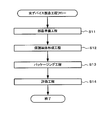
- FIG. 1 It is a flowchart which shows the manufacturing method of the optical device which concerns on embodiment of this invention.
- A It is explanatory drawing which shows before formation of the protection medium based on embodiment of this invention.
- B It is explanatory drawing which shows just before formation of the protection medium based on embodiment of this invention.
- C It is explanatory drawing which shows after formation of the protection medium based on embodiment of this invention.
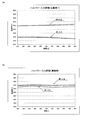
- A It is a figure which shows the high power input evaluation result of the optical device which concerns on the comparative example 1.
- FIG. (B) It is a figure which shows the high power input evaluation result of the optical device which concerns on an Example.
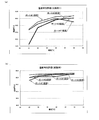
- A It is a figure which shows the temperature characteristic evaluation result of the optical device which concerns on the comparative example 1.
- FIG. (B) It is a figure which shows the temperature characteristic evaluation result of the optical device which concerns on an Example.
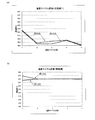
- A) It is a figure which shows the temperature cycle evaluation result of the optical device which concerns on the comparative example 1.
- FIG. (B) It is a figure which shows the temperature cycle evaluation result of the optical device which concerns on an Example.
- A) It is a figure which shows the permeation
- FIG. (B) It is a figure which shows the permeation
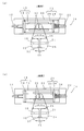
- A) It is explanatory drawing which shows the optical device which concerns on the comparative example 1.
- FIG. (B) It is explanatory drawing which shows the optical device which concerns on the comparative example 2.
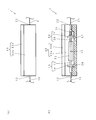
- the optical device 1 As shown in FIGS. 1 and 2, the optical device 1 according to the present embodiment opposes an incident-side optical fiber 10 that emits incident light from an emission end face, and opposes the light emitted from the emission end face to the emission end face.
- An output-side optical fiber 21 that is incident from the incident end face; and a protective medium 50 that is interposed between the exit end face and the incident end face and is made of a gel-like resin 57 that transmits light emitted from the exit end face to the incident end face.
- the optical device 1 includes an incident side optical member 13 that accommodates the incident side optical fiber 10, an emission side optical member 23 that accommodates the emission side optical fiber 21, and an emission end face of the incident side optical fiber 10.
- the holding member 32 that holds the incident side optical member 13 and the emission side optical member 23, and the incident side optical member 13, the emission side optical member 23, and the holding member so as to face the incident end face of the emission side optical fiber 21.
- the holding member 32 is housed in the holding case 33 without being in contact with the holding case 33.
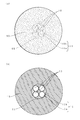
- the incident side optical fiber 10 is a multimode optical fiber. Moreover, as shown in FIG.3 (b), the four incident side optical fibers 10 are bundled. Therefore, it is possible to couple light having the same wavelength, different wavelengths, or different output powers. Further, it can be easily connected to a light source and can be connected to a high power light source having a large light emitting area.
- Each incident-side optical fiber 10 has a core 10a that is a light path at the center, and is configured such that a thin clad 10b covers the peripheral surface thereof.
- the bundled four incident-side optical fibers 10 are bonded and fixed by an adhesive 55 and are accommodated in a through hole formed at the center of the incident-side optical member 13.
- the adhesive 55 is made of a material having a transmittance of 50% or more at a wavelength of 400 nm, a glass transition temperature of 130 ° C. or more, and a Shore hardness of 80 or more, and includes four incident-side optical fibers. 10 are bonded and fixed, and the incident side optical fiber 10 and the inner surface of the incident side optical member 13 are bonded and fixed.
- the reason for using the adhesive 55 having the above-described characteristics is that if the transmittance is less than 50%, the adhesive 55 absorbs leaked light and generates heat, which accelerates the deterioration.
- the glass transition temperature of the adhesive 55 is smaller than 130 ° C., the glass transition temperature may be exceeded due to the temperature rise, and as a result, the transmittance of the optical device 1 may decrease due to the change in physical properties of the adhesive 55. There is. Further, if the Shore hardness of the adhesive 55 is less than 80, it will be excessively shaved during the polishing process in the manufacturing process, resulting in dents, dust adhering to the part, light scattering at the dents, etc. This is because a problem occurs.
- the incident side optical fibers 10 are not limited to four, and a plurality of other incident side optical fibers 10 may be bundled, for example, two, three, or five. Furthermore, the incident side optical fiber 10 may be one.
- the optical fiber used for the incident side optical fiber 10 is not limited to a multimode optical fiber, and a single mode optical fiber can also be used.
- a multimode optical fiber is preferably used as the incident side optical fiber 10 because it can be easily connected to a light source and can be connected to a high power light source having a large light emitting area.
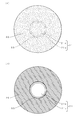
- the emission side optical fiber 21 is composed of a single multimode optical fiber, and has a core 21a that is a light path at the center as in the case of the incidence side optical fiber 10.
- the thin clad 21b covers the peripheral surface.
- the emission side optical fiber 21 is accommodated in a through hole formed at the center of the emission side optical member 23, and an adhesive 55 filled in a gap between the emission side optical fiber 21 and the inner surface of the emission side optical member 23. Is fixed by bonding.
- the core diameter of the exit side optical fiber 21 is set larger than the core diameter of the entrance side optical fiber 10.
- the respective core diameters are set so that the entire area of the core 10 a of the four incident side optical fibers 10 is included in the area of the core 21 a of the emission side optical fiber 21.
- this is because the light emitted from the core of the incident side optical fiber 10 is emitted on the output side during optical coupling between the output end face of the incident side optical fiber 10 and the incident end face of the output side optical fiber 21.
- the signal is transmitted to the core 21a of the optical fiber 21 with low loss.
- the numerical aperture (NA) of the emission side optical fiber 21 is set to be equal to or larger than the numerical aperture (NA) of the incident side optical fiber 10. Thereby, the light emitted from the incident side optical fiber 10 is transmitted into the emission side optical fiber 21 with low loss.
- the incident side optical fiber 10 and the outgoing side optical fiber 21 are arranged so that the outgoing end face of the incoming side optical fiber 10 and the incoming end face of the outgoing side optical fiber 21 face each other as shown in the enlarged portion 35 of FIG. Has been placed.
- a protective medium 50 is interposed between the incident side optical fiber 10 and the output side optical fiber 21.
- the protective medium 50 is made of a gel-like resin 57 that transmits the light emitted from the exit end face of the incident side optical fiber 10 to the entrance end face of the exit side optical fiber 21. As shown in FIGS. 3A and 4A, the protective medium 50 is provided so as to completely cover the exit end face of the incident side optical fiber 10 and the entrance end face of the exit side optical fiber 21. There is no air layer between the incident side optical fiber 10 and the output side optical fiber 21. Therefore, the light input from the incident side optical fiber 10 chemically reacts with a silicon compound in the air to form SiO 2, and the SiO 2 is formed on the outgoing end face of the incident side optical fiber 10 and the incoming end face of the outgoing side optical fiber 21.
- the protective medium 50 is the gel-like resin 57, it has a high viscosity.
- a resin having a penetration degree (JISK2220) of 300 is used for the protective medium 50.
- vibration or the like may occur depending on the usage state of the optical device 1.
- the protective medium 50 is a film body formed by vapor deposition or ion assist on at least one of the exit end face of the entrance side optical fiber 10 and the entrance end face of the exit side optical fiber 21, a so-called solid material is formed on both.
- the protected protective media may collide with each other by vibration or rub against each other, and the protective media themselves may be damaged.
- the protective medium 50 made of the gel-like resin 57 is interposed between the exit end face of the incident side optical fiber 10 and the entrance end face of the exit side optical fiber 21. .
- the end faces of the incident side optical fiber 10 and the outgoing side optical fiber 21 are rubbed due to vibration or the like, and the pressure bonding load applied between the outgoing end face of the incident side optical fiber 10 and the incident end face of the outgoing side optical fiber 21 is large. Even if it happens, the protective medium 50 itself is not damaged. Thereby, it is possible to prevent the deterioration of the transmission characteristics of the optical device 1 due to the damage of the protective medium 50.
- the protective medium 50 is a gel-like resin 57 made of silicone having a small difference in refractive index between the incident side optical fiber 10 and the output side optical fiber 21.
- a gel-like resin 57 made of silicone having a refractive index nD25 of 1.448 to 1.475 and a transmittance of 95% or more at a wavelength of 400 nm is used for the protective medium 50. Therefore, the optical device 1 having good transmission characteristics can be provided.
- silicone is excellent in heat resistance, the protective medium 50 hardly changes in quality even when the temperature rises, and the light resistance is also excellent, so that the refractive index and transmittance of the protective medium 50 hardly change. Therefore, the optical device 1 having good transmission characteristics can be provided.
- the holding member 32 that holds the incident side optical member 13 and the emission side optical member 23 so that the emission end face of the incident side optical fiber 10 and the incident end face of the emission side optical fiber 21 are opposed to each other is a hollow cylindrical split sleeve. It is. Specifically, the holding member 32 has its inner surface in close contact with the outer peripheral surfaces of the incident side optical member 13 and the emission side optical member 23 press-fitted into the holding member 32, so that the incident side optical member 13 and the emission side optical member are in contact with each other. The member 23 is held.
- the material of the holding member 32 is zirconia. Since zirconia tends to emit light to the outside, the light leaked through the incident side optical member 13 and the emission side optical member 23 is directly emitted to the outside.
- the incident side optical member 13 is integrally formed by press-fitting a zirconia capillary 15 into a stainless steel flange 14.
- a through hole is formed inside the flange 14 and the capillary 15, and the incident side optical fiber 10 passed through the protective tube 12 is inserted into the through hole from the flange 14 side.
- the incident side optical fiber 10 inserted into the incident side optical member 13 as described above is bonded and fixed by the adhesive 55 filled inside the incident side optical member 13.
- the flange 14 is stored such that the lower end portion 36 is in contact with a storage portion 33 a of the holding case 33 described later, and the holding member 32 is brought into contact with the holding case 33.
- the end surface of the incident side optical member 13 (end surface of the capillary 15) is polished in a planar shape together with the output end surface of the incident side optical fiber 10.
- the exit end face of the incident side optical fiber 10 is not polished in a flat shape, the exit end face has a curved surface, so that it cannot be physically contacted with the entrance end face 40 of the exit side optical fiber 21. In some cases, the exit end face of the incident side optical fiber 10 is disposed.
- the light from the incident side optical fiber 10 disposed at such a location is emitted obliquely toward the incident end face of the emission side optical fiber 21, and is 40 to the incident end face of the emission side optical fiber 21.
- the exit end face of the incident side optical fiber 10 is polished in a flat shape as described above, the light emitted from the exit end face of the incident side optical fiber 10 is straightly emitted. It is transmitted to the incident end face of the fiber 21. Thereby, the light from the incident side optical fiber 10 can be transmitted into the emission side optical fiber 21 with low loss.
- the exit-side optical member 23 is integrally formed by press-fitting a zirconia capillary 25 into a stainless steel flange 24.
- a through hole is formed inside the flange 24 and the capillary 25, and the emission side optical fiber 21 passed through the protective tube 22 is inserted into the through hole from the flange 24 side.
- the emission side optical fiber 21 inserted into the emission side optical member 23 as described above is bonded and fixed by the adhesive 55 filled in the emission side optical member 23.
- the flange 24 is stored such that the lower end portion 37 is in contact with a storage portion 33 a of a holding case 33 described later, and the holding member 32 is brought into contact with the holding case 33.
- the flange 24 is connected to the storage portion 33 a by a spring 34.
- the spring 34 is connected between the flange 24 and the storage portion 33a so that the biasing force keeps the distance between the end surface of the incident side optical member 13 and the end surface of the output side optical member 23 constant.
- the distance between the end face of the incident side optical member 13 and the end face of the exit side optical member 23 is also adjusted by the viscosity of the protective medium 50 interposed therebetween.
- the protective medium 50 uses a resin having a miscibility (JISK2220) of 300, and together with the biasing force of the spring 34, the end surface of the incident side optical member 13 and the end surface of the output side optical member 23 The interval is adjusted. Further, the end face of the exit side optical member 23 (end face of the capillary 25) is polished in a planar shape together with the entrance end face of the exit side optical fiber 21, similarly to the exit end face of the entrance side optical fiber 10.
- JISK2220 miscibility
- the holding case 33 includes a storage portion 33a and a lid 33b.
- the incident side optical member 13, the emission side optical member 23, and the holding member 32 are integrally formed.
- the bottom portion of the storage portion 33 a is stored so that the lower end portions 36 and 37 of the flange 14 and the flange 24 are in contact with each other, and while being held by the flange 14 and the flange 24, the capillary 15, the capillary 25,
- the holding member 32 is accommodated in the holding case 33 without being brought into contact with the holding case 33 at all. Thereby, since the leak light is emitted into the air, the leak light is not easily reabsorbed by the holding member 32, and the temperature rise of the holding member 32 can be prevented.
- the material of the holding case 33 is aluminum. Since aluminum has good thermal conductivity, the heat accumulated inside the capillary 15, capillary 25, and holding member 32 made of zirconia having poor thermal conductivity is also in contact with the holding case 33. It is possible to radiate heat to the holding case 33 via the.
- light sources 30 a, 30 b, 30 c, and 30 d are respectively connected to the tip ferrules 16 provided at the tips of the incident side optical fibers 10. It is like that. From the light sources 30a, 30b, 30c, and 30d, for example, light having the same wavelength, different wavelengths, or different output powers are output. Then, the light transmitted through the incident side optical fiber 10 is coupled to the emission side optical fiber 21 between the incident side optical fiber 10 and the emission side optical fiber 21. Further, the combined light is transmitted through the emission side optical fiber 21 and output to a device connected to a tip ferrule 26 provided at the tip of the emission side optical fiber 21.
- the incident side optical fiber 10 has a smaller diameter than, for example, a standard optical fiber, and when it is desired to use components and equipment that are applied to the standard optical fiber, the incident side optical fiber 10 is used.
- a standard optical fiber may be fused to the tip of the wire.
- the incident-side optical fiber 10 may be converted from the incident-side optical fiber 10 to a standard optical fiber by fusion so as to be compatible with components and devices applied to the standard optical fiber.
- the manufacturing method of the optical device 1 according to the present embodiment includes an incident-side optical fiber 10 that emits incident light from the exit end face, and an exit side that emits light emitted from the exit end face from an entrance end face facing the exit end face.
- a method of manufacturing an optical device 1 comprising an optical fiber 21, wherein a gel-like resin 57 is adhered to one of an exit end face and an entrance end face, and the other is bonded to the resin 57, so that the exit end face and the entrance end are incident.
- a protective medium 50 is formed between the end faces 40.
- each component necessary for manufacturing the optical device 1 is prepared (S11).
- attachment of the plurality of incident side optical fibers 10 to the incident side optical member 13 and attachment of the emission side optical fiber 21 to the emission side optical member 23 are performed. Further, end face polishing of the incident side optical member 13 and end face polishing of the emission side optical member 23 are performed.
- the bundled incident side optical fiber 10 is attached through the protective tube 12.
- the incident side optical member 13 in which the flange 14 and the capillary 15 are integrally formed is prepared, and an adhesive 55 is dropped from the flange 14 side into a through hole formed therein, so that the incident side optical member 13 Lightly vacuum from the end face.
- the incident side optical fiber 10 equipped with the protective tube 12 is inserted into the through hole formed in the incident side optical member 13 from the flange 14 side.
- the incident side optical fiber 10 is inserted until the protective tube 12 reaches the boundary between the flange 14 and the capillary 15.
- the incident side optical fiber 10 and the protective tube 12 and the incident side optical member 13 are bonded and fixed by thermosetting the adhesive 55 filled inside the incident side optical member 13.
- the capillary 15 according to the fiber diameter of each incident side optical fiber 10 so that the distance between the center of each of the plurality of incident side optical fibers 10 and the center of the through hole of the incident side optical member 13 is uniform.
- the diameter of is designed.
- the fiber diameter of the incident side optical fiber 10 may be set according to the diameter of the capillary 15.
- the distance between the center of each of the plurality of incident side optical fibers 10 and the center of the through hole of the incident side optical member 13 is uneven, that is, the plurality of incident side lights with respect to the through hole of the incident side optical member 13.
- the core 10a of each of the plurality of incident side optical fibers 10 and the core 21a of the emission side optical fiber 21 are displaced.
- the incident light may leak between the incident side optical fiber 10 and the output side optical fiber 21 and lead to deterioration of transmission characteristics.
- the exit side optical fiber 21 equipped with the protective tube 22 is inserted into a through hole formed inside the exit side optical member 23 in which the flange 24 and the capillary 25 are integrally formed, and the adhesive is filled. 55 is bonded and fixed by thermosetting.
- the attachment of the incident side optical fiber 10 to the incident side optical member 13 and the attachment of the emission side optical fiber 21 to the emission side optical member 23 are finished as described above, this time, together with the end face of the incident side optical member 13
- the exit end face of the incident side optical fiber 10 is polished into a flat shape.
- the incident end face of the emission side optical fiber 21 is polished in a planar shape together with the end face of the emission side optical member 23.
- the shore hardness of the adhesive 55 is less than 80, the adhesive 55 is excessively shaved during the polishing operation and is dented, and dust adheres to the part, or light is scattered at the recessed part.
- the adhesive 55 according to this embodiment is a substance having a Shore hardness of 80 or higher, such a problem does not occur.
- the gel-like resin 57 is adhered to the end face of the exit side optical member 23 containing the exit side optical fiber 21, and the exit end face of the entrance side optical fiber 10 and the entrance side of the exit side optical fiber 21 are entered.
- the protective medium 50 is interposed between the end faces 40 (S12). Specifically, as shown in FIG. 6A, a gel-like resin 57 is adhered to the end face of the emission side optical member 23 in which the emission side optical fiber 21 polished in a flat shape is stored. At this time, as shown in FIG. 4A, the gel-like resin 57 is adhered so as to cover at least the core 21a and the clad 21b on the incident end face of the emission side optical fiber 21.
- the resin 57 is in a gel-like state having no fluidity, it is easy to adhere to the end face of the emission side optical member 23 in which the emission side optical fiber 21 is housed, and the working efficiency is good.
- the protective medium 50 is formed by vapor deposition or ion assist, the work is troublesome and takes time. Further, in this case, since the formed protective medium is solid, the end surfaces are rubbed and the protective medium itself is damaged, and the transmission characteristics are deteriorated.
- the protective medium 50 is a gel-like resin 57 having no fluidity, the work efficiency is good, and even when the end faces are rubbed or a pressure bonding load is applied, the protective medium 50 itself is not damaged. .
- the emission side optical member 23 containing the emission side optical fiber 21 is inserted from one side of the holding member 32.
- the incident side optical member 13 storing the incident side optical fiber 10 is inserted from the other side of the holding member 32, and the incident side optical member 13 storing the incident side optical fiber 10 is inserted.
- the end face is pressed against the resin 57.
- the gel-like resin 57 is pressure-bonded so as to cover at least the core 10a and the clad 10b on the exit end face of the incident side optical fiber 10. Thereafter, the pressure bonding is continued to form the protective medium 50 as shown in FIG.
- the protective medium 50 is formed by adhering the gel-like resin 57 to the end surface of the incident-side optical member 13 that houses the incident-side optical fiber 10 and then the exit-side optical member 23 that houses the emitting-side optical fiber 21.
- the end face may be formed by pressure bonding.
- the holding member 32 held in such a manner is packaged so as to be integrally stored (S13).
- the incident side optical member 13 and the emission side optical member 23 are fitted into the storage portion 33 a of the holding case 33.
- the housing portion 33a is housed such that the lower end portions 36 and 37 of the flange 14 of the incident side optical member 13 and the flange 24 of the exit side optical member 23 are in contact with the bottom side of the housing portion 33a.
- the lower end portion 36 of the flange 14 and the lower end portion 37 of the flange 24 in FIG. 2B are not necessarily in contact with the storage portion 33a and may float. Then, the lid 33b of the holding case 33 is covered from the upper surface for packaging.
- the protective medium 50 made of the gel-like resin 57 can be formed between the exit end face of the incident side optical fiber 10 and the entrance end face of the exit side optical fiber 21. For this reason, the end faces of the incident side optical fiber 10 and the outgoing side optical fiber 21 are rubbed due to vibration or the like, and the pressure bonding load applied between the outgoing end face of the incident side optical fiber 10 and the incident end face of the outgoing side optical fiber 21 is large. Even if it happens, the protective medium 50 itself is not damaged. Thereby, it is possible to prevent the deterioration of the transmission characteristics of the optical device 1 due to the damage of the protective medium 50.
- the resin 57 used for the protective medium 50 is in a gel-like state having no fluidity, it is easy to adhere to the exit end face of the entrance side optical fiber 10 and the entrance end face of the exit side optical fiber 21, and the working efficiency is good. . Furthermore, since the protective medium 50 can be formed simply by pressure-bonding the other end face to the adhered resin 57, the protective medium 50 can be easily formed in a shorter time than when a film is formed by vapor deposition or ion assist. it can.
- the optical device 1 according to the present embodiment is used as the optical device in the examples.
- the adhesive 55 an adhesive made of a material having a transmittance of 87% or more at a wavelength of 400 nm, a glass transition temperature of 230 ° C. or more, and a Shore hardness of 88 is used.
- the optical device in Comparative Example 1 uses the optical device 1a shown in FIG.
- the optical device 1a is different from the optical device 1 according to the embodiment in that the protective medium 50 is not interposed between the exit end face of the incident side optical fiber 10 and the entrance end face of the exit side optical fiber 21. That is. That is, the incident side optical fiber 10 and the emission side optical fiber 21 are optically coupled via the air layer.
- the tip ferrule 16 corresponding to the light source 30b in FIG. 1 is referred to as port 3, and high power light of about 750 mW is input to the port 3 at a wavelength of about 445 nm.
- the tip ferrule 16 corresponding to the light source 30 a is referred to as port 4, and high power light of about 830 mW is input to the port 4 at a wavelength of about 445 nm. Then, after 50 hours had elapsed since the above lights were simultaneously input to port 3 and port 4, the input of both lights was temporarily stopped.
- a measurement light source (output of about 430 mW at a wavelength of about 445 nm) was connected to the port 3, and the transmittance of light output from the emission side optical fiber 21 was measured.
- a measurement light source was connected to the port 4 and the transmittance of light output from the emission side optical fiber 21 was measured.
- high-power light of about 750 mW at a wavelength of about 445 nm is again input to port 3
- high-power light of about 830 mW at a wavelength of about 445 nm is simultaneously input to port 4.
- Light input was temporarily stopped.
- the light transmittance was measured using a measurement light source.
- FIG. 7 shows the result of repeating the above measurement every 50 hours for a long time (about 400 hours).
- the transmittance of light output from the output side optical fiber 21 when 430 mW of light having a wavelength of 445 nm was input to the ports 3 and 4 in the comparative example 1 and the example was measured.
- the optical device 1a in the comparative example 1 and the optical device 1 in the example were heated to 25 ° C. to 50 ° C., and each temperature (25 ° C., 30 ° C., 40 ° C., 50 ° C.) The transmittance was measured twice. The result is shown in FIG.
- the variation in transmittance is large both at the first time and the second time of each port.
- the second time is about 4% lower than the first time.
- the fluctuation is smaller than that in the comparative example 1, and the transmittance is high.
- the transmittance of the light output from the output side optical fiber 21 when 430 mW of light having a wavelength of 445 nm was input to the port 3 and the port 4 in the comparative example 1 and the example was measured.
- the optical device 1a in the comparative example 1 and the optical device 1 in the example were subjected to five cycles of heating from 25 ° C. to 50 ° C., and at 25 ° C. in each cycle.
- the transmittance was measured. The result is shown in FIG.
- both the port 3 and the port 4 have low transmittance in each cycle, which is about 4% lower from the first time to the second time.
- the transmission characteristics between cycles also vary and are not stable.
- FIG. 9B in the temperature characteristic evaluation in the example, the fluctuation is smaller than that of the comparative example 1, the transmittance is high in each cycle, and the change width is small and stable.
- the reason why the example is superior to the comparative example 1 is that when the holding case 33 is deformed due to a temperature change, the comparative example 1 is lighter than the example. This is thought to be because the bond is easily displaced.
- the air layer is interposed between the exit end face of the incident side optical fiber 10 and the entrance end face of the exit side optical fiber 21, the air layer is in a separated state. Even when the case 33 is slightly deformed, it is considered that the optical coupling is likely to shift.
- the exit end face of the incident side optical fiber 10 and the entrance end face of the exit side optical fiber 21 are coupled by the protective medium 50 made of the gel-like resin 57, the holding case 33 is deformed. However, it is considered that optical coupling is difficult to shift and good transmission characteristics can be maintained.
- the gel-like resin 57 constituting the protective medium 50 has a small refractive index difference between the incident side optical fiber 10 and the outgoing side optical fiber 21 and is made of silicone having excellent heat resistance, so that the temperature rises. Even in such a case, the protective medium 50 is unlikely to change in quality and is excellent in light resistance. Therefore, it is considered that the refractive index and transmittance of the protective medium 50 hardly change. Therefore, it is considered that good transmission characteristics are maintained.
- FIG.11 (b) the optical device 1b shown in FIG.11 (b) is used for the optical device in the comparative example 2.
- FIG. The difference between the optical device 1b and the optical device 1a according to the comparative example 1 is that the optical device 1a is located approximately at the center of the holding member 32 between the incident side optical fiber 10 and the output side optical fiber 21.
- the holding member 32 is in contact with the flange 24 of the emission side optical member 23.
- Example and Comparative Example 1 the gap 40 between the incident-side optical fiber 10 and the emission-side optical fiber 21 is located at the approximate center of the holding member 32, so that the optical coupling is not easily displaced even by vibration due to falling. Even when the holding case 33 is deformed by a drop impact, the influence on the holding member 32 can be reduced. Furthermore, in the case of the embodiment, since the protective medium 50 is interposed between the incident side optical fiber 10 and the output side optical fiber 21, even when the holding case 33 is deformed by vibration due to dropping or dropping shock. It is considered that the optical coupling is more difficult to shift and good transmission characteristics can be maintained.
- the transmission characteristics are compared using Example and Comparative Example 3.
- the place where the optical device in the comparative example 3 is different from the optical device 1 according to the embodiment is that the adhesive 55 for bonding and fixing the plurality of incident side optical fibers 10 is different.
- the adhesive 55 used in the examples has the characteristics that the transmittance at a wavelength of 400 nm is 87% or more, the glass transition temperature is 230 ° C. or more, and the Shore hardness is 88.
- the adhesive used in Comparative Example 3 is a thermosetting adhesive 353ND manufactured by Epotec Co., which is generally used for communication and the like, and its characteristics are a transmittance of 50% or more at a wavelength of 550 nm, glass The transition temperature is 90 ° C. or higher, and the Shore hardness is 85.
- FIG. 10 shows the transmission characteristics of the adhesive 55 used in the examples and 353ND manufactured by Epotec Co. used in Comparative Example 3.
- the comparative example 3 using 353ND manufactured by Epotec Co., Ltd. and the example using the adhesive 55 show the decrease in transmittance after 10 hours when light of 2 W power is transmitted. It is shown in 2.
- the transmittance decreased by 2% after 10 hours.
- the transmittance does not decrease even after 10 hours.
- the adhesive 55 used in the examples is superior in heat resistance to 353ND manufactured by Epotec Co., which is used in Comparative Example 3.
- the glass transition temperature of EPOTECH 353ND is 90 ° C. or higher, but the glass transition temperature of the adhesive 55 has a high heat resistance of 230 ° C. or higher.
- the incident side optical fiber 10 is a multi-mode optical fiber, and a gap formed between the bundled four incident side optical fibers 10 is filled with a large amount of adhesive.
- the adhesive deteriorates due to heat generated by light leaked from the multimode optical fiber having a thin cladding layer, and a part of the adhesive may adhere to the protective medium 50. is there. Then, the transmission characteristics may be deteriorated by a part of the adhered adhesive.
- the adhesive 55 having better heat resistance than Epotech 353ND, even when a multimode optical fiber that has a thin clad layer and is likely to leak light is used, heat is generated due to absorption of the leaked light. Therefore, the deterioration of the adhesive 55 hardly occurs.
- the adhesive 55 used in the examples has higher transmittance than 353ND manufactured by Epotec Co., Ltd. used in Comparative Example 3. That is, when the transmittance is low as in the adhesive of Comparative Example 3, the adhesive deteriorates faster due to the temperature rise due to the light absorbing by the adhesive, but the adhesive 55 of the example is manufactured by Epotec Corporation. Since the transmittance is higher than 353ND, it is difficult to deteriorate. Thereby, the optical device 1 with favorable transmission characteristics can be provided.
- the incident-side optical fiber 10 that emits incident light from the exit end face, and the light that exits from the exit end face enters from the entrance end face that faces the exit end face.
- An output-side optical fiber 21 and a protective medium 50 made of a gel-like resin 57 that is interposed between the output end face and the input end face 40 and transmits light emitted from the output end face to the input end face are provided.
- the protective medium 50 made of the gel-like resin 57 is interposed 40 between the exit end face of the entrance side optical fiber 10 and the entrance end face of the exit side optical fiber 21.
- the end faces of the incident side optical fiber 10 and the outgoing side optical fiber 21 are rubbed due to vibration or the like, and the pressure bonding load applied between the outgoing end face of the incident side optical fiber 10 and the incident end face of the outgoing side optical fiber 21 is large.
- the protective medium 50 itself is not damaged. Thereby, it is possible to prevent the deterioration of the transmission characteristics of the optical device 1 due to the damage of the protective medium 50.
- the protective medium 50 is a gel-like resin 57 made of silicone.
- the protective medium 50 is comprised from a silicone with a small refractive index difference with the incident side optical fiber 10 and the output side optical fiber 21, it can provide the optical device 1 with a favorable transmission characteristic. it can.
- silicone is excellent in heat resistance, the protective medium 50 hardly changes in quality even when the temperature rises, and the light resistance is also excellent, so that the refractive index and transmittance of the protective medium 50 hardly change. Therefore, the optical device 1 having good transmission characteristics can be provided.
- the incident side optical fiber 10 is a multimode optical fiber.
- the optical device 1 that can be easily connected to the light sources 30a, 30b, 30c, and 30d and can be connected to a high-power light source having a large light emitting area.
- a plurality of incident side optical fibers 10 are bundled.
- the optical device 1 that couples light having the same wavelength, different wavelengths, or different output powers.
- the exit end face of the incident side optical fiber 10 is polished into a flat shape.
- the light emitted from the exit end face of the incident side optical fiber 10 is transmitted straight to the entrance end face of the exit side optical fiber 21 as compared with the case where it is not polished flat. Thereby, the light from the incident side optical fiber 10 can be transmitted into the emission side optical fiber 21 with low loss.
- the adhesive 55 that bonds and fixes the plurality of incident-side optical fibers 10 has a transmittance of 50% or more at a wavelength of 400 nm and a glass transition temperature of 130 ° C. or more. is there.
- the adhesive is hardly deteriorated by heat generation due to absorption of leaked light. Therefore, a part of the adhesive peeled off due to the deterioration of the adhesive adheres to the protective medium 50, thereby preventing the transmittance from being lowered. Thereby, an optical device having good transmission characteristics can be provided.
- the optical device 1 includes an incident side optical member 13 that accommodates the incident side optical fiber 10, an emission side optical member 23 that accommodates the emission side optical fiber 21, and an emission end face of the incident side optical fiber 10.
- the holding member 32 that holds the incident side optical member 13 and the emission side optical member 23, and the incident side optical member 13, the emission side optical member 23, and the holding member so as to face the incident end face of the emission side optical fiber 21.
- the holding member 32 is housed in the holding case 33 without being in contact with the holding case 33.
- the holding member 32 that holds the incident side optical member 13 and the emission side optical member 23 is accommodated without contacting the holding case 33. Therefore, since the leaked light is emitted into the air, the leaked light is not easily reabsorbed by the holding member 32, and the temperature rise of the holding member 32 can be prevented. Furthermore, even when the holding case 33 is deformed due to a temperature rise in the holding case 33, the influence on the holding member 32 can be reduced.
- the incident-side optical fiber 10 that emits incident light from the emission end face, and the light emitted from the emission end face enters from the incident end face that faces the emission end face.
- a protective medium 50 is formed between 40 and the incident end face.
- the protective medium 50 made of the gel-like resin 57 can be formed between the exit end face of the incident side optical fiber 10 and the entrance end face of the exit side optical fiber 21. For this reason, the end faces of the incident side optical fiber 10 and the outgoing side optical fiber 21 are rubbed due to vibration or the like, and the pressure bonding load applied between the outgoing end face of the incident side optical fiber 10 and the incident end face of the outgoing side optical fiber 21 is large. Even if it happens, the protective medium 50 itself is not damaged. Thereby, it is possible to prevent the deterioration of the transmission characteristics of the optical device 1 due to the damage of the protective medium 50.
- the resin 57 used for the protective medium 50 is in a gel-like state having no fluidity, it is easy to adhere to the exit end face of the entrance side optical fiber 10 and the entrance end face of the exit side optical fiber 21, and the working efficiency is good. . Furthermore, since the protective medium 50 can be formed simply by pressure-bonding the other end face to the adhered resin 57, the protective medium 50 can be easily formed in a shorter time than when a film is formed by vapor deposition or ion assist. it can.
- the gel-like resin 57 used for the protective medium 50 may be used in a degassed state in advance. In this case, since light is not reflected at the time of optical coupling by air bubbles (air) present in the gel-like resin 57, the optical device 1 having better transmission characteristics can be provided.
- a heat radiating member such as a heat sink may be provided in the holding case 33.
- a heat radiating member such as a heat sink
- the present invention can be used for an optical device in which end faces of optical fibers are opposed to each other and optically coupled.
Landscapes
- Physics & Mathematics (AREA)
- General Physics & Mathematics (AREA)
- Optics & Photonics (AREA)
- Mechanical Coupling Of Light Guides (AREA)
- Optical Couplings Of Light Guides (AREA)
Abstract
振動などによって対向する光ファイバ同士の間の圧着荷重が大きくなった場合でも、光ファイバ間を保護する保護媒体自体が損傷しない光デバイス、およびその製造方法を提供する。光デバイスは、入射側光ファイバの出射端面と出射側光ファイバの入射端面との間に、ゲル状の樹脂からなる保護媒体を介在している。
Description
本発明は、光ファイバの端面同士を対向させて光結合させる光デバイス、およびその製造方法に関する。
従来から、スリーブなどを用いて2本の光ファイバの端面同士を対向させる方法として、フィジカルコンタクトが知られている。例えば、特許文献1には、複数本の光ファイバからなるバンドルファイバと1本の光ファイバとをフィジカルコンタクトによって接続する多心フェルールおよび光ファイバの接続構造が開示されている。ここで、入力された光が可視光、特に青色の可視光の場合、空気中のシリコン化合物と化学反応を起こしてSiO2を形成しやすく、光ファイバの端面にそのSiO2が付着することによって光の透過特性を劣化させてしまうことがある。引用文献1のようにフィジカルコンタクトをしている場合、振動や使用環境変化によるスリーブおよびパッケージなどの変形によって、光ファイバ間にわずかな隙間が生じる恐れがあり、上記の現象を避けられない問題があった。
そこで、特許文献2や特許文献3に開示された光デバイスは、対向する光ファイバ同士の間にフッ化物を含む保護媒体を成膜させることによって、光ファイバ間における上記の化学反応を防止している。
しかしながら、特許文献2および3に開示された光デバイスにおける保護媒体は、蒸着法やイオンアシスト法によって成膜された膜体、所謂固体物であるため、振動などによって光ファイバ間の圧着荷重が大きくなった場合、光ファイバ間を保護する保護媒体自体が損傷してしまい、透過特性が劣化する恐れがある。
本発明は、上記の問題を鑑みてされたものであり、振動などによって対向する光ファイバ同士の間の圧着荷重が大きくなった場合でも、光ファイバ間を保護する保護媒体自体が損傷しない光デバイス、およびその製造方法を提供することを目的とする。
本発明の光デバイスは、入射された光を出射端面から出射する入射側光ファイバと、前記出射端面から出射された前記光を当該出射端面と対向する入射端面から入射する出射側光ファイバと、前記出射端面と前記入射端面との間に介在し、当該出射端面から出射された前記光を前記入射端面へ透過させるゲル状の樹脂からなる保護媒体と、を備えている。
上記の構成によれば、入射側光ファイバの出射端面と出射側光ファイバの入射端面との間にゲル状の樹脂からなる保護媒体が介在している。そのため、振動などによって入射側光ファイバおよび出射側光ファイバの端面同士がこすれたり、入射側光ファイバの出射端面と出射側光ファイバの入射端面との間に掛かる圧着荷重が大きくなったりした場合でも、保護媒体自体が損傷することがない。これにより、保護媒体の損傷が原因による光デバイスの透過特性の劣化を防止することができる。
また、本発明の光デバイスは、前記保護媒体が、シリコーンからなるゲル状の樹脂であってもよい。
上記の構成によれば、保護媒体が、入射側光ファイバおよび出射側光ファイバとの屈折率差が小さいシリコーンから構成されるため、透過特性の良好な光デバイスを提供することができる。また、シリコーンは耐熱性に優れているため、温度上昇した場合でも保護媒体が変質しにくく、耐光性にも優れているため、保護媒体の屈折率や透過率が変化しにくい。そのため、良好な透過特性を有する光デバイスを提供することができる。
また、本発明の光デバイスは、前記入射側光ファイバが、マルチモード光ファイバであってもよい。
上記の構成によれば、光源との接続が容易で、発光面積の大きいハイパワー光源にも接続できる光デバイスを提供することができる。
また、本発明の光デバイスは、複数の前記入射側光ファイバが束ねられていてもよい。
上記の構成によれば、同波長や異なる波長、また異なる出力パワーの光などを結合する光デバイスを提供することができる。
また、本発明の光デバイスは、前記入射側光ファイバの前記出射端面が、平面状に研磨されていてもよい。
上記の構成によれば、平面状に研磨されていない場合に比べて、入射側光ファイバの出射端面から出射された光は、真っ直ぐに出射側光ファイバの入射端面へ伝送される。これにより、入射側光ファイバからの光を出射側光ファイバ内へ低損失で伝送することができる。
また、本発明の光デバイスは、前記複数の入射側光ファイバ同士を接着固定する接着剤が、波長400nmでの透過率が50%以上で、かつガラス転移温度が130℃以上であってもよい。
上記の構成によれば、例えばクラッド層が薄くて光を漏えいしやすいマルチモード光ファイバを用いた場合でも、漏えいした光の吸収による発熱で接着剤の劣化が起こりにくい。そのため、接着剤の劣化によって剥がれ落ちた一部の接着剤が保護媒体に付着することで透過率の低下を引き起こしてしまうことがない。これにより、透過特性の良好な光デバイスを提供することができる。
また、本発明の光デバイスは、前記入射側光ファイバを収納する入射側光学部材と、前記出射側光ファイバを収納する出射側光学部材と、前記入射側光ファイバの出射端面と前記出射側光ファイバの入射端面とを対向させるように、前記入射側光学部材と前記出射側光学部材とを保持する保持部材と、当該入射側光学部材と当該出射側光学部材と当該保持部材とを一体的に収納する保持ケースと、を備え、前記保持部材は、前記保持ケースに接触されることなく当該保持ケース内に収納されていてもよい。
上記の構成によれば、入射側光学部材と出射側光学部材とを保持する保持部材が保持ケースに接触されずに収納されている。従って、漏れ光が空気中に放出されるため、漏れ光が保持部材に再吸収されにくく、保持部材の温度上昇を防ぐことができる。さらに、保持ケース内の温度上昇によって保持ケースが変形した場合でも、保持部材に対する影響を少なくすることができる。
また、本発明の光デバイスにおける製造方法は、入射された光を出射端面から出射する入射側光ファイバと、当該出射端面から出射された当該光を当該出射端面と対向する入射端面から入射する出射側光ファイバと、を備えた光デバイスの製造方法であって、前記出射端面および前記入射端面の何れか一方にゲル状の樹脂を粘着し、他方を当該樹脂に圧着させて、当該前記出射端面と当該入射端面との間に保護媒体を形成する。
上記の製造方法によれば、入射側光ファイバの出射端面と出射側光ファイバの入射端面との間にゲル状の樹脂からなる保護媒体を形成することができる。そのため、振動などによって入射側光ファイバおよび出射側光ファイバの端面同士がこすれたり、入射側光ファイバの出射端面と出射側光ファイバの入射端面との間に掛かる圧着荷重が大きくなったりした場合でも、保護媒体自体が損傷することがない。これにより、保護媒体の損傷が原因による光デバイスの透過特性の劣化を防止することができる。また、保護媒体に用いられる樹脂は流動性のないゲル状であるため、入射側光ファイバの出射端面および出射側光ファイバの入射端面への粘着が容易であり、作業効率が良い。さらに、粘着した樹脂に他方の端面を圧着させるだけで保護媒体を形成できるため、蒸着法やイオンアシスト法などで膜を形成するよりも短時間で容易に保護媒体を形成することができる。
本発明の光デバイスによると、振動などによって入射側光ファイバおよび出射側光ファイバの端面同士がこすれたり、入射側光ファイバの出射端面と出射側光ファイバの入射端面との間に掛かる圧着荷重が大きくなったりした場合でも、保護媒体自体が損傷することがない。これにより、保護媒体の損傷が原因による光デバイスの透過特性の劣化を防止することができる。
以下、本発明の好適な実施の形態について、図面を参照しつつ説明する。
(光デバイス)
図1および図2に示すように、本実施形態に係る光デバイス1は、入射された光を出射端面から出射する入射側光ファイバ10と、出射端面から出射された光を出射端面と対向する入射端面から入射する出射側光ファイバ21と、出射端面と入射端面との間に介在し、出射端面から出射された光を入射端面へ透過させるゲル状の樹脂57からなる保護媒体50と、を備える。
図1および図2に示すように、本実施形態に係る光デバイス1は、入射された光を出射端面から出射する入射側光ファイバ10と、出射端面から出射された光を出射端面と対向する入射端面から入射する出射側光ファイバ21と、出射端面と入射端面との間に介在し、出射端面から出射された光を入射端面へ透過させるゲル状の樹脂57からなる保護媒体50と、を備える。
また、本実施形態に係る光デバイス1は、入射側光ファイバ10を収納する入射側光学部材13と、出射側光ファイバ21を収納する出射側光学部材23と、入射側光ファイバ10の出射端面と出射側光ファイバ21の入射端面とを対向させるように、入射側光学部材13と出射側光学部材23とを保持する保持部材32と、入射側光学部材13と出射側光学部材23と保持部材32とを一体的に収納する保持ケース33と、を備え、保持部材32は、保持ケース33に接触されることなく保持ケース33内に収納されている。
入射側光ファイバ10は、マルチモード光ファイバである。また、図3(b)に示すように、4本の入射側光ファイバ10が束ねられている。そのため、同波長や異なる波長、また異なる出力パワーの光などを結合することができるようになっている。また、光源との接続が容易で、発光面積の大きいハイパワー光源にも接続することができる。夫々の入射側光ファイバ10は、中心部に光の経路であるコア10aを有し、その周面に厚さの薄いクラッド10bが覆うようにして構成されている。束ねられた4本の入射側光ファイバ10は、接着剤55によって接着固定されており、入射側光学部材13の中心部に形成された貫通穴に収納されている。接着剤55は、波長400nmでの透過率が50%以上で、かつガラス転移温度が130℃以上、ショア硬さが80以上の特性を有する物質で形成されており、4本の入射側光ファイバ10同士を接着固定すると共に、入射側光ファイバ10と入射側光学部材13の内面とを接着固定している。ここで、上記のような特性を有する接着剤55を使用する理由は、透過率が50%より小さいと接着剤55が漏れ光を吸収して発熱し、劣化を早めてしまうためである。また、接着剤55のガラス転移温度が130℃より小さいと温度上昇によりガラス転移温度を超える可能性があり、接着剤55の物性変化によって、結果的に光デバイス1の透過率が低下する可能性がある。さらに、接着剤55のショア硬さが80より小さいと製造過程における研磨作業の際に削れすぎてへこんでしまい、その部分にゴミが付着したり、へこんだ箇所で光が散乱したり、などの不具合が生じてしまうためである。なお、入射側光ファイバ10は、4本に限らず、例えば2本、3本や5本のように、他の複数本の入射側光ファイバ10が束ねられていてもよい。さらに、入射側光ファイバ10は、1本であってもよい。しかしながら、同波長や異なる波長、また異なる出力パワーの光など複数の光を結合できる点から、複数本の入射側光ファイバ10を束ねている方が好ましい。また、入射側光ファイバ10に使用される光ファイバは、マルチモード光ファイバに限らずシングルモード光ファイバも使用することができる。しかしながら、光源との接続が容易で、発光面積の大きいハイパワー光源にも接続することができる点から、入射側光ファイバ10には、マルチモード光ファイバが使用される方が好ましい。
出射側光ファイバ21は、図4(b)に示すように、1本のマルチモード光ファイバから構成され、入射側光ファイバ10と同様に、中心部に光の経路であるコア21aを有し、その周面に厚さの薄いクラッド21bが覆っている。出射側光ファイバ21は、出射側光学部材23の中心部に形成された貫通穴に収納されており、出射側光ファイバ21と出射側光学部材23の内面との隙間に充填された接着剤55によって接着固定されている。なお、出射側光ファイバ21のコア径は、入射側光ファイバ10のコア径よりも大きく設定されている。より詳細には、4本の入射側光ファイバ10のコア10aの領域全てが、出射側光ファイバ21のコア21aの領域に含まれるように夫々のコア径が設定されている。これは、後述するように、入射側光ファイバ10の出射端面と出射側光ファイバ21の入射端面との間40における光結合の際、入射側光ファイバ10のコアから出射された光を出射側光ファイバ21のコア21aへ低損失で伝送させるためである。さらに、出射側光ファイバ21の開口数(NA)は、入射側光ファイバ10の開口数(NA)以上に設定されている。これにより、入射側光ファイバ10から出射された光は、出射側光ファイバ21内へ低損失で伝送される。
上記の入射側光ファイバ10および出射側光ファイバ21は、図1の拡大部35に示すように、入射側光ファイバ10の出射端面と出射側光ファイバ21の入射端面とが対向するようにして配置されている。そして、入射側光ファイバ10と出射側光ファイバ21との間40には、保護媒体50が介在している。
保護媒体50は、入射側光ファイバ10の出射端面から出射された光を出射側光ファイバ21の入射端面へ透過させるゲル状の樹脂57からなる。保護媒体50は、図3(a)および図4(a)に示すように、入射側光ファイバ10の出射端面および出射側光ファイバ21の入射端面を完全に覆うようにして設けられているため、入射側光ファイバ10と出射側光ファイバ21との間40には空気層が存在していない。そのため、入射側光ファイバ10から入力された光が、空気中のシリコン化合物と化学反応を起こしてSiO2を形成し、入射側光ファイバ10の出射端面および出射側光ファイバ21の入射端面にそのSiO2が付着することがなく、光の透過特性を劣化させてしまうことがない。また、保護媒体50は、ゲル状の樹脂57であるため、高い粘性を有している。具体的に、保護媒体50には、混和ちょう度(JISK2220)が300の樹脂が用いられている。ここで、光デバイス1の使用状況によっては、振動などが起こる場合がある。保護媒体50が、入射側光ファイバ10の出射端面および出射側光ファイバ21の入射端面の少なくとも一方に蒸着法やイオンアシスト法によって成膜された膜体、所謂固体物である場合、両者に形成された保護媒体同士が振動によって衝突したり、互いにこすりあったりして、保護媒体自体が損傷する恐れがある。その点、本実施形態に係る光デバイス1は、入射側光ファイバ10の出射端面と出射側光ファイバ21の入射端面との間40にゲル状の樹脂57からなる保護媒体50が介在している。そのため、振動などによって入射側光ファイバ10および出射側光ファイバ21の端面同士がこすれたり、入射側光ファイバ10の出射端面と出射側光ファイバ21の入射端面との間40に掛かる圧着荷重が大きくなったりした場合でも、保護媒体50自体が損傷することがない。これにより、保護媒体50の損傷が原因による光デバイス1の透過特性の劣化を防止することができる。
また、保護媒体50は、入射側光ファイバ10および出射側光ファイバ21との屈折率差が小さいシリコーンからなるゲル状の樹脂57である。具体的に、保護媒体50には、屈折率nD25が1.448~1.475、波長400nmにおける透過率が95%以上であるシリコーンからなるゲル状の樹脂57が用いられている。そのため、透過特性の良好な光デバイス1を提供することができる。また、シリコーンは耐熱性に優れているため、温度上昇した場合でも保護媒体50が変質しにくく、耐光性にも優れているため、保護媒体50の屈折率や透過率が変化しにくい。そのため、良好な透過特性を有する光デバイス1を提供することができる。
入射側光ファイバ10の出射端面と出射側光ファイバ21の入射端面とを対向させるように、入射側光学部材13と出射側光学部材23とを保持する保持部材32は、中空円筒状の割りスリーブである。具体的に、保持部材32は、保持部材32内に圧入された入射側光学部材13および出射側光学部材23の外周面に内面が密着して接することによって、入射側光学部材13および出射側光学部材23を保持している。また、保持部材32の材質は、ジルコニアである。ジルコニアは光を外部に放出しやすいため、入射側光学部材13や出射側光学部材23を介して漏れた光をそのまま外部に放出する。一方、ニッケルなどの金属スリーブの場合は、漏れた光を外部に放出しにくいため、全ての光が入射側光ファイバの接着剤55や入射側光学部材13、および出射側光学部材23の内部に吸収されてしまい、その結果、内部温度が上昇して接着剤55が劣化してしまう。その点、本実施形態に係る保持部材32はジルコニア製であるため、漏れ光が外部に放出され、内部温度の上昇を防ぐことができる。
入射側光学部材13は、ステンレス製のフランジ14にジルコニア製のキャピラリ15が圧入されて一体的に構成されたものである。フランジ14およびキャピラリ15の内部には、貫通穴が形成されており、この貫通穴には、保護チューブ12に通された入射側光ファイバ10が、フランジ14側から挿入されている。そして、上記のように入射側光学部材13に挿入された入射側光ファイバ10は、入射側光学部材13の内部に充填された接着剤55によって、接着固定されている。また、フランジ14は、図2(b)に示すように、後述する保持ケース33の収納部33aに下端部36が接するようにして収納されており、保持部材32を保持ケース33に接触することなく保持すると共に、入射側光学部材13の内部で発生した熱を収納部33aへ放熱させる役割を有する。また、入射側光学部材13の端面(キャピラリ15の端面)は、入射側光ファイバ10の出射端面と共に平面状に研磨されている。ここで、入射側光ファイバ10の出射端面が平面状に研磨されていない場合、出射端面は曲面状になっているため、出射側光ファイバ21の入射端面との間40でフィジカルコンタクトできない箇所に、入射側光ファイバ10の出射端面が配置される場合がある。そして、このような箇所に配置された入射側光ファイバ10からの光は、出射側光ファイバ21の入射端面に向けて斜めに出射されてしまい、出射側光ファイバ21の入射端面との間40で光損失が生じてしまう恐れがある。しかしながら、本実施形態の場合、上記のように入射側光ファイバ10の出射端面が平面状に研磨されているため、入射側光ファイバ10の出射端面から出射された光は、真っ直ぐに出射側光ファイバ21の入射端面へ伝送される。これにより、入射側光ファイバ10からの光を出射側光ファイバ21内へ低損失で伝送することができる。
出射側光学部材23は、図1に示すように、ステンレス製のフランジ24にジルコニア製のキャピラリ25が圧入されて一体的に構成されたものである。フランジ24およびキャピラリ25の内部には、貫通穴が形成されており、この貫通穴には、保護チューブ22に通された出射側光ファイバ21が、フランジ24側から挿入されている。そして、上記のように出射側光学部材23に挿入された出射側光ファイバ21は、出射側光学部材23の内部に充填された接着剤55によって、接着固定されている。また、フランジ24は、図2(b)に示すように、後述する保持ケース33の収納部33aに下端部37が接するようにして収納されており、保持部材32を保持ケース33に接触することなく保持すると共に、出射側光学部材23の内部で発生した熱を収納部33aへ放熱させる役割を有する。また、フランジ24は、バネ34によって、収納部33aと接続されている。バネ34は、フランジ24と収納部33aとの間を接続することによって、その付勢力で、入射側光学部材13の端面と出射側光学部材23の端面との間隔を一定に保っている。ここで、入射側光学部材13の端面と出射側光学部材23の端面との間隔は、その間に介在する保護媒体50の粘度によっても調整される。本実施形態に係る保護媒体50には、混和ちょう度(JISK2220)が300の樹脂が用いられており、バネ34の付勢力と共に、入射側光学部材13の端面と出射側光学部材23の端面との間隔が調整される。また、出射側光学部材23の端面(キャピラリ25の端面)は、入射側光ファイバ10の出射端面と同様に、出射側光ファイバ21の入射端面と共に平面状に研磨されている。
保持ケース33は、図2(a)、(b)に示すように、収納部33aと蓋33bとから構成され、入射側光学部材13、出射側光学部材23、および保持部材32を一体的に収納している。具体的には、収納部33aの底辺部には、フランジ14およびフランジ24の下端部36・37が接するように収納されており、フランジ14およびフランジ24に保持されながら、キャピラリ15、キャピラリ25、および保持部材32は保持ケース33に一切接触されることなく、保持ケース33内に収納されている。これにより、漏れ光が空気中に放出されるため、漏れ光が保持部材32に再吸収されにくく、保持部材32の温度上昇を防ぐことができる。さらに、保持ケース33内の温度上昇によって保持ケース33が変形した場合でも、保持部材32に対する影響を少なくすることができる。また、保持ケース33の材質は、アルミである。アルミは熱伝導性が良いため、熱伝導性が悪いジルコニアから形成されるキャピラリ15、キャピラリ25、および保持部材32の内部にこもった熱も、保持ケース33に接触しているフランジ14、フランジ24を介して、保持ケース33へ放熱することができるようになっている。
上記のような構成を有する光デバイス1は、図1に示すように、入射側光ファイバ10の夫々の先端に設けられた先端フェルール16に、夫々光源30a・30b・30c・30dが接続されるようになっている。光源30a・30b・30c・30dからは、例えば同波長や異なる波長、また異なる出力パワーの光などが出力されるようになっている。そして、入射側光ファイバ10内を伝送した光は、入射側光ファイバ10と出射側光ファイバ21との間40で、出射側光ファイバ21へ結合されるようになっている。また、結合された光は、出射側光ファイバ21を伝送し、出射側光ファイバ21の先端に設けられた先端フェルール26に接続された機器へ出力されるようになっている。このように、光デバイス1を用いて光源30a・30b・30c・30dから入力された光を結合することによって、パワー結合や波長結合された光を出力することができるようになっている。なお、入射側光ファイバ10が、例えば標準的な光ファイバに比べて径が小さい場合であって、かつ標準的な光ファイバに適用される部品や機器を使用したい場合は、入射側光ファイバ10の先端に標準的な光ファイバを融着しても良い。つまり、融着によって入射側光ファイバ10から標準的な光ファイバに変換することで、標準的な光ファイバに適用される部品や機器に対応させても良い。
(光デバイスの製造方法)
次に、図5および図6を用いて本実施形態に係る光デバイス1の製造方法を説明する。本実施形態に係る光デバイス1の製造方法は、入射された光を出射端面から出射する入射側光ファイバ10と、出射端面から出射された光を出射端面と対向する入射端面から入射する出射側光ファイバ21と、を備えた光デバイス1の製造方法であって、出射端面および入射端面の何れか一方にゲル状の樹脂57を粘着し、他方を樹脂57に圧着させて、出射端面と入射端面との間40に保護媒体50を形成する。
次に、図5および図6を用いて本実施形態に係る光デバイス1の製造方法を説明する。本実施形態に係る光デバイス1の製造方法は、入射された光を出射端面から出射する入射側光ファイバ10と、出射端面から出射された光を出射端面と対向する入射端面から入射する出射側光ファイバ21と、を備えた光デバイス1の製造方法であって、出射端面および入射端面の何れか一方にゲル状の樹脂57を粘着し、他方を樹脂57に圧着させて、出射端面と入射端面との間40に保護媒体50を形成する。
具体的には、先ず、部品準備工程において、光デバイス1の製造に必要となる各部品を準備する(S11)。この工程においては、複数の入射側光ファイバ10の入射側光学部材13への取り付け、および出射側光ファイバ21の出射側光学部材23への取り付け、などが行われる。さらに、入射側光学部材13の端面研磨、出射側光学部材23の端面研磨が行われる。
まず、束ねた入射側光ファイバ10に保護チューブ12を通して装着する。一方、フランジ14およびキャピラリ15が一体的に構成された入射側光学部材13を用意し、その内部に形成された貫通穴にフランジ14側から接着剤55を滴下して、入射側光学部材13の端面から軽く真空引きを施しておく。そして、保護チューブ12を装着した入射側光ファイバ10を、入射側光学部材13の内部に形成された貫通穴にフランジ14側から挿入する。この時、保護チューブ12が、フランジ14およびキャピラリ15の境目に届くまで、入射側光ファイバ10を挿入する。そして、入射側光学部材13の内部に充填された接着剤55を熱硬化させることによって、入射側光ファイバ10および保護チューブ12と入射側光学部材13とを接着固定する。なお、この時、複数の入射側光ファイバ10夫々の中心と入射側光学部材13の貫通穴の中心との距離が均等になるように、各入射側光ファイバ10のファイバ径に応じてキャピラリ15の径は設計されている。また、キャピラリ15の径に応じて入射側光ファイバ10のファイバ径が設定されていてもよい。ここで、複数の入射側光ファイバ10夫々の中心と入射側光学部材13の貫通穴の中心との距離が不均等、つまり、入射側光学部材13の貫通穴に対して、複数の入射側光ファイバ10が偏芯していると、複数の入射側光ファイバ10夫々のコア10aと出射側光ファイバ21のコア21aとがずれてしまう。この場合、入射された光が入射側光ファイバ10と出射側光ファイバ21との間40で漏れて透過特性の劣化につながる恐れがある。また同様に、保護チューブ22を装着した出射側光ファイバ21を、フランジ24およびキャピラリ25が一体的に構成された出射側光学部材23の内部に形成された貫通穴に挿入し、充填した接着剤55を熱硬化することによって接着固定する。
上記のように、入射側光ファイバ10の入射側光学部材13への取り付け、および出射側光ファイバ21の出射側光学部材23への取り付けが終わると、今度は、入射側光学部材13の端面と共に入射側光ファイバ10の出射端面が平面状に研磨される。また、同様に、出射側光学部材23の端面と共に出射側光ファイバ21の入射端面が平面状に研磨される。ここで、接着剤55のショア硬さが80より小さいと、研磨作業の際に接着剤55が削れすぎてへこんでしまい、その部分にゴミが付着したり、へこんだ箇所で光が散乱したり、などの不具合が生じるが、本実施形態に係る接着剤55は、ショア硬さが80以上の高い硬度を有する物質であるため、このような不具合が生じることがない。
次に、保護媒体形成工程において、ゲル状の樹脂57を出射側光ファイバ21を収納した出射側光学部材23の端面に粘着し、入射側光ファイバ10の出射端面と出射側光ファイバ21の入射端面との間40に保護媒体50を介在させる(S12)。具体的には、図6(a)に示すように、先ず平面状に研磨された出射側光ファイバ21を収納した出射側光学部材23の端面に、ゲル状の樹脂57を粘着する。この時、図4(a)に示すように、出射側光ファイバ21の入射端面のコア21aおよびクラッド21bを少なくとも覆うようにゲル状の樹脂57を粘着する。なお、樹脂57は流動性のないゲル状であるため、出射側光ファイバ21を収納した出射側光学部材23の端面への粘着が容易であり、作業効率が良い。もし、保護媒体50を蒸着法やイオンアシスト法によって成膜する場合、作業が面倒で時間が掛かってしまう。また、この場合、形成された保護媒体は固体になるため、端面同士がこすれたりすることによって、保護媒体自体が損傷して透過特性が劣化してしまう。本実施形態の場合、保護媒体50は、流動性のないゲル状の樹脂57であるため、作業効率がよく、端面同士がこすれたり圧着荷重が掛かった場合でも保護媒体50自体の損傷は起こらない。次に、図6(a)に示すように、出射側光ファイバ21を収納した出射側光学部材23を保持部材32の片側から挿入する。そして、図6(b)に示すように、入射側光ファイバ10を収納した入射側光学部材13を保持部材32のもう片側から挿入し、入射側光ファイバ10を収納した入射側光学部材13の端面を樹脂57に圧着させる。この時、図3(a)に示すように、入射側光ファイバ10の出射端面のコア10aおよびクラッド10bを少なくとも覆うようにゲル状の樹脂57に圧着させる。その後、圧着を続けて、図6(c)に示すように、保護媒体50を形成する。なお、保護媒体50は、先にゲル状の樹脂57を入射側光ファイバ10を収納した入射側光学部材13の端面に粘着し、その後に出射側光ファイバ21を収納した出射側光学部材23の端面を圧着させて、形成しても良い。
次に、パッケージング工程において、入射側光ファイバ10を収納した入射側光学部材13、出射側光ファイバ21を収納した出射側光学部材23、入射側光学部材13と出射側光学部材23とを対向させるように保持した保持部材32、を一体的に収納するようにパッケージングする(S13)。具体的には、保持ケース33の収納部33aに、入射側光学部材13および出射側光学部材23を嵌め込む。この時、収納部33aの底辺部には、入射側光学部材13のフランジ14および出射側光学部材23のフランジ24の下端部36・37が接するように収納する。なお、図2(b)におけるフランジ14の下端部36と、フランジ24の下端部37は、必ずしも収納部33aに接触する必要はなく、浮いていてもよい。そして、保持ケース33の蓋33bを上面から被せてパッケージングをする。
次に、評価工程において、光デバイス1の透過特性などの特性を評価して(S14)、評価結果が判定基準に合格していると、光デバイス1が完成する。
上記の製造方法によれば、入射側光ファイバ10の出射端面と出射側光ファイバ21の入射端面との間40にゲル状の樹脂57からなる保護媒体50を形成することができる。そのため、振動などによって入射側光ファイバ10および出射側光ファイバ21の端面同士がこすれたり、入射側光ファイバ10の出射端面と出射側光ファイバ21の入射端面との間40に掛かる圧着荷重が大きくなったりした場合でも、保護媒体50自体が損傷することがない。これにより、保護媒体50の損傷が原因による光デバイス1の透過特性の劣化を防止することができる。また、保護媒体50に用いられる樹脂57は流動性のないゲル状であるため、入射側光ファイバ10の出射端面および出射側光ファイバ21の入射端面への粘着が容易であり、作業効率が良い。さらに、粘着した樹脂57に他方の端面を圧着させるだけで保護媒体50を形成できるため、蒸着法やイオンアシスト法などで膜を形成するよりも短時間で容易に保護媒体50を形成することができる。
(実施例と比較例)
次に、図7ないし図11を参照しながら、実施例と比較例の特性を比較する。
次に、図7ないし図11を参照しながら、実施例と比較例の特性を比較する。
図7ないし図9は、実施例および比較例1におけるハイパワー入力評価、温度特性評価、および温度サイクル評価の結果を示している。ここで、実施例における光デバイスは、本実施形態に係る光デバイス1を用いている。なお、接着剤55には、波長400nmでの透過率が87%以上で、かつガラス転移温度230℃以上、ショア硬さが88の特性を有する物質からなる接着剤を使用する。一方、比較例1における光デバイスは、図11(a)に示す光デバイス1aを用いている。ここで、光デバイス1aが、実施例に係る光デバイス1と異なる所は、入射側光ファイバ10の出射端面と出射側光ファイバ21の入射端面との間40に保護媒体50が介在されていないことである。つまり、入射側光ファイバ10と出射側光ファイバ21とは、空気層を介して光結合している。
ハイパワー入力評価では、図1における光源30bに対応する先端フェルール16をポート3と称し、ポート3に約445nmの波長で約750mWのハイパワーの光を入力した。また同時に、光源30aに対応する先端フェルール16をポート4と称し、ポート4に約445nmの波長で約830mWのハイパワーの光を入力した。そして、ポート3およびポート4に同時に上記の光を入力してから50時間経過後に、双方の光の入力を一旦停止した。その後、測定用光源(約445nmの波長で約430mWの出力)をポート3に接続し、出射側光ファイバ21から出力される光の透過率を測定した。次に、測定用光源をポート4に接続し、出射側光ファイバ21から出力される光の透過率を測定した。測定が終わると、再びポート3に約445nmの波長で約750mWのハイパワーの光を、ポート4に約445nmの波長で約830mWのハイパワーの光を同時に入力し、50時間経過後に、双方の光の入力を一旦停止した。そして、同様に測定用光源を用いて、光の透過率を測定した。上記のような測定を長時間(~400時間程度)に亘り50時間ごとに繰り返した結果を図7に示す。
図7(a)に示すように、比較例1におけるハイパワー入力評価では、ポート3から入力された光に対しては、90%程度の良好な透過率が長時間持続して得られたが、ポート4から入力された光に対しては、透過率が84%程度であり、低くなっている。一方、図7(b)に示すように、実施例におけるハイパワー入力評価では、ポート3およびポート4から入力された光の双方ともに対して、90%~92%程度の良好な透過率が長時間持続して得られた。これは、比較例1の場合、光結合の際、入射側光ファイバ10の出射端面、つまり入射側光ファイバ10と空気層との境目で光の反射(フレネル反射)が起こったために透過率が低下したものと考えられる。一方、実施例の場合は、入射側光ファイバ10と出射側光ファイバ21との間40に保護媒体50が形成されているため、上記のような反射が起こりにくいと考えられる。
温度特性評価では、比較例1および実施例におけるポート3およびポート4に、445nmの波長で430mWの光を入力した時の出射側光ファイバ21から出力される光の透過率を測定した。なお、この時ホットプレートを用いて、比較例1における光デバイス1aと実施例における光デバイス1を25℃~50℃まで加熱して、各温度(25℃、30℃、40℃、50℃)での透過率の測定を2回実施した。その結果を図8に示す。
図8(a)に示すように、比較例1における温度特性評価では、各ポートの1回目、2回目共に透過率の変動が大きい。特に、25℃~30℃付近では、1回目に比べて2回目の方が4%程度低下している。一方、図8(b)に示すように、実施例における温度特性評価では、比較例1に比べて変動が少なく、透過率も高い。
また、温度サイクル評価では、比較例1および実施例におけるポート3およびポート4に、445nmの波長で430mWの光を入力した時の出射側光ファイバ21から出力される光の透過率を測定した。なお、この時ホットプレートを用いて、比較例1における光デバイス1aと実施例における光デバイス1を25℃~50℃までの加熱を5回サイクルして実施し、各サイクルでの25℃での透過率を測定した。その結果を図9に示す。
図9(a)に示すように、比較例1における温度サイクル評価では、ポート3およびポート4共に各サイクルとも透過率が低く、1回目から2回目にかけては、4%程度低下している。また、サイクル間の透過特性も変化幅があり、安定していない。一方、図9(b)に示すように、実施例における温度特性評価では、比較例1に比べて変動が少なく、各サイクルとも透過率が高く、変化幅も少なく安定している。上記のように温度特性評価および温度サイクル評価において、実施例が比較例1よりも優れている理由は、温度変化によって保持ケース33などが変形した場合、比較例1の方が実施例よりも光結合がずれやすいためだと考えられる。つまり、比較例1の場合、入射側光ファイバ10の出射端面と出射側光ファイバ21の入射端面との間40に空気層が介在して離れた状態であるため、両者を保持している保持ケース33が微小に変形した場合でも、光結合がずれてしまいやすいと考えられる。一方、実施例の場合、入射側光ファイバ10の出射端面と出射側光ファイバ21の入射端面とがゲル状の樹脂57からなる保護媒体50によって結合されているため、保持ケース33が変形した場合でも、光結合がずれにくく、良好な透過特性を保つことができると考えられる。さらに、保護媒体50を構成するゲル状の樹脂57は、入射側光ファイバ10および出射側光ファイバ21との屈折率差が小さく、また耐熱性に優れたシリコーンから構成されるため、温度上昇した場合でも保護媒体50が変質しにくく、耐光性にも優れているため、保護媒体50の屈折率や透過率が変化しにくいと考えられる。そのため、良好な透過特性を保っていると考えられる。
次に、実施例、比較例1、および比較例2を用いて、振動評価を比較する。ここで、比較例2における光デバイスは、図11(b)に示す光デバイス1bを用いている。光デバイス1bが、比較例1に係る光デバイス1aと異なる所は、光デバイス1aが入射側光ファイバ10と出射側光ファイバ21との間40が保持部材32のほぼ中央に位置しているのに対し、光デバイス1bは、保持部材32が出射側光学部材23のフランジ24に接していることである。
振動評価では、約10cmの高さから各試料を5回落下させ、出射側光ファイバ21から出射される光の出力パワーの最大値と最小値の差を測定した。その結果を表1に示す。
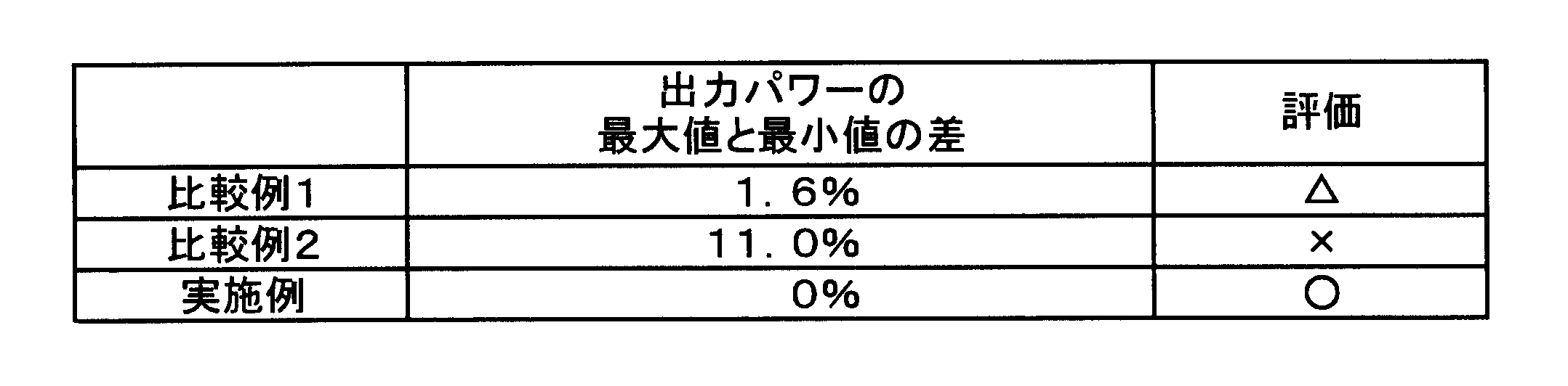
表1に示すように、最も変化が大きかったものは、比較例2であり、最大値と最小値の差は11.0%であった。また、次に変化が大きかったものは、比較例1であり、最大値と最小値の差は1.6%であった。一方、実施例は、最大値と最小値の差が無く、振動に最も強い結果となった。これは、比較例2の場合、落下による振動や落下の衝撃による保持ケース33の変形によって、入射側光ファイバ10と出射側光ファイバ21との間40の光結合がずれたことが原因で、光が損失したためと考えられる。それに対して、実施例および比較例1は、入射側光ファイバ10と出射側光ファイバ21との間40が保持部材32のほぼ中央に位置しているため、落下による振動でも光結合がずれにくく、落下の衝撃で保持ケース33が変形した場合でも、保持部材32に対する影響を少なくすることができる。さらに、実施例の場合は、入射側光ファイバ10と出射側光ファイバ21との間40に保護媒体50が介在されているため、落下による振動や落下の衝撃で保持ケース33が変形した場合でも、光結合がさらにずれにくく、良好な透過特性を保つことができると考えられる。
次に、実施例および比較例3を用いて、透過特性を比較する。ここで、比較例3における光デバイスが、実施例に係る光デバイス1と異なる所は、複数の入射側光ファイバ10同士を接着固定する接着剤55が異なるところである。具体的に、実施例に用いられる接着剤55は、波長400nmでの透過率が87%以上で、かつガラス転移温度230℃以上、ショア硬さが88の特性を有する。一方、比較例3に用いられる接着剤は、通信などで一般的に用いられているエポテック社製の熱硬化型接着剤353NDであり、その特性は、波長550nmでの透過率50%以上、ガラス転移温度90℃以上、ショア硬さが85である。実施例に用いられる接着剤55と比較例3に用いられるエポテック社製353NDの透過特性を図10に示す。
図10(a)に示す比較例3に用いられるエポテック社製353NDの透過特性と、図10(b)に示す実施例に用いられる接着剤55の透過特性と、を比較すると、特に近紫外域での透過特性に差があることが分かる。具体的には、比較例3に用いられるエポテック社製353NDの場合、約500nm以下の波長帯域では透過率が0%であり、全く光を透過させないことが分かる。一方、実施例に用いられる接着剤55の場合、500nmの波長でも90%の透過率があり、約250nm以下の波長帯域になるまで透過率が0%にはならない。つまり、実施例に用いられる接着剤55は、エポテック社製353NDに比べて、近紫外域での透過特性が良好であることが分かる。
上記のように、エポテック社製353NDを用いた比較例3と、接着剤55を用いた実施例と、に2Wのパワーの光を透過させた時の10時間経過後の透過率の低下を表2に示す。
表2に示すように、比較例3については、10時間経過後に透過率が2%低下している。一方、実施例については、10時間経過しても透過率は低下しない。これは、実施例に用いられる接着剤55は、比較例3に用いられるエポテック社製353NDよりも耐熱性に優れていることに起因すると考えられる。具体的には、エポテック社製353NDのガラス転移温度は90℃以上であるが、接着剤55のガラス転移温度は230℃以上と高い耐熱性を有する。ここで、入射側光ファイバ10はマルチモード光ファイバであり、束ねられた4本の入射側光ファイバ10同士の間にできる隙間には、多量の接着剤で埋められている。そのため、隙間に充填される接着剤の耐熱性が低いと、クラッド層の薄いマルチモード光ファイバから漏れた光による発熱で接着剤が劣化して、その一部が保護媒体50に付着する恐れがある。そして、付着した接着剤の一部によって透過特性を劣化させることがある。エポテック社製353NDよりも耐熱性に優れた接着剤55を用いた実施例の場合は、クラッド層が薄くて光を漏えいしやすいマルチモード光ファイバを用いた場合でも、漏えいした光の吸収による発熱で接着剤55の劣化が起こりにくい。そのため、接着剤55の劣化によって剥がれ落ちた一部の接着剤55が保護媒体50に付着することで透過率の低下を引き起こしてしまうことがない。さらに、実施例に用いられる接着剤55は、比較例3に用いられるエポテック社製353NDよりも透過率が高いことも結果に関係していると考えられる。つまり、比較例3の接着剤のように透過率が低いと、接着剤が光を吸収することによる温度上昇によって接着剤の劣化を早めてしまうが、実施例の接着剤55は、エポテック社製353NDよりも透過率が高いため、劣化しにくい。これにより、透過特性の良好な光デバイス1を提供することができる。
(本実施形態の概要)
以上のように、本実施形態に係る光デバイス1は、入射された光を出射端面から出射する入射側光ファイバ10と、出射端面から出射された光を出射端面と対向する入射端面から入射する出射側光ファイバ21と、出射端面と入射端面との間40に介在し、出射端面から出射された光を入射端面へ透過させるゲル状の樹脂57からなる保護媒体50と、を備えている。
以上のように、本実施形態に係る光デバイス1は、入射された光を出射端面から出射する入射側光ファイバ10と、出射端面から出射された光を出射端面と対向する入射端面から入射する出射側光ファイバ21と、出射端面と入射端面との間40に介在し、出射端面から出射された光を入射端面へ透過させるゲル状の樹脂57からなる保護媒体50と、を備えている。
上記の構成によれば、入射側光ファイバ10の出射端面と出射側光ファイバ21の入射端面との間40にゲル状の樹脂57からなる保護媒体50が介在している。そのため、振動などによって入射側光ファイバ10および出射側光ファイバ21の端面同士がこすれたり、入射側光ファイバ10の出射端面と出射側光ファイバ21の入射端面との間40に掛かる圧着荷重が大きくなったりした場合でも、保護媒体50自体が損傷することがない。これにより、保護媒体50の損傷が原因による光デバイス1の透過特性の劣化を防止することができる。
また、本実施形態に係る光デバイス1において、保護媒体50が、シリコーンからなるゲル状の樹脂57である。
上記の構成によれば、保護媒体50が、入射側光ファイバ10および出射側光ファイバ21との屈折率差が小さいシリコーンから構成されるため、透過特性の良好な光デバイス1を提供することができる。また、シリコーンは耐熱性に優れているため、温度上昇した場合でも保護媒体50が変質しにくく、耐光性にも優れているため、保護媒体50の屈折率や透過率が変化しにくい。そのため、良好な透過特性を有する光デバイス1を提供することができる。
また、本実施形態に係る光デバイス1において、入射側光ファイバ10が、マルチモード光ファイバである。
上記の構成によれば、光源30a・30b・30c・30dとの接続が容易で、発光面積の大きいハイパワー光源にも接続できる光デバイス1を提供することができる。
また、本実施形態に係る光デバイス1において、複数の入射側光ファイバ10が束ねられている。
上記の構成によれば、同波長や異なる波長、また異なる出力パワーの光などを結合する光デバイス1を提供することができる。
また、本実施形態に係る光デバイス1において、入射側光ファイバ10の出射端面が、平面状に研磨されている。
上記の構成によれば、平面状に研磨されていない場合に比べて、入射側光ファイバ10の出射端面から出射された光は、真っ直ぐに出射側光ファイバ21の入射端面へ伝送される。これにより、入射側光ファイバ10からの光を出射側光ファイバ21内へ低損失で伝送することができる。
また、本実施形態に係る光デバイス1において、複数の入射側光ファイバ10同士を接着固定する接着剤55が、波長400nmでの透過率が50%以上で、かつガラス転移温度が130℃以上である。
上記の構成によれば、例えばクラッド層が薄くて光を漏えいしやすいマルチモード光ファイバを用いた場合でも、漏えいした光の吸収による発熱で接着剤の劣化が起こりにくい。そのため、接着剤の劣化によって剥がれ落ちた一部の接着剤が保護媒体50に付着することで透過率の低下を引き起こしてしまうことがない。これにより、透過特性の良好な光デバイスを提供することができる。
また、本実施形態に係る光デバイス1は、入射側光ファイバ10を収納する入射側光学部材13と、出射側光ファイバ21を収納する出射側光学部材23と、入射側光ファイバ10の出射端面と出射側光ファイバ21の入射端面とを対向させるように、入射側光学部材13と出射側光学部材23とを保持する保持部材32と、入射側光学部材13と出射側光学部材23と保持部材32とを一体的に収納する保持ケース33と、を備え、保持部材32は、保持ケース33に接触されることなく保持ケース33内に収納されている。
上記の構成によれば、入射側光学部材13と出射側光学部材23とを保持する保持部材32が保持ケース33に接触されずに収納されている。従って、漏れ光が空気中に放出されるため、漏れ光が保持部材32に再吸収されにくく、保持部材32の温度上昇を防ぐことができる。さらに、保持ケース33内の温度上昇によって保持ケース33が変形した場合でも、保持部材32に対する影響を少なくすることができる。
また、本実施形態に係る光デバイス1の製造方法は、入射された光を出射端面から出射する入射側光ファイバ10と、出射端面から出射された光を出射端面と対向する入射端面から入射する出射側光ファイバ21と、を備えた光デバイス1の製造方法であって、出射端面および入射端面の何れか一方にゲル状の樹脂57を粘着し、他方を樹脂57に圧着させて、出射端面と入射端面との間40に保護媒体50を形成する。
上記の製造方法によれば、入射側光ファイバ10の出射端面と出射側光ファイバ21の入射端面との間40にゲル状の樹脂57からなる保護媒体50を形成することができる。そのため、振動などによって入射側光ファイバ10および出射側光ファイバ21の端面同士がこすれたり、入射側光ファイバ10の出射端面と出射側光ファイバ21の入射端面との間40に掛かる圧着荷重が大きくなったりした場合でも、保護媒体50自体が損傷することがない。これにより、保護媒体50の損傷が原因による光デバイス1の透過特性の劣化を防止することができる。また、保護媒体50に用いられる樹脂57は流動性のないゲル状であるため、入射側光ファイバ10の出射端面および出射側光ファイバ21の入射端面への粘着が容易であり、作業効率が良い。さらに、粘着した樹脂57に他方の端面を圧着させるだけで保護媒体50を形成できるため、蒸着法やイオンアシスト法などで膜を形成するよりも短時間で容易に保護媒体50を形成することができる。
以上、本発明の一実施形態を説明した。なお、本発明は上記の実施形態に限定される必要はない。
例えば、本実施形態に係る光デバイス1において、保護媒体50に使用されるゲル状の樹脂57は、予め脱気された状態で、使用されていてもよい。この場合、ゲル状の樹脂57に内在する気泡(空気)によって、光結合の際に光が反射されることがないため、より透過特性の良好な光デバイス1を提供することができる。
また、本実施形態に係る光デバイス1において、保持ケース33内にヒートシンクなどの放熱部材が設けられていてもよい。この場合、保持ケース33内で発生した熱が放熱部材によって放熱されやすくなるため、発熱による接着剤55の劣化や保持ケース33の変形による光結合のずれなどを防止することができる。従って、より透過特性の良好な光デバイス1を提供することができる。
以上、本発明の実施例を説明したが、具体例を例示したに過ぎず、特に本発明を限定するものではなく、具体的構成などは、適宜設計変更可能である。また、発明の実施形態に記載された、作用および効果は、本発明から生じる最も好適な作用および効果を列挙したに過ぎず、本発明による作用および効果は、本発明の実施形態に記載されたものに限定されるものではない。
本発明は、光ファイバの端面同士を対向させて光結合させる光デバイスについて利用することができる。
1 光デバイス
10 入射側光ファイバ
12 保護チューブ
13 入射側光学部材
14 フランジ
15 キャピラリ
16 先端フェルール
21 出射側光ファイバ
22 保護チューブ
23 入射側光学部材
24 フランジ
25 キャピラリ
26 先端フェルール
30a 光源
30b 光源
30c 光源
30d 光源
32 保持部材
33 保持ケース
34 バネ
35 拡大部
40 入射側光ファイバと出射側光ファイバとの間
50 保護媒体
10 入射側光ファイバ
12 保護チューブ
13 入射側光学部材
14 フランジ
15 キャピラリ
16 先端フェルール
21 出射側光ファイバ
22 保護チューブ
23 入射側光学部材
24 フランジ
25 キャピラリ
26 先端フェルール
30a 光源
30b 光源
30c 光源
30d 光源
32 保持部材
33 保持ケース
34 バネ
35 拡大部
40 入射側光ファイバと出射側光ファイバとの間
50 保護媒体
Claims (8)
- 入射された光を出射端面から出射する入射側光ファイバと、
前記出射端面から出射された前記光を当該出射端面と対向する入射端面から入射する出射側光ファイバと、
前記出射端面と前記入射端面との間に介在し、当該出射端面から出射された前記光を前記入射端面へ透過させるゲル状の樹脂からなる保護媒体と、
を備えたことを特徴とする光デバイス。 - 前記保護媒体が、シリコーンからなるゲル状の樹脂であることを特徴とする請求項1に記載の光デバイス。
- 前記入射側光ファイバが、マルチモード光ファイバであることを特徴とする請求項1に記載の光デバイス。
- 複数の前記入射側光ファイバが束ねられていることを特徴とする請求項1に記載の光デバイス。
- 前記入射側光ファイバの前記出射端面が、平面状に研磨されていることを特徴とする請求項1に記載の光デバイス。
- 前記複数の入射側光ファイバ同士を接着固定する接着剤が、波長400nmでの透過率が50%以上で、かつガラス転移温度が130℃以上であることを特徴とする請求項4に記載の光デバイス。
- 前記入射側光ファイバを収納する入射側光学部材と、
前記出射側光ファイバを収納する出射側光学部材と、
前記入射側光ファイバの出射端面と前記出射側光ファイバの入射端面とを対向させるように、前記入射側光学部材と前記出射側光学部材とを保持する保持部材と、
当該入射側光学部材と当該出射側光学部材と当該保持部材とを一体的に収納する保持ケースと、を備え、
前記保持部材は、前記保持ケースに接触されることなく当該保持ケース内に収納されていることを特徴とする請求項1ないし6の何れか1項に記載の光デバイス。 - 入射された光を出射端面から出射する入射側光ファイバと、当該出射端面から出射された当該光を当該出射端面と対向する入射端面から入射する出射側光ファイバと、を備えた光デバイスの製造方法であって、
前記出射端面および前記入射端面の何れか一方にゲル状の樹脂を粘着し、他方を当該樹脂に圧着させて、当該出射端面と当該入射端面との間に保護媒体を形成することを特徴とする光デバイスの製造方法。
Applications Claiming Priority (2)
| Application Number | Priority Date | Filing Date | Title |
|---|---|---|---|
| JP2010-133617 | 2010-06-11 | ||
| JP2010133617A JP5637740B2 (ja) | 2010-06-11 | 2010-06-11 | 光デバイスおよび光デバイスの製造方法。 |
Publications (1)
| Publication Number | Publication Date |
|---|---|
| WO2011155342A1 true WO2011155342A1 (ja) | 2011-12-15 |
Family
ID=45097950
Family Applications (1)
| Application Number | Title | Priority Date | Filing Date |
|---|---|---|---|
| PCT/JP2011/062118 Ceased WO2011155342A1 (ja) | 2010-06-11 | 2011-05-26 | 光デバイスおよび光デバイスの製造方法 |
Country Status (2)
| Country | Link |
|---|---|
| JP (1) | JP5637740B2 (ja) |
| WO (1) | WO2011155342A1 (ja) |
Citations (1)
| Publication number | Priority date | Publication date | Assignee | Title |
|---|---|---|---|---|
| WO2001088584A1 (fr) * | 2000-05-12 | 2001-11-22 | Takeo Inagaki | Connecteur de fibres optiques |
Family Cites Families (6)
| Publication number | Priority date | Publication date | Assignee | Title |
|---|---|---|---|---|
| JPH10111429A (ja) * | 1996-10-07 | 1998-04-28 | Yasuhiro Koike | 光伝送体の接続構造 |
| JP2006011119A (ja) * | 2004-06-28 | 2006-01-12 | Fujikura Ltd | 光部品、波長合分波器および光部品の製造方法 |
| JP4762833B2 (ja) * | 2006-09-05 | 2011-08-31 | 浜松ホトニクス株式会社 | 光学部品 |
| JP2008124358A (ja) * | 2006-11-15 | 2008-05-29 | Sumitomo Electric Ind Ltd | レーザモジュール |
| JP2008216506A (ja) * | 2007-03-01 | 2008-09-18 | National Institute Of Advanced Industrial & Technology | 光源装置 |
| JP4856673B2 (ja) * | 2008-05-15 | 2012-01-18 | 日立電線株式会社 | 通信光検知器 |
-
2010
- 2010-06-11 JP JP2010133617A patent/JP5637740B2/ja active Active
-
2011
- 2011-05-26 WO PCT/JP2011/062118 patent/WO2011155342A1/ja not_active Ceased
Patent Citations (1)
| Publication number | Priority date | Publication date | Assignee | Title |
|---|---|---|---|---|
| WO2001088584A1 (fr) * | 2000-05-12 | 2001-11-22 | Takeo Inagaki | Connecteur de fibres optiques |
Also Published As
| Publication number | Publication date |
|---|---|
| JP5637740B2 (ja) | 2014-12-10 |
| JP2011257665A (ja) | 2011-12-22 |
Similar Documents
| Publication | Publication Date | Title |
|---|---|---|
| CN105659133B (zh) | 光电子组件 | |
| TW594093B (en) | Optical transmission and reception system, and optical transmission and reception module and optical cable for the system | |
| US8142082B2 (en) | Optical assembly optically coupling an optical fiber and a semiconductor device | |
| US9874671B2 (en) | Light diffusing fiber lighting device | |
| JP2017520924A (ja) | 単レンズを有する光拡散ファイバー点灯装置 | |
| JP5750997B2 (ja) | 光コネクタモジュール | |
| EP3130951B1 (en) | Optical fiber assembly, optical coupling device, and optical fiber coupling device | |
| WO2007116792A1 (ja) | 光学部品の光入出力端およびビーム変換装置 | |
| CN101666890A (zh) | 高功率光纤准直器及其制造方法 | |
| JP2007293300A (ja) | ビーム変換装置 | |
| JP5637740B2 (ja) | 光デバイスおよび光デバイスの製造方法。 | |
| JP2004126563A (ja) | レンズ一体型光ファイバとその製造方法 | |
| US20050053334A1 (en) | Photodetector/optical fiber apparatus with enhanced optical coupling efficiency and method for forming the same | |
| US20190033534A1 (en) | Optical fiber connector, optical apparatus, optical transceiver, and method of manufacturing optical fiber connector | |
| EP3376272B1 (en) | Housing for encapsulating light emitting module, and light emitting module | |
| US20230198220A1 (en) | Optical fiber support structure and semiconductor laser module | |
| JP7600616B2 (ja) | 光デバイス | |
| JP2010217236A (ja) | 光利得等化モジュール | |
| JP2010079256A (ja) | 光ファイバピグテイル | |
| JP2009109715A (ja) | ファイバスタブおよびこれを用いた光コネクタ部品、光モジュール | |
| JP2014194451A (ja) | 照光装置 | |
| WO2012046656A1 (ja) | 光源モジュール | |
| JP2008242418A (ja) | 光ファイバコリメータ、光デバイスおよびこれを用いた光送受信器 | |
| JP2008033015A (ja) | ファイバスタブとそれを用いた光レセプタクルならびに光モジュール | |
| JP2014010303A (ja) | 光モジュール |
Legal Events
| Date | Code | Title | Description |
|---|---|---|---|
| 121 | Ep: the epo has been informed by wipo that ep was designated in this application |
Ref document number: 11792299 Country of ref document: EP Kind code of ref document: A1 |
|
| NENP | Non-entry into the national phase |
Ref country code: DE |
|
| 122 | Ep: pct application non-entry in european phase |
Ref document number: 11792299 Country of ref document: EP Kind code of ref document: A1 |