WO2011145463A1 - アクチュエータの駆動装置および駆動方法 - Google Patents
アクチュエータの駆動装置および駆動方法 Download PDFInfo
- Publication number
- WO2011145463A1 WO2011145463A1 PCT/JP2011/060634 JP2011060634W WO2011145463A1 WO 2011145463 A1 WO2011145463 A1 WO 2011145463A1 JP 2011060634 W JP2011060634 W JP 2011060634W WO 2011145463 A1 WO2011145463 A1 WO 2011145463A1
- Authority
- WO
- WIPO (PCT)
- Prior art keywords
- constant current
- resistance value
- shape memory
- alloy wire
- memory alloy
- Prior art date
- Legal status (The legal status is an assumption and is not a legal conclusion. Google has not performed a legal analysis and makes no representation as to the accuracy of the status listed.)
- Ceased
Links
Images



Classifications
-
- F—MECHANICAL ENGINEERING; LIGHTING; HEATING; WEAPONS; BLASTING
- F03—MACHINES OR ENGINES FOR LIQUIDS; WIND, SPRING, OR WEIGHT MOTORS; PRODUCING MECHANICAL POWER OR A REACTIVE PROPULSIVE THRUST, NOT OTHERWISE PROVIDED FOR
- F03G—SPRING, WEIGHT, INERTIA OR LIKE MOTORS; MECHANICAL-POWER PRODUCING DEVICES OR MECHANISMS, NOT OTHERWISE PROVIDED FOR OR USING ENERGY SOURCES NOT OTHERWISE PROVIDED FOR
- F03G7/00—Mechanical-power-producing mechanisms, not otherwise provided for or using energy sources not otherwise provided for
- F03G7/06—Mechanical-power-producing mechanisms, not otherwise provided for or using energy sources not otherwise provided for using expansion or contraction of bodies due to heating, cooling, moistening, drying or the like
- F03G7/061—Mechanical-power-producing mechanisms, not otherwise provided for or using energy sources not otherwise provided for using expansion or contraction of bodies due to heating, cooling, moistening, drying or the like characterised by the actuating element
- F03G7/0614—Mechanical-power-producing mechanisms, not otherwise provided for or using energy sources not otherwise provided for using expansion or contraction of bodies due to heating, cooling, moistening, drying or the like characterised by the actuating element using shape memory elements
- F03G7/06143—Wires
-
- F—MECHANICAL ENGINEERING; LIGHTING; HEATING; WEAPONS; BLASTING
- F03—MACHINES OR ENGINES FOR LIQUIDS; WIND, SPRING, OR WEIGHT MOTORS; PRODUCING MECHANICAL POWER OR A REACTIVE PROPULSIVE THRUST, NOT OTHERWISE PROVIDED FOR
- F03G—SPRING, WEIGHT, INERTIA OR LIKE MOTORS; MECHANICAL-POWER PRODUCING DEVICES OR MECHANISMS, NOT OTHERWISE PROVIDED FOR OR USING ENERGY SOURCES NOT OTHERWISE PROVIDED FOR
- F03G7/00—Mechanical-power-producing mechanisms, not otherwise provided for or using energy sources not otherwise provided for
- F03G7/06—Mechanical-power-producing mechanisms, not otherwise provided for or using energy sources not otherwise provided for using expansion or contraction of bodies due to heating, cooling, moistening, drying or the like
- F03G7/066—Actuator control or monitoring
Definitions
- the present invention relates to a drive device for an actuator that drives a lens unit constituting an imaging optical system such as a mobile phone with a camera, and more particularly to a drive device for an actuator using a shape memory alloy and a drive method for the actuator.
- a lens driving device that moves the lens in the optical axis direction.
- a lens driving device using a shape memory alloy (SMA) as an actuator has been devised. Yes.
- SMA shape memory alloy
- This device heats the SMA by energizing it, generates a contraction force by heating, and uses the contraction force as a lens driving force. It is easy to reduce the size and weight, and has a relatively large driving force. There is an advantage that can be obtained.
- SMA also has a characteristic that its resistance value changes depending on the amount of contraction. Specifically, when the length is reduced by 1%, the resistance value is reduced by 5 to 6%. Therefore, when this is used as an actuator, there is an advantage that the position can be known without providing a position sensor for detecting the position of the driven object.
- the current position of the driven object driven by the actuator can be known by measuring the resistance value of SMA during driving.
- Patent Document 1 A technique for measuring the resistance value of the SMA and acquiring the current position of the driven object from the value is disclosed in Patent Document 1, for example.
- Patent Document 1 also discloses a technique for detecting the environmental temperature based on the resistance value of the SMA and changing the driving characteristics of the SMA based on the detected environmental temperature.
- the constant current (I) is applied to the SMA.
- a constant current circuit is suitable as an SMA drive circuit, and PWM (Pulse Width Modulation) control or the like is required to control the amount of current.
- actuators for small devices that use a battery such as a mobile phone as the power source often have a low power supply voltage of several volts, and it is required to keep power consumption lower.
- an appropriate constant current value has not been set for the resistance value of the SMA, and low power consumption has not been sufficiently achieved.
- the present invention has been made to solve the above-described problems.
- an appropriate constant current value can be set for the resistance value of SMA. It is an object of the present invention to provide an actuator drive device that can reduce power consumption. Another object of the present invention is to provide an actuator driving method that can set an appropriate constant current value for the resistance value of the SMA in the driving method of the actuator using the SMA and can further reduce power consumption.
- the shape memory alloy wire is formed of a shape memory alloy wire, and the shape memory alloy wire expands and contracts in response to heat generated by passing a current through the shape memory alloy wire.
- An actuator driving device that drives a driven object in conjunction with each other, detecting a constant current circuit that supplies a constant current to the shape memory alloy wire and a resistance value of the shape memory alloy wire when energized, and detecting A resistance value detection circuit for adjusting a constant current value flowing in the constant current circuit according to the resistance value, and a pulse signal modulated by a pulse width modulation based on a potential difference between both ends of the shape memory alloy wire.
- a pulse width modulation circuit for performing on / off control of a current source transistor, wherein the resistance value detection circuit is configured to control the constant current with respect to the magnitude of the resistance value of the shape memory alloy wire. Magnitude relationship values to adjust the constant current value so that the opposite.
- the constant current circuit has a resistance element connected in series to the current source transistor, and a voltage generated in the resistance element is equal to a reference voltage.
- a comparator for performing feedback control, the shape memory alloy wire is interposed between the resistance element and the current source transistor, and the resistance value detection circuit is configured to adjust the resistance value of the shape memory alloy wire. Based on this, the constant current value of the constant current circuit is adjusted by changing the voltage value of the reference voltage applied to the comparator.
- the detection of the resistance value of the shape memory alloy wire is executed as an initial operation, and the resistance value detection circuit is configured to detect the resistance value of the shape memory alloy wire.
- the resistance value measurement voltage smaller than the voltage value for driving the driven object is applied to the comparator as the reference voltage, thereby energizing the shape memory alloy wire and the resistance value. Is detected.
- the resistance value detection circuit is configured such that the relationship of the magnitude of the constant current value with respect to the magnitude of the resistance value of the shape memory alloy wire is reversed. The voltage value of the voltage is changed.
- the shape memory alloy wire is formed of a shape memory alloy wire, and the shape memory alloy wire expands and contracts in response to heat generated by passing a current through the shape memory alloy wire.
- a driving apparatus for an actuator that drives a driven object in conjunction with each other, and holds a constant current circuit that supplies a constant current to the shape memory alloy wire and data relating to a resistance value of the shape memory alloy wire when energized.
- Pulse width modulation based on a memory unit, a current adjustment circuit that adjusts a constant current value flowing in the constant current circuit according to the resistance value held in the memory unit, and a potential difference between both ends of the shape memory alloy wire
- a pulse width modulation circuit that performs on / off control of the current source transistor of the constant current circuit according to the pulse signal, and the current adjustment circuit includes a power consumption of the constant current circuit. It said adjusting the constant current value to reduce.
- a first aspect of the actuator driving method is an actuator driving method for driving a driven object by expanding and contracting the shape memory alloy wire by flowing current from the constant current circuit to the shape memory alloy wire. Detecting a resistance value of the shape memory alloy wire during energization, adjusting a constant current value flowing through the constant current circuit in accordance with the detected resistance value (b), And (c) pulse width modulating the current supplied to the shape memory alloy wire based on a potential difference between both ends of the shape memory alloy wire, wherein the step (b) Adjusting the constant current value so that the relationship between the magnitude of the resistance value and the magnitude of the constant current value is opposite.
- the step (a) includes a step of energizing the shape memory alloy wire with a current that does not cause the shape memory alloy wire to contract.
- the resistance value detection circuit has a constant current value such that the relationship between the magnitude of the constant current value with respect to the magnitude of the resistance value of the shape memory alloy wire is reversed. Therefore, the reactive power in the current source transistor can be reduced, the power consumption efficiency can be improved, and a further reduction in power consumption can be achieved.
- the actuator drive device of the present invention it is possible to prevent the actuator from generating heat and contracting when detecting the resistance value of the shape memory alloy wire.
- the constant current value is reduced when the resistance value of the shape memory alloy wire is large, and the constant current when the resistance value of the shape memory alloy wire is small. Since the value is increased, the reactive power in the current source transistor can be reduced and the power consumption efficiency can be improved.
- the current adjustment circuit flows to the constant current circuit according to the resistance value held in the storage unit so as to reduce the power consumption of the constant current circuit. Since the constant current value is adjusted, the reactive power in the current source transistor can be reduced, the power consumption efficiency can be improved, and a further reduction in power consumption can be achieved.
- the constant current value is adjusted so that the relationship between the magnitude of the constant current value and the magnitude of the resistance value of the shape memory alloy wire is reversed. Reactive power in the source transistor can be reduced to improve power consumption efficiency, and further reduction in power consumption can be achieved.
- a current that does not contract the shape memory alloy wire is supplied to the shape memory alloy wire.
- the resistance value of the shape memory alloy wire in a state where the alloy wire does not contract can be measured.
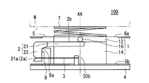
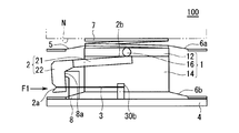
- FIG. 1 and 2 schematically show the main components of a lens driving device 100 using an SMA actuator as a driving source
- FIG. 1 is a plan view seen from the lens side
- FIG. 3 shows a side view seen from the direction of arrow A in FIG. 2 shows a state before driving
- FIG. 3 shows a state after driving.
- the lens driving device 100 mainly includes a lens unit 1 (driven object), a lever member 2 that moves the lens unit 1 in the optical axis AX direction (first axial direction), an SMA actuator 3, a base member 4, a ceiling member.
- a plate 5, parallel plate springs 6 a and 6 b, a bias spring 7, and the like are provided, and the lens unit 1 and the like are assembled to the base member 4.
- the top plate 5 and the parallel leaf springs 6a and 6b are omitted in FIG. 1 for convenience.
- the base member 4 is fixed to a member to be attached to the lens driving device 100 (for example, a frame of a mobile phone, a mount substrate, etc.), and is a non-moving member constituting the bottom side of the lens driving device 100.
- the base member 4 is formed in a square plate shape in plan view, and is entirely made of a resin material or the like.
- the lens unit 1 has a cylindrical shape, and includes an imaging lens 10, a lens driving frame 12 that holds the imaging lens 10, and a lens barrel 14 that stores the lens driving frame 12.
- the imaging lens 10 includes an objective lens, a focus lens, a zoom lens, and the like, and constitutes an imaging optical system for a subject image with respect to an imaging element (not shown).
- the lens driving frame 12 is a so-called ball frame, and moves in the optical axis AX direction together with the lens barrel 14.
- a pair of support portions 16 project from the outer peripheral edge portion of the lens drive frame 12 at the distal end on the object side with an angular difference of 180 ° in the circumferential direction.
- the lens unit 1 is disposed on the base member 4 in a state of being inserted into an opening formed in the top plate 5.
- the pair of support portions 16 are arranged so as to be positioned in the vicinity of the pair of diagonals of the base member 4 (see FIG. 1).
- Parallel plate springs 6a and 6b are fixed to the base member 4 and the top plate 5, respectively, and the lens unit 1 is fixed to the parallel plate springs 6a and 6b. Accordingly, the lens unit 1 is supported so as to be displaceable with respect to the base member 4 and the like, and the degree of freedom of displacement is restricted in a direction along the optical axis AX.
- the top plate 5 may be fixed to the base member 4 via a support column (not shown) or may be a structure integrated with the base member 4.
- the lever member 2 applies a driving force in the direction of the optical axis AX to the lens unit 1 by engaging with the lens unit 1 via the support portion 16.
- the lever member 2 is disposed on the side of the lens unit 1, specifically, at one corner other than the corner where the support portion 16 of the lens unit 1 is located, which is the corner of the base member 4. .
- the lever member 2 is supported so as to be swingable about an axis that is orthogonal to the optical axis AX and extends in the direction in which the pair of support portions 16 are arranged (the vertical direction in FIG. 1).
- the lever member 2 has an inverted L-shape in a side view including an arm portion 21 and an extending portion 22 extending from the base end portion of the arm portion 21 in the optical axis AX direction.
- a bent portion serving as a boundary between the arm portion 21 and the extending portion 22 is supported on the base member 4 by being supported by the tip of the support leg 8 erected on the base member 4.
- the shape of the tip of the support leg 8 (hereinafter referred to as the lever support portion 8a) is a substantially cylindrical shape extending in a direction perpendicular to the optical axis AX direction (direction perpendicular to the paper surface of FIG. 2).
- the lever member 2 is supported so as to be swingable about an axis orthogonal to the optical axis AX direction with the lever support portion 8a as a fulcrum.
- the arm portion 21 is formed in an arc shape in plan view. Specifically, as shown in FIG. 1, the lens unit 1 is bifurcated from the extended portion 22 to both sides of the lens unit 1 and extends evenly in the vicinity of the outer peripheral surface of the lens unit 1. Is formed so as to surround. The tips (both ends) of the arm portion 21 reach the positions of the support portions 16 of the lens unit 1, respectively. Then, the SMA actuator 3 is bridged over the extended portion 22, and the moving force in a direction perpendicular to the optical axis AX direction (second axis direction: left-right direction in FIG. 2) at this bridging position (referred to as the displacement input portion 2 a). When F1 (see FIG. 3) is input, the lever member 2 swings.
- the tip of the arm portion 21 (referred to as the displacement output portion 2b) is displaced in the optical axis AX direction, and the displacement output portion 2b engages with each support portion 16 to cause the lens unit 1 to move in the optical axis AX direction.
- a driving force is applied.
- the SMA actuator 3 applies a moving force F1 (see FIG. 3) to the lever member 2, and is a linear actuator made of SMA wire such as Ni—Ti alloy.
- the SMA actuator 3 expands when given a predetermined tension in a state where the elastic modulus is low (martensite phase) at a low temperature. When heat is applied in this extended state, the SMA actuator 3 undergoes phase transformation and has a high elastic modulus (austenite). Phase: parent phase) and return to its original length from its extended state (recover shape).
- the SMA actuator 3 is energized and heated to perform the above-described phase transformation. That is, since the SMA actuator 3 is a conductor having a predetermined resistance value, Joule heat is generated by energizing the SMA actuator 3 itself, and transformation from the martensite phase to the austenite phase is performed by self-heating based on the Joule heat. It is supposed to be configured. For this reason, the first electrode 30 a and the second electrode 30 b for energization heating are fixed to both ends of the SMA actuator 3. These electrodes 30 a and 30 b are fixed to predetermined electrode fixing portions provided on the base member 4.
- the SMA actuator 3 is bridged between the electrodes 30a and 30b with a portion engaging with the extending portion 22 of the lever member 2 as a turning point.
- the SMA actuator 3 is energized and heated via the electrodes 30a and 30b and is operated (shrinks)
- the lever member 2 is given a moving force F1 (see FIG. 3), and the moving force F1 causes the lever member to move. 2 will swing.
- the electrodes 30a and 30b are arranged in the vicinity of the support portion 16 of the lens unit 1 in the base member 4, respectively.
- the lengths of the SMA actuator 3 from the electrodes 30a and 30b to the turn-back point are set to be equal to each other, so that the amount of expansion / contraction of the SMA actuator 3 on both sides of the displacement input portion 2a becomes equal. Rubbing between the lever member 2 and the SMA actuator 3 is prevented.
- a V-groove 21a (corresponding to the displacement input portion 2a) is formed in the extended portion 22, and the SMA actuator 3 is bridged so as to be fitted into the V-groove 21a, whereby the lever member 2 is On the other hand, the SMA actuator 3 is stably suspended.
- the bias spring 7 biases the lens unit 1 in the direction of the optical axis AX in the direction opposite to the direction in which the displacement output unit 2b moves due to the operation (contraction) of the SMA actuator 3.
- the bias spring 7 is formed of a compression coil spring having a diameter substantially matching the peripheral size of the lens drive frame 12, and one end side (lower end side) is in contact with the top surface of the lens drive frame 12. The other end side (upper end side) of the bias spring 7 is brought into contact with a non-moving portion N such as an inner surface of a housing of a mobile phone.
- the line length is set so that the SMA actuator 3 receives tension from the bias spring 7 acting via the lens unit 1 (support portion 16) and the lever member 2 and is tensioned. ing. That is, the line length is set so that the lever member 2 (arm portion 21) is always brought into contact (pressure contact) with the lens unit 1 (support portion 16) regardless of the operating state.
- the lever member 2 is swingably supported at the tip of the support leg 8 without directly connecting the support leg 8 and the lever member 2, and when the SMA actuator 3 is operated. The lever member 2 is swung by quickly transmitting the displacement.
- the constant current circuit is suitable as the driving circuit for the SMA.
- FIG. 4 shows an example of the configuration of a general constant current circuit.
- a PNP transistor 101 current source transistor
- an SMA actuator 3 resistance value R SMA
- a PNP transistor 101 current source transistor
- an SMA actuator 3 resistance value R SMA
- Vcc power supply voltage
- a resistor R1 are connected in series.
- the SMA actuator 3 corresponds to the SMA actuator 3 of the lens driving device 100 shown in FIGS.
- connection node between the SMA actuator 3 and the resistor R1 is connected to the non-inverting input (+) of the comparator 102, and the output of the comparator 102 is connected to the base of the PNP transistor 101 via the resistor R2. Further, the reference voltage Vr is applied to the inverting input ( ⁇ ) of the comparator 102.
- the potential difference between both ends of the SMA actuator 3 is amplified by a differential amplifier (not shown) and applied to the PWM control circuit, but is not shown for simplicity.
- the voltage Va is preferably close to the power supply voltage Vcc. That is, the power represented by the product of the voltage difference between the voltage Va and the power supply voltage Vcc and the constant current I becomes the collector loss of the PNP transistor 101 and is consumed as invalid heat.
- the optimum constant current I can be adjusted or selected in accordance with the variation of the resistance value RSMA of the SMA actuator 3, and the reactive power is reduced by reducing the reactive power by bringing the voltage Va as close to the power supply voltage Vcc as possible. Is the technical idea of the present invention.
- a PNP transistor 101 current source transistor
- an SMA actuator 3 resistance value R SMA
- a PNP transistor 101 current source transistor
- an SMA actuator 3 resistance value R SMA
- Vcc power supply voltage
- a resistor R1 are connected in series.
- the SMA actuator 3 corresponds to the SMA actuator 3 of the lens driving device 100 shown in FIGS.
- connection node between the SMA actuator 3 and the resistor R1 is connected to the non-inverting input (+) of the comparator 102, and the output of the comparator 102 is connected to the base of the PNP transistor 101 via the resistor R2 and the switch circuit 106. ing. Further, the reference voltage Vr is applied to the inverting input ( ⁇ ) of the comparator 102.
- the potential on the PNP transistor 101 side of the SMA actuator 3 is applied to the non-inverting input (+) of the differential amplifier 104, and the potential on the resistance R1 side of the SMA actuator 3 is applied to the inverting input ( ⁇ ) of the differential amplifier 104. It is a given configuration.
- the output of the differential amplifier 104 is provided to the sample hold circuit 107 and the resistance value detection circuit 111.
- the sample hold circuit 107 has a potential difference between both ends of the SMA actuator 3 amplified by the differential amplifier 104 during a period in which a pulse in PWM control is on (on pulse period), that is, a period in which a constant current is supplied. This is a circuit that samples a voltage and outputs the voltage while holding the pulse in the PWM control during the off period.
- the held voltage output from the sample hold circuit 107 is applied to the non-inverting input (+) of the differential amplifier 109. Further, the inverting input ( ⁇ ) of the differential amplifier 109 is configured to be supplied with the target position voltage output from the target position voltage setting circuit 108, and the output of the differential amplifier 109 is subjected to pulse width modulation (PWM). ) Is provided to the circuit 110.
- PWM pulse width modulation
- the pulse width modulation circuit 110 supplies a pulse signal that has been subjected to pulse width modulation based on the output of the differential amplifier 109 to the switch circuit 106, and performs on / off control of the PNP transistor 101 based on the pulse signal that has been subjected to pulse width modulation. .
- the resistance value detection circuit 111 detects the resistance value R SMA of the SMA actuator 3 based on the output of the differential amplifier 104, a reference voltage corresponding to the detected resistance value set by the reference voltage setting circuit 105, This is a circuit for giving to the inverting input ( ⁇ ) of the comparator 102.
- the reference voltage setting circuit 105 shown in FIG. 5 is configured to select a reference voltage from a plurality of predetermined reference voltages (Vr0 to Vr4), but is not limited to this. There is no limit to the number of reference voltage stages, and the voltage can be continuously varied steplessly.
- the target position voltage setting circuit 108 When the lens driving device 100 is used in a camera of a mobile phone, when the camera is turned on in step S1, the target position voltage setting circuit 108 immediately focuses on the initial target position set in advance or the subject. A target position for determining the target position is determined, a voltage corresponding to the target position is set, and output as a target position voltage (step S2).
- the resistance value detection circuit 111 selects and outputs a reference voltage Vr0 for resistance value measurement at the beginning of activation (step S3).
- This reference voltage Vr0 is set lower than the reference voltages Vr1 to Vr4 at the time of steady operation.
- the constant current circuit causes a constant current determined by the reference voltage Vr0 and the resistor R1 to flow through the SMA actuator 3, and the differential amplifier 104 amplifies the voltage at both ends of the SMA actuator 3 at this time to thereby detect the resistance value detection circuit 111. And output to the sample hold circuit 107.
- Resistance value detection circuit 111 detects the resistance value R SMA based on a voltage across the SMA actuator 3 (step S4), and a reference voltage corresponding to the detected resistance value is selected from among the reference voltages Vr1 ⁇ Vr4 (Step S5).
- the reference voltages Vr1 to Vr4 are such that the voltage Va (FIG. 5) becomes a value close to the power supply voltage Vcc so that the collector loss in the PNP transistor 101 can be reduced and the power loss in the constant current circuit can be optimized.
- the resistance value RSMA are prepared in advance according to the resistance value RSMA .
- the reference voltage Vr1 ⁇ Vr4 when the resistance value R SMA is relatively large value to reduce the constant current value is selected, the resistance value R SMA can be relatively small is selected values to increase the constant current value
- the reference voltage setting circuit 105 is controlled.
- a voltage corresponding to a standard resistance value (referred to as R ST ) serving as a standard for the SMA actuator 3 is selected from the reference voltages Vr1 to Vr4 and is referred to as a standard voltage (referred to as V ST). ).
- the detected resistance value R SMA is is greater than R ST, depending on the difference between R ST and R SMA, selects a smaller reference voltage than V ST.
- the reference voltage setting circuit 105 controls to select a reference voltage larger than V ST according to the difference between R ST and R SMA. Is done.
- the constant current circuit passes a constant current determined by the reference voltage Vrn (reference voltage selected based on a resistance value detected immediately after power-on) and the resistor R1 to the SMA actuator 3 (step S6), and the differential amplifier 104 At this time, the voltage at both ends of the SMA actuator 3 is amplified and output to the resistance value detection circuit 111 and the sample hold circuit 107 (step S7).
- Vrn reference voltage selected based on a resistance value detected immediately after power-on
- the sample hold circuit 107 holds the output of the differential amplifier 104 during a period in which a constant current is supplied and supplies the value to the differential amplifier 109, which is output from the target position voltage setting circuit 108. Comparison with the target position voltage is performed, and the difference is amplified and output (step S8).
- the pulse width modulation circuit 110 that has received the voltage difference between the output of the differential amplifier 104 and the target position voltage generates a pulse signal that has been subjected to pulse width modulation based on the difference, and supplies the pulse signal to the switch circuit 106, and the PNP transistor 101 is turned on / off (step S9).
- the SMA actuator 3 when the power is turned on, the SMA actuator 3 is naturally not contracted, and the potential difference between both ends of the SMA actuator 3 is higher than the target position voltage. This is due to the electrical characteristics of SMA.
- the pulse signal subjected to pulse width modulation has a long ON period, and a constant current flows through the SMA actuator 3 at a high rate. Due to this current, the SMA actuator 3 generates heat and starts to contract. When the SMA actuator 3 starts to contract, the lens unit 1 (FIG. 2) starts to move toward the target position.
- FIG. 7 shows the characteristic of the resistance value with respect to the driving amount in the autofocus operation of the lens unit 1 shown in FIGS.
- the horizontal axis shows the lens driving amount ( ⁇ m)
- the vertical axis shows the resistance value ( ⁇ )
- the characteristics when the environmental temperature is 60 ° C., 40 ° C., 20 ° C., 0 ° C. and ⁇ 20 ° C. are shown. ing.
- the resistance value decreases as the lens driving amount (shrinkage amount) increases, and that the resistance value increases as the environmental temperature increases.
- the resistance value of SMA changes with the amount of shrinkage and the environmental temperature.
- the SMA actuator 3 contracts, the resistance value decreases, and when the resistance value decreases, the potential difference between both ends of the SMA actuator 3 decreases and the difference from the target position voltage decreases. Accordingly, when the ON period of the pulse signal subjected to the pulse width modulation is shortened and the target position voltage becomes equal to the potential difference between both ends of the SMA actuator 3, the contraction of the SMA is stopped and the contracted state is maintained. As a result, the lens unit 1 stops near the target position.
- step S10 it is determined whether or not the target position voltage is to be changed.
- the lens driving is terminated, but when the target position voltage is changed, the target position voltage setting circuit 108 is changed. However, a new target position voltage is set, and the operations after step S7 are repeated.
- the output of the differential amplifier 109 changes, and the ON period of the pulse signal subjected to pulse width modulation also changes.
- the SMA actuator 3 further contracts or expands in the opposite direction, and the lens unit 1 moves.
- the contraction of the SMA stops and the contracted state is maintained. As a result, the lens unit 1 stops near the new target position.
- the target position voltage is changed in this manner in order to move the lens from the infinite position to the closest position in the AF (autofocus) sequence in the camera for mobile phones at step S7 and subsequent steps.
- the AF sequence is executed.
- the target position voltage in such an AF sequence is a value obtained by dividing the voltage corresponding to the infinite position to the voltage corresponding to the closest position by a predetermined number of steps.
- the predetermined reference voltage Vr0 is applied to the comparator 102, and a constant current determined by the reference voltage Vr0 and the resistor R1 is applied to the SMA.
- a configuration is adopted in which the voltage is applied to the actuator 3 and the voltage across the SMA actuator 3 at this time is detected.
- the resistance value detection circuit 111 detects a resistance value R SMA of the SMA actuator 3 based on the detected voltage, by setting a reference voltage corresponding to the detected resistance value, it adopts a configuration to provide to the comparator 102.
- the constant current value can be changed in accordance with the initial resistance value of the SMA actuator 3.
- the reference voltage to be set the terminal voltage of the SMA actuator 3, so that it can approach the power supply voltage Vcc as possible, by setting, based on the R SMA of the SMA actuator 3 as measured, PNP transistor 101 It is possible to reduce the reactive power and improve the power consumption efficiency.
- variable factors in the resistance value R SMA of the SMA actuator 3 1) SMA individual variation, 2) temperature, 3) time course and 4) 4 factors shrinkage is considered.
- the resistance value R SMA of the SMA actuator 3, 1), 2) and 3) will vary by 20% or more by three factors, is due to them 1) about 15%, 2 ) Is about 5% (temperature range of ⁇ 20 ° C. to 70 ° C.).
- the variation of the reference voltage is determined so as to cope with the variation of the resistance value in consideration of these variation factors.
- the reference voltage applied to the comparator 102 may be selected from a plurality of predetermined reference voltages as shown in FIG. 5, but may be changed continuously in a stepless manner. In this case, the above-described variation factors are taken into account when determining the variable range of the reference voltage.
- the constant current value of the constant current source be optimized based on the resistance value R SMA of the SMA actuator 3, it leads to the improvement of control capability of the PWM control.
- the SMA actuator 3 requires more power in the low temperature environment in order to obtain the same driving amount due to its characteristics, but the PWM control adjusts the power by changing the on-pulse width.
- the PWM control adjusts the power by changing the on-pulse width.
- the upper limit of power at this time is when the on-pulse width is 100%, but such a pulse is not realistic. Therefore, by optimizing the constant current value so as to increase the constant current value at low temperatures, the upper limit of the power can be made larger than when the constant current value is fixed.
- the SMA actuator 3 requires less power in the high temperature environment to obtain the same driving amount, and therefore the on-pulse width needs to be reduced.
- the on-pulse width becomes smaller than a certain limit, problems such as unstable operation occur. Therefore, by optimizing the constant current value so as to decrease the constant current value at a high temperature, the on-pulse width can be widened compared with the case where the constant current value is fixed, and the above-described problem is solved.
- the drive unit of the actuator described detects the resistance value R SMA based on a voltage across the SMA actuator 3 by the resistance value detection circuit 111, the reference voltage in the steady operation based on the detected resistance value R SMA
- the resistance value RSMA may be read from the storage device and the reference voltage may be set based on the value during steady operation.
- the resistance value detection circuit 111 the function of the resistance value detection is unnecessary, a reference voltage corresponding to the read out from the storage device resistance R SMA, as a current adjustment circuit for selecting from among the reference voltages Vr1 ⁇ Vr4 It suffices to have a configuration, and the configuration of the actuator drive device can be simplified.
- the set reference voltage can be set.
- SYMBOLS 1 Lens unit 2 Lever member 2a Displacement input part 2b Displacement output part 3 Shape memory alloy (SMA) actuator 4 Base member 6a, 6b Parallel leaf spring 8 Support leg 8a Lever support part 10 Imaging lens 100 Lens drive device
Landscapes
- Engineering & Computer Science (AREA)
- Chemical & Material Sciences (AREA)
- Combustion & Propulsion (AREA)
- Mechanical Engineering (AREA)
- General Engineering & Computer Science (AREA)
- Lens Barrels (AREA)
Abstract
本発明は、アクチュエータの駆動装置に関し、SMAワイヤに定電流を供給する定電流回路と、通電時のSMAワイヤの抵抗値を検出し、検出した抵抗値に応じて定電流回路に流れる定電流値を調整する抵抗値検出回路(111)と、SMAワイヤの両端の電位差に基づいて、パルス幅変調したパルス信号により定電流回路の電流源トランジスタのオン、オフ制御を行うパルス幅変調回路(110)とを備えている。
Description
本発明は、カメラ付き携帯電話等の撮像光学系を構成するレンズユニットを駆動するアクチュエータの駆動装置に関し、特に、形状記憶合金を用いたアクチュエータの駆動装置および該アクチュエータの駆動方法に関する。
近年、カメラ付き携帯電話機等に搭載される撮像素子の画素数が増大する等、高画質化が飛躍的に進んでおり、これに伴い、画像撮影という基本機能に加えて、フォーカス機能やズーム機能等を付加することが求められている。
これらの機能を付加するには、レンズを光軸方向に移動させるレンズ駆動装置が必要であり、最近では、形状記憶合金(Shape Memory Alloy:SMA)をアクチュエータに用いたレンズ駆動装置が考案されている。この装置は、SMAに通電するなどして加熱し、加熱による収縮力を発生させて、当該収縮力をレンズ駆動力として利用するもので、小型化、軽量化が容易かつ比較的大きな駆動力を得ることができるという利点がある。
また、SMAは、その抵抗値が収縮量によって変化するという特性がある。具体的には、長さが1%縮むと、抵抗値は5~6%小さくなるという特性を有している。従って、これをアクチュエータとして利用した場合、被駆動物の位置を検出するための位置センサーを設けずとも、その位置を知ることができるという利点も有している。
すなわち、SMAを用いたアクチュエータでは、駆動時のSMAの抵抗値を測定することにより、当該アクチュエータによって駆動する被駆動物の現在位置を知ることができる。
このように、SMAの抵抗値を測定して、その値から被駆動物の現在位置を取得する技術は、例えば特許文献1に開示されている。
この特許文献1においては、SMAの抵抗値に基づいて環境温度を検知したり、検知した環境温度により、SMAの駆動特性を変更する技術も開示されている。
以上説明したように、SMAの抵抗値を測定して、その値から被駆動物の現在位置を取得する技術は周知であり、SMAの抵抗値を測定するには、SMAに定電流(I)を流した時のSMA両端の電圧(V)を測定し、R=V/Iの式から抵抗値(R)を求める方法が最も簡単で一般的である。
従って、抵抗値を検出するという観点から、SMAの駆動回路としては定電流回路が適しており、その電流量を制御するためにはPWM(Pulse Width Modulation)制御等が必要となる。
一方、携帯電話等のバッテリーを電源とする小型機器のアクチュエータにおいては、電源電圧は数ボルトと低電圧のものが多く、消費電力をより低く抑えることが要求されている。しかしながら、これまでは、SMAの抵抗値に対して適切な定電流値が設定されておらず、低消費電力化が十分達成されていなかった。
本発明は上記のような問題点を解消するためになされたもので、SMAを用いたアクチュエータの駆動装置において、SMAの抵抗値に対して適切な定電流値を設定することができ、さらなる低消費電力化を可能とするアクチュエータの駆動装置を提供することを目的とする。また、SMAを用いたアクチュエータの駆動方法において、SMAの抵抗値に対して適切な定電流値を設定することができ、さらなる低消費電力化を可能とするアクチュエータの駆動方法を提供することを目的とする。
本発明に係るアクチュエータの駆動装置の第1の態様は、形状記憶合金ワイヤで構成され、該形状記憶合金ワイヤに電流を流すことで発生する熱に応じて前記形状記憶合金ワイヤが伸縮することに連動して、被駆動物を駆動するアクチュエータの駆動装置であって、前記形状記憶合金ワイヤに定電流を供給する定電流回路と、通電時の前記形状記憶合金ワイヤの抵抗値を検出し、検出した前記抵抗値に応じて前記定電流回路に流れる定電流値を調整する抵抗値検出回路と、前記形状記憶合金ワイヤの両端の電位差に基づいて、パルス幅変調したパルス信号により前記定電流回路の電流源トランジスタのオン、オフ制御を行うパルス幅変調回路とを備え、前記抵抗値検出回路は、前記形状記憶合金ワイヤの前記抵抗値の大小に対する前記定電流値の大小の関係が反対となるように前記定電流値を調整する。
本発明に係るアクチュエータの駆動装置の第2の態様は、前記定電流回路が、前記電流源トランジスタに直列に接続された抵抗素子と、前記抵抗素子に発生する電圧と基準電圧とが等しくなるように帰還制御を行うコンパレータとを備え、前記形状記憶合金ワイヤは、前記抵抗素子と前記電流源トランジスタとの間に介挿され、前記抵抗値検出回路は、前記形状記憶合金ワイヤの前記抵抗値に基づいて、前記コンパレータに与える前記基準電圧の電圧値を変更することで、前記定電流回路の前記定電流値を調整する。
本発明に係るアクチュエータの駆動装置の第3の態様は、前記形状記憶合金ワイヤの前記抵抗値の検出は、初期動作として実行され、前記抵抗値検出回路は、前記形状記憶合金ワイヤの前記抵抗値の測定に際しては、前記被駆動物を駆動するための前記電圧値よりも小さい抵抗値測定用の電圧を前記基準電圧として前記コンパレータに与えることで、前記形状記憶合金ワイヤに通電して前記抵抗値を検出する。
本発明に係るアクチュエータの駆動装置の第4の態様は、前記抵抗値検出回路が、前記形状記憶合金ワイヤの前記抵抗値の大小に対する前記定電流値の大小の関係が反対となるように前記基準電圧の前記電圧値を変更する。
本発明に係るアクチュエータの駆動装置の第5の態様は、形状記憶合金ワイヤで構成され、該形状記憶合金ワイヤに電流を流すことで発生する熱に応じて前記形状記憶合金ワイヤが伸縮することに連動して、被駆動物を駆動するアクチュエータの駆動装置であって、前記形状記憶合金ワイヤに定電流を供給する定電流回路と、通電時の前記形状記憶合金ワイヤの抵抗値に関するデータを保持する記憶部と、前記記憶部に保持された前記抵抗値に応じて前記定電流回路に流れる定電流値を調整する電流調整回路と、前記形状記憶合金ワイヤの両端の電位差に基づいて、パルス幅変調したパルス信号により前記定電流回路の電流源トランジスタのオン、オフ制御を行うパルス幅変調回路とを備え、前記電流調整回路は、前記定電流回路の電力消費を低減するように前記定電流値を調整する。
本発明に係るアクチュエータの駆動方法の第1の態様は、形状記憶合金ワイヤに定電流回路から電流を流すことで前記形状記憶合金ワイヤを伸縮させて被駆動物を駆動するアクチュエータの駆動方法であって、通電時の前記形状記憶合金ワイヤの抵抗値を検出するステップ(a)と、検出された前記抵抗値に応じて前記定電流回路に流れる定電流値を調整するステップ(b)と、前記形状記憶合金ワイヤの両端の電位差に基づいて、前記形状記憶合金ワイヤに供給される電流をパルス幅変調するステップ(c)とを有し、前記ステップ(b)は、前記形状記憶合金ワイヤの前記抵抗値の大小に対する前記定電流値の大小の関係が反対となるように前記定電流値を調整するステップを含んでいる。
本発明に係るアクチュエータの駆動方法の第2の態様は、前記ステップ(a)が、前記形状記憶合金ワイヤが収縮しない電流を前記形状記憶合金ワイヤに通電するステップを含んでいる。
本発明に係るアクチュエータの駆動装置の第1の態様によれば、抵抗値検出回路が、形状記憶合金ワイヤの前記抵抗値の大小に対する定電流値の大小の関係が反対となるように定電流値を調整するので、電流源トランジスタでの無効電力を低減して消費電力効率を向上させることができ、さらなる低消費電力化を達成することができる。
本発明に係るアクチュエータの駆動装置の第2の態様によれば、定電流回路の定電流値調整のための具体的な構成を得ることができる。
本発明に係るアクチュエータの駆動装置の第3の態様によれば、形状記憶合金ワイヤの抵抗値の検出に際して、アクチュエータが発熱して収縮するのを防ぐことができる。
本発明に係るアクチュエータの駆動装置の第4の態様によれば、形状記憶合金ワイヤの抵抗値が大きい場合には定電流値を小さくし、形状記憶合金ワイヤの抵抗値が小さい場合には定電流値を大きくすることとなり、電流源トランジスタでの無効電力を低減して消費電力効率を向上させることができる。
本発明に係るアクチュエータの駆動装置の第5の態様によれば、電流調整回路が、定電流回路の電力消費を低減するように、記憶部に保持された抵抗値に応じて定電流回路に流れる定電流値を調整するので、電流源トランジスタでの無効電力を低減して消費電力効率を向上させることができ、さらなる低消費電力化を達成することができる。
本発明に係るアクチュエータの駆動方法の第1の態様によれば、形状記憶合金ワイヤの抵抗値の大小に対する定電流値の大小の関係が反対となるように定電流値が調整されるので、電流源トランジスタでの無効電力を低減して消費電力効率を向上させることができ、さらなる低消費電力化を達成することができる。
本発明に係るアクチュエータの駆動方法の第2の態様によれば、形状記憶合金ワイヤの抵抗値を検出するステップで、形状記憶合金ワイヤが収縮しない電流を形状記憶合金ワイヤに通電するので、形状記憶合金ワイヤが収縮しない状態での形状記憶合金ワイヤの抵抗値を測定することができる。
<レンズ駆動装置の構成>
発明に実施の形態の説明に先立って、SMAを用いたアクチュエータ(SMAアクチュエータ)の適用例について図1~図3を用いて説明する。
発明に実施の形態の説明に先立って、SMAを用いたアクチュエータ(SMAアクチュエータ)の適用例について図1~図3を用いて説明する。
図1および図2は、SMAを用いたアクチュエータを駆動源とするレンズ駆動装置100の主要構成部分を概略的に示しており、図1は、レンズ側から見た平面図であり、図2および図3は、図1における矢示A方向から見た側面図を示している。なお、図2は、駆動前の状態を、図3は、駆動後の状態を表している。
このレンズ駆動装置100は、主に、レンズユニット1(被駆動物)、このレンズユニット1を光軸AX方向(第1軸方向)に移動させるレバー部材2、SMAアクチュエータ3、ベース部材4、天板5、平行板バネ6a,6bおよびバイアスバネ7等を備え、ベース部材4に対してレンズユニット1等が組み付けられた構成となっている。天板5および平行板バネ6a,6bは、便宜上、図1では省略している。
ベース部材4は、レンズ駆動装置100の取り付け対象となる部材(例えば携帯電話機のフレームやマウント基板等)に固定されるものであり、レンズ駆動装置100の底辺を構成する不動の部材である。このベース部材4は、平面視正方形の板状に形成され、全体が樹脂材料等により構成されている。
レンズユニット1は円筒形を有し、撮像レンズ10と、この撮像レンズ10を保持するレンズ駆動枠12と、該レンズ駆動枠12が収納される鏡筒14とから構成されている。撮像レンズ10は、対物レンズ、フォーカスレンズ、ズームレンズ等を有し、図外の撮像素子に対する被写体像の結像光学系を構成している。レンズ駆動枠12は、所謂玉枠であって、鏡筒14と共に光軸AX方向に移動する。レンズ駆動枠12の対物側先端の外周縁部には、周方向に180°の角度差を有して一対の支持部16が突設されている。
レンズユニット1は、天板5に形成される開口部分に挿入された状態でベース部材4上に配置されている。詳しくは、一対の支持部16がベース部材4の一対の対角の近傍に位置するように配置されている(図1参照)。
ベース部材4および天板5には、それぞれ平行板バネ6a,6bが固定されており、これら平行板バネ6a,6bにレンズユニット1が固定されている。これによってレンズユニット1がベース部材4等に対して変位可能に支持されると共に、その変位自由度が、光軸AXに沿った方向に規制されている。なお、天板5は、ベース部材4に対して図外の支柱等を介して固定しても良いし、ベース部材4と一体となる構造でも良い。
レバー部材2は、支持部16を介してレンズユニット1に係合することによってレンズユニット1に光軸AX方向の駆動力を付与するものである。
このレバー部材2は、レンズユニット1の側方、具体的には、ベース部材4の角部であってレンズユニット1の支持部16が位置する角部以外の一の角部に設置されている。このレバー部材2は、光軸AXと直交し、かつ一対の支持部16の並び方向(図1では上下方向)に延びる軸線回りに揺動可能に支持されている。
図2に示すように、レバー部材2は、アーム部分21と、このアーム部分21の基端部分から光軸AX方向に延びる延設部分22とを有した側面視逆L字型の形状を有しており、アーム部分21と延設部分22との境となる屈曲部分が、ベース部材4に立設された支持脚8の先端で支持されることによってベース部材4上に支持されている。
支持脚8の先端(以下、レバー支持部8aという)の形状は、光軸AX方向と直交する方向(図2の紙面と直交する方向)に延びる略円柱形状とされている。これにより、レバー部材2が、当該レバー支持部8aを支点として光軸AX方向と直交する軸線回りに揺動可能に支持されている。
アーム部分21は平面視で円弧状に形成されている。詳しくは、図1に示すように、延設部分22からからレンズユニット1の両側に二股に分かれて当該レンズユニット1の外周面に近接してそれぞれ均等に延び、全体としてレンズユニット1の片側半分を包囲するように形成されている。アーム部分21の先端(両端)は、それぞれレンズユニット1の各支持部16の位置に達している。そして、延設部分22にSMAアクチュエータ3が架け渡され、この架け渡し位置(変位入力部2aという)に光軸AX方向と直交する方向(第2軸方向:図2の左右方向)の移動力F1(図3参照)が入力されることにより、レバー部材2が揺動する。この揺動に伴いアーム部分21の先端(変位出力部2bという)が光軸AX方向に変位し、当該変位出力部2bが各支持部16に係合してレンズユニット1に光軸AX方向の駆動力が付与されることとなる。
SMAアクチュエータ3は、レバー部材2に対して移動力F1(図3参照)を付与するもので、例えばNi-Ti合金等のSMAワイヤで構成される線状アクチュエータである。このSMAアクチュエータ3は、低温で弾性係数が低い状態(マルテンサイト相)において所定の張力を与えられることで伸長し、この伸長状態において熱が与えられると相変態して弾性係数が高い状態(オーステナイト相:母相)に移行し、伸長状態から元の長さに戻る(形状回復する)という性質を有している。
本例では、SMAアクチュエータ3を通電加熱することで、上述の相変態を行わせる構成が採用されている。すなわち、SMAアクチュエータ3は所定の抵抗値を有する導体であることから、当該SMAアクチュエータ3自身に通電することでジュール熱を発生させ、該ジュール熱に基づく自己発熱によりマルテンサイト相からオーステナイト相へ変態させる構成とされている。このため、SMAアクチュエータ3の両端には、通電加熱用の第1電極30aおよび第2電極30bが固着されている。これら電極30a,30bはベース部材4に設けられる所定の電極固定部に固定されている。
SMAアクチュエータ3は、図1に示すように、レバー部材2の延設部分22に係合する部分を折り返し地点として、電極30aおよび30bの間に架け渡されている。かかる構成により、SMAアクチュエータ3が電極30a,30bを介して通電加熱され、作動(収縮)すると、レバー部材2に対して移動力F1(図3参照)が付与され、この移動力F1によりレバー部材2が揺動することとなる。
なお、電極30a,30bは、ベース部材4のうちレンズユニット1の支持部16の近傍にそれぞれ配置されている。SMAアクチュエータ3のうち各電極30a,30bから折り返し地点までのそれぞれの長さは等しく設定されており、これによって変位入力部2a両側のSMAアクチュエータ3の伸縮量が等しくなってSMAアクチュエータ3作動時のレバー部材2とSMAアクチュエータ3との擦れが防止される。また、延設部分22にはV溝21a(上記変位入力部2aに相当する)が形成されており、当該V溝21aに嵌り込むようにSMAアクチュエータ3が架け渡されることにより、レバー部材2に対してSMAアクチュエータ3が安定的に懸架されている。
バイアスバネ7は、SMAアクチュエータ3の作動(収縮)により変位出力部2bが移動する向きとは逆向に、レンズユニット1を光軸AX方向に付勢するものである。このバイアスバネ7は、レンズ駆動枠12の周縁サイズと略合致した径の圧縮コイルバネからなり、レンズ駆動枠12の頂面に一端側(下端側)が当接している。なお、バイアスバネ7の他端側(上端側)は、例えば携帯電話機のハウジング内面等、不動部Nに当接される。
なお、SMAアクチュエータ3は、作動していない状態では、レンズユニット1(支持部16)およびレバー部材2を介して作用するバイアスバネ7の押圧力を受けて緊張するようにその線長が設定されている。つまり、その作動状態に拘わらず、常にレバー部材2(アーム部分21)をレンズユニット1(支持部16)に当接(圧接)させるようにその線長が設定されている。この構成により、当実施形態では、支持脚8とレバー部材2とを直接連結することなく支持脚8の先端にレバー部材2を揺動可能に支持しており、また、SMAアクチュエータ3の作動時には、その変位を速やかに伝えて当該レバー部材2を揺動させる構成となっている。
<一般的な定電流回路の構成>
SMAの駆動回路としては定電流回路が適していることは先に説明したが、図4には一般的な定電流回路の構成の一例を示す。
SMAの駆動回路としては定電流回路が適していることは先に説明したが、図4には一般的な定電流回路の構成の一例を示す。
図4において、電源電圧Vcc(例えば3V)を供給する電源ラインPLと接地ラインGLとの間に、電源ラインPL側から、PNPトランジスタ101(電流源トランジスタ)、SMAアクチュエータ3(抵抗値RSMA)および抵抗R1が直列に接続されている。SMAアクチュエータ3は、図1~図3に示したレンズ駆動装置100のSMAアクチュエータ3に相当する。
そして、SMAアクチュエータ3と抵抗R1との接続ノードはコンパレータ102の非反転入力(+)に接続され、コンパレータ102の出力は、抵抗R2を介して、PNPトランジスタ101のベースに接続されている。また、コンパレータ102の反転入力(-)には、基準電圧Vrが与えられる構成となっている。なお、SMAアクチュエータ3の両端の電位差が、図示しない差動増幅器によって増幅され、PWM制御回路に与えられるが、簡単化のため図示は省略している。
このような構成の定電流回路においては、抵抗R1に発生する電圧V1と基準電圧Vrとが等しくなるようにコンパレータ102とPNPトランジスタ101とで帰還制御を行う。
ここで定電流Iは、I=Vr/R1で与えられ、I=100mAの場合、R1=1Ω、Vr=0.1Vに設定する。これは、基準電圧Vrをできるだけ小さくして、抵抗R1で消費される電力(無効電力)を小さくするための設定である。
ここで、SMAアクチュエータ3の上端の電圧Vaは、Va=(R1+RSMA)・I=Vr+RSMA・Iとなり、電圧Vaは基準電圧Vrと定電流Iが一定でも、抵抗値RSMAにより変動する。しかし、この電圧Vaは、電源電圧Vccを超えてはならず、超えると定電流が維持できなくなる。
一方、SMAアクチュエータ3の抵抗値RSMAは、SMAアクチュエータ2の個々のばらつきや、環境温度、経時変化等により20%以上変動する。従って、定電流Iを固定値とした場合は、電圧Vaは抵抗値RSMAのあらゆる条件下での最大値を考慮して、電源電圧Vccを超えない値に設定する必要があり、結果的には定電流Iを小さく設定することとなる。
一方、定電流駆動での電力効率を考えた場合、電圧Vaは電源電圧Vccに近い方が好ましい。すなわち、電圧Vaと電源電圧Vccとの電圧差と定電流Iとの積で表される電力がPNPトランジスタ101のコレクタ損失となり、無効な熱となって消費されるからである。
そこで、SMAアクチュエータ3の抵抗値RSMAの変動に合わせて、最適な定電流Iを調整または選択できる構成とし、電圧Vaをできるだけ電源電圧Vccに近づけることで、無効電力を低減して消費電力効率を上昇させるというのが、本発明の技術的思想である。
<実施の形態>
<装置構成>
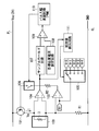
以上説明した技術的思想に基づく本発明の実施の形態のアクチュエータの駆動装置の構成について、図5に示すブロック図を用いて説明する。
<装置構成>
以上説明した技術的思想に基づく本発明の実施の形態のアクチュエータの駆動装置の構成について、図5に示すブロック図を用いて説明する。
図5において、電源電圧Vcc(例えば3V)を供給する電源ラインPLと接地ラインGLとの間に、電源ラインPL側から、PNPトランジスタ101(電流源トランジスタ)、SMAアクチュエータ3(抵抗値RSMA)および抵抗R1が直列に接続されている。SMAアクチュエータ3は、図1~図3に示したレンズ駆動装置100のSMAアクチュエータ3に相当する。
そして、SMAアクチュエータ3と抵抗R1との接続ノードはコンパレータ102の非反転入力(+)に接続され、コンパレータ102の出力は、抵抗R2およびスイッチ回路106を介して、PNPトランジスタ101のベースに接続されている。また、コンパレータ102の反転入力(-)には、基準電圧Vrが与えられる構成となっている。
SMAアクチュエータ3の、PNPトランジスタ101側の電位は、差動増幅器104の非反転入力(+)に与えられ、SMAアクチュエータ3の抵抗R1側の電位は、差動増幅器104の反転入力(-)に与えられる構成となっている。そして、差動増幅器104の出力は、サンプルホールド回路107および抵抗値検出回路111に与えられる構成となっている。
サンプルホールド回路107は、PWM制御におけるパルスがオンとなっている期間(オンパルス期間)、すなわち、定電流が供給されている期間に差動増幅器104で増幅されたSMAアクチュエータ3の両端の電位差、すなわち電圧をサンプリングし、当該電圧をPWM制御におけるパルスがオフとなっている期間も保持して出力する回路である。
サンプルホールド回路107から出力されるホールドされた電圧は、差動増幅器109の非反転入力(+)に与えられる。また、差動増幅器109の反転入力(-)には、目標位置電圧設定回路108から出力される目標位置電圧が与えられる構成となっており、差動増幅器109の出力は、パルス幅変調(PWM)回路110に与えられる。
パルス幅変調回路110は、差動増幅器109の出力に基づいてパルス幅変調したパルス信号を、スイッチ回路106に与え、パルス幅変調されたパルス信号に基づいてPNPトランジスタ101のオン、オフ制御を行う。
また、抵抗値検出回路111では、差動増幅器104の出力に基づいてSMAアクチュエータ3の抵抗値RSMAを検出し、検出した抵抗値に応じた基準電圧を基準電圧設定回路105により設定して、コンパレータ102の反転入力(-)に与える回路である。なお、図5に示す基準電圧設定回路105は、予め定めた複数の基準電圧(Vr0~Vr4)の中から基準電圧を選択する構成となっているが、これに限定されるものではなく、複数の基準電圧の段数に制限はなく、また、無段階で連続的に電圧を可変できる構成としても良い。
<装置動作>
以上説明したアクチュエータの駆動装置の動作について、図6に示すフローチャートを用いて説明する。
以上説明したアクチュエータの駆動装置の動作について、図6に示すフローチャートを用いて説明する。
レンズ駆動装置100を携帯電話機のカメラに使用するような場合、ステップS1においてカメラの電源を投入すると、直後に目標位置電圧設定回路108は、予め設定された当初の目標位置、あるいは、被写体にフォーカスするための目標位置を定め、目標位置に相当する電圧を設定して、目標位置電圧として出力する(ステップS2)。
一方、抵抗値検出回路111では、起動当初は、抵抗値測定用の基準電圧Vr0を選択して出力する(ステップS3)。この基準電圧Vr0は、定常動作時の基準電圧Vr1~Vr4より低く設定されており、起動当初には弱い電流をSMAアクチュエータ3に流すことにより、SMAアクチュエータ3が発熱して収縮するのを防ぎ、収縮していない状態での抵抗値RSMAを検出することができる。
すなわち、定電流回路は、基準電圧Vr0と抵抗R1とで決まる定電流をSMAアクチュエータ3に流し、差動増幅器104は、この時のSMAアクチュエータ3の両端の電圧を増幅して抵抗値検出回路111およびサンプルホールド回路107に出力する。
抵抗値検出回路111は、SMAアクチュエータ3の両端の電圧に基づいて抵抗値RSMAを検出し(ステップS4)、検出した抵抗値に応じた基準電圧を、基準電圧Vr1~Vr4の中から選択する(ステップS5)。以上が、電源投入時の初期動作である。ここで、基準電圧Vr1~Vr4は、電圧Va(図5)が電源電圧Vccに近い値となって、PNPトランジスタ101でのコレクタ損失を低減し、定電流回路での電力損失を最適化できるように抵抗値RSMAに合わせ予め準備されている。なお、基準電圧Vr1~Vr4は、抵抗値RSMAが比較的大きな場合は定電流値を小さくする値が選択され、抵抗値RSMAが比較的小さな場合は定電流値を大きくする値が選択されるように基準電圧設定回路105が制御される。
より具体的には、SMAアクチュエータ3の標準となる標準抵抗値(これをRSTと呼称)に応じた電圧を、基準電圧Vr1~Vr4の中から選択して標準電圧(これをVSTと呼称)とする。そして、検出された抵抗値RSMAがRSTよりも大きい場合には、RSTとRSMAとの差に応じて、VSTよりも小さい基準電圧を選択する。一方、検出された抵抗値RSMAがRSTよりも小さい場合には、RSTとRSMAとの差に応じて、VSTよりも大きい基準電圧を選択するように基準電圧設定回路105が制御される。
次に、定常動作時の駆動制御を説明する。定電流回路は、基準電圧Vrn(電源投入直後に検出された抵抗値に基づいて選択された基準電圧)と抵抗R1とで決まる定電流をSMAアクチュエータ3に流し(ステップS6)、差動増幅器104は、この時のSMAアクチュエータ3の両端の電圧を増幅して抵抗値検出回路111およびサンプルホールド回路107に出力する(ステップS7)。
サンプルホールド回路107は、定電流が供給されている期間の差動増幅器104の出力を保持し、その値を差動増幅器109に与え、差動増幅器109では目標位置電圧設定回路108から出力される目標位置電圧との比較を行って、その差を増幅して出力する(ステップS8)。
差動増幅器104の出力と目標位置電圧との差の電圧を受けたパルス幅変調回路110は、その差に基づいて、パルス幅変調されたパルス信号を生成してスイッチ回路106に与え、PNPトランジスタ101のオン、オフ制御を行う(ステップS9)。
ここで、電源投入当初は、当然、SMAアクチュエータ3は収縮しておらず、目標位置電圧よりもSMAアクチュエータ3の両端の電位差の方が高い。これは、SMAの電気特性によるものである。
このような場合、パルス幅変調されたパルス信号は、オン期間が長く設定され、SMAアクチュエータ3には、定電流が高い割合で流れることとなる。この電流により、SMAアクチュエータ3が発熱し、収縮を始める。SMAアクチュエータ3が収縮を始めると、レンズユニット1(図2)は目標位置に向かって移動を始める。
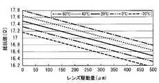
ここで、図7に、図1~3に示したレンズユニット1のオートフォーカス動作における駆動量に対する抵抗値の特性を示す。図7において、横軸にレンズの駆動量(μm)、縦軸に抵抗値(Ω)を示し、環境温度が60℃、40℃、20℃、0℃および-20℃の場合の特性を示している。
図7より、レンズ駆動量(収縮量)が大きくなると、抵抗値が下がり、また、環境温度が高くなると、抵抗値が高くなることが判る。このように、SMAの抵抗値は、収縮量と環境温度により変化する。
従って、SMAアクチュエータ3が収縮すると抵抗値が下がり、抵抗値が下がると、SMAアクチュエータ3の両端の電位差は小さくなり、目標位置電圧との差は小さくなる。これに従い、パルス幅変調されたパルス信号のオン期間が短くなり、目標位置電圧とSMAアクチュエータ3の両端の電位差とが等しくなった時点で、SMAの収縮は停止し、その収縮状態を維持する。この結果、レンズユニット1は目標位置付近で停止する。
この状態で目標位置電圧を変更するか否かを判定し(ステップS10)、目標位置電圧を変更しない場合はレンズ駆動を終了するが、目標位置電圧を変更する場合は、目標位置電圧設定回路108が、新たな目標位置電圧を設定し、ステップS7以下の動作を繰り返す。
目標位置電圧が変わると、差動増幅器109の出力が変化し、パルス幅変調されたパルス信号のオン期間も変わる。その変化の度合いにより、SMAアクチュエータ3はさらに収縮または、反対に膨張し、レンズユニット1が移動する。新しい目標位置電圧とSMA両端の電圧が等しくなったところで、SMAの収縮は停止し、その収縮状態を維持する。この結果、レンズユニット1は新しい目標位置付近で停止する。
なお、このように目標位置電圧を変更するのは、携帯電話用のカメラにおけるAF(オートフォーカス)シーケンスでは、無限位置から最近接位置までレンズを一定時間間隔で移動させるためであり、ステップS7以下の動作を繰り返すことで、AFシーケンスが実行される。
なお、このようなAFシーケンスにおける目標位置電圧は、無限位置相当の電圧から、最近接位置相当の電圧までを、予め定めたステップ数で分割した値となる。
<効果>
以上説明したように、本発明に係るアクチュエータの駆動装置においては、電源投入時の初期動作時に、予め定めた基準電圧Vr0をコンパレータ102に与え、基準電圧Vr0と抵抗R1とで決まる定電流をSMAアクチュエータ3に流し、この時のSMAアクチュエータ3の両端の電圧を検出する構成を採っている。
以上説明したように、本発明に係るアクチュエータの駆動装置においては、電源投入時の初期動作時に、予め定めた基準電圧Vr0をコンパレータ102に与え、基準電圧Vr0と抵抗R1とで決まる定電流をSMAアクチュエータ3に流し、この時のSMAアクチュエータ3の両端の電圧を検出する構成を採っている。
そして、検出した電圧に基づいて抵抗値検出回路111でSMAアクチュエータ3の抵抗値RSMAを検出し、検出した抵抗値に応じた基準電圧を設定して、コンパレータ102に与える構成を採っている。
このため、SMAアクチュエータ3の駆動初期の抵抗値に合わせた定電流値の変更が可能となる。この場合、設定する基準電圧は、SMAアクチュエータ3の端子電圧を、可能な限り電源電圧Vccに近づけることができるように、測定したSMAアクチュエータ3のRSMAに基づいて設定することで、PNPトランジスタ101での無効電力を低減して消費電力効率を向上させることができる。
ここで、SMAアクチュエータ3の抵抗値RSMAの変動要因は、1)SMA個々のばらつき、2)温度、3)経時変化および4)収縮の4要因が考えられる。
このうち、4)の収縮については、SMAアクチュエータ3を駆動した時に発生するものであるから、定電流値の調整、選択に際しては考慮しない。
先に説明したように、SMAアクチュエータ3の抵抗値RSMAは、1)、2)および3)の3つの要因により20%以上変動するが、そのうち1)に起因するものが約15%、2)に起因するものが約5%(-20℃~70℃の温度範囲)である。
従って、コンパレータ102に与える基準電圧を決定する際には、これらの変動要因を考慮し、抵抗値の変動に対応できるように、基準電圧のバリエーションを決定する。
なお、コンパレータ102に与える基準電圧については、図5に示したように、予め定めた複数の基準電圧の中から選択する構成でも良いが、無段階で連続的に変更する構成としても良い。この場合は、基準電圧の可変範囲の決定に際して、上述した変動要因を考慮する。
また、定電流源の定電流値を、SMAアクチュエータ3の抵抗値RSMAに基づいて最適化することは、PWM制御の制御能力の改善に繋がる。すなわち、SMAアクチュエータ3は、その特性上、同じ駆動量を得るのに、低温環境化ではより多くのパワーが必要となるが、PWM制御は、オンパルス幅を変えることにより、パワーを調整するので、低温ではオンパルス幅を広げる、すなわち、デューティー比を大きくする必要がある。この時のパワーの上限は、オンパルス幅が100%となる場合であるが、このようなパルスは現実的ではない。そこで、低温時に定電流値を増加させるように定電流値の最適化を行うことで、定電流値を固定している場合よりも、パワーの上限を大きくできる。
これは、高温時についても同様である。すなわち、SMAアクチュエータ3は、同じ駆動量を得るのに、高温環境化ではより少ないパワーで済むので、オンパルス幅は小さくする必要がある。しかし、オンパルス幅がある限度より小さくなると、動作が不安定になる等の不具合が発生する。そこで、高温時には定電流値を減少させるように定電流値の最適化を行うことで、定電流値を固定している場合よりも、オンパルス幅を広げることができ、上記不具合が解消される。
<変形例>
以上説明したアクチュエータの駆動装置においては、抵抗値検出回路111によりSMAアクチュエータ3の両端の電圧に基づいて抵抗値RSMAを検出して、検出した抵抗値RSMAに基づいて定常動作時の基準電圧を設定する構成であったが、抵抗値RSMAを検出するのではなく、アクチュエータの駆動装置の製造時に、抵抗値RSMAを検出し、そのデータを不揮発メモリ等の記憶装置(図示せず)に保持しておき、定常動作時には、当該記憶装置から抵抗値RSMAを読み出して、その値に基づいて基準電圧を設定する構成としても良い。
以上説明したアクチュエータの駆動装置においては、抵抗値検出回路111によりSMAアクチュエータ3の両端の電圧に基づいて抵抗値RSMAを検出して、検出した抵抗値RSMAに基づいて定常動作時の基準電圧を設定する構成であったが、抵抗値RSMAを検出するのではなく、アクチュエータの駆動装置の製造時に、抵抗値RSMAを検出し、そのデータを不揮発メモリ等の記憶装置(図示せず)に保持しておき、定常動作時には、当該記憶装置から抵抗値RSMAを読み出して、その値に基づいて基準電圧を設定する構成としても良い。
この場合、抵抗値検出回路111は、抵抗値検出の機能は不要となり、記憶装置から読み出した抵抗値RSMAに応じた基準電圧を、基準電圧Vr1~Vr4の中から選択する電流調整回路としての構成を有していれば良く、アクチュエータの駆動装置の構成を簡略化できる。
先に説明したように、抵抗値RSMAの変動要因の大部分は、SMA個々のばらつきが占めるので、製造時に検出した抵抗値RSMAのデータを用いることで、抵抗値RSMAの変動を考慮した基準電圧の設定が可能となる。
1 レンズユニット
2 レバー部材
2a 変位入力部
2b 変位出力部
3 形状記憶合金(SMA)アクチュエータ
4 ベース部材
6a,6b 平行板バネ
8 支持脚
8a レバー支持部
10 撮像レンズ
100 レンズ駆動装置
2 レバー部材
2a 変位入力部
2b 変位出力部
3 形状記憶合金(SMA)アクチュエータ
4 ベース部材
6a,6b 平行板バネ
8 支持脚
8a レバー支持部
10 撮像レンズ
100 レンズ駆動装置
Claims (7)
- 形状記憶合金ワイヤで構成され、該形状記憶合金ワイヤに電流を流すことで発生する熱に応じて前記形状記憶合金ワイヤが伸縮することに連動して、被駆動物を駆動するアクチュエータの駆動装置であって、
前記形状記憶合金ワイヤに定電流を供給する定電流回路と、
通電時の前記形状記憶合金ワイヤの抵抗値を検出し、検出した前記抵抗値に応じて前記定電流回路に流れる定電流値を調整する抵抗値検出回路と、
前記形状記憶合金ワイヤの両端の電位差に基づいて、パルス幅変調したパルス信号により前記定電流回路の電流源トランジスタのオン、オフ制御を行うパルス幅変調回路とを備え、
前記抵抗値検出回路は、
前記形状記憶合金ワイヤの前記抵抗値の大小に対する前記定電流値の大小の関係が反対となるように前記定電流値を調整する、アクチュエータの駆動装置。 - 前記定電流回路は、
前記電流源トランジスタに直列に接続された抵抗素子と、
前記抵抗素子に発生する電圧と基準電圧とが等しくなるように帰還制御を行うコンパレータとを備え、
前記形状記憶合金ワイヤは、前記抵抗素子と前記電流源トランジスタとの間に介挿され、
前記抵抗値検出回路は、
前記形状記憶合金ワイヤの前記抵抗値に基づいて、前記コンパレータに与える前記基準電圧の電圧値を変更することで、前記定電流回路の前記定電流値を調整する、請求項1記載のアクチュエータの駆動装置。 - 前記形状記憶合金ワイヤの前記抵抗値の検出は、初期動作として実行され、 前記抵抗値検出回路は、
前記形状記憶合金ワイヤの前記抵抗値の測定に際しては、前記被駆動物を駆動するための前記電圧値よりも小さい抵抗値測定用の電圧を前記基準電圧として前記コンパレータに与えることで、前記形状記憶合金ワイヤに通電して前記抵抗値を検出する、請求項2記載のアクチュエータの駆動装置。 - 前記抵抗値検出回路は、
前記形状記憶合金ワイヤの前記抵抗値の大小に対する前記定電流値の大小の関係が反対となるように前記基準電圧の前記電圧値を変更する、請求項2記載のアクチュエータの駆動装置。 - 形状記憶合金ワイヤで構成され、該形状記憶合金ワイヤに電流を流すことで発生する熱に応じて前記形状記憶合金ワイヤが伸縮することに連動して、被駆動物を駆動するアクチュエータの駆動装置であって、
前記形状記憶合金ワイヤに定電流を供給する定電流回路と、
通電時の前記形状記憶合金ワイヤの抵抗値に関するデータを保持する記憶部と、
前記記憶部に保持された前記抵抗値に応じて前記定電流回路に流れる定電流値を調整する電流調整回路と、
前記形状記憶合金ワイヤの両端の電位差に基づいて、パルス幅変調したパルス信号により前記定電流回路の電流源トランジスタのオン、オフ制御を行うパルス幅変調回路とを備え、
前記電流調整回路は、
前記定電流回路の電力消費を低減するように前記定電流値を調整する、アクチュエータの駆動装置。 - 形状記憶合金ワイヤに定電流回路から電流を流すことで前記形状記憶合金ワイヤを伸縮させて被駆動物を駆動するアクチュエータの駆動方法であって、
(a)通電時の前記形状記憶合金ワイヤの抵抗値を検出するステップと、
(b)検出された前記抵抗値に応じて前記定電流回路に流れる定電流値を調整するステップと、
(c)前記形状記憶合金ワイヤの両端の電位差に基づいて、前記形状記憶合金ワイヤに供給される電流をパルス幅変調するステップと、を有し、
前記ステップ(b)は、
前記形状記憶合金ワイヤの前記抵抗値の大小に対する前記定電流値の大小の関係が反対となるように前記定電流値を調整するステップを含む、アクチュエータの駆動方法。 - 前記ステップ(a)は、
前記形状記憶合金ワイヤが収縮しない電流を前記形状記憶合金ワイヤに通電するステップを含む、請求項6記載のアクチュエータの駆動方法。
Applications Claiming Priority (2)
| Application Number | Priority Date | Filing Date | Title |
|---|---|---|---|
| JP2010-113932 | 2010-05-18 | ||
| JP2010113932 | 2010-05-18 |
Publications (1)
| Publication Number | Publication Date |
|---|---|
| WO2011145463A1 true WO2011145463A1 (ja) | 2011-11-24 |
Family
ID=44991574
Family Applications (1)
| Application Number | Title | Priority Date | Filing Date |
|---|---|---|---|
| PCT/JP2011/060634 Ceased WO2011145463A1 (ja) | 2010-05-18 | 2011-05-09 | アクチュエータの駆動装置および駆動方法 |
Country Status (1)
| Country | Link |
|---|---|
| WO (1) | WO2011145463A1 (ja) |
Cited By (4)
| Publication number | Priority date | Publication date | Assignee | Title |
|---|---|---|---|---|
| CN106170626A (zh) * | 2014-12-25 | 2016-11-30 | Smk株式会社 | 冲击产生致动器、触摸面板及驱动方法 |
| JP2017210909A (ja) * | 2016-05-25 | 2017-11-30 | レノボ・シンガポール・プライベート・リミテッド | 形状記憶合金を利用したアクチュエータの駆動システム、電子機器、パルス幅の決定方法および触覚フィードバックの調整方法 |
| CN111918002A (zh) * | 2019-05-10 | 2020-11-10 | 华为技术有限公司 | 一种摄像装置中形状记忆合金马达的控制方法和摄像装置 |
| CN113873170A (zh) * | 2021-10-29 | 2021-12-31 | 上海艾为电子技术股份有限公司 | 光学防抖控制系统、方法及电子设备 |
Citations (7)
| Publication number | Priority date | Publication date | Assignee | Title |
|---|---|---|---|---|
| JPH06131612A (ja) * | 1992-10-14 | 1994-05-13 | Matsushita Electric Ind Co Ltd | 磁気再生装置 |
| JP2006183564A (ja) * | 2004-12-27 | 2006-07-13 | Toki Corporation Kk | アクチュエータ |
| JP2008238641A (ja) * | 2007-03-28 | 2008-10-09 | Seiko Epson Corp | 駆動信号生成装置、液体吐出装置、及び、駆動信号生成方法 |
| JP2008274898A (ja) * | 2007-05-07 | 2008-11-13 | Konica Minolta Opto Inc | 駆動ユニットおよび可動モジュール |
| JP2009013891A (ja) * | 2007-07-05 | 2009-01-22 | Konica Minolta Opto Inc | 形状記憶合金の駆動装置およびそれを用いる撮像装置 |
| JP2009127578A (ja) * | 2007-11-27 | 2009-06-11 | Seiko Instruments Inc | 形状記憶合金アクチュエータおよびそれを備える電子機器 |
| WO2009071898A2 (en) * | 2007-12-03 | 2009-06-11 | Cambridge Mechatronics Limited | Control of a shape memory alloy actuation arrangement |
-
2011
- 2011-05-09 WO PCT/JP2011/060634 patent/WO2011145463A1/ja not_active Ceased
Patent Citations (7)
| Publication number | Priority date | Publication date | Assignee | Title |
|---|---|---|---|---|
| JPH06131612A (ja) * | 1992-10-14 | 1994-05-13 | Matsushita Electric Ind Co Ltd | 磁気再生装置 |
| JP2006183564A (ja) * | 2004-12-27 | 2006-07-13 | Toki Corporation Kk | アクチュエータ |
| JP2008238641A (ja) * | 2007-03-28 | 2008-10-09 | Seiko Epson Corp | 駆動信号生成装置、液体吐出装置、及び、駆動信号生成方法 |
| JP2008274898A (ja) * | 2007-05-07 | 2008-11-13 | Konica Minolta Opto Inc | 駆動ユニットおよび可動モジュール |
| JP2009013891A (ja) * | 2007-07-05 | 2009-01-22 | Konica Minolta Opto Inc | 形状記憶合金の駆動装置およびそれを用いる撮像装置 |
| JP2009127578A (ja) * | 2007-11-27 | 2009-06-11 | Seiko Instruments Inc | 形状記憶合金アクチュエータおよびそれを備える電子機器 |
| WO2009071898A2 (en) * | 2007-12-03 | 2009-06-11 | Cambridge Mechatronics Limited | Control of a shape memory alloy actuation arrangement |
Cited By (7)
| Publication number | Priority date | Publication date | Assignee | Title |
|---|---|---|---|---|
| CN106170626A (zh) * | 2014-12-25 | 2016-11-30 | Smk株式会社 | 冲击产生致动器、触摸面板及驱动方法 |
| JP2017210909A (ja) * | 2016-05-25 | 2017-11-30 | レノボ・シンガポール・プライベート・リミテッド | 形状記憶合金を利用したアクチュエータの駆動システム、電子機器、パルス幅の決定方法および触覚フィードバックの調整方法 |
| CN111918002A (zh) * | 2019-05-10 | 2020-11-10 | 华为技术有限公司 | 一种摄像装置中形状记忆合金马达的控制方法和摄像装置 |
| CN111918002B (zh) * | 2019-05-10 | 2022-02-18 | 华为技术有限公司 | 一种摄像装置中形状记忆合金马达的控制方法和摄像装置 |
| US12321035B2 (en) | 2019-05-10 | 2025-06-03 | Huawei Technologies Co., Ltd. | Control method for shape memory alloy motor in photographing apparatus and photographing apparatus |
| CN113873170A (zh) * | 2021-10-29 | 2021-12-31 | 上海艾为电子技术股份有限公司 | 光学防抖控制系统、方法及电子设备 |
| CN113873170B (zh) * | 2021-10-29 | 2023-09-01 | 上海艾为电子技术股份有限公司 | 光学防抖控制系统、方法及电子设备 |
Similar Documents
| Publication | Publication Date | Title |
|---|---|---|
| US8189093B2 (en) | Drive unit and drive module | |
| JP4946675B2 (ja) | 形状記憶合金の駆動装置およびそれを用いる撮像装置ならびに形状記憶合金の駆動方法 | |
| CN101668947B (zh) | 形状记忆合金驱动设备 | |
| US8446475B2 (en) | Shape memory alloy actuation apparatus | |
| CN108292074B (zh) | 对sma致动装置的控制 | |
| JP5548211B2 (ja) | 形状記憶合金アクチュエータ装置の制御 | |
| US8174608B2 (en) | Drive unit and drive module | |
| US8395855B2 (en) | Shape memory alloy actuation apparatus | |
| JP4853011B2 (ja) | 駆動装置の製造システム、及び駆動装置の製造方法 | |
| JP5126362B2 (ja) | レンズ駆動装置 | |
| WO2008129290A1 (en) | Control circuits for an sma actuator | |
| JP2009037059A (ja) | 駆動機構、駆動装置およびレンズ駆動装置 | |
| GB2491684A (en) | Using resistance to determine ambient temperature of SMA actuator | |
| WO2009090960A1 (ja) | 形状記憶合金駆動装置 | |
| WO2011145463A1 (ja) | アクチュエータの駆動装置および駆動方法 | |
| US20130003201A1 (en) | Driving Mechanism, Driving Device, and Method of Manufacturing Driving Device | |
| WO2012005072A1 (ja) | 形状記憶合金アクチュエータ制御装置および光学部品駆動ユニット | |
| JP2012159046A (ja) | アクチュエータの駆動装置およびレンズ駆動装置 | |
| JP4966265B2 (ja) | 電流ドライバ回路 | |
| JP2012227998A (ja) | 製造方法、および製造装置 | |
| WO2012093567A1 (ja) | 形状記憶合金アクチュエータ制御装置および光学部品駆動ユニット | |
| JP2010072415A (ja) | 駆動機構、駆動装置 | |
| JP2007278797A (ja) | 位置検出装置、レンズ鏡筒、カメラおよび位置検出回路の調節方法 | |
| JP2012078418A (ja) | オートフォーカス装置、該オートフォーカス装置を搭載した撮像装置、及び、該撮像装置を搭載した携帯電子機器 |
Legal Events
| Date | Code | Title | Description |
|---|---|---|---|
| 121 | Ep: the epo has been informed by wipo that ep was designated in this application |
Ref document number: 11783400 Country of ref document: EP Kind code of ref document: A1 |
|
| NENP | Non-entry into the national phase |
Ref country code: DE |
|
| 122 | Ep: pct application non-entry in european phase |
Ref document number: 11783400 Country of ref document: EP Kind code of ref document: A1 |
|
| NENP | Non-entry into the national phase |
Ref country code: JP |