WO2011129441A1 - Dispositif à semiconducteur - Google Patents
Dispositif à semiconducteur Download PDFInfo
- Publication number
- WO2011129441A1 WO2011129441A1 PCT/JP2011/059410 JP2011059410W WO2011129441A1 WO 2011129441 A1 WO2011129441 A1 WO 2011129441A1 JP 2011059410 W JP2011059410 W JP 2011059410W WO 2011129441 A1 WO2011129441 A1 WO 2011129441A1
- Authority
- WO
- WIPO (PCT)
- Prior art keywords
- thin film
- film transistor
- region
- tft
- semiconductor device
- Prior art date
Links
- 239000004065 semiconductor Substances 0.000 title claims abstract description 186
- 239000010409 thin film Substances 0.000 claims abstract description 126
- 239000010408 film Substances 0.000 claims abstract description 109
- 230000003287 optical effect Effects 0.000 claims abstract description 104
- 239000000758 substrate Substances 0.000 claims abstract description 48
- 239000003990 capacitor Substances 0.000 claims abstract description 38
- 239000012535 impurity Substances 0.000 claims description 77
- 239000010410 layer Substances 0.000 description 173
- 238000000034 method Methods 0.000 description 26
- ZOXJGFHDIHLPTG-UHFFFAOYSA-N Boron Chemical compound [B] ZOXJGFHDIHLPTG-UHFFFAOYSA-N 0.000 description 23
- 229910052796 boron Inorganic materials 0.000 description 23
- 150000002500 ions Chemical class 0.000 description 22
- 239000004973 liquid crystal related substance Substances 0.000 description 20
- 238000002513 implantation Methods 0.000 description 15
- 230000003197 catalytic effect Effects 0.000 description 14
- 238000005468 ion implantation Methods 0.000 description 13
- PXHVJJICTQNCMI-UHFFFAOYSA-N Nickel Chemical compound [Ni] PXHVJJICTQNCMI-UHFFFAOYSA-N 0.000 description 11
- 239000011159 matrix material Substances 0.000 description 11
- 230000007423 decrease Effects 0.000 description 10
- 238000004519 manufacturing process Methods 0.000 description 10
- 229910021417 amorphous silicon Inorganic materials 0.000 description 9
- 239000013078 crystal Substances 0.000 description 9
- VYPSYNLAJGMNEJ-UHFFFAOYSA-N Silicium dioxide Chemical compound O=[Si]=O VYPSYNLAJGMNEJ-UHFFFAOYSA-N 0.000 description 8
- 239000011229 interlayer Substances 0.000 description 8
- 229910052814 silicon oxide Inorganic materials 0.000 description 8
- 238000002425 crystallisation Methods 0.000 description 7
- 238000010586 diagram Methods 0.000 description 6
- 230000035945 sensitivity Effects 0.000 description 6
- OAICVXFJPJFONN-UHFFFAOYSA-N Phosphorus Chemical compound [P] OAICVXFJPJFONN-UHFFFAOYSA-N 0.000 description 5
- 229910021419 crystalline silicon Inorganic materials 0.000 description 5
- 230000008025 crystallization Effects 0.000 description 5
- 238000010438 heat treatment Methods 0.000 description 5
- 229910052751 metal Inorganic materials 0.000 description 5
- 239000002184 metal Substances 0.000 description 5
- 229910052759 nickel Inorganic materials 0.000 description 5
- 229910052698 phosphorus Inorganic materials 0.000 description 5
- 239000011574 phosphorus Substances 0.000 description 5
- 238000004544 sputter deposition Methods 0.000 description 5
- 229910052581 Si3N4 Inorganic materials 0.000 description 4
- 238000009792 diffusion process Methods 0.000 description 4
- PCHJSUWPFVWCPO-UHFFFAOYSA-N gold Chemical compound [Au] PCHJSUWPFVWCPO-UHFFFAOYSA-N 0.000 description 4
- 238000005268 plasma chemical vapour deposition Methods 0.000 description 4
- HQVNEWCFYHHQES-UHFFFAOYSA-N silicon nitride Chemical compound N12[Si]34N5[Si]62N3[Si]51N64 HQVNEWCFYHHQES-UHFFFAOYSA-N 0.000 description 4
- 239000002356 single layer Substances 0.000 description 4
- KDLHZDBZIXYQEI-UHFFFAOYSA-N Palladium Chemical compound [Pd] KDLHZDBZIXYQEI-UHFFFAOYSA-N 0.000 description 3
- 239000003054 catalyst Substances 0.000 description 3
- 238000005229 chemical vapour deposition Methods 0.000 description 3
- 238000005224 laser annealing Methods 0.000 description 3
- 229910052750 molybdenum Inorganic materials 0.000 description 3
- BASFCYQUMIYNBI-UHFFFAOYSA-N platinum Chemical compound [Pt] BASFCYQUMIYNBI-UHFFFAOYSA-N 0.000 description 3
- 230000001681 protective effect Effects 0.000 description 3
- 238000003860 storage Methods 0.000 description 3
- 229910052715 tantalum Inorganic materials 0.000 description 3
- 229910052719 titanium Inorganic materials 0.000 description 3
- 229910052721 tungsten Inorganic materials 0.000 description 3
- 239000007864 aqueous solution Substances 0.000 description 2
- 229910052785 arsenic Inorganic materials 0.000 description 2
- RQNWIZPPADIBDY-UHFFFAOYSA-N arsenic atom Chemical compound [As] RQNWIZPPADIBDY-UHFFFAOYSA-N 0.000 description 2
- 239000000969 carrier Substances 0.000 description 2
- 150000001875 compounds Chemical class 0.000 description 2
- 239000010949 copper Substances 0.000 description 2
- 238000000151 deposition Methods 0.000 description 2
- 238000001514 detection method Methods 0.000 description 2
- 230000000694 effects Effects 0.000 description 2
- 230000005684 electric field Effects 0.000 description 2
- 239000007789 gas Substances 0.000 description 2
- 239000010931 gold Substances 0.000 description 2
- 229910052738 indium Inorganic materials 0.000 description 2
- APFVFJFRJDLVQX-UHFFFAOYSA-N indium atom Chemical compound [In] APFVFJFRJDLVQX-UHFFFAOYSA-N 0.000 description 2
- 238000002347 injection Methods 0.000 description 2
- 239000007924 injection Substances 0.000 description 2
- 238000005499 laser crystallization Methods 0.000 description 2
- 239000000463 material Substances 0.000 description 2
- 238000000059 patterning Methods 0.000 description 2
- 238000000206 photolithography Methods 0.000 description 2
- 238000004151 rapid thermal annealing Methods 0.000 description 2
- 239000010948 rhodium Substances 0.000 description 2
- 238000001771 vacuum deposition Methods 0.000 description 2
- RYGMFSIKBFXOCR-UHFFFAOYSA-N Copper Chemical compound [Cu] RYGMFSIKBFXOCR-UHFFFAOYSA-N 0.000 description 1
- XEEYBQQBJWHFJM-UHFFFAOYSA-N Iron Chemical compound [Fe] XEEYBQQBJWHFJM-UHFFFAOYSA-N 0.000 description 1
- KJTLSVCANCCWHF-UHFFFAOYSA-N Ruthenium Chemical compound [Ru] KJTLSVCANCCWHF-UHFFFAOYSA-N 0.000 description 1
- XUIMIQQOPSSXEZ-UHFFFAOYSA-N Silicon Chemical compound [Si] XUIMIQQOPSSXEZ-UHFFFAOYSA-N 0.000 description 1
- ATJFFYVFTNAWJD-UHFFFAOYSA-N Tin Chemical compound [Sn] ATJFFYVFTNAWJD-UHFFFAOYSA-N 0.000 description 1
- MQRWBMAEBQOWAF-UHFFFAOYSA-N acetic acid;nickel Chemical compound [Ni].CC(O)=O.CC(O)=O MQRWBMAEBQOWAF-UHFFFAOYSA-N 0.000 description 1
- 230000003213 activating effect Effects 0.000 description 1
- 229910052782 aluminium Inorganic materials 0.000 description 1
- 229910021486 amorphous silicon dioxide Inorganic materials 0.000 description 1
- 230000003321 amplification Effects 0.000 description 1
- 238000000137 annealing Methods 0.000 description 1
- 239000012298 atmosphere Substances 0.000 description 1
- 230000000903 blocking effect Effects 0.000 description 1
- 229910017052 cobalt Inorganic materials 0.000 description 1
- 239000010941 cobalt Substances 0.000 description 1
- GUTLYIVDDKVIGB-UHFFFAOYSA-N cobalt atom Chemical compound [Co] GUTLYIVDDKVIGB-UHFFFAOYSA-N 0.000 description 1
- 239000004020 conductor Substances 0.000 description 1
- 229910052802 copper Inorganic materials 0.000 description 1
- 230000003247 decreasing effect Effects 0.000 description 1
- 230000006866 deterioration Effects 0.000 description 1
- 238000005530 etching Methods 0.000 description 1
- 239000011521 glass Substances 0.000 description 1
- 229910052737 gold Inorganic materials 0.000 description 1
- 238000005984 hydrogenation reaction Methods 0.000 description 1
- 239000012212 insulator Substances 0.000 description 1
- 229910052741 iridium Inorganic materials 0.000 description 1
- GKOZUEZYRPOHIO-UHFFFAOYSA-N iridium atom Chemical compound [Ir] GKOZUEZYRPOHIO-UHFFFAOYSA-N 0.000 description 1
- 230000001678 irradiating effect Effects 0.000 description 1
- 238000002955 isolation Methods 0.000 description 1
- 238000005259 measurement Methods 0.000 description 1
- 229940078494 nickel acetate Drugs 0.000 description 1
- RUFLMLWJRZAWLJ-UHFFFAOYSA-N nickel silicide Chemical compound [Ni]=[Si]=[Ni] RUFLMLWJRZAWLJ-UHFFFAOYSA-N 0.000 description 1
- 229910021334 nickel silicide Inorganic materials 0.000 description 1
- 239000012299 nitrogen atmosphere Substances 0.000 description 1
- 238000003199 nucleic acid amplification method Methods 0.000 description 1
- 229910052762 osmium Inorganic materials 0.000 description 1
- SYQBFIAQOQZEGI-UHFFFAOYSA-N osmium atom Chemical compound [Os] SYQBFIAQOQZEGI-UHFFFAOYSA-N 0.000 description 1
- 229910052763 palladium Inorganic materials 0.000 description 1
- 229910052697 platinum Inorganic materials 0.000 description 1
- 230000001737 promoting effect Effects 0.000 description 1
- 239000011347 resin Substances 0.000 description 1
- 229920005989 resin Polymers 0.000 description 1
- 229910052703 rhodium Inorganic materials 0.000 description 1
- MHOVAHRLVXNVSD-UHFFFAOYSA-N rhodium atom Chemical compound [Rh] MHOVAHRLVXNVSD-UHFFFAOYSA-N 0.000 description 1
- 230000000630 rising effect Effects 0.000 description 1
- 229910052707 ruthenium Inorganic materials 0.000 description 1
- 229910052710 silicon Inorganic materials 0.000 description 1
- 239000010703 silicon Substances 0.000 description 1
- 238000004528 spin coating Methods 0.000 description 1
- 238000007740 vapor deposition Methods 0.000 description 1
Images


Classifications
-
- H—ELECTRICITY
- H01—ELECTRIC ELEMENTS
- H01L—SEMICONDUCTOR DEVICES NOT COVERED BY CLASS H10
- H01L27/00—Devices consisting of a plurality of semiconductor or other solid-state components formed in or on a common substrate
- H01L27/14—Devices consisting of a plurality of semiconductor or other solid-state components formed in or on a common substrate including semiconductor components sensitive to infrared radiation, light, electromagnetic radiation of shorter wavelength or corpuscular radiation and specially adapted either for the conversion of the energy of such radiation into electrical energy or for the control of electrical energy by such radiation
- H01L27/144—Devices controlled by radiation
- H01L27/146—Imager structures
- H01L27/14678—Contact-type imagers
-
- G—PHYSICS
- G02—OPTICS
- G02F—OPTICAL DEVICES OR ARRANGEMENTS FOR THE CONTROL OF LIGHT BY MODIFICATION OF THE OPTICAL PROPERTIES OF THE MEDIA OF THE ELEMENTS INVOLVED THEREIN; NON-LINEAR OPTICS; FREQUENCY-CHANGING OF LIGHT; OPTICAL LOGIC ELEMENTS; OPTICAL ANALOGUE/DIGITAL CONVERTERS
- G02F1/00—Devices or arrangements for the control of the intensity, colour, phase, polarisation or direction of light arriving from an independent light source, e.g. switching, gating or modulating; Non-linear optics
- G02F1/01—Devices or arrangements for the control of the intensity, colour, phase, polarisation or direction of light arriving from an independent light source, e.g. switching, gating or modulating; Non-linear optics for the control of the intensity, phase, polarisation or colour
- G02F1/13—Devices or arrangements for the control of the intensity, colour, phase, polarisation or direction of light arriving from an independent light source, e.g. switching, gating or modulating; Non-linear optics for the control of the intensity, phase, polarisation or colour based on liquid crystals, e.g. single liquid crystal display cells
- G02F1/133—Constructional arrangements; Operation of liquid crystal cells; Circuit arrangements
- G02F1/136—Liquid crystal cells structurally associated with a semi-conducting layer or substrate, e.g. cells forming part of an integrated circuit
- G02F1/1362—Active matrix addressed cells
- G02F1/1368—Active matrix addressed cells in which the switching element is a three-electrode device
-
- G—PHYSICS
- G06—COMPUTING; CALCULATING OR COUNTING
- G06F—ELECTRIC DIGITAL DATA PROCESSING
- G06F3/00—Input arrangements for transferring data to be processed into a form capable of being handled by the computer; Output arrangements for transferring data from processing unit to output unit, e.g. interface arrangements
- G06F3/01—Input arrangements or combined input and output arrangements for interaction between user and computer
- G06F3/03—Arrangements for converting the position or the displacement of a member into a coded form
- G06F3/041—Digitisers, e.g. for touch screens or touch pads, characterised by the transducing means
- G06F3/042—Digitisers, e.g. for touch screens or touch pads, characterised by the transducing means by opto-electronic means
-
- H—ELECTRICITY
- H01—ELECTRIC ELEMENTS
- H01L—SEMICONDUCTOR DEVICES NOT COVERED BY CLASS H10
- H01L27/00—Devices consisting of a plurality of semiconductor or other solid-state components formed in or on a common substrate
- H01L27/14—Devices consisting of a plurality of semiconductor or other solid-state components formed in or on a common substrate including semiconductor components sensitive to infrared radiation, light, electromagnetic radiation of shorter wavelength or corpuscular radiation and specially adapted either for the conversion of the energy of such radiation into electrical energy or for the control of electrical energy by such radiation
- H01L27/144—Devices controlled by radiation
- H01L27/146—Imager structures
- H01L27/14643—Photodiode arrays; MOS imagers
- H01L27/14645—Colour imagers
-
- G—PHYSICS
- G02—OPTICS
- G02F—OPTICAL DEVICES OR ARRANGEMENTS FOR THE CONTROL OF LIGHT BY MODIFICATION OF THE OPTICAL PROPERTIES OF THE MEDIA OF THE ELEMENTS INVOLVED THEREIN; NON-LINEAR OPTICS; FREQUENCY-CHANGING OF LIGHT; OPTICAL LOGIC ELEMENTS; OPTICAL ANALOGUE/DIGITAL CONVERTERS
- G02F1/00—Devices or arrangements for the control of the intensity, colour, phase, polarisation or direction of light arriving from an independent light source, e.g. switching, gating or modulating; Non-linear optics
- G02F1/01—Devices or arrangements for the control of the intensity, colour, phase, polarisation or direction of light arriving from an independent light source, e.g. switching, gating or modulating; Non-linear optics for the control of the intensity, phase, polarisation or colour
- G02F1/13—Devices or arrangements for the control of the intensity, colour, phase, polarisation or direction of light arriving from an independent light source, e.g. switching, gating or modulating; Non-linear optics for the control of the intensity, phase, polarisation or colour based on liquid crystals, e.g. single liquid crystal display cells
- G02F1/133—Constructional arrangements; Operation of liquid crystal cells; Circuit arrangements
- G02F1/1333—Constructional arrangements; Manufacturing methods
- G02F1/13338—Input devices, e.g. touch panels
Definitions
- the present invention relates to a semiconductor device including an optical sensor unit including a thin film diode (TFD).
- an optical sensor unit including a thin film diode (TFD).
- TFD thin film diode
- Patent Document 1 proposes forming a semiconductor layer of a TFD and a thin film transistor (TFT) having different crystal states from the same amorphous semiconductor film. These TFD and TFT can be applied to a display device including an optical touch panel, for example.
- TFD and TFT thin film transistor
- a TFT is provided for each pixel in the display area and is used as a pixel switching element (pixel TFT). Further, it is provided in a frame area arranged around the display area, and is used as a driving circuit TFT constituting a driving circuit.
- the TFD is used as a light receiving element. For example, by providing an optical sensor unit including TFD in the display area, an object such as a finger in contact with the screen can be detected using external light.
- Patent Document 2 proposes to perform sensing using invisible light emitted from a backlight using a sensor that detects invisible light in a display device including an optical touch panel.
- a sensor that detects invisible light in a display device including an optical touch panel.
- an invisible light beam that is emitted from a backlight and reflected by an object such as a finger that is in contact with the screen is detected by a sensor provided in each pixel of the display device.
- FIG. 11 is a circuit diagram showing a configuration of the optical sensor unit disclosed in Patent Document 1.
- the optical sensor unit includes an optical sensor thin film diode (hereinafter “optical sensor TFD”) 701, a signal storage capacitor 702, and a thin film transistor (hereinafter referred to as “buffer”) for amplifying and extracting a signal stored in the capacitor 702. TFT ”) 703.
- optical sensor TFD optical sensor thin film diode
- buffer thin film transistor
- the photocurrent generated by the optical sensor TFD is accumulated in a capacitor (condenser) and held for a certain period.
- a capacitor condenser
- the present applicant refers to a switching transistor (hereinafter referred to as “holding TFT”) between a photosensor thin film diode and a capacitor in order to control the holding and reading of the photocurrent. .) Is proposed. When the holding TFT is in the OFF state, the photocurrent is held in the capacitor, and when the holding TFT is in the ON state, the accumulated photocurrent is collectively read.
- these TFT and TFD are preferably formed by a common process using the same semiconductor film.
- the electrical characteristics required for these TFTs are different from each other. Specifically, since the driving circuit TFT needs to operate at high speed, the driving circuit TFT is required to have a large current driving capability, that is, a large on-current. On the other hand, the pixel TFT and the holding TFT are required to have a small off-leakage current. In the liquid crystal display device, it is necessary to hold the voltage applied to the liquid crystal during the period of one frame until the screen is rewritten. This is because when the off-current (off-leakage current) of the pixel TFT is large, the voltage applied to the liquid crystal may be reduced with time to deteriorate display characteristics.
- the off-leakage current of the holding TFT in the holding period in which the holding TFT is turned off and the photocurrent is held in the capacitor Is required to be small.
- the holding TFT needs to hold a minute charge generated in the TFD, a low leakage characteristic superior to that of the pixel TFT is required.
- the specification that the off-leakage current Ioff is less than 2 pA temperature: measured value in white light 10000 lx up to 60 ° C.
- the off-leakage current Ioff may be less than 13 pA. Further, the off-leakage current Ioff may increase from 13 pA due to the light leakage current.
- the pixel TFT and the holding TFT are common in that it is preferable that the off-leakage current is small.
- suitable ranges of on-current and off-leakage current differ from one another depending on the application of each TFT.
- the present invention has been made in view of the above circumstances, and an object of the present invention is to provide a thin film transistor for a pixel and a thin film transistor used in the optical sensor unit in a semiconductor device including the optical sensor unit using a thin film diode.
- the characteristic is to be controlled according to the characteristic required for each thin film transistor.
- the semiconductor device of the present invention is a semiconductor device including a display region having a plurality of pixels, the substrate, a first conductivity type first thin film transistor formed for each pixel on the substrate, and the display.
- a plurality of photosensor units that are formed on the substrate and that detect light and generate sensing signals, each of the photosensor units including a light receiving unit including at least one thin film diode;
- An ion has a semiconductor layer formed from the same semiconductor film, and the semiconductor layers of the first and second thin film transistors are both a source and drain region and a channel region located between these regions. The characteristics of the first thin film transistor and the characteristics of the second thin film transistor are different.
- the threshold voltage of the first thin film transistor is different from the threshold voltage of the second thin film transistor.
- each of the channel regions of the first and second thin film transistors contains an impurity of a second conductivity type different from the first conductivity type, and the first and second thin film transistors The concentration of the second conductivity type impurity in the channel region is different from each other.
- the off-leak current of the first thin film transistor is different from the off-leak current of the second thin film transistor.
- the off-leak current of the second thin film transistor may be smaller than the off-leak current of the first thin film transistor.
- the second thin film transistor is formed between the source and drain regions and the channel region, and includes a low-concentration impurity containing a first conductivity type impurity at a lower concentration than the source and drain regions.
- the low concentration impurity region does not overlap with the gate electrode.
- the first thin film transistor has a low-concentration impurity region formed between the source and drain regions and the channel region, and containing a first conductivity type impurity at a lower concentration than the source and drain regions.
- the low-concentration impurity region does not overlap with the gate electrode, and the concentration of the first conductivity type impurity in the low-concentration impurity region of the first and second thin film transistors may be different from each other.
- the second thin film transistor may have a multi-gate structure.
- the second thin film transistor may have a triple gate structure.
- a light shielding layer is formed between the semiconductor layer of the second thin film transistor and the substrate so as to overlap at least the channel region of the semiconductor layer of the second thin film transistor.
- the potential of the light shielding layer may be fixed.
- a sensor light-shielding layer may be disposed between the semiconductor layer of the at least one thin film diode and the substrate, and the sensor light-shielding layer and the light-shielding layer may be electrically connected.
- the semiconductor layer of the thin film diode has a p-type region, an n-type region, and an intrinsic region located between the p-type region and the n-type region.
- the first conductivity type may be n-type, and the second conductivity type may be p-type.
- the display device further includes another thin film transistor formed on the substrate in a region other than the display region, wherein the other thin film transistor is formed of the same semiconductor film, and includes a source and drain region and a channel region. The characteristics of the other thin film transistor are different from those of the second thin film transistor.
- the concentration of the second conductivity type impurity in the channel region of the other thin film transistor and the second thin film transistor is different from each other.
- the apparatus further includes a backlight that emits visible light and infrared light, and the thin-film diode can detect the infrared light.
- the optical sensor unit may be arranged corresponding to each pixel or a set of two or more pixels.
- Another semiconductor device of the present invention includes a substrate, a plurality of first conductive type first thin film transistors formed on the substrate, and a plurality of sensing signals generated by detecting light.
- the first and second thin film transistors and the at least one thin film diode have a semiconductor layer formed of the same semiconductor film, and the first and second thin film transistors
- the semiconductor layer of the thin film transistor, both the source and drain regions, and a channel region located between these regions is different from the characteristic of the said characteristic of the first thin film transistor second thin film transistor.
- the characteristics of the thin film transistor for the pixel and the thin film transistor used in the optical sensor unit are in accordance with the characteristics required for each thin film transistor. Can be controlled.
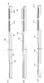
- FIG. 6C is a cross-sectional view of the pixel TFT, the holding TFT, and the optical sensor TFD. It is typical sectional drawing which shows an example of the display apparatus using the semiconductor device of 1st Embodiment by this invention. It is a graph which shows the relationship between the electric potential Vls of the light shielding layer of holding TFT, and ON current Ion at the time of changing the boron injection amount to a channel area
- FIGS. 7A to 7C are schematic cross-sectional views illustrating manufacturing steps of a semiconductor device according to a second embodiment of the present invention.
- FIGS. (D) to (F) are schematic cross-sectional views illustrating the manufacturing steps of the semiconductor device of the second embodiment according to the present invention.
- (G) to (I) are schematic cross-sectional views showing manufacturing steps of the semiconductor device according to the second embodiment of the present invention. It is a figure which shows the structure of the other active matrix substrate of embodiment by this invention.
- FIG. 1 It is a top view which shows the structure of the other active matrix substrate of embodiment by this invention. It is a circuit diagram which shows the structure of the conventional optical sensor part.
- (A)-(c) is a schematic diagram for demonstrating an example of the system which performs sensing only using backlight light. It is a figure which illustrates the operation timing of the sensor in the sensing system shown in FIG.
- the semiconductor device of the present embodiment is an active matrix substrate provided with an optical sensor unit.
- the active matrix substrate of this embodiment can be widely applied to display devices such as liquid crystal display devices and organic EL display devices. In particular, it is suitably used for a liquid crystal display device having a touch panel function.
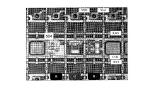
- FIG. 1A is a schematic plan view showing an example of the semiconductor device 100 of the present embodiment
- FIG. 1B is a circuit diagram showing the configuration of the optical sensor unit 200 in the semiconductor device 100
- FIG. 1C is a schematic cross-sectional view illustrating an example of a pixel TFT, a holding TFT, and an optical sensor TFD used in the semiconductor device 100.
- the semiconductor device 100 is used as a back substrate in an active matrix display device.
- a configuration is shown in which one photosensor unit is provided for two color display pixels including R, G, and B pixels.
- the semiconductor device 100 includes a plurality of R, G, and B pixels arranged in a matrix and a plurality of optical sensor units 200.
- Each pixel is formed in a region surrounded by, for example, the source bus line 108, the gate bus line 106, and the RST signal line 102 or the RWS signal line 104.
- Each pixel has a pixel switching thin film transistor (pixel TFT) 105 and a pixel electrode (not shown).
- pixel TFT pixel switching thin film transistor
- the pixel set 109a, 109b composed of adjacent R, G, B pixels is referred to as a “color display pixel”.
- one photosensor unit 200 is disposed for two adjacent color display pixels 109a and 109b.
- the optical sensor unit 200 is disposed between the RST signal line 102 and the RWS signal line 104.
- the RST signal line 102 and the RWS signal line 104 are provided between two adjacent gate bus lines 106. These lines 102 and 104 are formed from the same layer as the gate bus line 106.
- the source side of the pixel TFT 105 is connected to the pixel source bus line 108 and the drain side is connected to the pixel electrode.
- the pixel TFT 105 is turned on / off by a signal from the pixel gate bus line 106. Accordingly, in the display device, a voltage can be applied to the liquid crystal layer by the pixel electrode and the counter electrode formed on the front substrate disposed to face the back substrate.
- each photosensor unit 200 includes a light receiving unit including a photosensor thin film diode (photosensor TFD) 202, a capacitor 206 for storing photocurrent generated by the photosensor TFD 202, and an optical sensor.
- a thin film transistor 204 disposed between the TFD 202 and the capacitor 206 and a thin film transistor (buffer TFT) 208 for signal amplification are provided.
- the optical sensor TFD 202 is connected to the capacitor 206 and the gate of the buffer TFT 208 via the thin film transistor 204.
- the thin film transistor 204 is controlled so that the photocurrent generated by the photosensor TFD 202 is stored in the capacitor 206 for a certain period and is read collectively at an appropriate timing.
- the thin film transistor 204 having such a function is referred to as a holding TFT.
- the photocurrent is held in the capacitor 206 while the holding TFT 204 is in the off state.
- the semiconductor layers 140 and 130 of the holding TFT 204 and the pixel TFT 105 are formed using the same semiconductor film.
- the characteristics of these TFTs depend on the required on and off characteristics, respectively. Are controlled and different from each other. “TFT characteristics are different” includes different threshold voltages, off-leakage currents, and the like.
- the threshold voltage of the holding TFT 204 and the threshold voltage of the pixel TFT 105 may be different.
- the threshold voltage of the pixel TFT 105 may be higher than the threshold voltage of the holding TFT 204. Accordingly, the holding TFT can be operated with a driving voltage lower than that of the pixel TFT, and can be operated with a voltage as low as possible while ensuring a predetermined ON characteristic. As a result, an increase in current consumption can be suppressed while the sensor circuit is incorporated in the display device.
- the threshold voltages of these TFTs may be made different by changing the impurity concentration of the channel region between the holding TFT 204 and the pixel TFT 105. As a result, even when the holding TFT 204 and the pixel TFT 105 have the same structure (for example, an LDD structure described later), the on characteristics and the off characteristics of the TFTs 105 and 204 can be made different.
- the off-leak currents of the holding TFT 204 and the pixel TFT 105 may be different from each other.
- the off-leak current of the holding TFT 204 is smaller than the off-leak current of the pixel TFT 105.
- the leakage of the holding TFT 204 during the holding period in which the capacitor 206 is held that is, in the period in which the holding TFT 204 is off. It is necessary to keep the current small. This is because if the leakage current is large, the amount of charge held in the capacitor 206 is reduced, and the sensing characteristics may be deteriorated.
- the semiconductor layer of the holding TFT 204 is a lightly doped impurity region (hereinafter abbreviated as “LDD region”) in at least one of a channel region and a source region / drain region. May have).
- the LDD region is preferably provided so as not to overlap the gate electrode, that is, offset from the gate electrode toward the source / drain region.
- Such a structure is referred to as an “LDD structure”.
- the electric field concentration in the vicinity of the drain can be relaxed by the LDD region, so that the off-leakage current can be greatly reduced as compared with a TFT having no LDD region (“single drain structure”).
- the holding TFT 204 may have a structure (multi-gate structure) in which two or more gate electrodes are arranged in series with respect to one semiconductor layer instead of the LDD structure or in combination with the LDD structure. . Thereby, the voltage applied between the source and drain can be dispersed, and the off-leakage current can be more effectively suppressed.
- a multi-gate structure a plurality of channel regions are formed in one semiconductor layer (also referred to as a multi-channel structure).
- three gate electrodes may be arranged in series so as to overlap with the semiconductor layer, and three channel regions may be formed in the semiconductor layer (triple gate structure, triple channel structure).
- the holding TFT 204 preferably has a light shielding layer on the opposite side of the semiconductor layer from the gate electrode. Thereby, the leakage current resulting from the incidence of light on the channel region can be reduced. In addition, by fixing the potential of the light shielding layer, it is possible to more effectively prevent an off-leakage current from flowing through the semiconductor layer due to the back gate effect.
- the pixel TFT 105 is also required to have a small off-leakage current as described above. Therefore, it is preferable that the pixel TFT 105 also has an LDD structure. Moreover, it is preferable to have a multi-gate structure. When both the pixel TFT 105 and the holding TFT 204 have an LDD structure, the impurity concentrations in the LDD regions of these TFTs may be different from each other. Thereby, the off-leak characteristics of the pixel TFT 105 and the holding TFT 204 can be controlled according to the characteristics required for each.
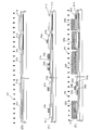
- the configuration of the pixel TFT 105, the holding TFT 204, and the optical sensor TFD 202 in the present embodiment will be described more specifically with reference to FIG.
- a single-gate TFT having an LDD structure is illustrated as the pixel TFT 105 and the holding TFT 204, but the TFT structure is not limited to this.
- the pixel TFT 105, the holding TFT 204, and the optical sensor TFD 202 are all formed on the same substrate 111 through the base films 113 and 114.
- semiconductor layers 130, 140, and 150 formed from the same semiconductor film are provided as active regions.
- the pixel TFT 105 covers the semiconductor layer 130, the gate insulating film 119 formed on the semiconductor layer 130, the gate electrode 135 provided on the gate insulating film 119, and the gate electrode 135 and the semiconductor layer 130. , And source and drain electrodes 137 are provided.
- the semiconductor layer 130 includes a source / drain region 133, a channel region 131 located between these regions, and an LDD region 132 located between the source / drain region 133 and the channel region 131.
- the gate electrode 135 overlaps with the channel region 131 and does not overlap with the LDD region 132.
- the source and drain regions 133 are connected to the source and drain electrodes 137 in contact holes formed in the protective film 130, respectively.
- the holding TFT 204 has an LDD structure similarly to the pixel TFT 105.
- the semiconductor layer 140 includes a gate electrode 145 provided over the semiconductor layer 140 with a gate insulating film 119 interposed therebetween, protective films 120 and 121, and source and drain electrodes 147.
- the semiconductor layer 140 includes a source / drain region 143, a channel region 141, and an LDD region 142 located between the source / drain region 143 and the channel region 141.
- the gate electrode 145 overlaps with the channel region 141 and does not overlap with the LDD region 142.
- the source and drain regions 143 are connected to the source and drain electrodes 147 in contact holes formed in the protective film 140, respectively.
- a light shielding layer 149 is disposed on the substrate 111 side of the semiconductor layer 140 of the holding TFT 204 via insulating films 113 and 114.
- the light shielding layer 149 may be disposed so as to overlap with at least the channel region 141 of the semiconductor layer 140.
- the semiconductor layer 140 is disposed so as to overlap the whole as illustrated.
- the light shielding layer 149 prevents light from entering the semiconductor layer 140 from the substrate 111 side and causing leakage current.
- the light shielding layer 149 is connected to the VLS line, and its potential is fixed. For this reason, the off-leakage current of the holding TFT 204 can be more effectively reduced by the back gate effect.
- the pixel TFT 105 and the holding TFT 204 are both n-channel TFTs.
- the channel regions 131 and 141 of these TFTs are doped with a p-type impurity such as boron in order to adjust the threshold voltage (channel dope).
- concentration of the p-type impurity is separately controlled in consideration of the characteristics required for each TFT and the threshold voltage.
- the on-characteristic changes depending on the set value of the potential of the light shielding layer 149. Specifically, the on-current Ion increases as the potential of the light shielding layer 149 increases, and the on-current Ion decreases as the potential decreases. Accordingly, when the potential of the light shielding layer 149 is set to be negative, the p-type impurity concentration in the channel region 141 of the holding TFT 204 is changed in the channel region 131 of the pixel TFT 105 so that the on-current Ion of the holding TFT 204 satisfies the specification. It is preferable to set it lower than the concentration of the p-type impurity. As a result, while the desired characteristics can be secured in the pixel TFT 105, a decrease in the on-current due to the light shielding layer 149 can be suppressed in the holding TFT 204, and a desired on-characteristic can be obtained.
- the concentration of the n-type impurity in the LDD regions 132 and 142 in the pixel TFT 105 and the holding TFT 204 may be controlled separately in consideration of the characteristics required for each TFT. For example, as described above, when the p-type impurity concentration in the channel region of the holding TFT 204 is kept low, the off-leak current of the holding TFT 204 may not be sufficiently reduced by channel doping. In such a case, the n-type impurity concentration in the LDD region 142 of the holding TFT 204 may be set lower than the n-type impurity concentration in the LDD region 132 of the pixel TFT 105. As a result, the off-leak current can be reduced to a desired range while ensuring the desired characteristics in the pixel TFT 105 and ensuring the on-characteristics in the holding TFT 204.
- the optical sensor TFD 202 includes an n-type region 153, a p-type region 154, a semiconductor layer 150 having an intrinsic region 151 positioned therebetween, and electrodes 157 connected to the n-type region 153 and the p-type region 154, respectively. And.
- the intrinsic region 151 becomes a light receiving region.
- a light shielding layer 159 is provided on the substrate 111 side of the semiconductor layer 150 with insulating films 113 and 114 interposed therebetween.
- the light shielding layer 159 is disposed so as to overlap at least the intrinsic region 151 of the semiconductor layer 150.
- the light-blocking layer 159 can prevent light from being incident on the intrinsic region 151 from the substrate 111 side to generate photocurrent, so that light incident on the intrinsic region 151 from above the semiconductor layer 150 can be sensed more accurately. become.
- intrinsic region refers to a region sandwiched between a p-type region and an n-type region and having a lower impurity concentration (that is, higher resistance) than these regions. Therefore, the intrinsic region may be a region made of an intrinsic semiconductor, or a region where p-type or n-type impurities are implanted at a lower concentration than the p-type region or the n-type region.
- the potential of the light shielding layer 159 is fixed. If the light shielding layer 159 is floating, the light shielding layer 159 may be charged and the characteristics of the optical sensor TFD 202 may change.
- the light shielding layer 159 may be electrically connected to the light shielding layer 149 below the holding TFT 204 and may be connected to the VLS line. This is advantageous because the potential of the light shielding layers 149 and 159 can be fixed using a common line.
- the buffer TFT 208 is also formed using a semiconductor layer formed of the same semiconductor film as these TFD and TFT. It is preferable.
- the structure of the buffer TFT 208 may be, for example, a single drain structure that does not have an LDD region.
- the signal storage capacitor 206 is configured by using a gate electrode layer and a semiconductor layer formed of the semiconductor film as electrodes, and the capacitor may be formed of a gate insulating film.
- the p-type region 154 in the optical sensor TFD 202 is connected to the RST signal line, and the n-type region 153 is connected to the drain electrode 147 of the holding TFT 204.
- the gate electrode 145 of the holding TFT 204 is connected to the CLK signal line, and the source electrode 147 is connected to the lower electrode (semiconductor layer) in the capacitor 206, and is connected to the RWS signal line through the capacitor 206.
- the source electrode 147 of the holding TFT 204 is also connected to the gate electrode of the buffer TFT 208.
- the drain electrode of the buffer TFT 208 is connected to the VDD signal line, and the source electrode is connected to the output signal line.
- the configuration of the semiconductor device of the present embodiment is not limited to the configuration shown in FIG. In FIG. 1A, one photosensor unit 200 is provided for two color display pixels 109a and 109b, but the number (density) of photosensor units with respect to the number of pixels depends on the resolution. Can be selected as appropriate.
- one photosensor unit 200 may be provided for one or three or more color display pixels.
- One photosensor unit 200 may be provided for one primary color pixel or a set of a plurality of pixels.
- FIG. 1C shows a TFT having an LDD structure as the pixel TFT 105 and the holding TFT 204, but these TFTs may not have the LDD structure. Moreover, you may have a multi-gate structure. Further, the light shielding layers 149 and 159 do not have to be provided on the back side of the holding TFT 204 or the optical sensor TFD 202.
- Each optical sensor unit may have a plurality of optical sensors TFD.
- another optical sensor TFD having a detectable wavelength range different from that of the optical sensor TFD 202 may be provided.
- a plurality of optical sensors TFD of the same type may be connected in parallel to increase the output.
- FIG. 2 is a schematic cross-sectional view showing an example of an active matrix type touch panel liquid crystal display device.
- the same components as those in FIG. 1 are denoted by the same reference numerals.
- the liquid crystal display device 1000 includes a liquid crystal module 180 and a backlight 170 disposed on the back side of the liquid crystal module 180.
- the liquid crystal module 180 includes a rear substrate 111 having translucency, a front substrate 171 disposed so as to face the rear substrate, and a liquid crystal layer 177 provided between these substrates.
- Polarizers 175 are provided on the viewer side of the front substrate 171 and the back side of the back substrate 111, respectively.
- the liquid crystal module 180 includes a plurality of pixels (primary color pixels), and each pixel includes a pixel electrode (not shown) and a pixel TFT 105 connected to the pixel electrode.
- An optical sensor unit including the optical sensor TFD 202 is disposed adjacent to each of the color display pixels including three primary color (RGB) pixels.
- a color filter (not shown) is arranged on the observer side of each pixel, but it is preferable that no color filter is provided on the observer side of the optical sensor unit. This is because if the color filter is provided on the observer side of the optical sensor unit, the sensitivity of the optical sensor TFD 202 constituting the optical sensor unit may be reduced.
- a light shielding layer 159 is disposed between the optical sensor TFD 202 and the backlight 170. Therefore, the light 191 from the backlight 170 is blocked by the light blocking layer 159 and does not enter the photosensor TFD 202 from the back surface (from the back substrate 111 side). Note that the light shielding layer 159 may be arranged so that at least the light of the backlight 170 does not enter the intrinsic region of the optical sensor TFD 202.
- the light sensor unit can sense an object in contact with the screen by using external light 193 incident on the display device 1000.
- sensing of an object in contact with the screen may be performed using light emitted from the backlight 170 (backlight light).
- backlight light may be configured such that sensing can be performed using both the external light 193 and the backlight light 191.
- sufficient external light 193 may not enter the display area depending on the use environment of the display device 1000. Even in such a case, sensing using the backlight light 191 can be performed.
- Sensing using the backlight light 191 can be performed as follows.
- the backlight light 191 passes through the display panel and reaches the panel surface.
- the light is reflected by an object such as a finger pad, the light enters the optical sensor unit arranged in the display area. Therefore, an object in contact with the screen can be detected by sensing light incident on the optical sensor unit.
- the backlight light 191 it is necessary to use a TFD that can detect the backlight light 191 as the optical sensor TFD 202.
- the backlight 170 preferably emits infrared light in addition to visible light.
- the optical sensor unit can also perform sensing using infrared light emitted from the backlight light 170.
- sensing using infrared light is advantageous.
- the backlight visible light When sensing is performed using visible light (referred to as “backlight visible light”) emitted from the backlight, the backlight that has passed through the liquid crystal layer 177 is displayed in the pixel displaying “black” in the display panel. Visible light is blocked by the polarizing plate on the viewer side and does not reach the object in contact with the screen. For this reason, when the backlight visible light is used, the sensing sensitivity may be reduced depending on the display.
- the above-described display dependency problem can be overcome. Unlike visible light, infrared light is transmitted through the polarizing plate even in pixels where black is displayed. For this reason, when infrared light is used, sensing can be performed with a predetermined sensitivity regardless of display.
- a TFD capable of detecting infrared light (wavelength: 0.7 ⁇ m or more, energy: 1.7 eV or less) is used as the optical sensor TFD 202.
- the optical sensor TFD 202 may be capable of detecting not only infrared light but also visible light. When sensing mainly by infrared light, it is preferable that the optical sensor TFD 202 can detect infrared light with higher sensitivity than visible light.
- a first photosensor TFD that can detect visible light with high sensitivity and a second photosensor that can detect infrared light in each photosensor unit.
- a TFD may be connected in parallel.
- the light wavelength range that can be detected by the optical sensor TFD includes, for example, the thickness of the semiconductor layer, the crystal grain size, the thickness of each layer above the semiconductor layer, and the thickness of the interlayer film (base coat) between the semiconductor layer and the light shielding layer. It can be adjusted as appropriate.
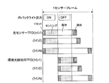
- Holding period When the holding TFT 204 is turned off after a lapse of a predetermined period, the potential of the node 209 that has become negative due to the light leakage current is kept lowered.
- Reading period At the time of reading, the gate voltage applied to the buffer TFT 208 is changed by setting the RWS potential to be positive (12 V). A VDD signal is applied from the VDD signal line to the drain side of the buffer TFT 208. When the gate voltage fluctuates as described above, the value of the current flowing to the output (OUT) signal line connected to the source side changes, so that the electrical signal can be extracted from the output signal line.
- This embodiment can also be applied to a sensing method using only infrared light emitted from the backlight.
- This sensing method is described in, for example, International Publication No. 2011/040090, International Publication No. 2011/040091, International Publication No. 2011/040093 and the like by the present applicant.
- the above application describes a method of removing the influence of infrared rays contained in ambient light by providing a TFD for detecting ambient light in addition to the above-described optical sensor TFD 202.
- the backlight is turned on and sensing is performed with the optical sensor TFD.
- the optical sensor TFD not only backlight light (signal light) but also ambient light is detected.
- the backlight is turned off, and only the ambient light is detected using the ambient light detection TFD.
- a period from when sensing is performed by the optical sensor TFD to when a sensor signal is read out is a “holding period”.
- the potential of the node 209 can be maintained in this holding period by turning off the holding TFT 204 (2).
- the time for turning on the backlight can be shortened compared to the method in which the backlight is always on, so that power consumption can be reduced.
- This embodiment is not limited to a touch panel liquid crystal display device, but can also be applied to a display device with an image sensor or fingerprint sensor function.
- the optical sensor unit 200 described above can also be used as an image sensor or a fingerprint sensor.
- a resolution higher than that of a touch sensor is generally required in order to detect an image or a fingerprint pressed against the screen. Since the resolution increases as the number of photosensor units for the pixel increases, the number of photosensor units may be adjusted as appropriate according to the application. Note that as shown in FIG. 1A, if one optical sensor unit is arranged for two color display pixels, a sufficient resolution capable of reading an image such as a business card can be secured.
- the optical sensor unit can also function as a color image sensor.
- the relationship between the potential of the light shielding layer, the concentration of the P-type impurity (in this case, boron) in the channel region, the resistance value of the LDD region, and the TFT characteristics was examined. To do.
- FIG. 3 is a graph showing the relationship between the potential Vls of the light shielding layer of the holding TFT and the on-current Ion when the boron injection amount into the channel region is changed.
- the horizontal axis of FIG. 3 is the potential (fixed) (V) of the light shielding layer, and the vertical axis is the on-current Ion (A) when the drain-source voltage Vds is 0.1 V and the gate-source voltage Vgs is 5 V.
- a straight line C1 in FIG. 3 is a graph showing the relationship between the potential Vls of the light shielding layer and the on-current Ion when the boron concentration in the channel region is 2.6 ⁇ 10 17 / cm 3 .
- the straight lines C2 and C3 indicate the potential Vls of the light shielding layer and the on-current Ion when the boron concentration in the channel region is 3.8 ⁇ 10 17 / cm 3 and 5.0 ⁇ 10 17 / cm 3 , respectively. It is a graph which shows the relationship.
- the on-current Ion varies depending on the potential Vls of the light shielding layer and the boron concentration of the channel region. Specifically, the on-current Ion decreases as the potential Vls of the light shielding layer decreases. Further, as the boron concentration (boron implantation amount) in the channel region increases, the on-current Ion decreases. It is considered that when the boron concentration is high, carriers are scattered by impurities (boron) and mobility is lowered.
- the decrease in the on-current Ion due to the provision of the light shielding layer can be compensated by suppressing the boron concentration low.
- a desired on-current Ion for example, 1 ⁇ 10 ⁇ 7 A or more
- the boron concentration in the channel region to be lower than the C1 concentration. it can.
- the boron concentration in the channel region of the holding TFT is controlled independently of other TFTs. Therefore, regardless of the characteristics required for other TFTs, the boron concentration in the channel region of the holding TFT can be optimized according to the desired ON characteristics and the potential Vls of the light shielding layer.
- the ON characteristic is not lowered by the potential Vls of the light shielding layer.
- the light shielding layer is not formed, light is incident on the channel region of the semiconductor layer of the TFT, so that a leakage current is generated and the off characteristics of the TFT may be deteriorated.
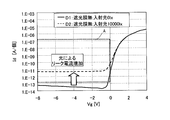
- FIG. 4 is a graph illustrating the Vg-Id characteristics of a TFT having no light shielding layer.
- the leakage current when the gate voltage Vg is 0 or less is, for example, 1 ⁇ 10 ⁇ 13 A / piece or more (range A shown in FIG. 4)
- the sensing characteristics by the optical sensor unit may deteriorate.
- the leakage current increases more than when light hardly enters the channel region (illuminance: 0 lx, curve D1).
- the leakage current due to light increases, for example, to near 1 ⁇ 10 ⁇ 11 A / piece and falls within the range A. Accordingly, it can be seen that it is preferable to sufficiently shield at least the channel region of the holding TFT.
- FIG. 5 is a graph illustrating the relationship between the resistance value Loff of the LDD region and the off-current Ioff in the holding TFT.
- the horizontal axis represents the resistance value Loff (k ⁇ / ⁇ ) of the LDD region. The higher the impurity concentration (here, phosphorus concentration) in the LDD region, the lower the resistance value Loff.
- the vertical axis represents the off current Ioff (A) when the drain-source voltage Vds is 7 V and the gate-source voltage Vgs is ⁇ 3 V.
- the off-current Ioff when the off-current Ioff is, for example, 4 ⁇ 10 ⁇ 13 A or more (range B shown in FIG. 5), the sensing characteristics of the optical sensor unit may be deteriorated.
- the off-current Ioff can be reduced by increasing the resistance value Loff of the LDD region.
- the resistance value Loff when the resistance value Loff is 50 k ⁇ / ⁇ or more, the off-current Ioff can be sufficiently smaller than 4 ⁇ 10 ⁇ 13 A.
- the resistance value Loff is 10 k ⁇ / ⁇
- the off-current Ioff increases to 6 ⁇ 10 ⁇ 13 A and enters the range B.
- the resistance value Loff of the LDD region of the holding TFT independently of other TFTs, the resistance value Loff of the LDD region can be optimized regardless of the characteristics required for the other TFTs. The required off characteristics can be secured.
- the holding TFT is provided with a light shielding layer, and the amount of boron injected into the channel region of the holding TFT is optimized separately from the other TFTs. It is possible to achieve the required characteristics. If necessary, the amount of phosphorus implanted into the LDD region of the holding TFT may be optimized separately from the other TFTs.
- the off-leakage current may not be sufficiently reduced by channel doping.
- the off-leakage current can be reduced to a desired range. Therefore, it is possible to achieve both desired off characteristics and on characteristics.
- the present embodiment is a display device including an optical sensor unit.
- the configuration of the display device of the present embodiment will be described using a liquid crystal display device with a touch sensor as an example.
- the display device of the present embodiment has a display area and a frame area located around the display area.
- the display area includes a plurality of pixels and a plurality of photosensor units.
- the configuration of the pixel and the optical sensor unit may be the same as the configuration described above in the first embodiment. That is, each pixel includes a pixel electrode and a pixel TFT.
- Each photosensor unit includes at least one photosensor TFD, a capacitor, and a holding TFT.
- a display drive circuit for driving each pixel is provided in the frame region.
- the drive circuit generally includes an n-type TFT and a p-type TFT.
- the TFT constituting the driving circuit is referred to as a driving circuit TFT.
- the driving circuit TFT, pixel TFT, holding TFT, and optical sensor TFD are formed on the same substrate. Moreover, it is preferable that these TFT and TFD have the semiconductor layer formed from the same semiconductor film as an active region. Moreover, it is preferable that these TFT and TFD are formed by a common process.
- the driving circuit TFT and the holding TFT have different characteristics such as threshold voltage and off-leakage characteristics.
- the characteristics of these TFTs can be controlled by the TFT structure, the impurity concentration of the channel region, the impurity concentration of the LDD region, the presence / absence of a light shielding layer, and the like, as in the above embodiment. Note that the characteristics of each TFT may be different among the driving circuit TFT, the holding TFT, and the pixel TFT.
- a base coat insulating film is formed so as to cover the light shielding layers 302s and 302d.
- the light shielding layers 302 s and 302 d are arranged so as to block light from the substrate rear surface direction with respect to the holding TFT and the TFD, respectively.
- the light shielding layers 302s and 302d are formed as follows, for example.
- a metal film or an insulating film serving as a light shielding layer is formed on the surface of the substrate 301 by a CVD (Chemical Vapor Deposition) method, a sputtering method, or the like.
- the metal film a film containing an element such as Ta, Ti, W, Mo, or Al as a main component can be used.
- a Si film can be used as the insulating film.
- the thickness of the metal film or insulating film is preferably 50 nm or more, for example.
- the base coat insulating film for example, a silicon oxide film or a silicon nitride film may be formed by a CV method.
- the base coat insulating film may be a single layer or may have a multilayer structure.
- the thickness of the base coat insulating film is, for example, not less than 100 nm and not more than 500 nm.
- a silicon nitride film 303 and a silicon oxide film 304 are formed in this order by plasma CVD.
- the light shielding layer is arrange
- a light shielding layer may be disposed on the back side of another TFT.
- a semiconductor film 306 is formed over the silicon oxide film 304.
- a crystalline silicon film is formed as the semiconductor film 306.
- the thickness of the semiconductor film 306 is, for example, not less than 40 nm and not more than 300 nm.
- the crystalline silicon film may be formed by depositing an amorphous silicon film on the silicon oxide film 304 and crystallizing it.
- the crystallization method is not particularly limited. For example, crystallization may be performed using a catalyst element, or crystallization may be performed at a low temperature using an excimer laser or the like.
- an amorphous silicon film (thickness: 20 nm or more and 150 nm or less) is formed by a known method such as a plasma CVD method or a sputtering method. Thereafter, a catalytic element for promoting crystallization is added to a part or the whole of the surface of the amorphous silicon film.
- a thin film here, a nickel film
- a catalytic element is formed on an amorphous silicon film by vapor deposition or sputtering.
- the addition of the catalyst element may be performed by applying an aqueous solution (nickel acetate aqueous solution) containing about 1 to 10 ppm, for example, 5 ppm of the catalyst element (nickel) in terms of weight by spin coating.
- an aqueous solution nickel acetate aqueous solution
- nickel nickel
- Multiple kinds of elements may be used. Although the catalytic effect is smaller than these elements, ruthenium (Ru), rhodium (Rh), osmium (Os), iridium (Ir), platinum (Pt), gold (Au), etc.
- amorphous silicon film is crystallized to obtain a crystalline silicon film.
- laser annealing is performed on the amorphous silicon film, the nickel thin film and the amorphous silicon film are reacted, and crystalline silicon is formed at the interface between these films. Thereafter, the unreacted nickel film and the nickel silicide layer are removed by etching or the like. Next, laser annealing is further performed on the remaining silicon film, and further crystallization is performed. In this way, a crystalline silicon film is obtained.
- heat treatment may be performed in an inert atmosphere, for example, in a nitrogen atmosphere using a furnace instead of laser annealing.
- crystallization may be performed by an RTA (Rapid Thermal Annealing) apparatus using a lamp as a heat source.
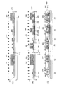
- the semiconductor layer 311n that becomes the active region (source / drain region, channel region) of the n-type TFT for the drive circuit, the semiconductor layer 311p that becomes the active region of the p-type TFT for the drive circuit, and the active region of the pixel TFT The semiconductor layer 311t that becomes the active region of the holding TFT, and the semiconductor layer 311d that becomes the active region (n + type / p + type region, intrinsic region) of the photosensor TFD are formed.
- the semiconductor layers 311t, 311s, and 311d are arranged in a region serving as a display region of the substrate 301, and the semiconductor layers 311n and 311p are arranged outside the region serving as a display region.
- a gate insulating film 313 is formed to cover the semiconductor layers 311n, 311p, 311t, 311s, and 311d.
- a silicon oxide film or a silicon nitride film may be formed by a CVD method, for example.
- plasma CVD may be performed using SiH 4 and N 2 O (or O 2 ) as a source gas.
- the gate insulating film 313 may be a single layer or may have a multilayer structure. The thickness of the gate insulating film 313 is, for example, not less than 10 nm and not more than 120 nm.
- p-type impurities 315 such as boron (B) and indium (In) are ion-implanted into each semiconductor layer.
- ion implantation is performed by setting the implantation energy to 10 KeV or more and 80 KeV or less and the dose amount to 5 ⁇ 10 11 (ion / cm 2 ) or more and 5 ⁇ 10 12 (ion / cm 2 ) or less.
- the concentration of p-type impurities in these semiconductor layers after implantation is preferably 5 ⁇ 10 16 (pieces / cm 3 ) or more and 5 ⁇ 10 17 (pieces / cm 3 ) or less.
- the amount of p-type impurity 315 implanted into the semiconductor layers 311n, 311p, 311t, 311s, and 311d is varied.
- a plurality of ion implantation steps with different implantation conditions may be performed using different implantation masks (resist masks).
- the implantation amount for each semiconductor layer can be made different.
- the concentration of the p-type impurity is adjusted so that desired off characteristics and on characteristics can be obtained for each TFT.
- the concentration of the p-type impurity is optimized in consideration of the potential (FIG. 3). Note that the p-type impurity may not be implanted into the semiconductor layer 311p of the p-type TFT or the semiconductor layer 311d of the optical sensor TFD.
- the boron dose of the semiconductor layer 311s to be the holding TFT is set to 2 ⁇ 10 12 / cm 2 or more and 4 ⁇ 10 12 / cm 2
- the boron dose of the semiconductor layer 311t to be the pixel TFT is 3.8 ⁇ 10 12 / cm 2.
- the impurity concentration (boron concentration) of the channel region of the holding TFT manufactured by this method is 2 ⁇ 10 17 / cm 3 or more and 4 ⁇ 10 17 / cm 3 or less
- the impurity concentration (boron concentration) of the channel region of the pixel TFT is 3.8 ⁇ 10 17 / cm 3
- gate electrodes 316n, 316p, 316t, and 316s are formed over the gate insulating film 313 so as to overlap with part of the TFT semiconductor layers 311n, 311p, 311t, and 311s, respectively. To do.
- an auxiliary capacitor upper electrode 316c is formed on the semiconductor layer 311t.
- two gate electrodes 316t are formed in the semiconductor layer 311t of the pixel TFT (double gate structure), and one gate electrode is formed in the semiconductor layer of the other TFT.
- the gate structure is not limited to this.
- Two or three gate electrodes may be formed on the semiconductor layer 311s of the holding TFT to form a double gate structure or a triple gate structure.
- the gate electrodes 316n, 316p, 316t, and 316s are formed by depositing a conductive film on the gate insulating film 313 using a sputtering method, a vacuum evaporation method, or the like, and patterning the conductive film.
- the conductive film is preferably a metal film containing an element such as W, Ta, Ti, Mo, or Al as a main component.
- the thickness of the conductive film is, for example, 200 nm or more and 600 nm or less.
- p-type impurities 318 are ion-implanted into a part of the semiconductor layer 311p of the p-type TFT for driver circuit and the semiconductor layer 311d of the optical sensor TFD, and a p-type diffusion layer is formed.
- resist masks 325n, 325t, 325s which cover the entire semiconductor layers 311n, 311t, and 311s and regions that become the n-type region (n layer) and the intrinsic region (i layer) of the semiconductor layer 311d, 325d is formed.
- a p-type impurity 318 such as boron (B) or indium (In) is ion-implanted.
- the p-type impurity 318 is implanted into a region of the semiconductor layer 311p that is not covered with the gate electrode 316p to form a source / drain region 327p.
- the implantation conditions in this step are not particularly limited.
- ion implantation is performed with the implantation energy set to 10 KeV or more and 80 KeV or less and the dose amount set to 5 ⁇ 10 14 (ion / cm ⁇ 2 ) or more and 2 ⁇ 10 16 (ion / cm ⁇ 2 ) or less.
- the concentration of the p-type impurity in the source / drain region 327p and the p-type region 340d is preferably 1.5 ⁇ 10 20 (pieces / cm 3 ) or more and 3 ⁇ 10 21 (pieces / cm 3 ) or less.
- the semiconductor layer 311n of the driver circuit n-type TFT, the semiconductor layer 311t of the pixel TFT, the semiconductor layer 311s of the holding TFT, and a part of the semiconductor layer 311d of the photosensor TFD are formed.
- An n-type impurity 320 is implanted to form an n-type diffusion layer.
- resist masks 326p and 326d that cover the entire semiconductor layer 311p and the p-type region and intrinsic region of the semiconductor layer 311d are formed.
- an n-type impurity 320 such as phosphorus (P) or arsenic (As) is ion-implanted.
- the n-type impurity 320 is implanted into a region of the semiconductor layers 311n, 311t, and 311s that is not covered with the gate electrodes 316n, 316t, and 316s.
- an n-type impurity 320 is implanted into a region of the semiconductor layer 311d that is not covered with the resist mask 326d.
- the resist masks 326p and 326d are removed.
- the implantation conditions in this step are not particularly limited.
- ion implantation is performed by setting the implantation energy to 10 KeV to 100 KeV and the dose to 1 ⁇ 10 12 (ion / cm 2 ) to 1 ⁇ 10 14 (ion / cm 2 ).
- the concentration of the n-type impurity in the n-type diffusion layer is preferably 1 ⁇ 10 17 (pieces / cm 3 ) or more and 1 ⁇ 10 19 (pieces / cm 3 ) or less.
- n-type impurity 322 is further implanted into a region to be an n-type region of the TFD semiconductor layer 311d to form a high concentration n-type region.
- resist masks 330p, 330t, and 330s that cover the entire semiconductor layer 311p, a region that becomes an LDD region of the semiconductor layers 311t and 311s, and a region that becomes a p-type region and an intrinsic region of the semiconductor layer 311d. , 330d.
- n-type impurities 322 such as phosphorus (P) and arsenic (As) are ion-implanted.
- P phosphorus
- As arsenic
- n-type impurities 322 are implanted into regions of the semiconductor layers 311t and 311s that are not covered by the resist masks 330t and 330s and the gate electrodes 316t and 316s to become source / drain regions 327t and 327s, respectively.
- regions that are not covered with the gate electrodes 316t and 316s but are covered with the resist masks 330s and 330t and into which the n-type impurity 322 is not implanted become LDD regions 329t and 329s.
- the regions that overlap with the gate electrodes 316t and 316s and are not implanted with the n-type impurities 320 and 322 are channel regions 328t and 328s. The portion of the semiconductor layer 311t that overlaps with the upper electrode 316c becomes the lower electrode 344c of the auxiliary capacitor.
- an n-type impurity 322 is implanted into a region of the semiconductor layer 311d that is not covered with the resist mask 330d, whereby an n-type region 342d is formed.
- the resist masks 330p, 330t, 330s, and 330d are removed.
- the implantation conditions in this step are not particularly limited.
- ion implantation is performed with the implantation energy set to 10 KeV or more and 100 KeV or less, and the dose amount set to 5 ⁇ 10 14 (ion / cm 2 ) or more and 1 ⁇ 10 16 (ion / cm 2 ) or less.
- the concentration of the n-type impurity in the n-type diffusion layer is preferably 1.5 ⁇ 10 20 (pieces / cm 3 ) or more and 3 ⁇ 10 21 (pieces / cm 3 ) or less.
- the LDD region 329t of the pixel TFT and the LDD region 329s of the holding TFT have the same impurity concentration, but these impurity concentrations may be different.
- the ion implantation step for forming the LDD region (FIG. 8G) is divided into two steps, and the ion implantation step for forming the LDD region of the pixel TFT and the LDD region of the holding TFT are formed. Therefore, the ion implantation process may be performed, and the implantation conditions of each process may be varied.
- the implantation amounts for the semiconductor layers 311t and 311s can be changed using a gray-tone mask.
- the n-type impurity concentration of each LDD region is not particularly limited, but as described later, when the resistance of the LDD region is increased by keeping the n-type impurity concentration low, the off-leakage current can be further reduced. However, when the resistance of the LDD region is increased, the on-current is also decreased. For this reason, it is preferable that the n-type impurity concentration in the LDD region is optimized according to the on characteristics and the off characteristics required for each TFT.
- an interlayer insulating film 350 is formed.
- a plasma CVD method may be performed using SiH 4 and N 2 O (or O 2 ) as a source gas.
- the interlayer insulating film 350 may be a single layer or may have a multilayer structure.
- a silicon nitride film 351 and a silicon oxide film 352 are formed in this order as the interlayer insulating film 350. If necessary, heat treatment for hydrogenation may be performed.
- a conductive film is deposited on the interlayer insulating film 350 and inside the contact hole and patterned.
- TFT electrode / wiring 354n, 354p, 354t, 354s and TFD electrode / wiring 354d are obtained.
- the conductive film it is preferable to use a metal film mainly composed of elements such as Ta, Ti, W, Mo, and Al.
- the conductive film can be formed by a sputtering method, a vacuum evaporation method, or the like.
- the conductive film may be a single layer or may have a stacked structure.
- the n-type TFT 361 for the drive circuit, the p-type TFT 362 for the drive circuit, the pixel TFT 363, the auxiliary capacitor 364, the holding TFT 365, and the optical sensor TFD 366 are obtained.
- a planarizing film may be provided on these TFTs and TFDs.
- the planarizing film it is necessary to form an opening for electrically connecting a pixel electrode to be formed later and the pixel TFT.
- the material of the planarizing film may be a photosensitive resin. In this case, an opening can be formed above the pixel TFT by photolithography.
- a pixel electrode is formed on the planarizing film.
- a transparent conductive material for example, ITO, IZO, etc.
- the manufacturing method of the semiconductor device of this embodiment is not limited to the above method.
- a TFT having a single drain structure is formed as the driving circuit TFT, but a TFT having a GOLD (Gate Overlapped LDD) structure may be formed.
- GOLD structure refers to a structure in which, for example, LDD regions are overlapped by gate electrodes.
- a TFT having a GOLD structure when a voltage is applied to the gate electrode, electrons serving as carriers are accumulated in the LDD region where the gate electrode overlaps. Therefore, since the resistance of the LDD region can be reduced, it is possible to suppress a decrease in the current driving capability of the TFT.
- a TFT with a GOLD structure has a drawback that off-leakage current is larger than a TFT with an LDD structure (a structure in which a gate electrode and an LDD region do not overlap), and is not suitable for a pixel TFT or a holding TFT.
- LDD structure a structure in which a gate electrode and an LDD region do not overlap
- the crystallization method using the catalytic element has been described in detail.
- the amorphous semiconductor film can be crystallized by irradiating a laser (laser crystallization).
- the crystallized semiconductor film has higher crystallinity than a semiconductor film crystallized by another method (for example, laser crystallization).
- a TFT is formed using a semiconductor layer with high crystallinity, the rising characteristic (subthreshold characteristic) when the TFT is on can be improved. That is, the change of the drain current with respect to the gate-source voltage near the threshold voltage can be made steeper.
- the semiconductor layer formed from the semiconductor film crystallized using the catalytic element contains the catalytic element.
- at least the channel region of the semiconductor layer is mainly composed of a region in which the ⁇ 111> crystal zone plane of the crystal is oriented. The reason for this will be described below.
- the plane orientation of the crystalline semiconductor film is (111) due to the influence of an insulator underlying the semiconductor film (particularly in the case of amorphous silicon dioxide). ) Easy to face.
- the semiconductor compound of the catalytic element becomes a driving force for crystal growth, and the adjacent amorphous region is unidirectionally formed. Crystallizes one after another. At this time, since the catalytic element compound has a property of growing strongly in the ⁇ 111> direction, a ⁇ 111> crystal zone surface appears.
- 50% or more of the region where the ⁇ 111> crystal zone plane of the semiconductor layer is oriented is a (110) or (211) oriented region.
- the size (domain diameter) of each crystal domain is, for example, 2 ⁇ m or more and 10 ⁇ m or less.
- the plane orientation, the ratio of plane orientation, and the domain diameter of the crystal domain are values measured by EBSP measurement.
- the semiconductor device of the present invention is not limited to a display device including an optical sensor unit, and may be an image sensor.
- the configuration of the image sensor to which the present invention is applied will be briefly described below.
- the image sensor includes a plurality of light receiving units arranged two-dimensionally and an image information generation unit that generates image information.
- Each light receiving portion may have a structure similar to that of the pixel shown in FIG. Or you may be comprised from three pixels (RGB pixel).
- Each light receiving unit includes the photosensor unit as described above.
- the image information generation unit generates a sensing signal generated by the optical sensor unit of each light receiving unit and image information associated with the position of each light receiving unit. Thereby, the image read by the image sensor can be formed or authenticated.
- the configuration of the optical sensor unit in the present invention is not limited to the configuration shown in FIG.
- a plurality of optical sensors TFD may be connected in parallel to increase the output.
- FIG. 9 is a diagram illustrating an example of an active matrix substrate including an optical sensor unit 400 having a plurality of optical sensors.
- the optical sensor unit 400 includes optical sensors TFDs 402a, 402b, and 402c, a holding TFT 404, capacitors 406a and 406b, and a buffer TFT 408 that are connected in parallel. Since the photosensor unit 400 uses the three photosensors TFD, a larger photocurrent can be generated, so that deterioration of sensing characteristics due to off-leakage of the holding TFT can be suppressed. In this example, one photosensor unit 400 is arranged for 12 pixels, that is, 4 color pixels.
- the holding TFT in this embodiment may have a multi-gate structure having a plurality of gate electrodes.
- FIG. 10 is a plan view showing a part of an active matrix substrate having a holding TFT having a triple gate structure.
- the gate electrode gate wiring meanders and overlaps the semiconductor layer at three places, and three channel regions are formed in the semiconductor layer. With such a configuration, the off-leakage current can be reduced more effectively.
- the pixel TFT, the holding TFT, and the driving circuit TFT can be optimized according to their respective uses and requirements, and the required device characteristics can be realized. Therefore, it is possible to increase the sensor sensitivity of the optical sensor unit and realize higher quality display.
- the display device as described above can be manufactured by a process with a low cost and a small number of steps.
- a doping step for forming the source and drain regions of the pixel TFT, the holding TFT, and the driving circuit TFT and a doping step for forming the n-type or p-type region of the photosensor TFD can be further simplified.
- the present invention can be widely applied to a semiconductor device provided with an optical sensor unit having an optical sensor TFD, or electronic devices in various fields having such a semiconductor device.
- the present invention may be applied to an active matrix liquid crystal display device or an organic EL display device.
- Such a display device can be used for a display screen of a mobile phone or a portable game machine, a monitor of a digital camera, or the like. Therefore, the present invention can be applied to all electronic devices in which a liquid crystal display device or an organic EL display device is incorporated.
- the present invention can be suitably used particularly for display devices such as active matrix liquid crystal display devices and organic EL display devices, image sensors, photosensors, or electronic devices that combine them.
- display devices such as active matrix liquid crystal display devices and organic EL display devices, image sensors, photosensors, or electronic devices that combine them.
- the present invention can be applied to an image sensor including a photosensor using TFD and a driving circuit using TFT.
Landscapes
- Physics & Mathematics (AREA)
- Engineering & Computer Science (AREA)
- Power Engineering (AREA)
- General Physics & Mathematics (AREA)
- Microelectronics & Electronic Packaging (AREA)
- Theoretical Computer Science (AREA)
- Computer Hardware Design (AREA)
- Condensed Matter Physics & Semiconductors (AREA)
- General Engineering & Computer Science (AREA)
- Nonlinear Science (AREA)
- Electromagnetism (AREA)
- Chemical & Material Sciences (AREA)
- Mathematical Physics (AREA)
- Crystallography & Structural Chemistry (AREA)
- Human Computer Interaction (AREA)
- Optics & Photonics (AREA)
- Liquid Crystal (AREA)
- Thin Film Transistor (AREA)
- Solid State Image Pick-Up Elements (AREA)
- Devices For Indicating Variable Information By Combining Individual Elements (AREA)
Abstract
Priority Applications (4)
| Application Number | Priority Date | Filing Date | Title |
|---|---|---|---|
| CN201180019503.8A CN102859693B (zh) | 2010-04-16 | 2011-04-15 | 半导体装置 |
| US13/641,186 US8803151B2 (en) | 2010-04-16 | 2011-04-15 | Semiconductor device |
| EP11768962.0A EP2560207A4 (fr) | 2010-04-16 | 2011-04-15 | Dispositif à semiconducteur |
| JP2012510717A JP5512800B2 (ja) | 2010-04-16 | 2011-04-15 | 半導体装置 |
Applications Claiming Priority (2)
| Application Number | Priority Date | Filing Date | Title |
|---|---|---|---|
| JP2010095136 | 2010-04-16 | ||
| JP2010-095136 | 2010-04-16 |
Publications (1)
| Publication Number | Publication Date |
|---|---|
| WO2011129441A1 true WO2011129441A1 (fr) | 2011-10-20 |
Family
ID=44798809
Family Applications (1)
| Application Number | Title | Priority Date | Filing Date |
|---|---|---|---|
| PCT/JP2011/059410 WO2011129441A1 (fr) | 2010-04-16 | 2011-04-15 | Dispositif à semiconducteur |
Country Status (5)
| Country | Link |
|---|---|
| US (1) | US8803151B2 (fr) |
| EP (1) | EP2560207A4 (fr) |
| JP (1) | JP5512800B2 (fr) |
| CN (1) | CN102859693B (fr) |
| WO (1) | WO2011129441A1 (fr) |
Cited By (3)
| Publication number | Priority date | Publication date | Assignee | Title |
|---|---|---|---|---|
| CN103533263A (zh) * | 2012-07-03 | 2014-01-22 | 三星电子株式会社 | 图像传感器芯片、操作方法和包括图像传感器芯片的系统 |
| JP2015041629A (ja) * | 2013-08-20 | 2015-03-02 | ソニー株式会社 | 放射線撮像装置および放射線撮像表示システム |
| WO2015141777A1 (fr) * | 2014-03-20 | 2015-09-24 | シャープ株式会社 | Dispositif de détection de lumière |
Families Citing this family (26)
| Publication number | Priority date | Publication date | Assignee | Title |
|---|---|---|---|---|
| DE102011011767A1 (de) * | 2011-02-18 | 2012-08-23 | Fresenius Medical Care Deutschland Gmbh | Medizintechnisches Gerät mit Mehrfunktionsdisplay |
| KR101896666B1 (ko) * | 2012-07-05 | 2018-09-07 | 삼성전자주식회사 | 이미지 센서 칩, 이의 동작 방법, 및 이를 포함하는 시스템 |
| US9454265B2 (en) | 2013-09-23 | 2016-09-27 | Qualcomm Incorporated | Integration of a light collection light-guide with a field sequential color display |
| US20150084994A1 (en) * | 2013-09-23 | 2015-03-26 | Qualcomm Incorporated | Touch-enabled field-sequential color (fsc) display using a light guide with light turning features |
| CN103715267A (zh) * | 2013-12-30 | 2014-04-09 | 京东方科技集团股份有限公司 | 薄膜晶体管、tft阵列基板及其制造方法和显示装置 |
| CN104658463A (zh) * | 2015-03-09 | 2015-05-27 | 合肥京东方光电科技有限公司 | 一种显示面板的设置方法和设置系统 |
| CN106325987B (zh) * | 2015-07-03 | 2020-11-20 | 联想(北京)有限公司 | 一种控制方法及电子设备 |
| CN106067018B (zh) * | 2016-08-08 | 2019-01-04 | 京东方科技集团股份有限公司 | 一种指纹识别显示面板及显示装置 |
| CN107134460B (zh) | 2017-04-11 | 2019-08-02 | 深圳市华星光电半导体显示技术有限公司 | 显示装置及其goa电路 |
| CN107123654A (zh) * | 2017-05-26 | 2017-09-01 | 京东方科技集团股份有限公司 | 阵列基板及其制备方法和显示装置 |
| CN107066162B (zh) | 2017-05-27 | 2020-03-17 | 上海天马微电子有限公司 | 一种显示面板及显示装置 |
| CN109037250B (zh) * | 2017-06-12 | 2021-11-05 | 上海耕岩智能科技有限公司 | 一种影像侦测显示装置、器件及其制备方法 |
| KR102478497B1 (ko) | 2017-09-22 | 2022-12-16 | 삼성디스플레이 주식회사 | 표시 장치 및 헤드 마운트 표시 장치 |
| CN107894671B (zh) * | 2017-11-03 | 2021-01-08 | 惠科股份有限公司 | 一种阵列基板和阵列基板的制造方法 |
| CN110391269A (zh) | 2018-04-23 | 2019-10-29 | 京东方科技集团股份有限公司 | 显示装置、显示面板及其制备方法 |
| US10903288B2 (en) * | 2018-09-12 | 2021-01-26 | Wuhan China Star Optoelectronics Semiconductor Display Technology Co., Ltd. | Display panel |
| KR102236534B1 (ko) * | 2018-11-02 | 2021-04-06 | 주식회사 엘지화학 | 편광자의 제조 방법 |
| EP3671711A1 (fr) * | 2018-12-20 | 2020-06-24 | IMEC vzw | Réduction de diaphonie dans un affichage à lecteur optique |
| DE112020001263T5 (de) * | 2019-04-17 | 2021-12-02 | Japan Display Inc. | Detektionsvorrichtung |
| CN110061042B (zh) * | 2019-04-29 | 2021-02-02 | 上海天马微电子有限公司 | 一种显示面板和显示装置 |
| CN112447760B (zh) * | 2019-08-27 | 2024-03-15 | 京东方科技集团股份有限公司 | 阵列基板及其制备方法、液晶显示面板及显示装置 |
| US20220199661A1 (en) * | 2020-04-10 | 2022-06-23 | Optohub Co., Ltd | Semiconductor image sensor |
| CN111752030B (zh) * | 2020-07-29 | 2023-09-19 | 京东方科技集团股份有限公司 | 显示基板、液晶显示面板及液晶显示装置 |
| CN113064307B (zh) * | 2021-03-19 | 2022-02-22 | 深圳市华星光电半导体显示技术有限公司 | 阵列基板及制作方法、显示面板 |
| US20220302225A1 (en) * | 2021-03-22 | 2022-09-22 | Boe Technology Group Co., Ltd. | Display panel and manufacturing method thereof, and display device |
| CN113488507A (zh) * | 2021-03-30 | 2021-10-08 | 华为技术有限公司 | 一种显示面板、显示模组及电子设备 |
Citations (12)
| Publication number | Priority date | Publication date | Assignee | Title |
|---|---|---|---|---|
| JP2005275644A (ja) | 2004-03-24 | 2005-10-06 | Sharp Corp | 液晶表示装置 |
| JP2007072242A (ja) * | 2005-09-08 | 2007-03-22 | Sanyo Epson Imaging Devices Corp | 電気光学装置及び電子機器 |
| WO2008132862A1 (fr) | 2007-04-25 | 2008-11-06 | Sharp Kabushiki Kaisha | Dispositif semi-conducteur et son procédé de fabrication |
| JP2009010125A (ja) * | 2007-06-27 | 2009-01-15 | Sharp Corp | 半導体装置およびその製造方法 |
| JP2009230222A (ja) | 2008-03-19 | 2009-10-08 | Felica Networks Inc | 通信性能測定システム |
| WO2009144915A1 (fr) * | 2008-05-29 | 2009-12-03 | シャープ株式会社 | Dispositif à semi-conducteur et son procédé de fabrication |
| WO2010038419A1 (fr) * | 2008-09-30 | 2010-04-08 | シャープ株式会社 | Dispositif à semi-conducteur, procédé de fabrication et dispositif d’affichage |
| JP2010177362A (ja) * | 2009-01-28 | 2010-08-12 | Sharp Corp | 半導体装置およびその製造方法ならびに表示装置 |
| WO2011040091A1 (fr) | 2009-09-30 | 2011-04-07 | シャープ株式会社 | Dispositif d'affichage |
| WO2011040093A1 (fr) | 2009-09-30 | 2011-04-07 | シャープ株式会社 | Dispositif d'affichage |
| WO2011040090A1 (fr) | 2009-09-30 | 2011-04-07 | シャープ株式会社 | Dispositif d'affichage |
| JP2011076023A (ja) * | 2009-10-02 | 2011-04-14 | Sharp Corp | 液晶表示装置の動作方法 |
Family Cites Families (10)
| Publication number | Priority date | Publication date | Assignee | Title |
|---|---|---|---|---|
| JP2003240861A (ja) | 2002-02-20 | 2003-08-27 | Canon Inc | 放射線検出素子、放射線撮像装置及び放射線検出方法 |
| US7265740B2 (en) * | 2002-08-30 | 2007-09-04 | Toshiba Matsushita Display Technology Co., Ltd. | Suppression of leakage current in image acquisition |
| JP2005043672A (ja) * | 2003-07-22 | 2005-02-17 | Toshiba Matsushita Display Technology Co Ltd | アレイ基板およびその製造方法 |
| JP2005259780A (ja) | 2004-03-09 | 2005-09-22 | Sharp Corp | 半導体装置及びその製造方法、並びに、それを備えた電子機器 |
| US8300031B2 (en) * | 2005-04-20 | 2012-10-30 | Semiconductor Energy Laboratory Co., Ltd. | Semiconductor device comprising transistor having gate and drain connected through a current-voltage conversion element |
| JP5131508B2 (ja) * | 2005-11-14 | 2013-01-30 | Nltテクノロジー株式会社 | 受光回路 |
| JP5164357B2 (ja) * | 2006-09-27 | 2013-03-21 | キヤノン株式会社 | 半導体装置及び半導体装置の製造方法 |
| DE102007057089B4 (de) * | 2006-12-22 | 2010-04-29 | Lg Display Co., Ltd. | Flüssigkristallanzeige mit Photosensor und Herstellungsverfahren derselben |
| TWI371223B (en) * | 2008-02-20 | 2012-08-21 | Chimei Innolux Corp | Organic light emitting display device and fabrications thereof and electronic device |
| TWI389329B (zh) * | 2009-06-29 | 2013-03-11 | Au Optronics Corp | 平面顯示面板、紫外光感測器及其製造方法 |
-
2011
- 2011-04-15 WO PCT/JP2011/059410 patent/WO2011129441A1/fr active Application Filing
- 2011-04-15 JP JP2012510717A patent/JP5512800B2/ja active Active
- 2011-04-15 US US13/641,186 patent/US8803151B2/en not_active Expired - Fee Related
- 2011-04-15 EP EP11768962.0A patent/EP2560207A4/fr not_active Withdrawn
- 2011-04-15 CN CN201180019503.8A patent/CN102859693B/zh not_active Expired - Fee Related
Patent Citations (12)
| Publication number | Priority date | Publication date | Assignee | Title |
|---|---|---|---|---|
| JP2005275644A (ja) | 2004-03-24 | 2005-10-06 | Sharp Corp | 液晶表示装置 |
| JP2007072242A (ja) * | 2005-09-08 | 2007-03-22 | Sanyo Epson Imaging Devices Corp | 電気光学装置及び電子機器 |
| WO2008132862A1 (fr) | 2007-04-25 | 2008-11-06 | Sharp Kabushiki Kaisha | Dispositif semi-conducteur et son procédé de fabrication |
| JP2009010125A (ja) * | 2007-06-27 | 2009-01-15 | Sharp Corp | 半導体装置およびその製造方法 |
| JP2009230222A (ja) | 2008-03-19 | 2009-10-08 | Felica Networks Inc | 通信性能測定システム |
| WO2009144915A1 (fr) * | 2008-05-29 | 2009-12-03 | シャープ株式会社 | Dispositif à semi-conducteur et son procédé de fabrication |
| WO2010038419A1 (fr) * | 2008-09-30 | 2010-04-08 | シャープ株式会社 | Dispositif à semi-conducteur, procédé de fabrication et dispositif d’affichage |
| JP2010177362A (ja) * | 2009-01-28 | 2010-08-12 | Sharp Corp | 半導体装置およびその製造方法ならびに表示装置 |
| WO2011040091A1 (fr) | 2009-09-30 | 2011-04-07 | シャープ株式会社 | Dispositif d'affichage |
| WO2011040093A1 (fr) | 2009-09-30 | 2011-04-07 | シャープ株式会社 | Dispositif d'affichage |
| WO2011040090A1 (fr) | 2009-09-30 | 2011-04-07 | シャープ株式会社 | Dispositif d'affichage |
| JP2011076023A (ja) * | 2009-10-02 | 2011-04-14 | Sharp Corp | 液晶表示装置の動作方法 |
Non-Patent Citations (1)
| Title |
|---|
| See also references of EP2560207A4 * |
Cited By (4)
| Publication number | Priority date | Publication date | Assignee | Title |
|---|---|---|---|---|
| CN103533263A (zh) * | 2012-07-03 | 2014-01-22 | 三星电子株式会社 | 图像传感器芯片、操作方法和包括图像传感器芯片的系统 |
| CN103533263B (zh) * | 2012-07-03 | 2018-04-17 | 三星电子株式会社 | 图像传感器芯片、操作方法和包括图像传感器芯片的系统 |
| JP2015041629A (ja) * | 2013-08-20 | 2015-03-02 | ソニー株式会社 | 放射線撮像装置および放射線撮像表示システム |
| WO2015141777A1 (fr) * | 2014-03-20 | 2015-09-24 | シャープ株式会社 | Dispositif de détection de lumière |
Also Published As
| Publication number | Publication date |
|---|---|
| JPWO2011129441A1 (ja) | 2013-07-18 |
| US20130037815A1 (en) | 2013-02-14 |
| JP5512800B2 (ja) | 2014-06-04 |
| EP2560207A4 (fr) | 2014-10-08 |
| CN102859693B (zh) | 2015-12-16 |
| US8803151B2 (en) | 2014-08-12 |
| CN102859693A (zh) | 2013-01-02 |
| EP2560207A1 (fr) | 2013-02-20 |
Similar Documents
| Publication | Publication Date | Title |
|---|---|---|
| JP5512800B2 (ja) | 半導体装置 | |
| JP5174988B2 (ja) | 回路基板および表示装置 | |
| JP4737956B2 (ja) | 表示装置および光電変換素子 | |
| KR100669270B1 (ko) | 표시 장치 및 광전 변환 소자 | |
| US20120241769A1 (en) | Photodiode and manufacturing method for same, substrate for display panel, and display device | |
| US8368068B2 (en) | Display with photo sensor and manufacturing method thereof | |
| US8575713B2 (en) | Semiconductor device and display device | |
| US7682883B2 (en) | Manufacturing method of thin film transistor array substrate and liquid crystal display panel | |
| US20090278121A1 (en) | System for displaying images and fabrication method thereof | |
| US8519317B2 (en) | Photosensor, manufacturing method thereof, and liquid crystal display including a photosensor | |
| US8829526B2 (en) | Semiconductor device, method for manufacturing same, and display device | |
| US7829920B2 (en) | Photo detector and a display panel having the same | |
| JP2008153427A (ja) | 高感度光センサ素子及びそれを用いた光センサ装置 | |
| US20120241825A1 (en) | Semiconductor device and method for manufacturing the same | |
| WO2008044368A1 (fr) | Affichage à cristaux liquides | |
| CN212461692U (zh) | 半导体装置 | |
| US20120104530A1 (en) | Substrate for display panel, and display device | |
| US20120086019A1 (en) | Substrate for display panel, and display device | |
| KR101415226B1 (ko) | 방사선 검출 패널 | |
| US20220246764A1 (en) | Thin film transistor using oxide semiconductor, and semiconductor device including the same |
Legal Events
| Date | Code | Title | Description |
|---|---|---|---|
| WWE | Wipo information: entry into national phase |
Ref document number: 201180019503.8 Country of ref document: CN |
|
| 121 | Ep: the epo has been informed by wipo that ep was designated in this application |
Ref document number: 11768962 Country of ref document: EP Kind code of ref document: A1 |
|
| WWE | Wipo information: entry into national phase |
Ref document number: 2012510717 Country of ref document: JP |
|
| NENP | Non-entry into the national phase |
Ref country code: DE |
|
| WWE | Wipo information: entry into national phase |
Ref document number: 13641186 Country of ref document: US |
|
| WWE | Wipo information: entry into national phase |
Ref document number: 2011768962 Country of ref document: EP |