WO2011129245A1 - 超電導線材、超電導コイル、及び超電導保護装置 - Google Patents
超電導線材、超電導コイル、及び超電導保護装置 Download PDFInfo
- Publication number
- WO2011129245A1 WO2011129245A1 PCT/JP2011/058721 JP2011058721W WO2011129245A1 WO 2011129245 A1 WO2011129245 A1 WO 2011129245A1 JP 2011058721 W JP2011058721 W JP 2011058721W WO 2011129245 A1 WO2011129245 A1 WO 2011129245A1
- Authority
- WO
- WIPO (PCT)
- Prior art keywords
- layer
- superconducting
- superconducting wire
- metal
- temperature detection
- Prior art date
- Legal status (The legal status is an assumption and is not a legal conclusion. Google has not performed a legal analysis and makes no representation as to the accuracy of the status listed.)
- Ceased
Links
Images



Classifications
-
- H—ELECTRICITY
- H01—ELECTRIC ELEMENTS
- H01F—MAGNETS; INDUCTANCES; TRANSFORMERS; SELECTION OF MATERIALS FOR THEIR MAGNETIC PROPERTIES
- H01F7/00—Magnets
- H01F7/06—Electromagnets; Actuators including electromagnets
-
- H—ELECTRICITY
- H01—ELECTRIC ELEMENTS
- H01B—CABLES; CONDUCTORS; INSULATORS; SELECTION OF MATERIALS FOR THEIR CONDUCTIVE, INSULATING OR DIELECTRIC PROPERTIES
- H01B12/00—Superconductive or hyperconductive conductors, cables, or transmission lines
- H01B12/02—Superconductive or hyperconductive conductors, cables, or transmission lines characterised by their form
- H01B12/06—Films or wires on bases or cores
-
- Y—GENERAL TAGGING OF NEW TECHNOLOGICAL DEVELOPMENTS; GENERAL TAGGING OF CROSS-SECTIONAL TECHNOLOGIES SPANNING OVER SEVERAL SECTIONS OF THE IPC; TECHNICAL SUBJECTS COVERED BY FORMER USPC CROSS-REFERENCE ART COLLECTIONS [XRACs] AND DIGESTS
- Y02—TECHNOLOGIES OR APPLICATIONS FOR MITIGATION OR ADAPTATION AGAINST CLIMATE CHANGE
- Y02E—REDUCTION OF GREENHOUSE GAS [GHG] EMISSIONS, RELATED TO ENERGY GENERATION, TRANSMISSION OR DISTRIBUTION
- Y02E40/00—Technologies for an efficient electrical power generation, transmission or distribution
- Y02E40/60—Superconducting electric elements or equipment; Power systems integrating superconducting elements or equipment
Definitions
- the present invention relates to a superconducting wire, a superconducting coil, and a superconducting protection device.
- Low temperature superconducting coils using metallic low temperature superconductors such as NbTi alloy superconductors and Nb 3 Sn compound superconductors have a superconductor critical temperature as low as 10K or less, so the operating temperature is about 4K.
- the temperature is very low and the specific heat is small. For this reason, when a normal conduction transition in which the transition from the superconducting state to the normal conducting state occurs for some reason in the low-temperature superconducting coil, Joule heat is generated and the temperature of the superconducting coil rises. As a result, the critical current decreases and heat is generated, and the temperature of the superconducting coil further increases.
- oxide superconductors represented by Bi and Y are high temperature superconductors having a critical temperature of about 100K, the operating temperature is assumed to be 20K or higher. Compared to metal-based low-temperature superconductors, the specific heat at the operating temperature is large, and the propagation speed is low when the normal conducting transition occurs. For this reason, the detection method based on the conventional voltage measurement may not be able to successfully detect the occurrence of the normal conduction transition.
- a method using an optical fiber whose internal optical propagation state changes depending on temperature has been proposed as a normal conduction transition detection method that is electromagnetically resistant to noise, not a detection method based on voltage measurement (the following patent document) 1).
- Patent Document 1 a method is proposed in which an interference system is assembled with laser light propagating through an optical fiber having two cores, and a temperature increase of about 10K is detected by a phase change of the laser light.
- the optical fiber heating length of the temperature rise is as long as 2 to 6 m and can be applied to a large superconducting coil, but it is difficult to detect the temperature rise in a minute section of about several centimeters. It is believed that there is.
- the wire with which the superconductor layer was coat-formed on the outer peripheral surface of the optical fiber is proposed.
- the temperature detection method using an optical fiber it is necessary to quickly transmit the temperature increase to the optical fiber as the temperature of the superconducting wire increases.
- an optical fiber such as a BOCDA (Brillouin Correlation Domain Analysis) method or an FBG (Fiber Bragg Grating) method
- distortion occurs in the optical fiber and the optical fiber coating material due to temperature changes of the optical fiber.
- the temperature change is detected by utilizing the fact that the light transmitted through the optical fiber receives a lot of scattering due to the distortion and the wavelength of the reflected light changes.
- a superconducting coil is not limited to a low-temperature superconductor or a high-temperature superconductor, and is formed by forming an impregnation material or a reinforcing material on the upper portion or peripheral surface of the superconducting wire in addition to the superconducting wire.
- an optical fiber is installed in a superconducting coil using a superconducting wire having such a structure, the optical fiber is installed on the upper surface or inside of the superconducting wire impregnation material or reinforcing material, or on the outer surface of the superconducting coil.
- the present invention has been made in view of such a conventional situation, and can detect a temperature change inside the wire with good accuracy and responsiveness, and can also make the wire itself thin.
- the purpose is to provide.
- Another object of the present invention is to provide a superconducting coil and a superconducting protection device that can detect an internal temperature change with good accuracy and responsiveness without reducing the current density.
- a superconducting wire includes a superconducting layer; a metal stabilizing layer; and a temperature detection medium at least part of which is disposed inside the metal stabilizing layer.
- the temperature detection medium may be an optical fiber.
- the temperature detection medium may be disposed in an upper layer portion inside the metal stabilization layer.
- a configuration may be adopted in which a metal stabilizing base layer interposed between the superconducting layer and the metal stabilizing layer is provided, and the temperature detection medium is arranged so as to be in contact with the metal stabilizing base layer. Good.
- the metal stabilizing layer may be arranged on the upper part and the side part of the superconducting layer, and the temperature sensing medium may be arranged on the side of the superconducting layer. You may provide at least two said temperature detection media.
- a superconducting coil according to another aspect of the present invention includes the superconducting wire.
- a superconducting protection device includes the superconducting coil.
- the temperature sensing medium is arranged in the metal stabilizing layer close to the superconducting layer, so that even if a normal conducting transition occurs, good accuracy can be obtained. And with the responsiveness, the temperature change (temperature rise) inside the wire can be detected.
- the temperature detection medium when the temperature detection medium is installed on the outer peripheral surface of the superconducting wire by the configuration in which at least a part of the temperature detection medium is arranged inside the metal stabilization layer; In comparison, the wire itself can be made thinner.
- the superconducting wire when a superconducting wire is wound concentrically to form a superconducting coil, the superconducting wire can be wound at a high density, and the current density can be improved.
- the temperature sensing medium is arranged in the metal stabilizing layer in a state of being in contact with the metal stabilizing base layer on the superconducting layer, so that the internal temperature change ( Detection accuracy and responsiveness of (temperature rise) can be improved.
- the superconducting wire due to the configuration in which the temperature detection medium is disposed in the metal stabilizing layer in contact with the side surface of the superconducting layer, if a normal conducting transition occurs, It is possible to detect heat generation due to current flowing to the metal stabilization layer with even better accuracy and responsiveness.
- the configuration including the coil body formed by winding the superconducting wire according to the aspect of the present invention in the event that a normal conductive transition occurs, However, the internal temperature change (temperature rise) can be detected with good accuracy and responsiveness.
- at least a part of the temperature detection medium is embedded in the metal stabilizing layer of the superconducting wire. Since the superconducting wire can be wound at a high density by the configuration using the wire, the current density can be improved.
- the superconducting protection device is provided with a superconducting coil according to another aspect of the present invention, so that even if a normal conductive transition occurs, good accuracy and responsiveness are expected. Thus, the temperature change (temperature rise) inside the superconducting coil can be detected. Therefore, in the unlikely event that the normal conduction transition occurs, it is possible to prevent the superconducting coil from being burned out by reducing the current value, and to protect the superconducting coil in a good state.
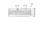
- FIG. 1 is a schematic sectional view showing a superconducting wire according to the first embodiment of the present invention.
- the superconducting wire 1A of the present embodiment is configured by laminating a bed layer 15, an intermediate layer 16, and a superconducting layer 17 on a tape-like base material 11.
- a metal stabilizing base layer 18 and a metal stabilizing layer 19 are laminated on the superconducting layer 17.
- a storage groove 9 is provided in the upper part (upper layer part) of the metal stabilizing layer 19.
- the temperature detection medium 10 is stored in the storage groove 9.
- the base material 11 applicable to the superconducting wire 1A of the present embodiment can be used as a base material of a normal superconducting wire, has only to be high strength, and is preferably in the form of a tape in order to obtain a long cable. It is preferable that it is a base material which consists of a property metal. Examples thereof include various metal materials such as nickel alloys such as silver, platinum, stainless steel, copper and hastelloy, or a base material in which ceramics are arranged on these various metal materials. Among various heat resistant metals, nickel alloys are preferable.
- Hastelloy (trade name made by US Haynes Co., Ltd.) is suitable, and Hastelloy B, C, G, N, W, which have different amounts of components such as molybdenum, chromium, iron, cobalt, etc. Any type can be used.
- the thickness of the substrate 11 may be appropriately adjusted according to the purpose, and is usually 10 to 500 ⁇ m.
- the bed layer 15 has high heat resistance and is a layer for reducing interfacial reactivity, and is used for obtaining the orientation of a film disposed thereon.
- a bed layer 15 is arranged as necessary, and is made of, for example, yttria (Y 2 O 3 ), silicon nitride (Si 3 N 4 ), aluminum oxide (Al 2 O 3 , also referred to as “alumina”), or the like. Composed.
- the bed layer 15 is formed by a film forming method such as a sputtering method.
- the thickness of the bed layer 15 is, for example, 10 to 200 nm.
- the superconducting wire 1 ⁇ / b> A is not limited to the structure shown in FIG.
- the diffusion prevention layer is a layer formed for the purpose of preventing the diffusion of the constituent elements of the substrate 11 and is made of silicon nitride (Si 3 N 4 ), aluminum oxide (Al 2 O 3 ), rare earth metal oxide, or the like. Is done.
- the thickness of the diffusion preventing layer is, for example, 10 to 400 nm. Note that since the crystallinity of the diffusion preventing layer is not questioned, it may be formed by a film forming method such as a normal sputtering method.
- the intermediate layer 16 may have either a single layer structure or a multilayer structure, and is selected from materials biaxially oriented in order to control the crystal orientation of the superconducting layer 17 laminated thereon.
- preferred materials for the intermediate layer 16 include Gd 2 Zr 2 O 7 , MgO, ZrO 2 —Y 2 O 3 (YSZ), SrTiO 3 , CeO 2 , Y 2 O 3 , Al 2 O 3, Gd 2 O. 3 , metal oxides such as Zr 2 O 3 , Ho 2 O 3 and Nd 2 O 3 can be exemplified.
- the cap layer is preferably interposed between the intermediate layer 16 and the superconducting layer 17 without being limited to the structure shown in FIG. If the intermediate layer 16 is formed with a good crystal orientation (for example, a crystal orientation degree of 15 ° or less) by ion beam assisted deposition (IBAD method), the crystal orientation of the cap layer formed thereon is good. Value (for example, a crystal orientation degree of around 5 °). Thereby, since the crystal orientation of the superconducting layer 17 formed on the cap layer can be improved, the superconducting layer 17 can exhibit excellent superconducting characteristics.
- a good crystal orientation for example, a crystal orientation degree of 15 ° or less
- IBAD method ion beam assisted deposition
- the thickness of the intermediate layer 16 may be adjusted as appropriate according to the purpose, but can usually be in the range of 0.005 to 2 ⁇ m.
- the intermediate layer 16 is formed by physical vapor deposition such as sputtering, vacuum vapor deposition, laser vapor deposition, electron beam vapor deposition, ion beam assisted vapor deposition (hereinafter abbreviated as IBAD), chemical vapor deposition (CVD).
- IBAD ion beam assisted vapor deposition
- CVD chemical vapor deposition
- the metal oxide layer formed by the IBAD method is preferable in that the crystal orientation is high and the effect of controlling the crystal orientation of the superconducting layer 17 and the cap layer is high.
- the IBAD method is a method of orienting crystal axes by irradiating an ion beam at a predetermined angle with respect to an underlying vapor deposition surface during vapor deposition.
- an argon (Ar) ion beam is used as the ion beam.
- the intermediate layer 16 made of Gd 2 Zr 2 O 7 , MgO, or ZrO 2 —Y 2 O 3 (YSZ) reduces the value of ⁇ (FWHM: full width at half maximum), which is an index representing the degree of crystal orientation in the IBAD method. This is particularly preferable because it can be performed.
- the cap layer was formed through a process of epitaxially growing on the surface of the intermediate layer 16 and then grain growth (overgrowth) in the lateral direction (plane direction), and crystal grains were selectively grown in the in-plane direction.
- a layer is preferred.
- Such a cap layer has a higher in-plane orientation degree than the intermediate layer 16 made of the metal oxide layer.
- the material of the cap layer is not particularly limited as long as it is a material that can exhibit the above functions. Specific examples of preferable materials include CeO 2 , Y 2 O 3 , Al 2 O 3 , Gd 2 O 3 , Zr 2 O 3 , Ho 2 O 3 , Nd 2 O 3 and the like.
- the cap layer may include a Ce—M—O-based oxide in which part of Ce is substituted with another metal atom or metal ion.
- the CeO 2 layer can be formed by a PLD method (pulse laser deposition method), a sputtering method, or the like, but it is desirable to use the PLD method from the viewpoint of obtaining a high film formation rate.
- the substrate temperature is about 500 to 1000 ° C. and the pressure is about 0.6 to 100 Pa in an oxygen gas atmosphere.
- the film thickness of the CeO 2 layer may be 50 nm or more, but is preferably 100 nm or more, and more preferably 500 nm or more in order to obtain sufficient orientation. However, since the crystal orientation deteriorates if the film thickness is too thick, the film thickness is preferably 500 to 1000 nm.
- the superconducting layer 17 may be a known layer, and specifically, a layer made of a material made of REBa 2 Cu 3 O y (RE represents a rare earth element such as Y, La, Nd, Sm, Er, Gd) can be exemplified. .
- RE represents a rare earth element such as Y, La, Nd, Sm, Er, Gd
- Examples of the superconducting layer 17 include Y123 (YBa 2 Cu 3 O 7-X ) or Gd123 (GdBa 2 Cu 3 O 7-X ).
- other oxide superconductors for example, Bi 2 Sr 2 Ca n- 1 Cu n O 4 + 2n + in ⁇ a composition or the like may be used a layer formed of other high oxide superconductor critical temperature represented.
- the thickness of the superconducting layer 17 is about 0.5 to 5 ⁇ m and is preferably a uniform thickness.
- the superconducting layer 17 can be laminated by a physical vapor deposition method such as sputtering, vacuum vapor deposition, laser vapor deposition, electron beam vapor deposition, chemical vapor deposition (CVD), coating thermal decomposition (MOD), or the like.
- a physical vapor deposition method such as sputtering, vacuum vapor deposition, laser vapor deposition, electron beam vapor deposition, chemical vapor deposition (CVD), coating thermal decomposition (MOD), or the like.
- a physical vapor deposition method such as sputtering, vacuum vapor deposition, laser vapor deposition, electron beam vapor deposition, chemical vapor deposition (CVD), coating thermal decomposition (MOD), or the like.
- TFA-MOD method organic metal deposition method using trifluoroacetate salt, coating pyrolysis method
- PLD method or CVD method
- the superconducting layer 17 laminated on the cap layer is also crystallized so as to match the orientation of the cap layer. . Therefore, the superconducting layer 17 formed on the cap layer has almost no disorder in the crystal orientation.
- the c-axis in which electricity is difficult to flow is oriented in the thickness direction of the base material 11, and the a-axis or b-axis is in the length direction of the base material 11.
- the obtained superconducting layer 17 is excellent in quantum connectivity at the crystal grain boundary, and there is almost no deterioration of the superconducting characteristics at the crystal grain boundary. Therefore, it becomes easy to flow electricity in the length direction of the base material 11, and a sufficiently high critical current density is obtained.
- the metal stabilizing base layer 18 laminated on the superconducting layer 17 is formed as a layer made of a metal material having good conductivity, such as Ag, and a low contact resistance with the superconducting layer 17.
- the thickness of the metal stabilizing base layer 18 is preferably 1 to 30 ⁇ m.
- the metal stabilizing base layer 18 can be formed by a known method. In particular, it is preferable to form by sputtering.
- the metal stabilizing layer 19 is made of a highly conductive metal material, and when the superconducting layer 17 attempts to transition from the superconducting state to the normal conducting state, the current of the superconducting layer 17 commutates together with the metal stabilizing base layer 18. Acts as a bypass.
- the metal material constituting the metal stabilizing layer 19 is not particularly limited as long as it is a material having good conductivity, but is relatively inexpensive such as copper, brass (Cu—Zn alloy), copper alloy, stainless steel, or the like. A material is preferably used, and copper is more preferable because it has high conductivity and is inexpensive.
- the thickness of the metal stabilizing layer 19 is preferably 10 to 300 ⁇ m. By setting the thickness to be equal to or greater than the lower limit value, a higher effect of stabilizing the superconducting layer 17 can be obtained.
- Superconducting wire 1A can be made thin by setting the thickness to the upper limit value or less.
- the metal stabilization layer 19 can be formed by a known method, and can be formed by a sputtering method or a method of soldering a metal tape such as copper onto the metal stabilization base layer 18.
- the temperature detection medium 10 is a medium that can detect a temperature change, and an optical fiber whose internal optical propagation state changes depending on the temperature, or a high resistance metal wire whose voltage value changes depending on the temperature (for example, , Carbon resistance, semiconductor) and the like can be used. Among them, it is preferable to use an optical fiber because temperature changes can be detected continuously with high accuracy and responsiveness. In addition, it is preferable to use an optical fiber as the temperature detection medium 10 because the diameter of the superconducting wire 1A can be reduced because the diameter of the optical fiber is generally thin.
- the shape of the temperature detection medium 10 is a long line. The diameter of the temperature detection medium 10 is several tens to 125 ⁇ m.
- an optical fiber generally used for temperature detection can be used.
- the temperature detection method of the optical fiber may be any of a wavelength multiplexing method, a time division multiplexing method, an FBG (Fiber BraggGrating) method, a BOCDA (Brillouin Optical Correlation Domain Analysis) method, and a Raman scattered light method.
- the outer peripheral part of the optical fiber may be covered with a coating material such as polyimide, or may not be covered.
- the thickness of the coating material is preferably 15 ⁇ m or less.
- the storage groove 9 is continuously formed along the longitudinal direction of the superconducting wire 1A.
- the temperature detection medium 10 is stored in the storage groove 9 along the longitudinal direction of the superconducting wire 1A.
- the storage groove 9 may be formed by processing with a laser or the like after the metal stabilizing layer 19 is laminated on the metal stabilizing base layer 18.
- the metal stabilization layer 19 may be laminated after the storage groove 9 is previously formed on the metal tape by a conventionally known method. .
- the temperature detection medium 10 is installed in the storage groove 9 by setting the width of the storage groove 9 in the short direction of the superconducting wire 1A to be approximately equal to or slightly larger than the diameter of the temperature detection medium 10. For example, a method of fitting 10 into the storage groove 9 or bonding with an adhesive may be used. In addition, when joining the temperature detection medium 10 to the storage groove 9 using an adhesive agent, the temperature detection medium 10 and the storage groove 9 (that is, the metal stabilization layer 19) are used so as not to cause a decrease in temperature change detection accuracy. It is preferable to make the region where the adhesive is interposed between the two as small as possible.
- a method of providing an adhesive so as to close only the upper portion of the temperature detection medium 10 and close the opening of the storage groove 9, or the upper surface of the temperature detection medium 10 and the opening of the storage groove 9 There is a method of providing an adhesive so as to block only a part of the gap.
- the method of fitting the temperature detection medium 10 into the storage groove 9 is simple, and the contact between the temperature detection medium 10 and the storage groove 9 (that is, the metal stabilization layer 19). This is preferable because the area increases and the temperature change detection accuracy is improved.
- the depth of the storage groove 9 can be appropriately adjusted according to the diameter of the temperature detection medium 10.
- the diameter of the temperature detection medium 10 is d and the depth of the storage groove 9 is L, it is preferable that d ⁇ L.
- a part of the temperature detection medium 10 may protrude from the upper surface of the metal stabilization layer 19.
- the structure in which d ⁇ L and the temperature detection medium 10 is disposed inside the metal stabilization layer 19 as described above increases the contact area between the temperature detection medium 10 and the metal stabilization layer 19.
- the superconducting wire 1A can be made thinner.
- the superconducting wire 1A when the superconducting wire 1A is wound concentrically to form a superconducting coil, the superconducting wire 1A can be wound at a high density, and a good current density can be obtained.
- the cross-sectional shape of the storage groove 9 is a rectangle is illustrated, this embodiment is not limited only to this example.
- the bottom shape of the storage groove 9 is formed in an arc shape or the like in accordance with the cross-sectional shape of the temperature detection medium 10 (circular in FIG. 1).
- the contact area with the stabilization layer 19 can be increased to improve the temperature change detection accuracy, and the joint structure by fitting the storage groove 9 and the temperature detection medium 10 can be further strengthened.
- the superconducting wire 1A may employ a configuration in which the exposed surface around the superconducting wire 1A is covered with an insulating insulating layer 20.
- the insulating layer 20 is a layer made of a known material such as various resins and oxides that are usually used. Specific examples of the resin include polyimide resin, polyamide resin, epoxy resin, acrylic resin, phenol resin, melamine resin, polyester resin, silicon resin, silicon resin, alkyd resin, and vinyl resin.
- the thickness of the coating by the insulating layer 20 is not particularly limited, and may be appropriately adjusted according to the portion to be coated.
- the insulating layer 20 may be formed by a known method depending on the material, for example, a raw material may be applied and cured. If a sheet-like material is available, it may be used for coating.
- the metal stabilizing base layer 18 and the metal stabilizing layer 19 are provided with the superconducting layer 17.
- Current commutates.
- the temperature detection medium 10 is disposed near the superconducting layer 17 and in the storage groove 9 formed in the metal stabilizing layer 19 even if a normal conducting transition occurs.
- the temperature change (temperature rise) inside the superconducting wire 1A can be detected with good accuracy and responsiveness.
- the superconducting wire 1A of the present embodiment is arranged not inside the insulating layer 20 but inside the metal stabilizing layer 19, so that detection due to noise caused by the insulating layer 20 is detected. This is preferable because accuracy does not deteriorate.
- the superconducting wire 1A of the present embodiment can be made thinner than the case where the temperature detection medium is installed on the outer peripheral surface of the superconducting wire, and the superconducting wire 1A is wound concentrically to form a superconducting coil.
- the superconducting wire 1A can be wound at a high density, and the current density can be improved.
- a configuration in which one temperature detection medium 10 is arranged inside the metal stabilization layer 19 is illustrated.
- the present invention is not limited to this configuration, and in order to improve the reliability of the superconducting wire 1 ⁇ / b> A, two or more temperature detection media 10 may be arranged inside the metal stabilization layer 19. it can.
- FIG. 2 is a schematic sectional view showing a superconducting wire according to the second embodiment of the present invention.
- the superconducting wire 2A of the present embodiment includes a laminated body S1 in which a bed layer 15, an intermediate layer 16, a superconducting layer 17, and a metal stabilizing base layer 18 are laminated in this order on a tape-like base material 11, and this laminated body.
- Metal stabilization layers 19a, 19b, 19c and 19d (metal stabilization layer 19) formed so as to cover the upper surface, one side surface, the other side surface and the lower surface of S1, respectively, and the metal stabilization layer on laminate S1 In 19a, it is roughly comprised by the temperature detection medium 10 distribute
- the superconducting wire 2A of the second embodiment is the same as that of the first embodiment described above in that the metal stabilizing layer 19 is provided around the laminate S1 and that the temperature detection medium 10 is in contact with the metal stabilizing base layer 18. This is different from the superconducting wire 1A.
- the metal stabilization layers 19a, 19b, 19c, and 19d are made of a highly conductive metal material, and the metal stabilization is performed when the superconducting layer 17 attempts to transition from the superconducting state to the normal conducting state. Together with the base layer 18, it functions as a bypass through which the current of the superconducting layer 17 commutates.
- the metal material constituting the metal stabilization layers 19a to 19d may be any material having good conductivity, and is not particularly limited. However, a relatively inexpensive material such as copper may be used. preferable.
- the thickness of the metal stabilization layers 19a to 19d is preferably 10 to 300 ⁇ m. By setting the thickness to be equal to or greater than the lower limit value, a higher effect of stabilizing the superconducting layer 17 can be obtained.
- Superconducting wire 2A can be made thin by setting the thickness to the upper limit value or less.
- the metal stabilizing layers 19a to 19d are formed by a plating method.
- the temperature detection medium 10 is arranged in the metal stabilization layer 19 on the metal stabilization base layer 18 so that the upper surface of the metal stabilization base layer 18 and the lower surface of the temperature detection medium 10 are in contact with each other.
- a laminate S1 of the base material 11, the bed layer 15, the intermediate layer 16, the superconducting layer 17, and the metal stabilization base layer 18 was formed.
- metal stabilizing layers 19a to 19d are formed by plating a highly conductive metal such as copper with the temperature detection medium 10 placed along the upper surface of the laminate S1 (the upper surface of the metal stabilizing base layer 18).
- a highly conductive metal such as copper
- the superconducting wire 2A if a normal conducting transition occurs, the current of the superconducting layer 17 is commutated in the metal stabilizing base layer 18 and the metal stabilizing layer 19, and heat is generated due to Joule heat.
- the superconducting wire 2A according to the present embodiment has the above-described configuration in which the lower surface of the temperature detection medium 10 is disposed in the metal stabilization layer 19a in a state of being in contact with the upper surface of the metal stabilization base layer 18 laminated on the superconducting layer 17.
- the detection accuracy and responsiveness of temperature change (temperature rise) inside the wire can be further improved.
- the thickness of the metal stabilization layer 19a is substantially the same as the diameter of the temperature detection medium 10.
- the present embodiment is not limited only to this configuration.
- the thickness of the metal stabilization layer 19a may be set larger than the diameter of the temperature detection medium 10, and the temperature detection medium 10 may be completely buried in the metal stabilization layer 19a.
- the temperature detection medium 10 and the insulating layer do not come into contact with each other when the periphery is covered with the insulating layer. For this reason, the noise resulting from an insulating layer does not generate
- a configuration in which one temperature detection medium 10 is arranged inside the metal stabilization layer 19a is illustrated.
- the present invention is not limited only to this configuration.
- a configuration in which two or more temperature detection media 10 are arranged inside the metal stabilization layer 19a may be employed.
- FIG. 3 is a schematic sectional view showing a superconducting wire according to the third embodiment of the present invention.
- the superconducting wire 3A of the present embodiment includes a laminated body S1 in which a bed layer 15, an intermediate layer 16, a superconducting layer 17, and a metal stabilizing base layer 18 are laminated in this order on a tape-shaped substrate 11, and this laminated body.
- Metal stabilization layers 19a, 19b, 19c and 19d (metal stabilization layer 19) formed so as to cover the upper surface, one side surface, the other side surface and the lower surface of S1, respectively, and the metal stability on the side of superconducting layer 17 And a temperature detection medium 10 disposed in the conversion layer 19b.
- the superconducting wire 3A of the third embodiment is different from the superconducting wire 2A of the second embodiment described above in that the temperature detection medium 10 is disposed in the metal stabilization layer 19b.
- the same layers as in the second embodiment can be cited, and they are formed by a plating method.
- a method of installing the temperature detection medium 10 in the metal stabilization layer 19b by plating a highly conductive metal such as copper with the temperature detection medium 10 placed along one side surface of the laminate S1, There is a method in which the temperature detection medium 10 is buried and fixed in the metal stabilization layer 19b at the same time as the metal stabilization layers 19a to 19d are formed.
- the temperature detection medium 10 is disposed in the metal stabilization layer 19b in contact with the side surface of the superconducting layer 17. For this reason, in the unlikely event that a normal conduction transition occurs, it is possible to detect heat generation due to current flowing from the superconducting layer 17 to the metal stabilizing layer 19b with good accuracy and responsiveness. Furthermore, by providing the temperature detection medium 10 at a position close to the superconducting layer 17 in the metal stabilization layer 19b, the temperature detection accuracy and responsiveness can be further improved.
- FIG. 3 illustrates the case where the thickness of the metal stabilizing layer 19b is substantially the same as the diameter of the temperature detection medium 10.
- the present embodiment is not limited only to this configuration.
- the thickness of the metal stabilization layer 19b may be set larger than the diameter of the temperature detection medium 10, and the temperature detection medium 10 may be completely buried in the metal stabilization layer 19b.
- the temperature detection medium 10 and the insulating layer are not in contact with each other even when the periphery is covered with the insulating layer. Does not occur, and the detection accuracy can be improved.
- arranged inside the metal stabilization layer 19b was illustrated.
- the present invention is not limited only to this configuration.
- a configuration including two or more temperature detection media 10 may be employed.
- the arrangement of the plurality of temperature detection media 10 is not particularly limited, and a plurality of temperature detection media 10 may be arranged in the metal stabilization layer 19b, or a laminate.
- the metal stabilization layer 19b on one side surface of S1 and the metal stabilization layer 19c on the other side surface of the stacked body S1 may be disposed.
- the temperature detection medium 10 may be arranged. Further, the temperature detection medium 10 may be arranged on the metal stabilization layer 19a on the multilayer body S1 and the metal stabilization layers 19b and 19c on both side surfaces of the multilayer body S1, respectively.
- the number of temperature detection media 10 per superconducting wire is not particularly limited.
- FIG. 5 is a schematic cross-sectional view showing a superconducting wire according to another embodiment of the present invention.
- the superconducting wire 4A of this embodiment is a wire having a flat cross-sectional shape and covers the periphery of the superconducting layer 37 having a flat cross-sectional shape formed by a plurality of superconductor filaments extending in the longitudinal direction.
- the flat metal stabilization layer 39 and the temperature detection medium 10 accommodated in the accommodation groove 9 formed in the metal stabilization layer 39 are schematically configured.
- Bi 2 Sr 2 Ca 1 Cu 2 O x (Bi 2212 phase), Bi 2 Sr 2 Ca 2 Cu 3 O y (Bi 2223 phase), Bi 1.6 Pb 0.4
- High-temperature superconducting materials such as oxide superconducting materials having compositions represented by Sr 2 Ca 2 Cu 3 O x , Tl 2 Ba 2 Ca 2 Cu 3 O y , Y 1 Ba 2 Cu 3 O 7-x , and Nb
- oxide superconducting materials having compositions represented by Sr 2 Ca 2 Cu 3 O x , Tl 2 Ba 2 Ca 2 Cu 3 O y , Y 1 Ba 2 Cu 3 O 7-x , and Nb
- One or more materials selected from low-temperature superconducting materials having a composition represented by 3 Sn, Nb 3 Al, or the like are used.
- Bi2223 phase or Bi2212 phase Bi-based oxide superconducting materials are used.
- the metal stabilization layer 39 is made of silver or a silver alloy.
- the metal stabilizing layer 39 may be made of copper or a copper alloy.
- the storage groove 9 and the temperature detection medium 10 can have the same configuration and structure as those of the first embodiment described above.
- the superconducting wire 4A of this embodiment is a PIT method (Powder In Tube) in which a silver or silver alloy pipe filled with the raw material powder of the superconducting layer 37 is drawn to form a multi-core, and the wire drawing, rolling and firing are repeated. Method).
- the thickness of the superconducting wire 4A is about 0.2 to 0.3 mm in the case of a tape-shaped conductor structure.
- the volume ratio between the superconducting layer 37 and the metal stabilizing layer 39 can be set to about 2: 3, for example.
- the metal stabilizing layer 39 covers the entire circumference of the superconducting layer 37.
- the storage groove 9 is continuously formed in the upper part of the protruding portion 39a on one end side in the width direction of the superconducting layer 37 along the longitudinal direction of the superconducting wire 4A.
- the temperature detection medium 10 is stored in the storage groove 9 along the longitudinal direction of the superconducting wire 4A.
- the storage groove 9 is formed by, for example, processing the metal stabilization layer 19 with a laser or the like after the superconducting layer 37 and the metal stabilization layer 39 are formed by wire drawing, rolling and firing, or roll rolling. Sometimes, it can be performed by forming a groove by roll rolling in the protruding portion 39a where there is no superconducting layer 37.
- the method of installing the temperature detection medium 10 in the storage groove 9 is the same as that in the first embodiment.
- the temperature detection medium 10 is arranged on the metal stabilization layer 39, similarly to the superconducting wires of the first to third embodiments. That is, when the metal stabilization layer 39 is formed of copper or a copper alloy, the temperature detection medium 10 is disposed on the copper layer or the copper alloy layer. Further, when the metal stabilizing layer 39 is made of silver or a silver alloy, the temperature detection medium 10 may be disposed on the silver layer or the silver alloy layer. Thereby, even if a normal conduction transition occurs, a temperature change (temperature rise) inside the superconducting wire 4A can be detected with good accuracy and responsiveness.
- the superconducting wire 4A of the present embodiment can be made thinner than when the temperature detection medium is installed on the outer peripheral surface of the superconducting wire. Therefore, when the superconducting wire 4A is wound concentrically to form a superconducting coil, the superconducting wire 4A can be wound at a high density, and the current density can be improved.
- a configuration in which one temperature detection medium 10 is arranged inside the metal stabilization layer 39 is illustrated.
- the present invention is not limited to this configuration, and in order to improve the reliability of the superconducting wire 4A, two or more temperature detection media 10 may be arranged inside the metal stabilization layer 39. it can.
- the arrangement of the temperature detection medium 10 in the metal stabilization layer 39 can be changed as appropriate.
- the example in which the superconducting layer 37 is formed by a plurality of superconducting filaments has been shown.
- the present embodiment is not limited to this configuration, and the superconducting layer 37 may be formed of a single superconducting filament.
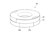
- FIG. 7 is a schematic perspective view showing a superconducting coil 50 according to an embodiment of the present invention.
- the superconducting coil 50 is configured by coaxially laminating a second coil body 52 on a first coil body 51.
- the first coil body 51 is a pancake-type coil body configured by winding the superconducting wire of the present embodiment described above many times in a concentric and counterclockwise manner.
- the second coil body 52 is a pancake-type coil body that is formed by winding the superconducting wire of the present embodiment described above concentrically and many times clockwise.
- the outer peripheral end 51a which is the winding end of the first coil body 51
- the outer peripheral end 52a which is the winding end of the second coil body 52
- the temperature detection medium provided in each superconducting wire constituting the first coil body 51 and the second coil body 52 can detect a temperature change (temperature rise) in the superconducting coil 50. If so, it may be arranged independently in each coil body, or may be continuously arranged in two coil bodies.
- the superconducting coil 50 of this embodiment includes a coil body formed by winding the superconducting wire of this embodiment. Thereby, even if a normal conducting transition occurs, an internal temperature change (temperature rise) can be detected with good accuracy and responsiveness. Further, the superconducting coil 50 of the present embodiment is formed of the superconducting wire of the present embodiment having a configuration in which the temperature detection medium is embedded in the metal stabilizing layer of the superconducting wire. With this configuration, since the superconducting wire can be wound at a high density, the current density can be improved.
- the superconducting coil 50 having a configuration in which two coil bodies are stacked is illustrated.
- This invention is not limited only to this structure, You may be formed from 3 or more coil bodies.
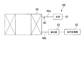
- FIG. 8 is a schematic configuration diagram showing a superconducting protection device 100 according to an embodiment of the present invention.
- the superconducting protection device 100 one end 60 a of the optical fiber 60 that is a temperature detection unit provided in the superconducting coil 50 of the present embodiment is communicated with the light source 61, and the other end 60 b of the optical fiber 60 is signal-processed via the detector 62. It is communicated with the vessel 63 and is schematically configured.
- the superconducting protection device 100 operates the light source 61 so that light enters the optical fiber 60 from one end 60 a of the optical fiber 60, and the detector 62 and the signal processor 63 cause superconductivity at the other end 60 b of the optical fiber 60.
- the light propagating through the coil 50 is detected.
- a superconducting transition occurs in the superconducting coil 50, a change appears in a signal that is immediately detected due to a temperature change inside the superconducting coil 50, so that the normal conducting transition can be detected.
- the case where the temperature detection unit is the optical fiber 60 is illustrated.
- the detector and the signal processing device may be configured to communicate with the end of the temperature detection unit extending from the superconducting coil.
- the superconducting protection device 100 of the present embodiment includes the superconducting coil 50 of the present embodiment. Therefore, even if a normal conducting transition occurs, an internal temperature change (temperature rise) can be detected with good accuracy and responsiveness. Therefore, in the unlikely event that the normal conduction transition occurs, it is possible to prevent the superconducting coil 50 from being burned out by reducing the current value, and to protect the superconducting coil 50 in a good state.
- each part of the superconducting wire, each part that constitutes the superconducting coil, and each part that constitutes the superconducting protection device are examples.
- the present invention can be changed as appropriate without departing from the scope of the present invention.
- GdBa 2 Cu 3 O 7 (superconducting layer) having a thickness of 1.0 ⁇ m was formed on the CeO 2 layer by the PLD method. Further, a 10 ⁇ m silver layer (metal stabilizing base layer) was formed on the superconducting layer by sputtering. Thereafter, a copper layer (metal stabilization layer) having a thickness of 0.1 mm was laminated on the silver layer with solder. Further, a storage groove having a depth of 80 ⁇ m and a width of 80 ⁇ m was processed on the upper surface of the copper layer by a laser. An optical fiber having an outer diameter of 80 ⁇ m was accommodated in the accommodation groove to produce a superconducting wire having the structure shown in FIG.
- the winding tapes were wound so that the end portions in the width direction did not overlap each other.
- the thickness of the superconducting wire after winding the polyimide tape was about 0.25 mm.
- the obtained superconducting wire with polyimide tape was wound 35 times concentrically with an inner diameter of 70 mm to produce a coil body.
- 12 coil bodies produced in the same procedure were laminated on the same axis to produce a superconducting coil having a height of 72 mm and a total number of turns of 420 (35 turns ⁇ 12).
- Example 1 and Example 2 which are the superconducting coils of this embodiment, the central magnetic field for the same energizing current is stronger and the current density is higher than in Comparative Example 1 and Comparative Example 2. It was confirmed to be high.
- the superconducting coil of the example is thinner than the superconducting wire of the comparative example due to the configuration in which the optical fiber is arranged inside the metal stabilization layer, so the outer diameter of the coil is smaller than the superconducting coil of the comparative example.
- the wire length used is also small.
- the superconducting wire of the comparative example is provided with an optical fiber on the upper surface of the superconducting wire, in the coil body in which the superconducting wire is wound, the optical fiber is interposed between the superconducting wires adjacent in the radial direction. Exists. For this reason, the distance between each superconducting wire has increased. For this reason, the outer diameter of the superconducting coil of the comparative example was increased, and the length of the wire used was also increased. In addition, since the distance between each superconducting wire is increased, the current density of the coil is also reduced, and the central magnetic field is weakened.
- the present invention can provide a superconducting wire that can detect a temperature change inside the wire with good accuracy and responsiveness, and can also make the wire itself thin. Further, the present invention can provide a superconducting coil and a superconducting protection device that can detect an internal temperature change with good accuracy and responsiveness without reducing the current density.
Landscapes
- Physics & Mathematics (AREA)
- Electromagnetism (AREA)
- Engineering & Computer Science (AREA)
- Power Engineering (AREA)
- Superconductors And Manufacturing Methods Therefor (AREA)
Abstract
この超電導線材は、超電導層と;金属安定化層と;少なくともその一部が前記金属安定化層の内部に配されている温度検知媒体と;を備える。
Description
本発明は、超電導線材、超電導コイル、及び超電保護装置に関する。
本願は、2010年4月12日に、日本に出願された特願2010-091358号に基づき優先権を主張し、その内容をここに援用する。
本願は、2010年4月12日に、日本に出願された特願2010-091358号に基づき優先権を主張し、その内容をここに援用する。
NbTi等の合金系超電導体やNb3Sn等の化合物系超電導体などの金属系の低温超電導体を使用した低温超電導コイルは、超電導体の臨界温度が10K以下と低いため、運転温度は4K程度と極低温であり、比熱が小さい。そのため、低温超電導コイルにおいて何らかの原因で超電導状態から常電導状態へ遷移する常電導転移が発生すると、ジュール熱が発生して超電導コイルの温度が上昇する。これにより、臨界電流が低下して発熱し、超電導コイルの温度がさらに上昇する。このような発熱と温度上昇が繰り返されると、急激な常電導転移が発生して、超電導コイルの常電導領域が拡大してしまい、超電導特性の低下やコイルの損傷につながる可能性がある。そのため、超電導コイルにおける常電導転移の発生を確実かつ速やかに検出して常電導領域の拡大を防ぐことが重要である。金属系の低温超電導体を使用した低温超電導コイルにおける常電導転移の検出手法としては、常電導転移により発生した電圧を検知する方法や、バランス電圧を検知する方法が知られている。
しかし、Bi系やY系に代表されるような酸化物超電導体は、臨界温度が100K程度の高温超電導体であるため、運転温度は20K以上が想定される。金属系の低温超電導体と比較すると、運転温度での比熱が大きく、常電導転移した際の伝搬速度が遅い。そのため、従来の電圧測定による検出法では、常電導転移の発生を上手く検出できない可能性がある。
電圧測定による検出法ではなく、電磁的にノイズに強い常電導転移検出法として、温度に依存して内部の光学的伝播状態が変化する光ファイバを使用した手法が提案されている(下記特許文献1参照)。また、常電導転移検出法ではないが、光ファイバの外周面上に超電導体層が形成され、光ファイバと超電導体層とが同心円構造で複合された線材も提案されている(下記特許文献2参照)。
電圧測定による検出法ではなく、電磁的にノイズに強い常電導転移検出法として、温度に依存して内部の光学的伝播状態が変化する光ファイバを使用した手法が提案されている(下記特許文献1参照)。また、常電導転移検出法ではないが、光ファイバの外周面上に超電導体層が形成され、光ファイバと超電導体層とが同心円構造で複合された線材も提案されている(下記特許文献2参照)。
上記特許文献1では、2つのコアを有した光ファイバを伝搬するレーザ光で干渉系を組み、レーザ光の位相変化により10K程度の温度上昇を検出する方法が提案されている。しかしながら、この検出方法では、温度上昇の光ファイバ加熱長が2~6mと長く、大型の超電導コイルには適用可能であるが、数cm程度の微小な区間の温度上昇を検知することは困難であると考えられる。
また、上記特許文献2では、光ファイバの外周面上に超電導体層が被覆形成された線材が提案されている。しかしながら、Y系酸化物超電導線材においては、超電導体層の結晶を配向させるための中間層などの形成が必要不可欠である。このため、上記特許文献2に記載されるように光ファイバの外周面上に直接超電導体層を形成することは、Y系酸化物超電導線材では実現の可能性が極めて低いと考えられる。
また、上記特許文献2では、光ファイバの外周面上に超電導体層が被覆形成された線材が提案されている。しかしながら、Y系酸化物超電導線材においては、超電導体層の結晶を配向させるための中間層などの形成が必要不可欠である。このため、上記特許文献2に記載されるように光ファイバの外周面上に直接超電導体層を形成することは、Y系酸化物超電導線材では実現の可能性が極めて低いと考えられる。
光ファイバを用いた温度検知の手法では、超電導線材の温度上昇と共に、光ファイバに速やかに温度上昇が伝わる必要がある。BOCDA(Brillouin Optical Correlation Domain Analysis)方式やFBG(Fiber Bragg Grating)方式などの光ファイバでは、光ファイバの温度変化によって、光ファイバおよび光ファイバ被覆材に歪が生じる。その歪によって、光ファイバ内を伝送する光が多くの散乱を受けたり、反射光の波長が変化したりすることを利用して温度変化の検知を行う。
一般的に、超電導コイルは、低温超電導体、高温超電導体に限らず、超電導線材の他に、超電導線材の上部や周面部に含浸材や補強材などが形成されて構成されている。このような構造の超電導線材を用いて超電導コイル内に光ファイバを設置する場合、光ファイバを超電導線材の含浸材や補強材などの上面や内部に設置する方法や、超電導コイルの外面に設置する方法が考えられる。しかしながら、このような設置方法では、超電導線材で発生した熱が光ファイバに十分に伝熱しないばかりではなく、含浸材や補強材と接しているためにノイズが発生し、光ファイバの分解能が落ちてしまう可能性がある。また、含浸材や補強材の上面に光ファイバを設置した場合や、含浸材の厚さよりもその径が大きい光ファイバを含浸材内部にその一部が埋没されるように設置した場合、このような超電導線材を用いた超電導コイルでは、その径方向に隣接する各超電導線材間に光ファイバが存在するため、超電導線材を巻線する密度が粗くなってしまう。そのため、電流密度が下がるので超電導コイルが発生する磁場が低下し、超電導性能が低下してしまうことが考えられる。
本発明は、このような従来の実情に鑑みてなされたものであり、線材内部の温度変化を良好な精度および応答性で検知可能であり、且つ、線材自体を薄くすることも可能な超電導線材の提供を目的とする。また、本発明は、電流密度を低下させること無く、内部の温度変化を良好な精度および応答性で検知可能な超電導コイル、及び超電導保護装置の提供を目的とする。
上記課題を解決するため、本発明は以下の構成を採用した。
本発明の一態様に係る超電導線材は、超電導層と;金属安定化層と;少なくともその一部が前記金属安定化層の内部に配されている温度検知媒体と;を備える。
前記温度検知媒体が、光ファイバであってもよい。
前記温度検知媒体が、前記金属安定化層の内部の上層部に配されていてもよい。
前記超電導層と前記金属安定化層との間に介在された金属安定化基層を有し、前記温度検知媒体が、前記金属安定化基層に接触するように配されている構成を採用してもよい。
前記金属安定化層が、前記超電導層の上部及び側部に配され、前記温度検知媒体が、前記超電導層の側方に配されている構成を採用してもよい。
前記温度検知媒体を、少なくとも2つ備えていてもよい。
本発明の別の態様に係る超電導コイルは、上記超電導線材を備える。
本発明のさらに別の態様に係る超電導保護装置は、上記超電導コイルを備える。
本発明の一態様に係る超電導線材は、超電導層と;金属安定化層と;少なくともその一部が前記金属安定化層の内部に配されている温度検知媒体と;を備える。
前記温度検知媒体が、光ファイバであってもよい。
前記温度検知媒体が、前記金属安定化層の内部の上層部に配されていてもよい。
前記超電導層と前記金属安定化層との間に介在された金属安定化基層を有し、前記温度検知媒体が、前記金属安定化基層に接触するように配されている構成を採用してもよい。
前記金属安定化層が、前記超電導層の上部及び側部に配され、前記温度検知媒体が、前記超電導層の側方に配されている構成を採用してもよい。
前記温度検知媒体を、少なくとも2つ備えていてもよい。
本発明の別の態様に係る超電導コイルは、上記超電導線材を備える。
本発明のさらに別の態様に係る超電導保護装置は、上記超電導コイルを備える。
上記本発明の一態様に係る超電導線材によれば、超電導層に近い金属安定化層に温度検知媒体が配されている構成により、万一、常電導転移が発生した場合にも、良好な精度および応答性で、線材内部の温度変化(温度上昇)を検知できる。
上記本発明の一態様に係る超電導線材によれば、温度検知媒体の少なくとも一部が金属安定化層の内部に配されている構成により、温度検知媒体を超電導線材の外周面に設置する場合と比較して、線材自体を薄くできる。また、超電導線材を同心円状に巻回して超電導コイルとする場合、超電導線材を高密度で巻回でき、電流密度を良好にできる。
上記本発明の一態様に係る超電導線材によれば、温度検知媒体が超電導層上の金属安定化基層に接する状態で金属安定化層内に配されている構成により、より一層内部の温度変化(温度上昇)の検知精度および応答性を向上できる。
上記本発明の一態様に係る超電導線材によれば、超電導層の側面と接する金属安定化層内に温度検知媒体が配される構成により、万一、常電導転移が発生した場合、超電導層より金属安定化層へと電流が転流することによる発熱を、より一層良好な精度および応答性で検知できる。
上記本発明の一態様に係る超電導線材によれば、温度検知媒体の少なくとも一部が金属安定化層の内部に配されている構成により、温度検知媒体を超電導線材の外周面に設置する場合と比較して、線材自体を薄くできる。また、超電導線材を同心円状に巻回して超電導コイルとする場合、超電導線材を高密度で巻回でき、電流密度を良好にできる。
上記本発明の一態様に係る超電導線材によれば、温度検知媒体が超電導層上の金属安定化基層に接する状態で金属安定化層内に配されている構成により、より一層内部の温度変化(温度上昇)の検知精度および応答性を向上できる。
上記本発明の一態様に係る超電導線材によれば、超電導層の側面と接する金属安定化層内に温度検知媒体が配される構成により、万一、常電導転移が発生した場合、超電導層より金属安定化層へと電流が転流することによる発熱を、より一層良好な精度および応答性で検知できる。
上記本発明の別の態様に係る超電導コイルによれば、上記本発明の一態様に係る超電導線材を巻回して形成されたコイル体を備える構成により、万一、常電導転移が発生した場合にも、良好な精度および応答性で、内部の温度変化(温度上昇)を検知できる。
上記本発明の別の態様に係る超電導コイルによれば、温度検知媒体の少なくとも一部が、超電導線材の金属安定化層の内部に埋め込まれている構成である上記本発明の一態様に係る超電導線材を用いる構成により、超電導線材を高密度で巻回できるので、電流密度を良好にできる。
上記本発明のさらに別の態様に係る超電導保護装置は、上記本発明の別の態様に係る超電導コイルを備える構成により、万一、常電導転移が発生した場合にも、良好な精度および応答性で、超電導コイル内部の温度変化(温度上昇)を検知できる。従って、万一、常電導転移が発生した場合、電流値を低下させるなどして超電導コイルの焼損につながることを防止し、超電導コイルを良好な状態で保護することができる。
上記本発明の別の態様に係る超電導コイルによれば、温度検知媒体の少なくとも一部が、超電導線材の金属安定化層の内部に埋め込まれている構成である上記本発明の一態様に係る超電導線材を用いる構成により、超電導線材を高密度で巻回できるので、電流密度を良好にできる。
上記本発明のさらに別の態様に係る超電導保護装置は、上記本発明の別の態様に係る超電導コイルを備える構成により、万一、常電導転移が発生した場合にも、良好な精度および応答性で、超電導コイル内部の温度変化(温度上昇)を検知できる。従って、万一、常電導転移が発生した場合、電流値を低下させるなどして超電導コイルの焼損につながることを防止し、超電導コイルを良好な状態で保護することができる。
[超電導線材]
<第1実施形態>
図1は、本発明の第1実施形態に係る超電導線材を示す概略断面図である。
本実施形態の超電導線材1Aは、テープ状の基材11の上にベッド層15と中間層16と超電導層17とが積層されて構成される。この超電導層17の上に、金属安定化基層18と金属安定化層19とが積層される。この金属安定化層19の上部(上層部)に、収納溝9が設けられる。この収納溝9に、温度検知媒体10が収容される。
<第1実施形態>
図1は、本発明の第1実施形態に係る超電導線材を示す概略断面図である。
本実施形態の超電導線材1Aは、テープ状の基材11の上にベッド層15と中間層16と超電導層17とが積層されて構成される。この超電導層17の上に、金属安定化基層18と金属安定化層19とが積層される。この金属安定化層19の上部(上層部)に、収納溝9が設けられる。この収納溝9に、温度検知媒体10が収容される。
本実施形態の超電導線材1Aに適用できる基材11は、通常の超電導線材の基材として使用でき、高強度であれば良く、長尺のケーブルとするためにテープ状であることが好ましく、耐熱性の金属からなる基材であることが好ましい。例えば、銀、白金、ステンレス鋼、銅、ハステロイ等のニッケル合金等の各種金属材料、もしくはこれら各種金属材料上にセラミックスを配した基材等が挙げられる。各種耐熱性の金属の中でも、ニッケル合金が好ましい。なかでも、市販品であれば、ハステロイ(米国ヘインズ社製商品名)が好適であり、ハステロイとして、モリブデン、クロム、鉄、コバルト等の成分量が異なる、ハステロイB、C、G、N、W等のいずれの種類も使用できる。基材11の厚さは、目的に応じて適宜調整すれば良く、通常は、10~500μmである。
ベッド層15は、耐熱性が高く、界面反応性を低減するための層であり、その上に配される膜の配向性を得るために用いる。このようなベッド層15は、必要に応じて配され、例えば、イットリア(Y2O3)、窒化ケイ素(Si3N4)、酸化アルミニウム(Al2O3、「アルミナ」とも呼ぶ)等から構成される。このベッド層15は、例えばスパッタリング法等の成膜法により形成される。ベッド層15の厚さは、例えば10~200nmである。
また、本発明において、超電導線材1Aは、図1に示す構造のみに限らず、基材11とベッド層15との間に拡散防止層が介在された構造を有しても良い。拡散防止層は、基材11の構成元素拡散を防止する目的で形成された層であり、窒化ケイ素(Si3N4)、酸化アルミニウム(Al2O3)、あるいは希土類金属酸化物等から構成される。拡散防止層の厚さは、例えば10~400nmである。なお、拡散防止層の結晶性は問われないので、通常のスパッタ法等の成膜法により形成すればよい。
このように基材11とベッド層15との間に拡散防止層を介在させることにより、後述する中間層16や超電導層17等の他の層を形成する際に、必然的に加熱されたり、熱処理される結果として熱履歴を受ける場合に、基材11の構成元素の一部がベッド層15を介して超電導層17側に拡散することを効果的に抑制できる。基材11とベッド層15との間に拡散防止層を介在させる場合の例としては、拡散防止層としてAl2O3を用い、ベッド層15としてY2O3を用いる組み合わせを例示できる。
また、本発明において、超電導線材1Aは、図1に示す構造のみに限らず、基材11とベッド層15との間に拡散防止層が介在された構造を有しても良い。拡散防止層は、基材11の構成元素拡散を防止する目的で形成された層であり、窒化ケイ素(Si3N4)、酸化アルミニウム(Al2O3)、あるいは希土類金属酸化物等から構成される。拡散防止層の厚さは、例えば10~400nmである。なお、拡散防止層の結晶性は問われないので、通常のスパッタ法等の成膜法により形成すればよい。
このように基材11とベッド層15との間に拡散防止層を介在させることにより、後述する中間層16や超電導層17等の他の層を形成する際に、必然的に加熱されたり、熱処理される結果として熱履歴を受ける場合に、基材11の構成元素の一部がベッド層15を介して超電導層17側に拡散することを効果的に抑制できる。基材11とベッド層15との間に拡散防止層を介在させる場合の例としては、拡散防止層としてAl2O3を用い、ベッド層15としてY2O3を用いる組み合わせを例示できる。
中間層16は、単層構造あるいは複層構造のいずれでも良く、その上に積層される超電導層17の結晶配向性を制御するために2軸配向する物質から選択される。中間層16の好ましい材質として具体的には、Gd2Zr2O7、MgO、ZrO2-Y2O3(YSZ)、SrTiO3、CeO2、Y2O3、Al2O3、Gd2O3、Zr2O3、Ho2O3、Nd2O3等の金属酸化物を例示できる。なお、本実施形態の超電導線材1Aにおいて、図1に示す構造のみに限定されず、中間層16と超電導層17との間にキャップ層が介在されていることが好ましい。
この中間層16をイオンビームアシスト蒸着法(IBAD法)により良好な結晶配向性(例えば結晶配向度15゜以下)で成膜するならば、その上に形成するキャップ層の結晶配向性を良好な値(例えば結晶配向度5゜前後)とすることができる。これにより、キャップ層の上に成膜する超電導層17の結晶配向性を良好にできるため、超電導層17が優れた超電導特性を発揮できる。
この中間層16をイオンビームアシスト蒸着法(IBAD法)により良好な結晶配向性(例えば結晶配向度15゜以下)で成膜するならば、その上に形成するキャップ層の結晶配向性を良好な値(例えば結晶配向度5゜前後)とすることができる。これにより、キャップ層の上に成膜する超電導層17の結晶配向性を良好にできるため、超電導層17が優れた超電導特性を発揮できる。
中間層16の厚さは、目的に応じて適宜調整すれば良いが、通常は、0.005~2μmの範囲とすることができる。
中間層16は、スパッタ法、真空蒸着法、レーザ蒸着法、電子ビーム蒸着法、イオンビームアシスト蒸着法(以下、IBAD法と略記する)、化学気相成長法(CVD法)等の物理的蒸着法;塗布熱分解法(MOD法);溶射等、酸化物薄膜を形成する公知の方法で積層できる。特に、IBAD法で形成された前記金属酸化物層は、結晶配向性が高く、超電導層17やキャップ層の結晶配向性を制御する効果が高い点で好ましい。IBAD法とは、蒸着時に、下地の蒸着面に対して所定の角度でイオンビームを照射することにより、結晶軸を配向させる方法である。通常は、イオンビームとして、アルゴン(Ar)イオンビームを使用する。例えば、Gd2Zr2O7、MgO又はZrO2-Y2O3(YSZ)からなる中間層16は、IBAD法における結晶配向度を表す指標であるΔΦ(FWHM:半値全幅)の値を小さくできるため、特に好適である。
中間層16は、スパッタ法、真空蒸着法、レーザ蒸着法、電子ビーム蒸着法、イオンビームアシスト蒸着法(以下、IBAD法と略記する)、化学気相成長法(CVD法)等の物理的蒸着法;塗布熱分解法(MOD法);溶射等、酸化物薄膜を形成する公知の方法で積層できる。特に、IBAD法で形成された前記金属酸化物層は、結晶配向性が高く、超電導層17やキャップ層の結晶配向性を制御する効果が高い点で好ましい。IBAD法とは、蒸着時に、下地の蒸着面に対して所定の角度でイオンビームを照射することにより、結晶軸を配向させる方法である。通常は、イオンビームとして、アルゴン(Ar)イオンビームを使用する。例えば、Gd2Zr2O7、MgO又はZrO2-Y2O3(YSZ)からなる中間層16は、IBAD法における結晶配向度を表す指標であるΔΦ(FWHM:半値全幅)の値を小さくできるため、特に好適である。
キャップ層は、中間層16の表面に対してエピタキシャル成長し、その後、横方向(面方向)に粒成長(オーバーグロース)して、結晶粒が面内方向に選択成長するという過程を経て形成された層が好ましい。このようなキャップ層は、前記金属酸化物層からなる中間層16よりも高い面内配向度が得られる。
キャップ層の材質は、上記機能を発現し得る材質であれば、特に限定されない。好ましい材質としては、具体的に、CeO2、Y2O3、Al2O3、Gd2O3、Zr2O3、Ho2O3、Nd2O3等が例示できる。キャップ層の材質がCeO2である場合、キャップ層は、Ceの一部が他の金属原子又は金属イオンで置換されたCe-M-O系酸化物を含んでいても良い。
キャップ層の材質は、上記機能を発現し得る材質であれば、特に限定されない。好ましい材質としては、具体的に、CeO2、Y2O3、Al2O3、Gd2O3、Zr2O3、Ho2O3、Nd2O3等が例示できる。キャップ層の材質がCeO2である場合、キャップ層は、Ceの一部が他の金属原子又は金属イオンで置換されたCe-M-O系酸化物を含んでいても良い。
このCeO2層は、PLD法(パルスレーザ蒸着法)、スパッタリング法等で成膜することができるが、大きな成膜速度を得られる点でPLD法を用いることが望ましい。PLD法によるCeO2層の成膜条件としては、基材温度が約500~1000℃であって、圧力が約0.6~100Paの酸素ガス雰囲気中で行うことができる。
CeO2層の膜厚は、50nm以上であればよいが、十分な配向性を得るには100nm以上が好ましく、500nm以上であれば更に好ましい。但し、膜厚が厚すぎると結晶配向性が悪くなるので、膜厚は500~1000nmとすることが好ましい。
CeO2層の膜厚は、50nm以上であればよいが、十分な配向性を得るには100nm以上が好ましく、500nm以上であれば更に好ましい。但し、膜厚が厚すぎると結晶配向性が悪くなるので、膜厚は500~1000nmとすることが好ましい。
超電導層17は、公知のもので良く、具体的には、REBa2Cu3Oy(REはY、La、Nd、Sm、Er、Gd等の希土類元素を表す)なる材質の層を例示できる。この超電導層17として、Y123(YBa2Cu3O7-X)又はGd123(GdBa2Cu3O7-X)などを例示できる。また、その他の酸化物超電導体、例えば、Bi2Sr2Can-1CunO4+2n+δなる組成等に代表される臨界温度の高い他の酸化物超電導体からなる層を用いても良い。
超電導層17の厚さは、0.5~5μm程度であって、均一な厚さであることが好ましい。
超電導層17は、スパッタ法、真空蒸着法、レーザ蒸着法、電子ビーム蒸着法、化学気相成長法(CVD法)等の物理的蒸着法;塗布熱分解法(MOD法)等で積層できる。特に、生産性の観点から、TFA-MOD法(トリフルオロ酢酸塩を用いた有機金属堆積法、塗布熱分解法)、PLD法又はCVD法を用いることが好ましい。
このMOD法は、金属有機酸塩を塗布後熱分解させる方法で、金属成分の有機化合物を均一に溶解した溶液を基材上に塗布した後、これを加熱して熱分解させることにより基材上に薄膜を形成する方法である。この方法は、真空プロセスを必要とせず、低コストで高速成膜が可能であるため長尺のテープ状超電導導体の製造に適している。
超電導層17の厚さは、0.5~5μm程度であって、均一な厚さであることが好ましい。
超電導層17は、スパッタ法、真空蒸着法、レーザ蒸着法、電子ビーム蒸着法、化学気相成長法(CVD法)等の物理的蒸着法;塗布熱分解法(MOD法)等で積層できる。特に、生産性の観点から、TFA-MOD法(トリフルオロ酢酸塩を用いた有機金属堆積法、塗布熱分解法)、PLD法又はCVD法を用いることが好ましい。
このMOD法は、金属有機酸塩を塗布後熱分解させる方法で、金属成分の有機化合物を均一に溶解した溶液を基材上に塗布した後、これを加熱して熱分解させることにより基材上に薄膜を形成する方法である。この方法は、真空プロセスを必要とせず、低コストで高速成膜が可能であるため長尺のテープ状超電導導体の製造に適している。
ここで、前述のように、良好な配向性を有するキャップ層上に超電導層17を形成すると、このキャップ層上に積層される超電導層17もキャップ層の配向性に整合するように結晶化する。よって、キャップ層上に形成された超電導層17は、結晶配向性に乱れが殆どない。この超電導層17を構成する結晶粒の1つ1つにおいては、基材11の厚さ方向に電気を流しにくいc軸が配向し、基材11の長さ方向にa軸どうしあるいはb軸どうしが配向している。従って、得られた超電導層17は、結晶粒界における量子的結合性に優れ、結晶粒界における超電導特性の劣化が殆どない。よって、基材11の長さ方向に電気を流し易くなり、十分に高い臨界電流密度が得られる。
超電導層17の上に積層されている金属安定化基層18は、Agなどの良電導性かつ超電導層17と接触抵抗が低くなじみの良い金属材料からなる層として形成される。金属安定化基層18の厚さは、1~30μmとすることが好ましい。金属安定化基層18は、公知の方法で形成することができる。特に、スパッタ法で形成することが好ましい。
金属安定化層19は、良導電性の金属材料からなり、超電導層17が超電導状態から常電導状態に遷移しようとしたときに、金属安定化基層18とともに、超電導層17の電流が転流するバイパスとして機能する。
金属安定化層19を構成する金属材料としては、良導電性を有する材料であればよく、特に限定されないが、銅、黄銅(Cu-Zn合金)等の銅合金、ステンレス等の比較的安価な材料を用いるのが好ましく、中でも高い導電性を有し、安価であることから銅がより好ましい。これにより、材料コストを低く抑えながら金属安定化層19を厚膜化することが可能となり、事故電流に耐える超電導線材1Aを安価に得ることができる。金属安定化層19の厚さは、10~300μmとすることが好ましい。厚さを下限値以上とすることにより、超電導層17を安定化する一層高い効果が得られる。厚さを上限値以下とすることにより、超電導線材1Aを薄くできる。金属安定化層19は、公知の方法で形成することができ、スパッタ法や、銅などの金属テープを金属安定化基層18上に半田付けする方法により形成することができる。
金属安定化層19を構成する金属材料としては、良導電性を有する材料であればよく、特に限定されないが、銅、黄銅(Cu-Zn合金)等の銅合金、ステンレス等の比較的安価な材料を用いるのが好ましく、中でも高い導電性を有し、安価であることから銅がより好ましい。これにより、材料コストを低く抑えながら金属安定化層19を厚膜化することが可能となり、事故電流に耐える超電導線材1Aを安価に得ることができる。金属安定化層19の厚さは、10~300μmとすることが好ましい。厚さを下限値以上とすることにより、超電導層17を安定化する一層高い効果が得られる。厚さを上限値以下とすることにより、超電導線材1Aを薄くできる。金属安定化層19は、公知の方法で形成することができ、スパッタ法や、銅などの金属テープを金属安定化基層18上に半田付けする方法により形成することができる。
温度検知媒体10は、温度変化を検知することができる媒体であり、温度に依存して内部の光学的伝播状態が変化する光ファイバや、温度により電圧値が変化する高抵抗の金属線(例えば、カーボン抵抗、半導体)等を使用することができる。中でも、温度変化を連続的かつ高い精度と応答性で検知することができるため、光ファイバを使用することが好ましい。また、温度検知媒体10として、光ファイバを使用すると、一般的に光ファイバの線径は細いため、超電導線材1Aの厚さや幅の変化を少なくすることもできるので好ましい。温度検知媒体10の形状は、長尺線状である。温度検知媒体10の直径は、数十~125μmである。光ファイバとしては、一般的に温度検知用途で使用される光ファイバを使用できる。また、光ファイバの温度検知の方式としては、波長多重方式、時間分割多重方式、FBG(Fiber BraggGrating)方式、BOCDA(Brillouin Optical Correlation Domain Analysis)方式、ラマン散乱光方式のうちのいずれでも良い。なお、光ファイバの外周部は、ポリイミド等の被覆材により被覆されていても良いし、被覆されていなくても良い。光ファイバの外周部が被覆材により被覆されている場合、超電導線材1A内部の温度変化の検知精度が良好となるため、被覆材の厚さは15μm以下であることが好ましい。
金属安定化層19の上部(上層部)に、超電導線材1Aの長手方向に沿って、収納溝9が連続的に形成される。温度検知媒体10は、この収納溝9の内部に、超電導線材1Aの長手方向に沿って収納されている。収納溝9は、金属安定化層19が金属安定化基層18上に積層された後に、レーザ等により加工することにより形成しても良い。金属安定化層19が銅などの金属テープを半田付けした層である場合は、予め従来公知の方法で金属テープ上部に収納溝9を形成した後に、金属安定化層19を積層させてもよい。収納溝9への温度検知媒体10の設置方法は、超電導線材1Aの短手方向の収納溝9の幅を、温度検知媒体10の径とほぼ同等、或いは僅かに大きく設定して、温度検知媒体10を収納溝9へ嵌め込む方法や、接着剤による接合などが挙げられる。なお、接着剤を用いて収納溝9に温度検知媒体10を接合する場合、温度変化の検知精度の低下を招かないように、温度検知媒体10と収納溝9(すなわち、金属安定化層19)との間に接着剤が介在する領域をなるべく小さくすることが好ましい。具体的には、例えば、温度検知媒体10の上部のみに接するようにして収納溝9の開口部を塞ぐように接着剤を設ける方法や、温度検知媒体10の上面と収納溝9の開口部との隙間の一部のみを塞ぐように接着剤を設ける方法が挙げられる。これらの温度検知媒体10の設置方法の中でも、収納溝9へ温度検知媒体10を嵌め込む方法が、簡便であり、温度検知媒体10と収納溝9(すなわち、金属安定化層19)との接触面積が増え、温度変化の検知精度が良好となるので好ましい。
収納溝9の深さは、温度検知媒体10の径に合わせて適宜調整することができる。特に、温度検知媒体10の径をdとし、収納溝9の深さをLとした場合、d≦Lであることが好ましい。温度検知媒体10の一部が、金属安定化層19の上面よりも突出する構造とすることも可能である。しかしながら、前記のようにd≦Lとし、金属安定化層19の内部に温度検知媒体10が配されている構造とする構成が、温度検知媒体10と金属安定化層19の接触面積が増加して温度変化の検知精度が一層向上するだけでなく、超電導線材1Aを薄くできる。このため、超電導線材1Aを同心円状に巻回して超電導コイルとする場合、超電導線材1Aを高密度で巻回でき、良好な電流密度とすることができるので好ましい。
なお、図1においては、収納溝9の断面形状が四角形の場合を例示しているが、本実施形態はこの例のみに限定されない。例えば、図1に破線で示すように、温度検知媒体10の断面形状に合わせて(図1では円形)、収納溝9の底部形状を円弧状等に形成することにより、温度検知媒体10と金属安定化層19との接触面積を増やして温度変化の検知精度を向上させたり、収納溝9と温度検知媒体10との嵌め込みによる接合構造をより一層強固にすることができる。
なお、図1においては、収納溝9の断面形状が四角形の場合を例示しているが、本実施形態はこの例のみに限定されない。例えば、図1に破線で示すように、温度検知媒体10の断面形状に合わせて(図1では円形)、収納溝9の底部形状を円弧状等に形成することにより、温度検知媒体10と金属安定化層19との接触面積を増やして温度変化の検知精度を向上させたり、収納溝9と温度検知媒体10との嵌め込みによる接合構造をより一層強固にすることができる。
また、超電導線材1Aは、図6に示すように、その周囲の露出面を絶縁性の絶縁層20で被覆されている構成を採用することもできる。絶縁層20は、通常使用される各種樹脂や酸化物等、公知の材質からなる層である。前記樹脂として具体的には、ポリイミド樹脂、ポリアミド樹脂、エポキシ樹脂、アクリル樹脂、フェノール樹脂、メラミン樹脂、ポリエステル樹脂、ケイ素樹脂、シリコン樹脂、アルキッド樹脂、ビニル樹脂等が例示できる。
絶縁層20による被覆の厚さは、特に限定されず、被覆対象部位等に応じて、適宜調節すれば良い。絶縁層20は、その材質に応じて公知の方法で形成すれば良く、例えば、原料を塗布して、これを硬化させれば良い。また、シート状の材料が入手できる場合には、これを使用して被覆しても良い。
絶縁層20による被覆の厚さは、特に限定されず、被覆対象部位等に応じて、適宜調節すれば良い。絶縁層20は、その材質に応じて公知の方法で形成すれば良く、例えば、原料を塗布して、これを硬化させれば良い。また、シート状の材料が入手できる場合には、これを使用して被覆しても良い。
超電導線材1Aにおいて、万が一、何らかの理由により、超電導層17が超電導状態から常電導状態に遷移する常電導転移が発生した場合、金属安定化基層18及び金属安定化層19には、超電導層17の電流が転流する。その際、金属安定化基層18あるいは金属安定化層19では、転流した電流が流れることで、ジュール熱による発熱が生じる。本実施形態の超電導線材1Aは、万一、常電導転移が発生した場合にも、超電導層17に近く、また、金属安定化層19に形成された収納溝9に温度検知媒体10が配されていることにより、良好な精度および応答性で、超電導線材1A内部の温度変化(温度上昇)を検知できる。また、本実施形態の超電導線材1Aは、図6に示すように、絶縁層20の内部ではなく、金属安定化層19の内部に配されていることにより、絶縁層20によるノイズに起因する検知精度の低下が起こらないので好ましい。さらに、本実施形態の超電導線材1Aは、温度検知媒体を超電導線材の外周面に設置する場合と比較して、薄くすることができ、超電導線材1Aを同心円状に巻回して超電導コイルとする場合、超電導線材1Aを高密度で巻回でき、電流密度を良好にできる。
なお、本実施形態においては、1つの温度検知媒体10が金属安定化層19の内部に配されている構成を例示した。本発明は、この構成のみに限定されず、超電導線材1Aの信頼性を向上させるために、2つ以上の温度検知媒体10が金属安定化層19の内部に配されている構成とすることもできる。
<第2実施形態>
図2は、本発明の第2実施形態に係る超電導線材を示す概略断面図である。図2において、図1に示した超電導線材1Aと同じ構成要素には同一の符号を付した。なお、以下の説明では、上述した第1実施形態と異なる部分について主に説明し、同様の部分については説明を省略する。
本実施形態の超電導線材2Aは、テープ状の基材11の上にベッド層15と中間層16と超電導層17と金属安定化基層18とがこの順に積層された積層体S1と、この積層体S1の上面、一方の側面、他方の側面および下面をそれぞれ覆うように形成された金属安定化層19a、19b、19c、19d(金属安定化層19)と、積層体S1上の金属安定化層19a内に、積層体S1の上面である金属安定化基層18の上面と接するように配された温度検知媒体10と、により概略構成されている。
第2実施形態の超電導線材2Aは、積層体S1の周囲に金属安定化層19がある点、および、温度検知媒体10が金属安定化基層18に接している点において、上述した第1実施形態の超電導線材1Aとは異なっている。
図2は、本発明の第2実施形態に係る超電導線材を示す概略断面図である。図2において、図1に示した超電導線材1Aと同じ構成要素には同一の符号を付した。なお、以下の説明では、上述した第1実施形態と異なる部分について主に説明し、同様の部分については説明を省略する。
本実施形態の超電導線材2Aは、テープ状の基材11の上にベッド層15と中間層16と超電導層17と金属安定化基層18とがこの順に積層された積層体S1と、この積層体S1の上面、一方の側面、他方の側面および下面をそれぞれ覆うように形成された金属安定化層19a、19b、19c、19d(金属安定化層19)と、積層体S1上の金属安定化層19a内に、積層体S1の上面である金属安定化基層18の上面と接するように配された温度検知媒体10と、により概略構成されている。
第2実施形態の超電導線材2Aは、積層体S1の周囲に金属安定化層19がある点、および、温度検知媒体10が金属安定化基層18に接している点において、上述した第1実施形態の超電導線材1Aとは異なっている。
金属安定化層19a、19b、19c、19d(金属安定化層19)は、良導電性の金属材料からなり、超電導層17が超電導状態から常電導状態に遷移しようとしたときに、金属安定化基層18とともに、超電導層17の電流が転流するバイパスとして機能する。
金属安定化層19a~19d(金属安定化層19)を構成する金属材料としては、良導電性を有する材料であればよく、特に限定されないが、銅等の比較的安価な材料を用いるのが好ましい。これにより、材料コストを低く抑えながら金属安定化層19a~19d(金属安定化層19)の膜厚を厚くすることが可能となり、事故電流に耐える超電導線材2Aを安価に得ることができる。
金属安定化層19a~19bの厚さは、10~300μmとすることが好ましい。厚さを下限値以上とすることにより、超電導層17を安定化する一層高い効果が得られる。厚さを上限値以下とすることで、超電導線材2Aを薄くできる。金属安定化層19a~19dは、メッキ法により形成されている。
金属安定化層19a~19d(金属安定化層19)を構成する金属材料としては、良導電性を有する材料であればよく、特に限定されないが、銅等の比較的安価な材料を用いるのが好ましい。これにより、材料コストを低く抑えながら金属安定化層19a~19d(金属安定化層19)の膜厚を厚くすることが可能となり、事故電流に耐える超電導線材2Aを安価に得ることができる。
金属安定化層19a~19bの厚さは、10~300μmとすることが好ましい。厚さを下限値以上とすることにより、超電導層17を安定化する一層高い効果が得られる。厚さを上限値以下とすることで、超電導線材2Aを薄くできる。金属安定化層19a~19dは、メッキ法により形成されている。
本実施形態において、温度検知媒体10は、金属安定化基層18上の金属安定化層19内に、金属安定化基層18の上面と温度検知媒体10の下面とが接するように配されている。このように温度検知媒体10を金属安定化層19a内に設置する方法としては、基材11とベッド層15と中間層16と超電導層17と金属安定化基層18との積層体S1を形成した後に、積層体S1の上面(金属安定化基層18の上面)に温度検知媒体10を沿わせた状態で銅等の良導電性の金属をメッキすることにより、金属安定化層19a~19dが形成されると同時に、温度検知媒体10を金属安定化層19a内に埋没させて固定する方法が挙げられる。
超電導線材2Aにおいて、万が一、常電導転移が発生した場合、金属安定化基層18及び金属安定化層19には、超電導層17の電流が転流してジュール熱による発熱が起こる。本実施形態の超電導線材2Aは、温度検知媒体10の下面が超電導層17上に積層された金属安定化基層18の上面に接する状態で金属安定化層19a内に配されている構成により、上述の第1実施形態の超電導線材1Aの効果に加えて、より一層線材内部の温度変化(温度上昇)の検知精度および応答性を向上できる。
なお、図2では、金属安定化層19aの厚さが、温度検知媒体10の径とほぼ同一である場合について例示している。本実施形態は、この構成のみに限定されない。金属安定化層19aの厚さを温度検知媒体10の径よりも大きく設定し、温度検知媒体10が金属安定化層19a内に完全に埋没していてもよい。この場合、図6に示す第1実施形態の超電導線材1Aと同様に、周囲を絶縁層により被覆される際にも、温度検知媒体10と絶縁層とが接触しない。このため、絶縁層に起因するノイズが発生せず、検知精度を良好にできる。
また、本実施形態においては、1つの温度検知媒体10が金属安定化層19aの内部に配されている構成を例示した。本発明は、この構成のみに限定されない。超電導線材2Aの信頼性を向上させるために、2つ以上の温度検知媒体10が金属安定化層19aの内部に配されている構成とすることもできる。
<第3実施形態>
図3は、本発明の第3実施形態に係る超電導線材を示す概略断面図である。図3において、図1に示した超電導線材1Aおよび図2に示した超電導線材2Aと同じ構成要素には同一の符号を付した。なお、以下の説明では、上述した第1実施形態および第2実施形態と異なる部分について主に説明し、同様の部分については説明を省略する。
本実施形態の超電導線材3Aは、テープ状の基材11の上にベッド層15と中間層16と超電導層17と金属安定化基層18とがこの順に積層された積層体S1と、この積層体S1の上面、一方の側面、他方の側面および下面をそれぞれ覆うように形成された金属安定化層19a、19b、19c、19d(金属安定化層19)と、超電導層17の側方の金属安定化層19b内に配された温度検知媒体10と、により概略構成されている。
第3実施形態の超電導線材3Aは、温度検知媒体10が金属安定化層19b内に配されている点において、上述した第2実施形態の超電導線材2Aとは異なっている。
図3は、本発明の第3実施形態に係る超電導線材を示す概略断面図である。図3において、図1に示した超電導線材1Aおよび図2に示した超電導線材2Aと同じ構成要素には同一の符号を付した。なお、以下の説明では、上述した第1実施形態および第2実施形態と異なる部分について主に説明し、同様の部分については説明を省略する。
本実施形態の超電導線材3Aは、テープ状の基材11の上にベッド層15と中間層16と超電導層17と金属安定化基層18とがこの順に積層された積層体S1と、この積層体S1の上面、一方の側面、他方の側面および下面をそれぞれ覆うように形成された金属安定化層19a、19b、19c、19d(金属安定化層19)と、超電導層17の側方の金属安定化層19b内に配された温度検知媒体10と、により概略構成されている。
第3実施形態の超電導線材3Aは、温度検知媒体10が金属安定化層19b内に配されている点において、上述した第2実施形態の超電導線材2Aとは異なっている。
金属安定化層19a~19dとしては、第2実施形態と同様の層が挙げられ、メッキ法により形成されている。温度検知媒体10を金属安定化層19b内に設置する方法としては、積層体S1の一方の側面に温度検知媒体10を沿わせた状態で銅等の良導電性の金属をメッキすることにより、金属安定化層19a~19dが形成されると同時に、温度検知媒体10を金属安定化層19b内に埋没させて固定する方法が挙げられる。
本実施形態の超電導線材3Aは、超電導層17の側面と接する金属安定化層19b内に温度検知媒体10が配されている。このため、万一、常電導転移が発生した場合、超電導層17より金属安定化層19bへと電流が転流することによる発熱を、良好な精度および応答性で検知できる。さらに、温度検知媒体10を、金属安定化層19b内のうち、超電導層17に近い位置に配する構成とすることにより、温度検知の精度および応答性をより一層向上できる。
なお、図3では、金属安定化層19bの厚さが、温度検知媒体10の径とほぼ同一である場合について例示している。本実施形態は、この構成のみに限定されない。金属安定化層19bの厚さを温度検知媒体10の径よりも大きく設定し、温度検知媒体10が金属安定化層19b内に完全に埋没していてもよい。この場合、図6に示す第1実施形態の超電導線材1Aと同様に、周囲を絶縁層により被覆される際にも、温度検知媒体10と絶縁層とが接触しないので、絶縁層に起因するノイズが発生せず、検知精度を良好にできる。
また、本実施形態においては、1つの温度検知媒体10が金属安定化層19bの内部に配されている構成を例示した。本発明は、この構成のみに限定されない。超電導線材3Aの信頼性を向上させるために、2つ以上の温度検知媒体10を備える構成とすることもできる。
超電導線材3Aが、2つ以上の温度検知媒体10を備える場合、複数の温度検知媒体10の配置は、特に限定されず、金属安定化層19b内に複数配されていても良いし、積層体S1の一方の側面側の金属安定化層19bと、積層体S1の他方の側面側の金属安定化層19cとにそれぞれ配されていても良い。また、本実施形態の変形例(他の例)として、図4に示す超電導線材3Bのように、積層体S1の側方の金属安定化層19bと、積層体S1上の金属安定化層19aとに、温度検知媒体10が配されていても良い。さらに、積層体S1上の金属安定化層19aと、積層体S1の両側面の金属安定化層19b、19cとに、それぞれ温度検知媒体10が配されている構成とすることもできる。超電導線材1本あたりの温度検知媒体10の数は、特に限定されない。
超電導線材3Aが、2つ以上の温度検知媒体10を備える場合、複数の温度検知媒体10の配置は、特に限定されず、金属安定化層19b内に複数配されていても良いし、積層体S1の一方の側面側の金属安定化層19bと、積層体S1の他方の側面側の金属安定化層19cとにそれぞれ配されていても良い。また、本実施形態の変形例(他の例)として、図4に示す超電導線材3Bのように、積層体S1の側方の金属安定化層19bと、積層体S1上の金属安定化層19aとに、温度検知媒体10が配されていても良い。さらに、積層体S1上の金属安定化層19aと、積層体S1の両側面の金属安定化層19b、19cとに、それぞれ温度検知媒体10が配されている構成とすることもできる。超電導線材1本あたりの温度検知媒体10の数は、特に限定されない。
<他の実施形態>
第1~第3実施形態では、薄膜積層構造の超電導線材について述べた。本発明は、これら構造のみに限定されない。
図5は、本発明の他の実施形態に係る超電導線材を示す概略断面図である。この実施形態の超電導線材4Aは、扁平な断面形状を有する線材であり、長手方向に伸びる複数の超電導体フィラメントにより形成された扁平な断面形状の超電導層37と、超電導層37の周囲を被覆する扁平な金属安定化層39と、金属安定化層39に形成された収納溝9に収容された温度検知媒体10と、で概略構成されている。
第1~第3実施形態では、薄膜積層構造の超電導線材について述べた。本発明は、これら構造のみに限定されない。
図5は、本発明の他の実施形態に係る超電導線材を示す概略断面図である。この実施形態の超電導線材4Aは、扁平な断面形状を有する線材であり、長手方向に伸びる複数の超電導体フィラメントにより形成された扁平な断面形状の超電導層37と、超電導層37の周囲を被覆する扁平な金属安定化層39と、金属安定化層39に形成された収納溝9に収容された温度検知媒体10と、で概略構成されている。
超電導層37を形成する材料としては、例えば、Bi2Sr2Ca1Cu2Ox(Bi2212相)、Bi2Sr2Ca2Cu3Oy(Bi2223相)、Bi1.6Pb0.4Sr2Ca2Cu3Ox、Tl2Ba2Ca2Cu3Oy、Y1Ba2Cu3O7-xなどで示される組成を持つ酸化物超電導材料のような高温超電導材料や、Nb3Sn、Nb3Alなどで示される組成をもつ低温超電導材料のうちから選択された1種以上の材料が用いられる。特に、Bi2223相またはBi2212相のBi系酸化物超電導材料が用いられる。
金属安定化層39は、銀あるいは銀合金より形成されている。また、超電導層37を形成する材料としてNb3Sn、Nb3Alなどが用いられる場合には、金属安定化層39は、銅あるいは銅合金より形成されていてもよい。収納溝9および温度検知媒体10としては、上述の第1実施形態と同様の構成および構造とすることができる。
金属安定化層39は、銀あるいは銀合金より形成されている。また、超電導層37を形成する材料としてNb3Sn、Nb3Alなどが用いられる場合には、金属安定化層39は、銅あるいは銅合金より形成されていてもよい。収納溝9および温度検知媒体10としては、上述の第1実施形態と同様の構成および構造とすることができる。
本実施形態の超電導線材4Aは、超電導層37の原料粉末が充填された銀または銀合金製のパイプを伸線して多芯化し、さらに伸線、圧延および焼成を繰り返すPIT法(Powder In Tube法)により製造される。超電導線材4Aの厚さは、テープ状の導体構造の場合、0.2~0.3mm程度である。超電導層37と金属安定化層39との体積比率は、例えば、2:3程度とすることができる。
本実施形態の超電導線材4Aにおいて、金属安定化層39は、超電導層37の全周を覆っている。超電導層37の幅方向両端側においては、超電導層37の外方に突出部39aが形成されている。超電導層37の幅方向の一端側の突出部39aの上部に、超電導線材4Aの長手方向に沿って、収納溝9が連続的に形成される。温度検知媒体10は、この収納溝9の内部に、超電導線材4Aの長手方向に沿って収納されている。収納溝9の形成は、例えば、伸線、圧延および焼成等により超電導層37と金属安定化層39が形成された後に、金属安定化層19をレーザ等により加工することにより、或いは、ロール圧延時に超電導層37がない部分の突出部39aにロール圧延で溝を形成することにより行うことができる。収納溝9への温度検知媒体10の設置方法は、上述の第1実施形態と同様である。
本実施形態の超電導線材4Aにおいて、金属安定化層39は、超電導層37の全周を覆っている。超電導層37の幅方向両端側においては、超電導層37の外方に突出部39aが形成されている。超電導層37の幅方向の一端側の突出部39aの上部に、超電導線材4Aの長手方向に沿って、収納溝9が連続的に形成される。温度検知媒体10は、この収納溝9の内部に、超電導線材4Aの長手方向に沿って収納されている。収納溝9の形成は、例えば、伸線、圧延および焼成等により超電導層37と金属安定化層39が形成された後に、金属安定化層19をレーザ等により加工することにより、或いは、ロール圧延時に超電導層37がない部分の突出部39aにロール圧延で溝を形成することにより行うことができる。収納溝9への温度検知媒体10の設置方法は、上述の第1実施形態と同様である。
本実施形態の超電導線材4Aも、第1~第3実施形態の超電導線材と同様に、金属安定化層39に温度検知媒体10が配されている。すなわち、金属安定化層39が銅あるいは銅合金より形成されている場合は、温度検知媒体10は銅層あるいは銅合金層に配置される。また、金属安定化層39が銀あるいは銀合金より形成されている場合は、温度検知媒体10は銀層あるいは銀合金層に配置されていてもよい。これにより、万一、常電導転移が発生した場合にも、良好な精度および応答性で、超電導線材4A内部の温度変化(温度上昇)を検知できる。さらに、本実施形態の超電導線材4Aは、温度検知媒体を超電導線材の外周面に設置する場合と比較して、薄くすることができる。このため、超電導線材4Aを同心円状に巻回して超電導コイルとする場合、超電導線材4Aを高密度で巻回でき、電流密度を良好にできる。
なお、本実施形態においては、1つの温度検知媒体10が金属安定化層39の内部に配されている構成を例示した。本発明は、この構成のみに限定されず、超電導線材4Aの信頼性を向上させるために、2つ以上の温度検知媒体10が金属安定化層39の内部に配されている構成とすることもできる。また、金属安定化層39における温度検知媒体10の配置も、適宜変更可能である。さらに、本実施形態においては、複数本の超電導フィラメントにより超電導層37が形成されている例を示した。本実施形態は、この構成のみに限定されず、1本の超電導フィラメントにより超電導層37が形成されていてもよい。
[超電導コイル]
次に、本発明の一実施形態に係る超電導コイルを説明する。
図7は、本発明の一実施形態に係る超電導コイル50を示す概略斜視図である。
超電導コイル50は、第1のコイル体51上に、第2のコイル体52が、同軸的に積層されて構成されている。
第1のコイル体51は、上述した本実施形態の超電導線材が同心円状、反時計回りに多数回巻回されて構成されたパンケーキ型のコイル体である。第2のコイル体52は、上述した本実施形態の超電導線材が、同心円状、時計回りに多数回巻回されて構成されたパンケーキ型のコイル体である。
第1のコイル体51の巻回終端である外周端部51aと、第2のコイル体52の巻回端部である外周端部52aとは、互いに隣接するように配されており、良導電性の接続板(図示略)により、電気的および機械的に接続されている。
なお、本実施形態の超電導コイル50において、第1のコイル体51及び第2コイル体52を構成する各超電導線材が備える温度検知媒体は、超電導コイル50内の温度変化(温度上昇)を検知可能であれば、それぞれのコイル体に独立に配されていても良いし、2つのコイル体に連続的に配されていても良い。
次に、本発明の一実施形態に係る超電導コイルを説明する。
図7は、本発明の一実施形態に係る超電導コイル50を示す概略斜視図である。
超電導コイル50は、第1のコイル体51上に、第2のコイル体52が、同軸的に積層されて構成されている。
第1のコイル体51は、上述した本実施形態の超電導線材が同心円状、反時計回りに多数回巻回されて構成されたパンケーキ型のコイル体である。第2のコイル体52は、上述した本実施形態の超電導線材が、同心円状、時計回りに多数回巻回されて構成されたパンケーキ型のコイル体である。
第1のコイル体51の巻回終端である外周端部51aと、第2のコイル体52の巻回端部である外周端部52aとは、互いに隣接するように配されており、良導電性の接続板(図示略)により、電気的および機械的に接続されている。
なお、本実施形態の超電導コイル50において、第1のコイル体51及び第2コイル体52を構成する各超電導線材が備える温度検知媒体は、超電導コイル50内の温度変化(温度上昇)を検知可能であれば、それぞれのコイル体に独立に配されていても良いし、2つのコイル体に連続的に配されていても良い。
本実施形態の超電導コイル50は、本実施形態の超電導線材を巻回して形成されたコイル体を備える。これにより、万一、常電導転移が発生した場合にも、良好な精度および応答性で、内部の温度変化(温度上昇)を検知できる。また、本実施形態の超電導コイル50は、温度検知媒体が超電導線材の金属安定化層の内部に埋め込まれている構成である本実施形態の超電導線材により形成される。この構成により、超電導線材を高密度で巻回できるので、電流密度を良好にできる。
なお、本実施形態においては、コイル体を2個積層させた構成の超電導コイル50を例示した。本発明は、この構成のみに限定されず、3個以上のコイル体より形成されていてもよい。
[超電導保護装置]
次に、本発明の一実施形態に係る超電導保護装置を説明する。
図8は、本発明の一実施形態に係る超電導保護装置100を示す概略構成図である。
超電導保護装置100は、上記本実施形態の超電導コイル50が備える温度検知部である光ファイバ60の一端60aが光源61と連通され、光ファイバ60の他端60bが検出器62を介して信号処理器63に連通されて概略構成されている。この超電導保護装置100は、光源61を作動させて光ファイバ60の一端60aより光ファイバ60内に光を入射し、この光ファイバ60の他端60bにおいて検出器62及び信号処理器63により、超電導コイル50中を伝播した光を検出する。これにより、万一、超電導コイル50において超電導転移が発生した場合、超電導コイル50内部の温度変化によって直ちに検出される信号に変化が現れるため、常電導転移を検出できる。なお、本実施形態においては、温度検知部が光ファイバ60である場合について例示した。本発明は、この構成のみに限定されず、他の温度検知部を用いる場合は、検出器や信号処理装置が超電導コイルから伸びる温度検知部の端部と連通されている構成とすればよい。
次に、本発明の一実施形態に係る超電導保護装置を説明する。
図8は、本発明の一実施形態に係る超電導保護装置100を示す概略構成図である。
超電導保護装置100は、上記本実施形態の超電導コイル50が備える温度検知部である光ファイバ60の一端60aが光源61と連通され、光ファイバ60の他端60bが検出器62を介して信号処理器63に連通されて概略構成されている。この超電導保護装置100は、光源61を作動させて光ファイバ60の一端60aより光ファイバ60内に光を入射し、この光ファイバ60の他端60bにおいて検出器62及び信号処理器63により、超電導コイル50中を伝播した光を検出する。これにより、万一、超電導コイル50において超電導転移が発生した場合、超電導コイル50内部の温度変化によって直ちに検出される信号に変化が現れるため、常電導転移を検出できる。なお、本実施形態においては、温度検知部が光ファイバ60である場合について例示した。本発明は、この構成のみに限定されず、他の温度検知部を用いる場合は、検出器や信号処理装置が超電導コイルから伸びる温度検知部の端部と連通されている構成とすればよい。
本実施形態の超電導保護装置100は、本実施形態の超電導コイル50を備える。これにより、万一、常電導転移が発生した場合にも、良好な精度および応答性で、内部の温度変化(温度上昇)を検知できる。従って、万一、常電導転移が発生した場合、電流値を低下させるなどして超電導コイル50の焼損につながることを防止し、超電導コイル50を良好な状態で保護することができる。
以上、本実施形態の超電導線材、超電導コイルおよび超電導保護装置について説明したが、上記実施形態において、超電導線材の各部、超電導コイルを構成する各部、および超電導保護装置を構成する各部は一例であって、本発明の範囲を逸脱しない範囲で適宜変更することが可能である。
以下、実施例を示して本発明をさらに詳細に説明する。本発明は、これらの実施例のみに限定されない。
「超電導線材および超電導コイルの作製」
(実施例)
幅5mm、厚さ0.1mmのテープ状のハステロイ(米国ヘインズ社製商品名)製の基材上に、イオンビームアシストスパッタ法(IBAD法)により1.2μm厚のGd2Zr2O7(GZO;中間層)を形成した上に、パルスレーザー蒸着法(PLD法)により1.0μm厚のCeO2(キャップ層)を成膜した。次いで、CeO2層上にPLD法により、1.0μm厚のGdBa2Cu3O7(超電導層)を形成した。さらに、超電導層上にスパッタ法により、10μmの銀層(金属安定化基層)を形成した。その後、0.1mm厚の銅層(金属安定化層)を半田により銀層上に積層した。さらに、銅層の上面に深さ80μm、幅80μmの収納溝をレーザにより加工した。この収納溝に外径80μmの光ファイバを収納して、図1に示す構造の超電導線材を作成した。得られた超電導線材の周囲に、厚さ12.5μmのポリイミドテープを2枚重ねた状態で、巻回テープの幅方向端部同士が重ならずに突合せとなるように巻きつけた。ポリイミドテープを巻回させた後の超電導線材の厚さは、約0.25mmであった。
次いで、得られたポリイミドテープ付きの超電導線材を、内径70mmとして同心円状に35回巻回させてコイル体を作製した。次に、同様の手順で作製した12個のコイル体を同軸上に積層させることにより、高さ72mm、総ターン数420ターン(35ターン×12)の超電導コイルを作製した。
「超電導線材および超電導コイルの作製」
(実施例)
幅5mm、厚さ0.1mmのテープ状のハステロイ(米国ヘインズ社製商品名)製の基材上に、イオンビームアシストスパッタ法(IBAD法)により1.2μm厚のGd2Zr2O7(GZO;中間層)を形成した上に、パルスレーザー蒸着法(PLD法)により1.0μm厚のCeO2(キャップ層)を成膜した。次いで、CeO2層上にPLD法により、1.0μm厚のGdBa2Cu3O7(超電導層)を形成した。さらに、超電導層上にスパッタ法により、10μmの銀層(金属安定化基層)を形成した。その後、0.1mm厚の銅層(金属安定化層)を半田により銀層上に積層した。さらに、銅層の上面に深さ80μm、幅80μmの収納溝をレーザにより加工した。この収納溝に外径80μmの光ファイバを収納して、図1に示す構造の超電導線材を作成した。得られた超電導線材の周囲に、厚さ12.5μmのポリイミドテープを2枚重ねた状態で、巻回テープの幅方向端部同士が重ならずに突合せとなるように巻きつけた。ポリイミドテープを巻回させた後の超電導線材の厚さは、約0.25mmであった。
次いで、得られたポリイミドテープ付きの超電導線材を、内径70mmとして同心円状に35回巻回させてコイル体を作製した。次に、同様の手順で作製した12個のコイル体を同軸上に積層させることにより、高さ72mm、総ターン数420ターン(35ターン×12)の超電導コイルを作製した。
(比較例)
光ファイバを金属安定化層の上に配置し、図9に示す構造の超電導線材としたこと以外は、上記実施例と同様にして超電導線材および超電導コイルを作製した。なお、図9において、図1に示す超電導線材と同じ構成要素には同じ符号を付してある。
光ファイバを金属安定化層の上に配置し、図9に示す構造の超電導線材としたこと以外は、上記実施例と同様にして超電導線材および超電導コイルを作製した。なお、図9において、図1に示す超電導線材と同じ構成要素には同じ符号を付してある。
「評価」
実施例および比較例の超電導コイルについて、90Aおよび200Aの電流を通電した際の、各超電導コイルの中心磁界を測定した。この測定結果を、表1に示す。また、実施例および比較例の超電導コイルの外径と使用線材長も、表1に併記した。
実施例および比較例の超電導コイルについて、90Aおよび200Aの電流を通電した際の、各超電導コイルの中心磁界を測定した。この測定結果を、表1に示す。また、実施例および比較例の超電導コイルの外径と使用線材長も、表1に併記した。

表1の結果より、本実施形態の超電導コイルである実施例1および実施例2では、比較例1および比較例2と比較して、同じ通電電流に対する中心磁界が強くなっており、電流密度が高いことが確認された。また、実施例の超電導コイルは、光ファイバを金属安定化層の内部に配した構成により、比較例の超電導線材よりも薄くされているため、比較例の超電導コイルよりも、コイル外径が小さく、使用線材長も少ない。これに対し、比較例の超電導線材は、超電導線材の上面に光ファイバが設けられているため、この超電導線材を巻回させたコイル体では、その径方向に隣接する各超電導線材間に光ファイバが存在する。このため、各超電導線材間の距離が大きくなってしまった。そのため、比較例の超電導コイル外径は大きくなり、使用線材長も長くなった。また、各超電導線材間の距離が大きくなるので、コイルの電流密度も低下し、中心磁界が弱くなってしまった。
本発明は、線材内部の温度変化を良好な精度および応答性で検知可能であり、且つ、線材自体を薄くすることも可能な超電導線材を提供できる。また、本発明は、電流密度を低下させること無く、内部の温度変化を良好な精度および応答性で検知可能な超電導コイル、及び超電導保護装置を提供できる。
1A、2A、3A、3B、4A 超電導線材
9 収納溝
10 温度検知媒体
11 基材
15 ベッド層
16 中間層
17、37 超電導層
18 金属安定化基層
19、19a、19b、19c、19d、39 金属安定化層
20 絶縁層
50 超電導コイル
51 第1のコイル体
52 第2のコイル体
100 超電導保護装置
9 収納溝
10 温度検知媒体
11 基材
15 ベッド層
16 中間層
17、37 超電導層
18 金属安定化基層
19、19a、19b、19c、19d、39 金属安定化層
20 絶縁層
50 超電導コイル
51 第1のコイル体
52 第2のコイル体
100 超電導保護装置
Claims (8)
- 超電導層と;
金属安定化層と;
少なくともその一部が前記金属安定化層の内部に配されている温度検知媒体と;
を備えることを特徴とする超電導線材。 - 前記温度検知媒体が、光ファイバであることを特徴とする請求項1に記載の超電導線材。
- 前記温度検知媒体が、前記金属安定化層の内部の上層部に配されていることを特徴とする請求項1または2に記載の超電導線材。
- 前記超電導層と前記金属安定化層との間に介在された金属安定化基層を有し、
前記温度検知媒体が、前記金属安定化基層に接触するように配されている
ことを特徴とする請求項1~3のいずれか一項に記載の超電導線材。 - 前記金属安定化層が、前記超電導層の上部及び側部に配され、
前記温度検知媒体が、前記超電導層の側方に配されている
ことを特徴とする請求項1または2に記載の超電導線材。 - 前記温度検知媒体を、少なくとも2つ備えることを特徴とする請求項1~5のいずれか一項に記載の超電導線材。
- 請求項1~6のいずれか一項に記載の超電導線材を備える超電導コイル。
- 請求項7に記載の超電導コイルを備える超電導保護装置。
Applications Claiming Priority (2)
| Application Number | Priority Date | Filing Date | Title |
|---|---|---|---|
| JP2010-091358 | 2010-04-12 | ||
| JP2010091358 | 2010-04-12 |
Publications (1)
| Publication Number | Publication Date |
|---|---|
| WO2011129245A1 true WO2011129245A1 (ja) | 2011-10-20 |
Family
ID=44798621
Family Applications (1)
| Application Number | Title | Priority Date | Filing Date |
|---|---|---|---|
| PCT/JP2011/058721 Ceased WO2011129245A1 (ja) | 2010-04-12 | 2011-04-06 | 超電導線材、超電導コイル、及び超電導保護装置 |
Country Status (1)
| Country | Link |
|---|---|
| WO (1) | WO2011129245A1 (ja) |
Cited By (5)
| Publication number | Priority date | Publication date | Assignee | Title |
|---|---|---|---|---|
| WO2013125721A1 (ja) * | 2012-02-23 | 2013-08-29 | 株式会社フジクラ | 超電導電流リード、超電導電流リード装置、および超電導マグネット装置 |
| JP2014216412A (ja) * | 2013-04-24 | 2014-11-17 | 株式会社フジクラ | 高温超電導コイルの運転方法 |
| JPWO2013081123A1 (ja) * | 2011-12-01 | 2015-04-27 | 株式会社フジクラ | 超電導線材の常電導転移の検出方法 |
| WO2023014965A1 (en) * | 2021-08-06 | 2023-02-09 | Massachusetts Institute Of Technology | Fiber optic quench detection |
| CN115773770A (zh) * | 2022-11-03 | 2023-03-10 | 先进能源科学与技术广东省实验室 | 一种分布式光纤传感器、应用及制作方法 |
Citations (7)
| Publication number | Priority date | Publication date | Assignee | Title |
|---|---|---|---|---|
| JPS5940506A (ja) * | 1982-08-30 | 1984-03-06 | Sumitomo Electric Ind Ltd | 超電導マグネツトのクエンチ検知装置 |
| JPS6286806A (ja) * | 1985-10-14 | 1987-04-21 | Mitsubishi Electric Corp | 超電導コイルおよびその製造方法 |
| JPS63190313A (ja) * | 1987-02-03 | 1988-08-05 | Japan Atom Energy Res Inst | 超電導磁石の常電導転移検出法 |
| JPH10188690A (ja) * | 1996-12-25 | 1998-07-21 | Sumitomo Electric Ind Ltd | 超電導導体の構造 |
| JPH11162269A (ja) * | 1997-11-27 | 1999-06-18 | Toshiba Corp | 超電導機器 |
| JP2007141713A (ja) * | 2005-11-21 | 2007-06-07 | Sumitomo Electric Ind Ltd | 超電導機器 |
| JP2008527669A (ja) * | 2005-01-13 | 2008-07-24 | エルエス ケーブル リミテッド | クエンチ検出が可能な超伝導電力ケーブル及びこれを用いたクエンチ検出システム |
-
2011
- 2011-04-06 WO PCT/JP2011/058721 patent/WO2011129245A1/ja not_active Ceased
Patent Citations (7)
| Publication number | Priority date | Publication date | Assignee | Title |
|---|---|---|---|---|
| JPS5940506A (ja) * | 1982-08-30 | 1984-03-06 | Sumitomo Electric Ind Ltd | 超電導マグネツトのクエンチ検知装置 |
| JPS6286806A (ja) * | 1985-10-14 | 1987-04-21 | Mitsubishi Electric Corp | 超電導コイルおよびその製造方法 |
| JPS63190313A (ja) * | 1987-02-03 | 1988-08-05 | Japan Atom Energy Res Inst | 超電導磁石の常電導転移検出法 |
| JPH10188690A (ja) * | 1996-12-25 | 1998-07-21 | Sumitomo Electric Ind Ltd | 超電導導体の構造 |
| JPH11162269A (ja) * | 1997-11-27 | 1999-06-18 | Toshiba Corp | 超電導機器 |
| JP2008527669A (ja) * | 2005-01-13 | 2008-07-24 | エルエス ケーブル リミテッド | クエンチ検出が可能な超伝導電力ケーブル及びこれを用いたクエンチ検出システム |
| JP2007141713A (ja) * | 2005-11-21 | 2007-06-07 | Sumitomo Electric Ind Ltd | 超電導機器 |
Cited By (7)
| Publication number | Priority date | Publication date | Assignee | Title |
|---|---|---|---|---|
| JPWO2013081123A1 (ja) * | 2011-12-01 | 2015-04-27 | 株式会社フジクラ | 超電導線材の常電導転移の検出方法 |
| WO2013125721A1 (ja) * | 2012-02-23 | 2013-08-29 | 株式会社フジクラ | 超電導電流リード、超電導電流リード装置、および超電導マグネット装置 |
| US10062488B2 (en) | 2012-02-23 | 2018-08-28 | Fujikura Ltd. | Superconducting current lead, superconducting current lead device, and superconducting magnet device |
| JP2014216412A (ja) * | 2013-04-24 | 2014-11-17 | 株式会社フジクラ | 高温超電導コイルの運転方法 |
| WO2023014965A1 (en) * | 2021-08-06 | 2023-02-09 | Massachusetts Institute Of Technology | Fiber optic quench detection |
| US20240337541A1 (en) * | 2021-08-06 | 2024-10-10 | Massachusetts Institute Of Technology | Fiber optic quench detection |
| CN115773770A (zh) * | 2022-11-03 | 2023-03-10 | 先进能源科学与技术广东省实验室 | 一种分布式光纤传感器、应用及制作方法 |
Similar Documents
| Publication | Publication Date | Title |
|---|---|---|
| EP2544198B1 (en) | Electrode unit joining structure for superconducting wire material, superconducting wire material, and superconducting coil | |
| JP5645713B2 (ja) | 超電導コイル装置、及び超電導コイルの常電導転移の検出方法 | |
| AU2006346993A1 (en) | High temperature superconducting wires and coils | |
| CN103210455A (zh) | 减少电镀的稳定剂含量的结构 | |
| JPH06325629A (ja) | 酸化物超電導導体とその製造方法およびそれを備えた酸化物超電導電力ケーブル | |
| US10062488B2 (en) | Superconducting current lead, superconducting current lead device, and superconducting magnet device | |
| JP2013012645A (ja) | 酸化物超電導コイル及び超電導機器 | |
| JP5695509B2 (ja) | 超電導線材およびその製造方法 | |
| JP5548441B2 (ja) | 超電導接続構造体および超電導線材の接続方法、超電導コイル装置 | |
| JP2011238455A (ja) | 超電導線材、超電導コイル、及び超電導保護装置 | |
| JP2013175293A (ja) | 超電導電流リードおよび電流リード装置と超電導マグネット装置 | |
| JP2012256744A (ja) | 超電導コイル | |
| JP2011076750A (ja) | 酸化物超電導ケーブル及びその製造方法 | |
| JP2012074340A (ja) | 高温超電導ケーブル | |
| JP2011228479A (ja) | 超電導コイル | |
| JP6329736B2 (ja) | 積層パンケーキ型超電導コイル及びそれを備えた超電導機器 | |
| US20130040820A1 (en) | Fault current limiter incorporating a superconducting article and a heat sink | |
| JP5694866B2 (ja) | 超電導線材 | |
| JP2013247281A (ja) | 酸化物超電導コイル | |
| TWI621289B (zh) | 超導帶及其形成方法 | |
| WO2007080794A1 (ja) | 超電導ケーブル | |
| JP5677116B2 (ja) | 高温超電導コイル | |
| JP5604213B2 (ja) | 超電導機器 | |
| JP5663244B2 (ja) | エナメル被覆超電導線材の製造方法 | |
| JP6214196B2 (ja) | 酸化物超電導コイルおよびそれを備えた超電導機器 |
Legal Events
| Date | Code | Title | Description |
|---|---|---|---|
| 121 | Ep: the epo has been informed by wipo that ep was designated in this application |
Ref document number: 11768766 Country of ref document: EP Kind code of ref document: A1 |
|
| NENP | Non-entry into the national phase |
Ref country code: DE |
|
| 122 | Ep: pct application non-entry in european phase |
Ref document number: 11768766 Country of ref document: EP Kind code of ref document: A1 |
|
| NENP | Non-entry into the national phase |
Ref country code: JP |