WO2011129064A1 - Ofdm変調器、ofdm送信装置、及びofdm変調方法 - Google Patents
Ofdm変調器、ofdm送信装置、及びofdm変調方法 Download PDFInfo
- Publication number
- WO2011129064A1 WO2011129064A1 PCT/JP2011/001927 JP2011001927W WO2011129064A1 WO 2011129064 A1 WO2011129064 A1 WO 2011129064A1 JP 2011001927 W JP2011001927 W JP 2011001927W WO 2011129064 A1 WO2011129064 A1 WO 2011129064A1
- Authority
- WO
- WIPO (PCT)
- Prior art keywords
- data
- circuit
- frequency
- ofdm
- waveform data
- Prior art date
Links
Images


Classifications
-
- H—ELECTRICITY
- H04—ELECTRIC COMMUNICATION TECHNIQUE
- H04L—TRANSMISSION OF DIGITAL INFORMATION, e.g. TELEGRAPHIC COMMUNICATION
- H04L27/00—Modulated-carrier systems
- H04L27/26—Systems using multi-frequency codes
- H04L27/2601—Multicarrier modulation systems
- H04L27/2626—Arrangements specific to the transmitter only
- H04L27/2627—Modulators
- H04L27/2628—Inverse Fourier transform modulators, e.g. inverse fast Fourier transform [IFFT] or inverse discrete Fourier transform [IDFT] modulators
-
- H—ELECTRICITY
- H04—ELECTRIC COMMUNICATION TECHNIQUE
- H04L—TRANSMISSION OF DIGITAL INFORMATION, e.g. TELEGRAPHIC COMMUNICATION
- H04L27/00—Modulated-carrier systems
- H04L27/0002—Modulated-carrier systems analog front ends; means for connecting modulators, demodulators or transceivers to a transmission line
-
- H—ELECTRICITY
- H04—ELECTRIC COMMUNICATION TECHNIQUE
- H04L—TRANSMISSION OF DIGITAL INFORMATION, e.g. TELEGRAPHIC COMMUNICATION
- H04L5/00—Arrangements affording multiple use of the transmission path
- H04L5/0001—Arrangements for dividing the transmission path
- H04L5/0003—Two-dimensional division
- H04L5/0005—Time-frequency
- H04L5/0007—Time-frequency the frequencies being orthogonal, e.g. OFDM(A), DMT
- H04L5/0012—Hopping in multicarrier systems
-
- H—ELECTRICITY
- H04—ELECTRIC COMMUNICATION TECHNIQUE
- H04L—TRANSMISSION OF DIGITAL INFORMATION, e.g. TELEGRAPHIC COMMUNICATION
- H04L5/00—Arrangements affording multiple use of the transmission path
- H04L5/003—Arrangements for allocating sub-channels of the transmission path
- H04L5/0037—Inter-user or inter-terminal allocation
- H04L5/0039—Frequency-contiguous, i.e. with no allocation of frequencies for one user or terminal between the frequencies allocated to another
-
- H—ELECTRICITY
- H04—ELECTRIC COMMUNICATION TECHNIQUE
- H04L—TRANSMISSION OF DIGITAL INFORMATION, e.g. TELEGRAPHIC COMMUNICATION
- H04L27/00—Modulated-carrier systems
- H04L27/26—Systems using multi-frequency codes
- H04L27/2601—Multicarrier modulation systems
- H04L27/2626—Arrangements specific to the transmitter only
- H04L27/2627—Modulators
- H04L27/2634—Inverse fast Fourier transform [IFFT] or inverse discrete Fourier transform [IDFT] modulators in combination with other circuits for modulation
- H04L27/2636—Inverse fast Fourier transform [IFFT] or inverse discrete Fourier transform [IDFT] modulators in combination with other circuits for modulation with FFT or DFT modulators, e.g. standard single-carrier frequency-division multiple access [SC-FDMA] transmitter or DFT spread orthogonal frequency division multiplexing [DFT-SOFDM]
Definitions
- the present invention relates to an OFDM modulator, an OFDM transmitter including the OFDM modulator, an OFDM modulation method, and the like.
- the OFDM scheme is a multicarrier scheme that uses a plurality of orthogonal narrowband subcarriers, and transmits a signal including each modulated subcarrier, so that the entire frequency spectrum is close to a square and the frequency utilization efficiency is high.
- the OFDM scheme can withstand a delayed wave because the symbol length can be made longer than that of the single carrier scheme, and further has a strong characteristic in a multipath environment by adding a guard interval.
- the OFDMA (Orthogonal Frequency Division Multiple Access) method is a multiple access method in which different information transmission destinations are allocated to each subcarrier in the OFDM method to simultaneously transmit information to a plurality of partners.
- the OFDMA scheme the number of subcarriers to be allocated, the subcarrier radio modulation scheme, transmission power, and the like can be set according to individual information transmission destinations. Depending on the conditions, a situation where a specific subcarrier does not exist may occur.
- the BST-OFDM Band Segmented Transmissin-OFDM
- subcarriers in the OFDM system are divided into groups called segments, and segments are allocated for each application, thereby enabling more appropriate settings (radio modulation system, transmission power, etc.) according to the application.
- the OFDMA system is used for the downlink from the base station to the mobile station, and the DFT ( SC-FDMA (Single Carrier-Frequency Multiple Access) system based on Discrete Fourier Transform (Spread OFDM) is adopted.
- DFT Single Carrier-Frequency Multiple Access
- the number of subcarriers used varies depending on the frequency (symbol rate) of multilevel symbol data. Therefore, one transmission apparatus can occupy all subcarriers set in the frequency band assigned as a transmission band, but does not always use all subcarriers at the same time. On the other hand, the subcarriers that are not used are used by other transmission apparatuses, so that a plurality of transmission apparatuses can share the same transmission band at the same time, and frequency resources can be used effectively.
- a multicarrier scheme such as the OFDM scheme has a larger PAPR (Peak to Average Power Ratio) in a radio signal than a single carrier scheme, and a wireless circuit with lower distortion is required.
- PAPR Peak to Average Power Ratio
- SC-FDMA subcarrier modulation information
- subcarrier modulation information frequency spectrum information
- the time waveform of the radio signal is brought close to the waveform of the single carrier method, and the PAPR is suppressed to a level close to that of the single carrier method, thereby reducing the low distortion characteristics required of the radio circuit. It is relaxed.
- the frequency of the subcarrier to be used can be easily changed by switching the subcarrier mapping.
- the LTE system realizes a frequency hopping function.
- Patent Document 1 describes a technique related to an SC-FDMA transmission apparatus.
- the SC-FDMA transmission apparatus adjusts the frequency response of the SC-FDMA symbol in accordance with the frequency selection characteristic in the propagation path with the reception apparatus.
- the present invention has been made in view of such circumstances, and an object thereof is to reduce the circuit scale of an OFDM modulator or an OFDM transmission apparatus including the OFDM modulator. Another object is to provide an OFDM modulation technique that can reduce the calculation cost.
- a plurality of complex data to which different subcarriers are assigned are acquired, and a first circuit that generates waveform data from the acquired plurality of complex data, and the first circuit generated by the first circuit
- An OFDM modulator comprising: a second circuit that obtains waveform data and frequency shifts the waveform data.
- a first circuit that acquires a plurality of complex data each assigned with a different subcarrier, generates waveform data from the acquired plurality of complex data, and generated by the first circuit
- an OFDM transmitter characterized by having a modulator comprising: a second circuit that acquires the waveform data and frequency shifts the waveform data.
- a plurality of complex data each assigned with a different subcarrier is acquired, waveform data is generated from the acquired plurality of complex data, and the waveform generated in the first step
- An OFDM modulation method is provided that includes acquiring data and frequency shifting the waveform data.
- a computer-readable storage medium that acquires a plurality of complex data each assigned a different subcarrier, and generates waveform data from the acquired plurality of complex data.
- a storage medium for storing a program for causing the computer to execute a first process and a second process for acquiring the waveform data generated in the first process and performing frequency shift on the waveform data, and the program are provided.
- the circuit scale of the OFDM modulator or the OFDM transmission device including the OFDM modulator can be reduced. Further, according to the present invention, it is possible to provide an OFDM modulation technique that can reduce the calculation cost.
- FIG. 5 is a configuration diagram of a transmission apparatus using an SC-FDMA scheme according to a second embodiment. It is a block diagram of the transmission apparatus using a general OFDM modulator.
- 1 is a configuration diagram of a transmission apparatus using an SC-FDMA scheme based on a general DFT-Spread OFDM.
- FIG. It is a figure which shows Resource grid showing the arrangement
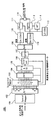
- FIG. 4 shows a configuration of a transmission apparatus 400 using a general OFDM modulator.
- the bit time series which is the input transmission data is converted into time series multi-value symbol data such as 16QAM and 64QAM by the symbol mapping circuit 101 and allocated to OFDM subcarriers.
- “converting to multi-level symbol data” means processing for converting an input bit time series into a plurality of complex data and allocating different subcarriers to each of the complex data.
- Complex data is a complex number including bit information constituting a bit time series
- multilevel symbol data is individual complex data and frequency information of subcarriers to be modulated assigned to the complex data and output. This data includes time (timing) information to be processed, and corresponds to the spectrum of the OFDM signal to be output.
- the multi-level symbol data is converted into parallel multi-level symbol data which is parallel data by the serial-parallel (S / P) conversion circuit 102, and further input to the inverse fast Fourier transform (IFFT) 404, where it is inverted. It is converted into parallel time waveform data which is parallel data by fast Fourier calculation.
- This inverse fast Fourier operation is OFDM modulation.
- the inverse fast Fourier transform is an inverse transform of the fast Fourier transform.
- Fast Fourier transform is an algorithm for calculating discrete Fourier transform at high speed on a computer, and is also used for frequency analysis of a digital signal discretized by signal processing or the like. By inverse fast Fourier transform, spectrum information of discrete sample frequency points is converted into discrete time waveform information.
- the IFFT 404 output parallel time waveform data is converted to serial time-series data by adding a waveform of a guard interval period in a parallel-serial (P / S) conversion and guard interval (GI) addition circuit 405.
- P / S parallel-serial
- GI guard interval
- the processing so far is executed as a complex number operation, but the output of the P / S conversion and GI addition circuit 405 is input to the dividing circuit (splitter) 108, and real component coefficient data and imaginary number component coefficient data are extracted.
- the real component coefficient data is called an in-phase digital baseband signal (I-DBB signal)
- the imaginary component coefficient data is called a quadrature digital baseband signal (Q-DBB signal).
- the I-DBB signal and the Q-DBB signal are respectively converted into in-phase analog baseband signals (I-ABB signals) and quadrature analog baseband signals as analog waveform signals by digital-analog (D / A) converters 109 and 110. After being converted into (Q-ABB signal), they are mixed with carrier LO signals in frequency converters (Mixers) 111 and 112, respectively, and in-phase carrier band signals (I-RF signals) and quadrature carrier band signals (Q -RF signal).
- the output of the local oscillator (LO OSC) 113 is input to the frequency converters 111 and 112 as an LO signal.
- the LO signal to the frequency converter 112 is sent to the frequency converter 111 by the 90 ° phase shifter 114. It is input with a 90 ° phase delay from the LO signal.
- the I-RF signal and the Q-RF signal are combined by the synthesizer 115 and output as a carrier band signal (RF signal).
- An OFDMA (Orthogonal Frequency Division Multiple Access) scheme is a multiple access scheme in which different information transmission destinations are allocated for each subcarrier in the OFDM scheme to simultaneously transmit information to a plurality of partners.
- the number of subcarriers to be allocated, the subcarrier radio modulation scheme, transmission power, and the like can be set in accordance with individual information transmission destinations.
- FIG. 4 schematically shows the case where there are no subcarriers with subcarrier frequencies f 0 to f 4 and f n ⁇ 3 to f n ⁇ 1 , that is, the spectrum is zero.
- f 0 ⁇ f 1 ⁇ f 2 ⁇ f 3 ⁇ f 4 ⁇ f 5 ⁇ ... ⁇ F n-4 ⁇ f n-3 ⁇ f n-2 ⁇ f n-1 .
- a symbol mapping circuit 101 obtains a bit time series that is transmission data, and outputs multi-value symbol data that is a complex number of time series.
- the serial-parallel (S / P) conversion circuit 102 acquires multi-level symbol data and outputs parallel multi-level symbol data which is complex parallel data.
- the subcarrier mapping circuit 103 acquires parallel multi-level symbol data and outputs it to an inverse fast Fourier transform (IFFT) 104, and outputs a frequency and phase control signal, an interpolation control signal, and a frequency point change signal.
- IFFT inverse fast Fourier transform
- the inverse fast Fourier transformer (IFFT) 104 acquires the parallel multilevel symbol data and the frequency point change signal from the subcarrier mapping circuit 103, and among the multilevel symbol data included in the parallel multilevel symbol data, The inverse fast Fourier transform is performed on the complex data of the multilevel symbol data designated by the frequency point change signal, and parallel time waveform data which is a complex number is output.
- IFFT inverse fast Fourier transformer
- a parallel-serial (P / S) conversion and guard interval (GI) addition circuit 105 acquires parallel time waveform data and a frequency point change signal, and complex time series time waveform data to which a waveform of a guard interval period is added. Is output.
- the interpolation circuit 106 obtains complex time series time waveform data and an interpolation control signal, and outputs interpolated time waveform data which is a complex time series.
- the digital frequency converter (DFC) 107 acquires the interpolated time waveform data and the frequency and phase control signal from the subcarrier mapping circuit 103, and outputs a complex digital baseband signal (complex DBB signal) that is a complex number. .
- the guard interval (GI) addition circuit 105, the interpolation circuit 106, and the digital frequency converter (DFC) 107 are assumed to be OFDM modulators. That is, a series of processing from when time-series transmission data is input to when a complex DBB signal is generated is regarded as processing related to OFDM modulation.
- the dividing circuit 108 acquires a complex DBB signal and outputs an in-phase digital baseband signal (I-DBB signal) and a quadrature digital baseband signal (Q-DBB signal).
- I-DBB signal in-phase digital baseband signal
- Q-DBB signal quadrature digital baseband signal
- a digital-analog converter (D / A) 109 and a digital-analog converter (D / A) 110 obtain an I-DBB signal and a Q-DBB signal, respectively, and each an in-phase analog baseband signal (I-ABB signal). ), And outputs an orthogonal analog baseband signal (Q-ABB signal).
- the local oscillator (LO OSC) 113 generates and outputs a local oscillation signal (LO signal).
- the 90 ° phase shifter 114 acquires the LO signal and outputs a quadrature LO signal.
- the frequency converter (Mixer) 111 acquires the I-ABB signal and the LO signal, and outputs an in-phase carrier band signal (I-RF signal).
- the frequency converter (Mixer) 112 acquires the Q-ABB signal and the orthogonal LO signal, and outputs an orthogonal carrier band signal (Q-RF signal).
- the synthesizer 115 acquires the I-RF signal and the Q-RF signal and outputs a carrier band signal (RF signal).
- DFC digital frequency converter
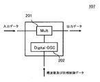
- the interpolated time waveform data input to the DFC 107 is input to the complex multiplier (Mult) 201.
- a digital frequency synthesizer (Digital OSC) 202 acquires a frequency and phase control signal, and outputs a digital LO signal that is a digital sine wave waveform value having a frequency and a phase.
- the complex multiplier (Mult) 201 acquires the interpolated time waveform data and the digital LO signal, and outputs a complex DBB signal.
- the bit time series as transmission data is input to the symbol mapping circuit 101 and converted into multi-value symbol data which is a time series complex number.
- the multi-level symbol data is, for example, a symbol such as 16QAM or 64QAM, and is a complex number including a plurality of bit information.
- the frequency information of the subcarrier to be modulated by the symbol and the time (timing) information to be output are also linked in a time-series order format, for example.
- the multi-level symbol data that is time series is input to the serial-parallel (S / P) conversion circuit 102, converted in parallel, and output as parallel multi-level symbol data.
- the parallel multilevel symbol data is input to the subcarrier mapping circuit 103, and the sublevel mapping is performed based on the multilevel symbol data included in the parallel multilevel symbol data and the frequency information of the subcarrier to be modulated linked to each of the multilevel symbol data.
- the carrier frequency assignment is changed and output to IFFT 104.
- the subcarrier mapping circuit 103 generates a frequency point change signal, generates an interpolation control signal to the IFFT 104 and the P / S conversion and GI addition circuit 105, and outputs the interpolation control signal to the interpolation circuit 106, and outputs the frequency and phase control signal. It is generated and output to the digital frequency converter 107.
- subcarriers are arranged symmetrically with respect to positive and negative frequencies with the frequency 0 as the center.
- the inverse fast Fourier transform calculation amount is proportional to N ⁇ logN.
- N 2048
- N ⁇ log N 15615.219
- N 1024
- N ⁇ log N 7097.827...
- the time for waiting for data input in serial-parallel conversion has been reduced from 2048 to 1024, so that the subsequent computation can be started earlier, and as a result, latency can be reduced.
- the reduction in latency further leads to a reduction in the time zone in which the computing unit is occupied, and as a result, the computing resources required can be reduced.
- the calculation amount can be reduced by generating a sine waveform of the subcarrier by numerical calculation other than the inverse fast Fourier transform or reading the waveform table to substitute for the inverse fast Fourier transform.
- the value is 0 means that both the real part and the imaginary part of the complex data included in the multi-value symbol data are 0, and “the value is not 0” means the multi-value. This means that at least one of the real part and the imaginary part of the complex data included in the symbol data is not zero.
- the subcarrier mapping circuit 103 determines the location of the subcarrier and, based on the result, issues an instruction to change the frequency of the subcarrier and the inverse fast Fourier transform frequency score to the IFFT 104 using the frequency score change signal. .
- the subcarrier mapping circuit 103 determines a range of specific frequency points (a specific frequency band) adjacent to the subcarrier mapping circuit 103 based on the value of the complex data included in the multilevel symbol data.
- the number of frequency points included is output to IFFT 104 as a frequency point number change signal.
- the subcarrier mapping circuit 103 selectively performs frequency shift on complex data to which subcarriers included in a predetermined frequency band are allocated among complex data included in the multilevel symbol data, and IFFT 104 performs inverse fast Fourier transform on each complex data that has been selectively frequency-shifted.
- the subcarrier (non-zero multilevel symbol data) that is actually required to be generated is within 1024 frequency points adjacent to each other.
- a digital frequency converter 107 is provided for frequency and phase shift, and the frequency and phase are compensated based on the frequency and phase control signal from the subcarrier mapping circuit 103.
- the frequency and phase control signal includes information on the frequency shifted by the subcarrier mapping circuit 103 or the phase changed by the shift.
- the interpolation circuit 106 supplements the waveform sampling point data based on the interpolation control signal from the subcarrier mapping circuit 103.
- the interpolation control signal includes information on the number of sampling points of the output waveform to be thinned out because the subcarrier mapping circuit 103 performs frequency shift and frequency point reduction of the subcarrier.
- “information regarding the number of sampling points of the output waveform to be thinned” is, for example, the number of frequency points (number of subcarriers) of parallel multilevel symbol data output from the subcarrier mapping circuit 103.
- the frequency-shifted parallel multilevel symbol data is input to the IFFT 104, subjected to inverse fast Fourier transform based on the frequency point change signal, and converted to complex parallel time waveform data.
- the IFFT 104 can operate or stop the arithmetic circuit in accordance with the frequency point by the frequency point change signal.
- an arithmetic circuit suitable for the number of frequency points can be selected and switched.
- the parameter for setting the operation of the program for performing the arithmetic processing is changed, and the operation suitable for the frequency point is performed.
- the parallel time waveform data is added with a guard interval by the P / S conversion and GI addition circuit 105, and converted to complex time series pre-interpolation time waveform data as serial data.
- the number of parallel time waveform data varies depending on the number of input data of IFFT 104, that is, the number of subcarriers.
- the P / S conversion and GI addition circuit 105 needs to grasp the number of pieces of parallel time waveform data input in advance and operate based on the information. Therefore, the P / S conversion and GI addition circuit 105 executes the above processing based on the frequency point number change signal from the subcarrier mapping circuit 103.
- the pre-interpolation time waveform data is input to the interpolation circuit 106, the waveform data is interpolated based on the interpolation control signal from the subcarrier mapping circuit 103, and is output as time waveform data.
- the time waveform data is input to the digital frequency converter 107, subjected to a frequency shift in the reverse direction by the frequency shifted by the subcarrier mapping circuit 103, and output as a complex DBB signal.
- the phase is also compensated.
- Information on the shift frequency and phase to be compensated is sent from the subcarrier mapping circuit 103 in advance as a frequency and phase control signal.
- the complex DBB signal is input to the dividing circuit 108. Subsequent operations are the same as those of the general OFDM transmitter shown in FIG.
- the time waveform data input to the digital frequency converter 107 is input to a complex multiplier (Mult) 201.
- the frequency and phase control signal input to the digital frequency converter 107 are input to a digital frequency synthesizer (Digital OSC) 202, and the digital frequency synthesizer (Digital OSC) 202 is a complex digital waveform.
- Digital OSC digital frequency synthesizer
- Digital OSC digital frequency synthesizer
- Digital OSC digital frequency synthesizer
- DDS digital synthesizer
- Each unit of the transmission device 100 may be logically realized by a computer program, may be formed as unique hardware, or may be realized as a combination of software and hardware.
- the computer 100 stores the computer program in a readable storage medium.
- the computer reads the computer program from the storage medium and mainly executes the following processing.
- A The input bit string is converted into a plurality of complex data, and different subcarriers are assigned to each of the complex data.
- B A frequency band is determined based on the value of complex data, and complex data to which subcarriers included in the determined frequency band are assigned is selected.
- C An inverse fast Fourier transform (inverse discrete Fourier transform) is performed on the complex data selected in the processing of (b) to generate waveform data.
- D Interpolation of waveform data and frequency shift are performed based on the frequency band determined in the processing of (b).
- this embodiment reduces the number of complex data (number of frequency points) input to the inverse fast Fourier transformer 104, the amount of computation of the inverse fast Fourier transform can be reduced. Therefore, the power consumption of the inverse fast Fourier transformer 104 can be reduced. In addition, it is possible to reduce the latency related to the inverse fast Fourier transform operation.
- the subcarrier mapping circuit 103 and the inverse fast Fourier transformer 104 are set.
- the circuit scale can be reduced. Therefore, the circuit scale of the entire transmission apparatus 100 can be reduced. Furthermore, the manufacturing cost of the transmission device 100 can be reduced.
- the waiting time for data input in the serial-parallel conversion circuit 102 is shortened, and the overall latency can be reduced.
- the latency reduction also leads to a reduction in the time that the computing unit is occupied. As a result, it is possible to reduce computation resources required and divert to other computations. Become.
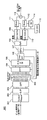
- FIG. 5 shows a configuration of transmitting apparatus 500 using the SC-FDMA scheme based on DFT-Spread OFDM used in the LTE system.
- the SC-FDMA system based on DFT-Spread OFDM (hereinafter referred to as the SC-FDMA system) is an OFDM system input after performing a discrete Fourier transform (DFT) on a symbol sequence to be transmitted.
- DFT discrete Fourier transform
- the bit time series that is input transmission data is converted into time series multi-value symbol data such as 16QAM and 64QAM by the symbol mapping circuit 301, and parallel multi-value by the serial-parallel (S / P) conversion circuit 302. It is converted into symbol data and input to a discrete Fourier transformer (DFT) 303, where it is converted into a plurality of discrete frequency spectrum data by fast Fourier transform.
- DFT discrete Fourier transformer
- the number of sampling points of the discrete Fourier transform is determined according to the symbol rate, which is the number of input multi-level symbol data per unit time. The higher the symbol rate of the multi-level symbol data, the lower the lower.
- the number of frequency spectrum data to be output also corresponds to the symbol rate of the input multilevel symbol data, and the number of frequency spectrum data is large when the symbol rate of multilevel symbol data is high, and the number is low.
- Individual frequency spectrum data corresponds to complex data in the OFDM modulator.
- multilevel symbol data, complex data, and subcarriers correspond one-to-one.
- frequency spectrum data, which is complex data is extracted from a plurality of multilevel symbol data by fast Fourier transform (discrete Fourier transform) of DFT 303.
- the frequency spectrum data has a one-to-one correspondence with subcarriers, but the multi-level symbol data does not have a one-to-one correspondence with them, which is different from the OFDM modulator.
- the symbol mapping circuit 101 of the first embodiment assigns a single subcarrier to a single multi-value symbol data
- the symbol mapping circuit 301 of the present embodiment results in a plurality of multi-values.
- the difference is that a plurality of subcarriers are assigned to the symbol data, and the multilevel symbol data and the subcarriers are associated with each other in an M-to-N manner.
- the frequency spectrum data is assigned to a predetermined subcarrier by the subcarrier mapping circuit 503 and output as a subcarrier spectrum.
- the subcarrier allocation information is given from the upper layer of the system. As described above, in the SC-FDMA system, the multi-value symbol data and the frequency spectrum data derived therefrom are associated with the number of corresponding subcarriers (frequency bandwidth), but the subcarrier frequency is It is not directly associated. Note that the upper hierarchy of the system is a portion not shown in FIG. 5 of the communication system including the transmission device 500. The upper layer of the system may exist inside the transmission apparatus 500 or may exist outside.
- the number of subcarriers used varies according to the symbol rate of multilevel symbol data. Therefore, one transmission apparatus can occupy all subcarriers set in the frequency band assigned as a transmission band, but does not always use all subcarriers at the same time.
- the subcarriers that are not used are used by other transmission apparatuses, so that a plurality of transmission apparatuses can share the same transmission band at the same time, and frequency resources can be used effectively. That is the first feature of the SC-FDMA system.
- a multicarrier system such as the OFDM system has a larger PAPR (Peak to Average Power Ratio) in a radio signal than a single carrier system, and a wireless circuit with lower distortion is required.
- PAPR Peak to Average Power Ratio
- SC-FDMA subcarrier modulation information
- subcarrier modulation information frequency spectrum information
- the time waveform of the radio signal is brought close to the waveform of the single carrier method, and the PAPR is suppressed to a level close to that of the single carrier method, thereby reducing the low distortion characteristics required of the radio circuit. It is relaxed.
- SC-FDMA Single Carrier-Frequency Division Multiple Access
- the frequency of the subcarrier to be used can be easily changed by switching the subcarrier mapping.
- the LTE system realizes a frequency hopping function.
- the subcarrier mapping circuit 503 assigns the output of the DFT 303 to the subcarriers (frequency f 5 to f n-4 ) while maintaining the relative frequency arrangement, and unused subcarriers (from the frequency f 0).
- “0” is output, that is, a case where there is no subcarrier is schematically shown.
- f 0 ⁇ f 1 ⁇ f 2 ⁇ f 3 ⁇ f 4 ⁇ f 5 ⁇ ... ⁇ F n-4 ⁇ f n-3 ⁇ f n-2 ⁇ f n-1 .
- the output of the subcarrier mapping circuit 503 is input to an inverse fast Fourier transformer (IFFT) 404, where it is converted into a time waveform by inverse fast Fourier calculation.
- IFFT inverse fast Fourier transformer
- Formula (1) is one of the definition formulas related to the SC-FDMA scheme shown in the 3GPP TS 36.211 specification.
- generated based on the frequency spectrum data of a subcarrier is shown.
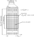
- FIG. 6 shows Resource grid representing the arrangement of frequency spectrum data on the subcarrier frequency-time plane.
- S l (t) on the left side is a complex display of the I-ABB signal output from the D / A converter 109 and the Q-ABB signal output from the D / A converter 110 together.
- Ak ( ⁇ ), l on the right side corresponds to the frequency spectrum data that is the output of the subcarrier mapping circuit 503.
- N 2048
- N ⁇ log N 15615.219.
- the transmitter 300 uses the modulator of the present invention.
- a serial-parallel (S / P) conversion circuit 302 acquires multi-level symbol data which is a time-series complex number output from the symbol mapping circuit 301 and outputs parallel multi-level symbol data.
- a discrete Fourier transformer (DFT) 303 acquires parallel multilevel symbol data and outputs discrete frequency spectrum data.
- the subcarrier mapping circuit 304 acquires frequency spectrum data, outputs it to the IFFT 104, and outputs a frequency point change signal, frequency and phase control data, and interpolation control data.
- the time-series multi-value symbol data generated by the symbol mapping circuit 301 is input to the S / P conversion circuit 302, subjected to parallel conversion, and output as parallel multi-value symbol data.
- the parallel multilevel symbol data is input to the DFT 303, subjected to discrete Fourier transform, and output as discrete frequency spectrum data that is a complex number.
- subcarriers corresponding to each are generated by inverse fast Fourier transform using amplitude information and phase information included in individual frequency spectrum data.
- Individual frequency spectrum data is linked with frequency information of subcarriers in a subcarrier mapping circuit 304.
- the frequency spectrum data is input to the subcarrier mapping circuit 304, and the allocation of the subcarrier frequency is changed based on the value of the frequency spectrum data and the frequency information of the subcarrier designated from the system upper layer to be allocated to each. , Output to IFFT 104.
- the system upper layer is a portion not shown in FIG. 3 of the communication system including the transmission device 300.
- the upper hierarchy of the system may exist inside the transmission apparatus 300 or may exist outside.
- the subcarrier mapping circuit 304 generates a frequency point number change signal and outputs it to the IFFT 104 and the P / S conversion and GI addition circuit 105, generates an interpolation control signal and outputs it to the interpolation circuit 106, and further, the frequency and phase.
- a control signal is generated and output to the digital frequency converter 107.
- the SC-FDMA system is characterized in that subcarriers are locally arranged on the frequency axis, among many systems using OFDM modulation.
- subcarrier frequency allocation information including subcarrier localization information is given from the upper layer of the system. Based on this information, the subcarrier mapping circuit 304 generates a frequency point change signal, an interpolation control signal, a frequency and a phase control signal in addition to subcarrier frequency assignment.
- Expression (2) indicates the number of subcarriers that can exist in the Uplink band.
- Equation (3) k ( ⁇ ) in equation (1) is defined by equation (3).
- l is a serial number assigned to identify the SC-FDMA symbol in the time axis direction.
- k is a serial number assigned to identify the frequency of subcarriers that can exist in the Uplink band. It should be noted that subcarriers that are not allocated to the OFDM modulator in this SC-FDMA scheme (for example, subcarriers used by other transmission apparatuses in the same Uplink band) are also included.
- a k, l is the content (namely, frequency spectrum data) of the resource element (k, l).
- Resource elements relating to subcarriers not assigned to this SC-FDMA OFDM modulator are also included, but they have a value of zero.
- ⁇ f is a subcarrier frequency interval and is fixed at 15 kHz.
- N CP, l is the length of the cyclic prefix expressed in units of basic time units.
- T s is the time length of the basic time unit and is 1 / (30.72 MHz).
- N CP, l T s is the cyclic prefix time length associated with the first SC-FDMA symbol.
- FIG. 6 shows a resource grid that represents the arrangement of frequency spectrum data on the subcarrier frequency-time plane.
- the number of subcarriers allocated to the SC-FDMA OFDM modulation is N. Since these are continuously assigned to adjacent subcarriers, it is assumed that they are assigned to the (k s ,..., K s + N ⁇ 1) -th subcarrier in the analog baseband signal of the SC-FDMA system, and a k ( ⁇ ) And l are defined as in equation (4) using z (k ⁇ k s ).
- the expression (1) can be expressed as the expression (5) by substituting the expression (4).
- m k ⁇ k s .
- Equation (5) represents an analog baseband signal for an SC-FDMA symbol, but replacing the inverse Fourier transform with a discrete inverse Fourier transform corresponds to replacing it with a display as a digital baseband signal.
- Equation (7) is obtained when N subcarriers arranged at the (k s ,..., K s + N ⁇ 1) th are used in SC-FDMA digital baseband signal generation. It is shown that the same result can be obtained even if the inverse Fourier transform is performed on the subcarriers to generate a waveform signal and the digital LO signal, which is a complex digital waveform, is multiplied there. That is, the waveform signal generated by the inverse Fourier transform is represented by the following equation (8), and the digital LO signal is represented by the following equation (9).
- the digital frequency synthesizer (Digital OSC) 202 generates a digital LO signal based on the above, and the complex multiplier (Mult) 201 performs multiplication.
- the OFDM modulator of the present invention is applied to an SC-FDMA transmission apparatus, but may be used for transmission apparatuses of other systems.
Abstract
Description
図4に、一般的なOFDM変調器を用いた送信装置400の構成を示す。
次に図1の送信装置100の動作について説明する。
(a)入力されたビット列を、複数の複素データに変換し、複素データの夫々に異なるサブキャリアを割り当てる。
(b)複素データの値に基づいて周波数帯域を定め、定められた周波数帯域に含まれるサブキャリアが割り当てられた複素データを選択する。
(c)(b)の処理で選択された複素データに対して逆高速フーリエ変換(逆離散フーリエ変換)を行い、波形データを生成する。
(d)(b)の処理で定められた周波数帯域に基づいて、波形データの補間と周波数シフトを行う。
図5に、LTEシステムで使用されるDFT-Spread OFDMに基づくSC-FDMA方式を用いた送信装置500の構成を示す。


lは、SC-FDMAシンボルを時間軸方向で識別するために付与された連番である。
kは、Uplink帯域内に存在できるサブキャリアの周波数を識別するために付与された連番である。なお、このSC-FDMA方式におけるOFDM変調器に割り当てられていないサブキャリア(例えば、同じUplink帯域内で他の送信装置が使用するサブキャリア)も含んでいることに注意する必要がある。
ak,lは、Resource element(k,l)の内容(つまり周波数スペクトルデータ)である。このSC-FDMA方式のOFDM変調器に割り当てられていないサブキャリアに関するResource elementも含まれるが、それらは値が0となる。
Δfは、サブキャリアの周波数間隔で、15kHzに固定されている。
(k+1/2)Δfは、k番目のサブキャリアに関する帯域中央からのオフセット周波数である。
NCP,lは、Basic time unit単位で表したCyclic prefixの長さである。
Tsは、Basic time unitの時間長で、1/(30.72MHz)である。
NCP,lTsは、l番目のSC-FDMAシンボルに関し、先頭に付くCyclic prefixの時間長である。


Claims (10)
- 夫々に異なるサブキャリアが割り当てられた複数の複素データを取得し、当該取得された複数の前記複素データから波形データを生成する第1回路と、
前記第1回路によって生成された前記波形データを取得し、当該波形データを周波数シフトする第2回路と、
を備えることを特徴とするOFDM変調器。 - 請求項1に記載のOFDM変調器であって、
前記第1回路は、各々の前記複素データに対して逆離散フーリエ変換を行うことによって前記波形データを生成することを特徴とするOFDM変調器。 - 請求項1または2に記載のOFDM変調器であって、
前記第2回路は、シフトされる周波数に相当するデジタル信号を生成し、前記波形データに対して前記デジタル信号を乗算することによって、当該波形データを周波数シフトすることを特徴とするOFDM変調器。 - 請求項1乃至3いずれか一項に記載のOFDM変調器であって、
取得したビット列を、複数の多値シンボルデータに変換し、前記多値シンボルデータの夫々に異なる前記サブキャリアを割り当てる第3回路と、
前記第3回路から取得した複数の前記多値シンボルデータの一部を選択し、選択された前記多値シンボルデータに割り当てられた前記サブキャリアを周波数シフトして出力する第4回路を備え、
前記第1回路は、前記第4回路から出力された前記多値シンボルデータの夫々を前記複素データとして取得し、当該多値シンボルデータから前記波形データを生成し、
前記第2回路は、前記第4回路によってシフトされた周波数分、当該波形データを逆方向に周波数シフトすることを特徴とするOFDM変調器。 - 請求項4に記載のOFDM変調器であって、
前記第4回路は、取得した複数の前記多値シンボルデータのうち、実部または虚部の少なくとも一方が0ではない前記多値シンボルデータに割り当てられた前記サブキャリアが局在する周波数帯域を定め、当該周波数帯域に含まれる前記サブキャリアの中央値を0に周波数シフトすることを特徴とするOFDM変調器。 - 請求項1乃至3いずれか一項に記載のOFDM変調器であって、
取得したビット列を、複数の多値シンボルデータに変換する第5回路と、
前記第5回路によって変換された複数の前記多値シンボルデータから、離散フーリエ変換によって複数の周波数スペクトルデータを抽出する第6回路と、
前記第6回路から取得した前記周波数スペクトルデータに対して予め定められた前記サブキャリアを割り当てて出力する第7回路を備え、
前記第1回路は、前記第7回路から出力された前記周波数スペクトルデータの夫々を前記複素データとして取得し、取得された前記周波数スペクトルデータから前記波形データを生成することを特徴とするOFDM変調器。 - 請求項4乃至6いずれか一項に記載のOFDM変調器であって、
間引かれた出力波形のサンプリング点数に関する情報に基づいて、前記波形データを補間する第8回路を備えることを特徴とするOFDM変調器。 - 夫々に異なるサブキャリアが割り当てられた複数の複素データを取得し、当該取得された複数の前記複素データから波形データを生成する第1回路と、
前記第1回路によって生成された前記波形データを取得し、当該波形データを周波数シフトする第2回路と、
を備える変調器を有することを特徴とするOFDM送信装置。 - 夫々に異なるサブキャリアが割り当てられた複数の複素データを取得し、
前記取得された複数の前記複素データから波形データを生成し、
前記生成された前記波形データを取得し、
前記波形データを周波数シフトする、
ことを含むOFDM変調方法。 - コンピュータが読み出し可能な記憶媒体であって、
夫々に異なるサブキャリアが割り当てられた複数の複素データを取得し、取得された複数の前記複素データから波形データを生成する第1処理と、
前記第1処理で生成された前記波形データを取得し、当該波形データを周波数シフトする第2処理と、
を前記コンピュータに実行させるプログラムを格納する記憶媒体。
Priority Applications (5)
| Application Number | Priority Date | Filing Date | Title |
|---|---|---|---|
| JP2012510547A JP5734960B2 (ja) | 2010-04-13 | 2011-03-30 | Ofdm変調器、ofdm送信装置、及びofdm変調方法並びにプログラム |
| US13/640,148 US9031154B2 (en) | 2010-04-13 | 2011-03-30 | OFDM modulator, OFDM transmission device, and OFDM modulation method |
| CN201180018215.0A CN102835048B (zh) | 2010-04-13 | 2011-03-30 | Ofdm调制器、ofdm发送设备和ofdm调制方法 |
| EP11768590.9A EP2560305A4 (en) | 2010-04-13 | 2011-03-30 | Ofdm modulator, ofdm transmission apparatus, and ofdm modulation method |
| US14/529,408 US9596117B2 (en) | 2010-04-13 | 2014-10-31 | OFDM modulator, OFDM transmission device, and OFDM modulation method |
Applications Claiming Priority (2)
| Application Number | Priority Date | Filing Date | Title |
|---|---|---|---|
| JP2010-092318 | 2010-04-13 | ||
| JP2010092318 | 2010-04-13 |
Related Child Applications (2)
| Application Number | Title | Priority Date | Filing Date |
|---|---|---|---|
| US13/640,148 A-371-Of-International US9031154B2 (en) | 2010-04-13 | 2011-03-30 | OFDM modulator, OFDM transmission device, and OFDM modulation method |
| US14/529,408 Continuation US9596117B2 (en) | 2010-04-13 | 2014-10-31 | OFDM modulator, OFDM transmission device, and OFDM modulation method |
Publications (1)
| Publication Number | Publication Date |
|---|---|
| WO2011129064A1 true WO2011129064A1 (ja) | 2011-10-20 |
Family
ID=44798452
Family Applications (1)
| Application Number | Title | Priority Date | Filing Date |
|---|---|---|---|
| PCT/JP2011/001927 WO2011129064A1 (ja) | 2010-04-13 | 2011-03-30 | Ofdm変調器、ofdm送信装置、及びofdm変調方法 |
Country Status (5)
| Country | Link |
|---|---|
| US (2) | US9031154B2 (ja) |
| EP (1) | EP2560305A4 (ja) |
| JP (2) | JP5734960B2 (ja) |
| CN (1) | CN102835048B (ja) |
| WO (1) | WO2011129064A1 (ja) |
Families Citing this family (8)
| Publication number | Priority date | Publication date | Assignee | Title |
|---|---|---|---|---|
| US9031154B2 (en) * | 2010-04-13 | 2015-05-12 | Lenovo Innovations Limited (Hong Kong) | OFDM modulator, OFDM transmission device, and OFDM modulation method |
| CN106034265B (zh) * | 2015-03-13 | 2020-01-10 | 上海诺基亚贝尔股份有限公司 | 用于无源光网络中的混合复用/解复用的方法及装置 |
| WO2017041273A1 (en) * | 2015-09-10 | 2017-03-16 | Huawei Technologies Co., Ltd. | A data transmission method and apparatus |
| WO2017081980A1 (ja) * | 2015-11-10 | 2017-05-18 | 三菱電機株式会社 | 送信装置、通信装置、送信信号生成方法、受信装置および復調方法 |
| DE102016102005B4 (de) * | 2016-02-04 | 2018-08-02 | Rheinisch-Westfälische Technische Hochschule Aachen (RWTH) | Schaltungsanordnung und Verfahren zur Erzeugung eines hochfrequenten, analogen Sendesignals |
| KR102409785B1 (ko) * | 2017-03-23 | 2022-06-16 | 삼성전자주식회사 | 무선 통신 시스템에서 초기 접속을 수행하기 위한 장치 및 방법 |
| WO2020125966A1 (en) * | 2018-12-19 | 2020-06-25 | Huawei Technologies Co., Ltd. | Transmitter device and receiver device and methods thereof |
| CN116438766A (zh) * | 2020-10-15 | 2023-07-14 | 华为技术有限公司 | 一种传输信号的方法及装置 |
Citations (7)
| Publication number | Priority date | Publication date | Assignee | Title |
|---|---|---|---|---|
| JPH11346203A (ja) * | 1998-06-02 | 1999-12-14 | Matsushita Electric Ind Co Ltd | Ofdma信号伝送装置及び方法 |
| JP2000307543A (ja) * | 1999-04-19 | 2000-11-02 | Victor Co Of Japan Ltd | マルチキャリア送信、受信及び伝送システム |
| JP2008078790A (ja) * | 2006-09-19 | 2008-04-03 | Toshiba Corp | Ofdm送信機 |
| JP2009194732A (ja) * | 2008-02-15 | 2009-08-27 | Ntt Docomo Inc | 無線通信装置及び無線通信方法 |
| JP2009239539A (ja) | 2008-03-26 | 2009-10-15 | Panasonic Corp | Sc−fdma送信装置及びsc−fdma送信信号形成方法 |
| JP2010092318A (ja) | 2008-10-09 | 2010-04-22 | Nec Corp | ディスクアレイサブシステム、ディスクアレイサブシステムのキャッシュ制御方法、及びプログラム |
| JP2011029720A (ja) * | 2009-07-21 | 2011-02-10 | Mitsubishi Electric Corp | 衛星通信装置および衛星通信システム |
Family Cites Families (6)
| Publication number | Priority date | Publication date | Assignee | Title |
|---|---|---|---|---|
| US6441683B1 (en) * | 2000-08-16 | 2002-08-27 | Advanced Micro Devices, Inc | Device and method for recovering frequency redundant data in a network communications receiver |
| JP2003224538A (ja) * | 2002-01-28 | 2003-08-08 | Matsushita Electric Ind Co Ltd | 送信装置及び送信信号生成方法並びに受信装置及び受信信号処理方法 |
| US7822007B2 (en) * | 2005-08-23 | 2010-10-26 | Electronics And Telecommunications Research Institute | Transmitter in FDMA communication system and method for configuring pilot channel |
| JP4952088B2 (ja) | 2006-06-23 | 2012-06-13 | ソニー株式会社 | 送信装置、送信方法、受信装置、受信方法及び伝送システム |
| EP2169890B1 (en) * | 2008-09-25 | 2011-03-09 | Telefonaktiebolaget L M Ericsson (publ) | OFDM signal processing |
| US9031154B2 (en) * | 2010-04-13 | 2015-05-12 | Lenovo Innovations Limited (Hong Kong) | OFDM modulator, OFDM transmission device, and OFDM modulation method |
-
2011
- 2011-03-30 US US13/640,148 patent/US9031154B2/en not_active Expired - Fee Related
- 2011-03-30 WO PCT/JP2011/001927 patent/WO2011129064A1/ja active Application Filing
- 2011-03-30 EP EP11768590.9A patent/EP2560305A4/en not_active Withdrawn
- 2011-03-30 JP JP2012510547A patent/JP5734960B2/ja not_active Expired - Fee Related
- 2011-03-30 CN CN201180018215.0A patent/CN102835048B/zh not_active Expired - Fee Related
-
2014
- 2014-10-31 US US14/529,408 patent/US9596117B2/en not_active Expired - Fee Related
-
2015
- 2015-03-13 JP JP2015050223A patent/JP5924847B2/ja not_active Expired - Fee Related
Patent Citations (7)
| Publication number | Priority date | Publication date | Assignee | Title |
|---|---|---|---|---|
| JPH11346203A (ja) * | 1998-06-02 | 1999-12-14 | Matsushita Electric Ind Co Ltd | Ofdma信号伝送装置及び方法 |
| JP2000307543A (ja) * | 1999-04-19 | 2000-11-02 | Victor Co Of Japan Ltd | マルチキャリア送信、受信及び伝送システム |
| JP2008078790A (ja) * | 2006-09-19 | 2008-04-03 | Toshiba Corp | Ofdm送信機 |
| JP2009194732A (ja) * | 2008-02-15 | 2009-08-27 | Ntt Docomo Inc | 無線通信装置及び無線通信方法 |
| JP2009239539A (ja) | 2008-03-26 | 2009-10-15 | Panasonic Corp | Sc−fdma送信装置及びsc−fdma送信信号形成方法 |
| JP2010092318A (ja) | 2008-10-09 | 2010-04-22 | Nec Corp | ディスクアレイサブシステム、ディスクアレイサブシステムのキャッシュ制御方法、及びプログラム |
| JP2011029720A (ja) * | 2009-07-21 | 2011-02-10 | Mitsubishi Electric Corp | 衛星通信装置および衛星通信システム |
Non-Patent Citations (1)
| Title |
|---|
| See also references of EP2560305A4 |
Also Published As
| Publication number | Publication date |
|---|---|
| US20130028347A1 (en) | 2013-01-31 |
| EP2560305A1 (en) | 2013-02-20 |
| US20150043324A1 (en) | 2015-02-12 |
| CN102835048A (zh) | 2012-12-19 |
| US9596117B2 (en) | 2017-03-14 |
| JP5924847B2 (ja) | 2016-05-25 |
| US9031154B2 (en) | 2015-05-12 |
| JPWO2011129064A1 (ja) | 2013-07-11 |
| JP2015111950A (ja) | 2015-06-18 |
| CN102835048B (zh) | 2016-08-17 |
| JP5734960B2 (ja) | 2015-06-17 |
| EP2560305A4 (en) | 2017-06-14 |
Similar Documents
| Publication | Publication Date | Title |
|---|---|---|
| JP5924847B2 (ja) | Ofdm変調器、ofdm送信装置、及びofdm変調方法並びにプログラム | |
| JP2008125070A (ja) | Ofdm通信装置及び方法 | |
| WO2007148584A1 (ja) | 可変帯域で通信するための装置及び方法 | |
| KR20160092837A (ko) | 다중 반송파 통신 시스템에서 전력을 제어하는 방법 및 장치 | |
| JP2000261403A (ja) | 送信装置および方法、並びに提供媒体 | |
| US10277448B1 (en) | Method for hierarchical modulation with vector processing | |
| JP2007020072A (ja) | 無線通信システム、無線通信装置及び無線通信方法 | |
| KR20090059315A (ko) | 통신시스템에서 역 고속 퓨리에 변환 방법 및 장치 | |
| JP3541674B2 (ja) | マルチキャリア信号の生成方法及び送信装置 | |
| JP2013093746A (ja) | 通信機および通信方法 | |
| JP5871210B2 (ja) | 無線通信システム、送信機およびマルチキャリア通信方法 | |
| KR100768327B1 (ko) | 다중 반송파 신호를 사용하는 시스템의 cinr 추정장치 및 그 방법 | |
| Kadhum et al. | Digital chunk processing with orthogonal GFDM doubles wireless channel capacity | |
| US7916622B2 (en) | Apparatus and method for allocating resources in mobile communication system | |
| JP5799463B2 (ja) | 無線通信システム、送信機およびマルチキャリア通信方法 | |
| JP5407562B2 (ja) | 送信装置 | |
| JP5151614B2 (ja) | Ofdmaを利用する信号伝送装置 | |
| KR101400926B1 (ko) | 신호 송신 장치 및 방법 | |
| JP6858405B2 (ja) | 通信方法及び通信機 | |
| JP5892599B2 (ja) | Ofdm(直交周波数分割多重)復調器およびofdm伝送システムならびにofdm復調方法 | |
| JP5204256B2 (ja) | 無線通信システム、無線通信装置及び無線通信方法 | |
| TWI469590B (zh) | 副載波不需重排序的ofdm接收器及ofdm信號處理方法 | |
| CN111327555A (zh) | 一种正交频分复用系统及信号输出方法 | |
| JP2009135970A (ja) | 送信装置 | |
| JP2009135971A (ja) | 送信装置 |
Legal Events
| Date | Code | Title | Description |
|---|---|---|---|
| WWE | Wipo information: entry into national phase |
Ref document number: 201180018215.0 Country of ref document: CN |
|
| 121 | Ep: the epo has been informed by wipo that ep was designated in this application |
Ref document number: 11768590 Country of ref document: EP Kind code of ref document: A1 |
|
| WWE | Wipo information: entry into national phase |
Ref document number: 2011768590 Country of ref document: EP |
|
| WWE | Wipo information: entry into national phase |
Ref document number: 2012510547 Country of ref document: JP |
|
| WWE | Wipo information: entry into national phase |
Ref document number: 13640148 Country of ref document: US |
|
| WWE | Wipo information: entry into national phase |
Ref document number: 8773/CHENP/2012 Country of ref document: IN |
|
| NENP | Non-entry into the national phase |
Ref country code: DE |