WO2011125853A1 - 圧電膜型デバイスの製造方法 - Google Patents
圧電膜型デバイスの製造方法 Download PDFInfo
- Publication number
- WO2011125853A1 WO2011125853A1 PCT/JP2011/058251 JP2011058251W WO2011125853A1 WO 2011125853 A1 WO2011125853 A1 WO 2011125853A1 JP 2011058251 W JP2011058251 W JP 2011058251W WO 2011125853 A1 WO2011125853 A1 WO 2011125853A1
- Authority
- WO
- WIPO (PCT)
- Prior art keywords
- mask
- piezoelectric
- cavity
- material layer
- photosensitive film
- Prior art date
- Legal status (The legal status is an assumption and is not a legal conclusion. Google has not performed a legal analysis and makes no representation as to the accuracy of the status listed.)
- Ceased
Links
Images










Classifications
-
- B—PERFORMING OPERATIONS; TRANSPORTING
- B41—PRINTING; LINING MACHINES; TYPEWRITERS; STAMPS
- B41J—TYPEWRITERS; SELECTIVE PRINTING MECHANISMS, i.e. MECHANISMS PRINTING OTHERWISE THAN FROM A FORME; CORRECTION OF TYPOGRAPHICAL ERRORS
- B41J2/00—Typewriters or selective printing mechanisms characterised by the printing or marking process for which they are designed
- B41J2/005—Typewriters or selective printing mechanisms characterised by the printing or marking process for which they are designed characterised by bringing liquid or particles selectively into contact with a printing material
- B41J2/01—Ink jet
- B41J2/135—Nozzles
- B41J2/16—Production of nozzles
- B41J2/1607—Production of print heads with piezoelectric elements
- B41J2/161—Production of print heads with piezoelectric elements of film type, deformed by bending and disposed on a diaphragm
-
- B—PERFORMING OPERATIONS; TRANSPORTING
- B41—PRINTING; LINING MACHINES; TYPEWRITERS; STAMPS
- B41J—TYPEWRITERS; SELECTIVE PRINTING MECHANISMS, i.e. MECHANISMS PRINTING OTHERWISE THAN FROM A FORME; CORRECTION OF TYPOGRAPHICAL ERRORS
- B41J2/00—Typewriters or selective printing mechanisms characterised by the printing or marking process for which they are designed
- B41J2/005—Typewriters or selective printing mechanisms characterised by the printing or marking process for which they are designed characterised by bringing liquid or particles selectively into contact with a printing material
- B41J2/01—Ink jet
- B41J2/135—Nozzles
- B41J2/16—Production of nozzles
- B41J2/1621—Manufacturing processes
- B41J2/1631—Manufacturing processes photolithography
-
- B—PERFORMING OPERATIONS; TRANSPORTING
- B41—PRINTING; LINING MACHINES; TYPEWRITERS; STAMPS
- B41J—TYPEWRITERS; SELECTIVE PRINTING MECHANISMS, i.e. MECHANISMS PRINTING OTHERWISE THAN FROM A FORME; CORRECTION OF TYPOGRAPHICAL ERRORS
- B41J2/00—Typewriters or selective printing mechanisms characterised by the printing or marking process for which they are designed
- B41J2/005—Typewriters or selective printing mechanisms characterised by the printing or marking process for which they are designed characterised by bringing liquid or particles selectively into contact with a printing material
- B41J2/01—Ink jet
- B41J2/135—Nozzles
- B41J2/16—Production of nozzles
- B41J2/1621—Manufacturing processes
- B41J2/164—Manufacturing processes thin film formation
- B41J2/1645—Manufacturing processes thin film formation thin film formation by spincoating
-
- B—PERFORMING OPERATIONS; TRANSPORTING
- B41—PRINTING; LINING MACHINES; TYPEWRITERS; STAMPS
- B41J—TYPEWRITERS; SELECTIVE PRINTING MECHANISMS, i.e. MECHANISMS PRINTING OTHERWISE THAN FROM A FORME; CORRECTION OF TYPOGRAPHICAL ERRORS
- B41J2/00—Typewriters or selective printing mechanisms characterised by the printing or marking process for which they are designed
- B41J2/005—Typewriters or selective printing mechanisms characterised by the printing or marking process for which they are designed characterised by bringing liquid or particles selectively into contact with a printing material
- B41J2/01—Ink jet
- B41J2/135—Nozzles
- B41J2/16—Production of nozzles
- B41J2/1621—Manufacturing processes
- B41J2/164—Manufacturing processes thin film formation
- B41J2/1646—Manufacturing processes thin film formation thin film formation by sputtering
-
- H—ELECTRICITY
- H10—SEMICONDUCTOR DEVICES; ELECTRIC SOLID-STATE DEVICES NOT OTHERWISE PROVIDED FOR
- H10N—ELECTRIC SOLID-STATE DEVICES NOT OTHERWISE PROVIDED FOR
- H10N30/00—Piezoelectric or electrostrictive devices
- H10N30/01—Manufacture or treatment
- H10N30/08—Shaping or machining of piezoelectric or electrostrictive bodies
-
- H—ELECTRICITY
- H10—SEMICONDUCTOR DEVICES; ELECTRIC SOLID-STATE DEVICES NOT OTHERWISE PROVIDED FOR
- H10N—ELECTRIC SOLID-STATE DEVICES NOT OTHERWISE PROVIDED FOR
- H10N30/00—Piezoelectric or electrostrictive devices
- H10N30/20—Piezoelectric or electrostrictive devices with electrical input and mechanical output, e.g. functioning as actuators or vibrators
- H10N30/204—Piezoelectric or electrostrictive devices with electrical input and mechanical output, e.g. functioning as actuators or vibrators using bending displacement, e.g. unimorph, bimorph or multimorph cantilever or membrane benders
- H10N30/2047—Membrane type
Definitions
- the present invention relates to a method for manufacturing a piezoelectric film type device.
- a piezoelectric film type device including a substrate having a hollow portion and a piezoelectric element provided on the substrate is known.
- the piezoelectric element includes a first electrode, a second electrode, and a piezoelectric film sandwiched between the first electrode and the second electrode.
- the piezoelectric film type device the piezoelectric film is expanded and contracted by a voltage applied between the first electrode and the second electrode.
- a part of the substrate for example, a diaphragm
- Such a piezoelectric film type device is used, for example, as an ink jet actuator for a printer.
- piezoelectric and “electrostrictive” are expressed as “piezoelectric” for convenience. Therefore, for example, in this specification and the like, “piezoelectric element” includes both “an element having a piezoelectric effect (piezoelectric element) and an element having an electrostrictive effect (electrostrictive element)”, and “piezoelectric film” is “ Both “piezoelectric film and electrostrictive film” are included.
- the “piezoelectric film type device” in this specification and the like includes “a device including a piezoelectric element and a device including an electrostrictive element”.
- a substrate having a cavity is bonded to a piezoelectric element including a fired piezoelectric film.
- a mask is formed on the piezoelectric element, and fine particles (abrasive grains) are ejected to remove the piezoelectric element in the portion where the mask is not present. That is, the piezoelectric element is processed by so-called “blast processing” (see, for example, Patent Document 1).
- the mask (mask for blasting) is usually formed as follows. (1) A photosensitive resin is applied to the entire surface of the piezoelectric element by a film thickness forming method, thereby forming a photosensitive resin layer. (2) A shield having a predetermined shape is provided on the photosensitive resin layer. (3) The photosensitive resin is exposed by irradiating the piezoelectric element with light from above the shield. (4) One of “exposed photosensitive resin” and “photosensitive resin not exposed due to the presence of the shielding” is removed, thereby forming the mask.
- Patent No. 3340043 paragraphs 0040, 0042, etc.
- the piezoelectric element including the fired piezoelectric film has high hardness. Furthermore, when a fine piezoelectric element is formed by blasting, it is difficult to use abrasive grains having a large diameter or to set the projection pressure to a very high value. As a result, according to the conventional manufacturing method, the time required for blasting is long and the production efficiency is not good. Accordingly, one of the objects of the present invention is to provide a method for manufacturing a piezoelectric film type device capable of efficiently manufacturing a piezoelectric film type device.
- the method for manufacturing a piezoelectric film type device of the present invention includes a substrate, a piezoelectric film, and a piezoelectric element disposed on the first main surface of the substrate.
- a method of manufacturing a piezoelectric film type device comprising: (A) a substrate preparation step of preparing the substrate; (B) a piezoelectric material layer forming step of forming a piezoelectric material layer, which is a layer containing a piezoelectric material before firing that changes into the piezoelectric film by firing, above the first main surface of the substrate; (C) a first mask creating step of forming a first mask above the piezoelectric material layer; (D) A piezoelectric material that removes the piezoelectric material layer present in a portion where the first mask does not exist by projecting a projection material containing at least one of abrasive grains and an organic solvent toward the first main surface of the substrate.
- a material layer processing step ;
- (F) a firing step of firing the piezoelectric material layer including.
- the piezoelectric material layer is formed above the first main surface (upper surface) of the substrate (see the piezoelectric material layer forming step (b)).
- This piezoelectric material layer is a layer that changes into a piezoelectric film upon firing, and includes a piezoelectric material before firing.
- a first mask is formed above the piezoelectric material layer (see the first mask creating step (c)).
- the projection material containing at least one of abrasive grains and an organic solvent is projected toward the first main surface of the substrate, whereby the piezoelectric material layer present in the portion where the first mask does not exist is removed.
- piezoelectric material layer processing step (d). That is, processing corresponding to blast processing is performed on the “piezoelectric material layer before firing”. Since the piezoelectric material layer before firing has a lower hardness than the fired piezoelectric film, it can be easily processed by projecting a projection material. That is, blasting can be performed at a high processing rate. As a result, a piezoelectric film type device can be manufactured efficiently.
- the piezoelectric element is within a range in which the cavity portion of the substrate is projected in the “direction orthogonal to the first main surface (surface on which the diaphragm is present) of the substrate”. It is important that it is provided.
- a direction orthogonal to the first main surface of the substrate is referred to as a “first main surface orthogonal direction”.
- an inkjet actuator or the like a plurality of cavities are provided in a substrate, and a piezoelectric element is provided in a cavity projection region for each of the cavities.
- the positional relationship (relative position) of the actual piezoelectric element with respect to the cavity projection region is different between the plurality of cavities, the ink ejection capabilities between the plurality of cavities are different from each other. Therefore, there is a demand for a manufacturing method capable of accurately forming the piezoelectric element “on the first main surface of the substrate and in the cavity projection region”. Such a manufacturing method is even more important when the piezoelectric film type device is miniaturized.
- the positional accuracy of the piezoelectric element depends on the positional accuracy of the blasting mask. Furthermore, the positional accuracy of the blasting mask depends on the positional accuracy of the shield.
- the shield is formed at a position based on a marking provided on the upper surface of the substrate. Therefore, it is not easy to match the area where the shield is present and the cavity projection area with high accuracy. This is because, for example, the shape of the cavity itself is not constant and / or the relative positional relationship between the cavity and the marking is not necessarily constant. As a result, the piezoelectric element may not be formed in such a way that its existence area accurately matches the cavity projection area.
- another object of the present invention is to efficiently form the piezoelectric element so that the region where the film-type piezoelectric element exists is on the upper surface of the substrate and precisely coincides with the cavity projection region. It is in providing the manufacturing method which can be performed.
- the substrate has a cavity.
- the piezoelectric element includes a first electrode and a second electrode, and a piezoelectric film formed so as to be sandwiched between the first electrode and the second electrode. Further, the piezoelectric element is configured to display an “image obtained by projecting the cavity” in a “direction orthogonal to the first main surface (a direction orthogonal to the first main surface)” with respect to the first main surface of the substrate. It is provided so as to coincide with a spatial region (cavity projection region) formed by extending in the direction orthogonal to one main surface. That is, the piezoelectric element is provided so that the location and outline of the piezoelectric element coincide with the location and outline of the cavity projection region in plan view.
- the piezoelectric film type device changes the volume of the cavity by expansion and contraction of the piezoelectric element based on voltage application between the first electrode and the second electrode.
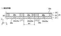
- the substrate preparation step (a) is a step of preparing the substrate having the cavity
- the first mask creating step (c) (C1) a photosensitive film forming step of forming a first photosensitive film above the piezoelectric material layer; (C2) By irradiating the substrate with light parallel to the direction orthogonal to the first main surface from the second main surface side of the substrate facing the first main surface, the inside of the cavity projection region A first exposure step of exposing the first photosensitive film existing outside the cavity projection region without exposing the existing first photosensitive film; and (C3) a post-exposure first photosensitive film removing step of forming a first mask on the upper surface of the piezoelectric material layer by removing the exposed first photosensitive film; including.
- this manufacturing method (A) a substrate preparation step of preparing a substrate having the cavity, (B) a piezoelectric material layer forming step of forming a piezoelectric material layer, which is a layer containing a piezoelectric material before firing that changes into the piezoelectric film by firing, above the first main surface of the substrate; (C1) a photosensitive film forming step (first photosensitive film forming step) for forming a first photosensitive film above the piezoelectric material layer; (C2) By irradiating the substrate with light parallel to the direction orthogonal to the first main surface from the second main surface side of the substrate facing the first main surface, the inside of the cavity projection region A first exposure step of exposing the first photosensitive film existing outside the cavity projection region without exposing the existing first photosensitive film; and (C3) a post-exposure first photosensitive film removing step of forming a first mask on the upper surface of the piezoelectric material layer by removing the exposed first photosensitive film; (D) A piezoelectric
- the first photosensitive film forming step (c1), the first exposure step (c2), and the post-exposure first photosensitive film removing step (c3) are included in the first mask creating step (c).
- the piezoelectric material layer is formed above the first main surface (upper surface) of the substrate having the cavity (see the piezoelectric material layer forming step (b)).
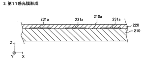
- a first photosensitive film is formed on the upper surface of the piezoelectric material layer (see the photosensitive film forming step (c1)).
- the first exposure step (c2) light is irradiated from the second main surface side of the substrate facing the first main surface toward the substrate (first main surface).
- the irradiation direction of this light is parallel to the direction orthogonal to the first main surface.
- the hollow portion may be filled with a substance containing a light shielding material.
- the cavity is filled with a substance containing a light-shielding material, and a photosensitive film (referred to as a “third photosensitive film” for convenience) is formed on the upper surface of the substrate.
- a photosensitive film referred to as a “third photosensitive film” for convenience
- the cavity portion is exposed without exposing the third photosensitive film existing inside the cavity projection region by irradiating the substrate with light parallel to the first principal surface orthogonal direction from the second principal surface side.
- a mask (referred to as “third mask” for convenience) is formed on the upper surface of the substrate by removing the unexposed third photosensitive film, Forming a conductive material film to be the first electrode on the upper surface of the first main surface of the substrate where the third mask does not exist; Thereafter, the third mask may be removed, thereby forming a conductive material film to be the first electrode inside the cavity projection region.
- the cavity is filled with a substance containing a light-shielding material, and the first projection is made in the cavity projection region by the above-described method.
- a conductive material film to be an electrode may be formed.
- the light irradiated on the substrate from the second main surface side cannot reach the inside of the cavity projection region due to the presence of the light shielding material and / or the conductive material film.
- the light irradiated from the second main surface side in the first exposure step (c2) can reach only the outside of the cavity projection region.
- the first exposure step (c2) is a step including these aspects. That is, in the first exposure step, the cavity is exposed without exposing the first photosensitive film existing inside the cavity projection area by light irradiated on the substrate from the second main surface side of the substrate. Exposing the first photosensitive film existing outside the partial projection area.
- the “position and shape in plan view (position and shape when viewed along the direction orthogonal to the first principal surface)” of the unexposed portion of the first photosensitive film is the position in plan view of the cavity. And the shape coincide with each other with extremely high accuracy.
- the exposed first photosensitive film portion is removed, and the unexposed first photosensitive film portion remains as a first mask.
- the position and shape of the first mask in plan view coincide with the position and shape of the cavity in plan view, respectively, with extremely high accuracy.
- a projection material containing at least one of abrasive grains and an organic solvent is projected toward the first main surface of the substrate.
- the piezoelectric material layer present in the portion where the first mask does not exist is removed, and the portion of the piezoelectric material layer covered with the first mask remains.
- the position and shape of the first mask in plan view coincide with the position and shape of the cavity in plan view, respectively, with extremely high accuracy. Therefore, the piezoelectric material layer is formed such that the position and shape in plan view coincide with the position and shape of the cavity in plan view, respectively.
- the piezoelectric material layer is formed with high precision so as to exist only in the region inside the cavity projection region above the first main surface of the substrate.
- the existence area of the piezoelectric element can be made to coincide with the “upper surface of the substrate and the cavity projection area” with high accuracy.
- the object to be processed in the piezoelectric material layer processing step (d) is a piezoelectric material layer (for example, a ceramic green sheet) before firing. Since the piezoelectric material layer before firing has a lower hardness than the piezoelectric material layer after firing, it is removed in a short time by the projection of the projection material. As a result, the time of the piezoelectric material layer processing step (d) can be shortened.
- One aspect of this production method is: (G) a second mask forming step; (H) a second mask removing step; Including.
- the second mask formation step (g) is performed after the substrate preparation step (a) and before the piezoelectric material layer formation step (b).
- the second mask formation step (g) Forming a second photosensitive film above the first main surface of the substrate; The cavity portion is exposed without exposing the second photosensitive film existing in the cavity projection region by irradiating the substrate with light parallel to the first principal surface orthogonal direction from the second principal surface side. Exposing the second photosensitive film present outside the projection area; Next, a second mask is formed above the substrate by removing the unexposed second photosensitive film.
- the exposure of the second photosensitive film is the same as the first exposure step (c2).
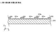
- the second mask removing step (h) is performed after the piezoelectric material layer processing step (d).
- the second mask removing step (h) is a step of removing the second mask.
- the position and shape of the second mask in plan view are extremely accurate with respect to the position and shape of the substrate in which the cavity portion is not formed (non-cavity portion) for the same reason as that for the first mask. Match well.
- the piezoelectric material layer is formed so as to cover the second mask.
- the second mask removing step (h) is performed after the piezoelectric material layer processing step (d)
- the removal rate of the piezoelectric material layer is small, such as when removing the piezoelectric material layer using abrasive grains having a small particle size, and when removing the piezoelectric material layer only with an organic solvent.
- This is particularly advantageous. That is, even when the removal rate (processing rate) of the piezoelectric material layer is low, the thickness of the piezoelectric material layer to be removed is small, so that the removal of the piezoelectric material layer can be completed within a relatively short time. . Therefore, it is possible to process the piezoelectric material layer in a short time while maintaining high processing accuracy of the piezoelectric material layer.
- the support forming step (i) is performed before the piezoelectric material layer processing step (d).
- the support forming step (i) is a step of forming a support in the cavity by filling the cavity with a fluid substance and curing the fluid substance.
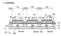
- the support removing step (j) is performed after the piezoelectric material layer processing step (d).
- the support removing step (j) is a step of removing the support (from the cavity).
- a projection material is projected.
- pressure is applied to the portion constituting the first main surface of the substrate.
- a part of the substrate constituting the cavity and the part constituting the first main surface that is, the boundary between the cavity and the piezoelectric element
- a part of the substrate constituting the cavity and the part constituting the first main surface that is, the boundary between the cavity and the piezoelectric element
- the above aspect addresses such problems. That is, according to the said aspect, a projection material is projected in the state in which the "hardened support body" was formed in the cavity part. As a result, it is possible to avoid the deformation or breakage of the boundary portion between the cavity and the piezoelectric element.
- the cavity is filled with a fluid substance containing a light-shielding material, and the fluid substance is cured, thereby supporting the light-shielding function in the cavity.
- the projection material is projected in a state where the “cured support” is formed in the cavity.
- the support forming step (k) is performed before the first exposure step (c2). Accordingly, when the light is irradiated from the second main surface side of the substrate toward the substrate in the first exposure step (c2), a cured body (mask) containing a light-shielding material is formed in the cavity. Existing. Accordingly, the accuracy of the position and shape of the first photosensitive film exposed in the first exposure step (c2) can be improved.
- the third mask formation step (m) is performed after the substrate preparation step (a) and before the piezoelectric material layer formation step (b).
- the third mask forming step (m) Filling the cavity with a substance containing a light-shielding material and forming a third photosensitive film above the first main surface of the substrate; The cavity portion is exposed without exposing the third photosensitive film existing inside the cavity projection region by irradiating the substrate with light parallel to the first principal surface orthogonal direction from the second principal surface side. Exposing the third photosensitive film present outside the projection area; Forming a third mask above the substrate by removing the unexposed third photosensitive film;
- the position and shape of the third mask formed by the third mask formation step (m) are the same as the reason for the first mask, and the portion of the substrate where the cavity portion is not formed (non-cavity portion).
- the position and shape in plan view coincide with each other with extremely high accuracy.
- the conductive material film forming step (n) is performed after the third mask forming step (m) and before the piezoelectric material layer forming step (b). Therefore, the conductive material film forming step (n) is performed before the first exposure step (c2).
- the conductive material film forming step (n) is a step of forming a conductive material film serving as the first electrode on the upper surface of the first main surface of the substrate where the third mask is not present. .
- the conductive material film to be the first electrode is formed along the third mask. Accordingly, the position and shape of the conductive material film can be matched with the position and shape of the hollow portion in plan view with extremely high accuracy.
- Such an aspect further includes A third mask removing step (o) for removing the third mask may be included after the conductive material film forming step (n) and before the piezoelectric material layer forming step (b).
- the first exposure step (c2) is a step of exposing the first photosensitive film while functioning the conductive material film as a mask.
- the position and shape of the conductive material film formed using the third mask coincide with the position and shape of the cavity in plan view, respectively, with extremely high accuracy. Therefore, when the substrate is irradiated with the light from the second main surface side of the substrate in the first exposure step (c2), exposure is performed by using the conductive material film as a “mask for blocking the light”. Thus, the accuracy of the position and shape of the first photosensitive film can be improved.
- the light-shielding material filled in the cavity in the third mask formation step (m) is used as a mask to function the first photosensitive film. It may be a step of exposing.
- the light-shielding material filled in the cavity used when forming the third mask for forming the conductive material film can be used as the mask in the first exposure step.
- the light irradiated in the first exposure step (c2) can be more reliably blocked by the light-shielding material filled in the hollow portion used when forming the conductive material film and the third mask, The accuracy of the position and shape of the first photosensitive film exposed by the light can be improved.
- the third mask formation step (m) includes forming a cured body that cures the fluid substance filled in the cavity before irradiation with light for exposing the third photosensitive film
- the piezoelectric material layer processing step (d) may be a step of projecting the projection material in a state where the cured body formed in the third mask formation step (m) is held in the cavity.
- the light-shielding material filled in the cavity used when forming the third mask for forming the conductive material film is used to project the projection material in the piezoelectric material layer processing step (d).
- it can be used as "a cured body that functions as a support that prevents deformation or breakage of the boundary". That is, the light shield used in the third mask formation step (m), the light shield used in the first exposure step (c2), and the piezoelectric material layer processing step (d). And the support can be formed in one step. Therefore, the manufacturing process can be simplified.
- the substance containing the light-shielding material filled in the cavity in the third mask forming step (m) is a fluid substance
- the fluid state filled in the cavity in the third mask forming step (m) Including a first cured body forming step of forming a first cured body by curing the material of
- the piezoelectric material layer processing step (d) may be a step of projecting the projection material in a state where the first cured body is held in the cavity.
- the light-shielding material filled in the cavity used when forming the third mask for forming the conductive material film is used to project the projection material in the piezoelectric material layer processing step (d).
- it can be used as "a cured body that functions as a support that prevents deformation or breakage of the boundary". That is, the light shielding material used in the third mask formation step (m), the light shielding material used in the first exposure step (c2), and the piezoelectric material layer processing step (d And the substance to be the support used in step 1) can be filled in the cavity by one step. Therefore, the manufacturing process can be simplified.
- the “light-shielding material in the cavity used in the third mask formation step” is removed from the cavity, and a different “light-shielding material” is refilled in the cavity before the first exposure step. May be implemented.
- the substance containing the light-shielding material refilled in the cavity in the light-shielding material refilling step (r) is a fluid substance
- the cavity is refilled in the light shielding material refilling step (r).
- the piezoelectric material layer processing step (d) is a step of projecting the projection material in a state where the second cured body is held in the cavity. Is preferred.
- the material in the cavity used as the mask in the first exposure step (c2) (the light-shielding material refilled in the cavity in the light-shielding material refilling step (r)) is piezoelectric. It can also be used as a support in the material layer processing step (d). That is, the substance serving as the light blocking body used in the first exposure step (c2) and the substance serving as the support used in the piezoelectric material layer processing step (d) are formed into the cavity by one step. Can be filled. Therefore, the manufacturing process can be simplified.
- the second mask forming step (t) is performed after the third mask removing step (o) and before the piezoelectric material layer forming step (b).
- the second mask forming step (t) Forming a second photosensitive film above the first main surface of the substrate;
- the substrate is irradiated with light parallel to the direction orthogonal to the first main surface from the second main surface side, and at least the conductive material film is used as a mask, so that the first existing in the cavity projection region is present. 2 exposing the second photosensitive film existing outside the cavity projection region without exposing the photosensitive film,
- a second mask is formed on the upper surface of the substrate by removing the unexposed second photosensitive film.
- the second mask removing step (u) is performed after the piezoelectric material layer processing step (d).
- the second mask removing step (u) is a step of removing the second mask.
- the position and shape of the second mask formed in the second mask formation step (t) in plan view are the same as the reason for the first mask, and the position and shape of the non-cavity portion of the substrate in plan view are the same. Each matches very accurately.
- the piezoelectric material layer is formed so as to cover the second mask.
- the second mask removal step (u) is performed after the piezoelectric material layer processing step (d)
- the second mask exists at the time of performing the piezoelectric material layer processing step (d). . Therefore, in the piezoelectric material layer processing step (d), the thickness of the piezoelectric material layer that must be removed by projecting the projection material is “thickness of the second mask” as compared with the case where the second mask is not formed. It becomes smaller by “minute”. As a result, the removal of the piezoelectric material layer can be completed in a short time.
- this manufacturing method (V) After the piezoelectric material layer forming step (b) and before the photosensitive film forming step (c1), the piezoelectric material layer and the first photosensitive film are in contact with the upper surface of the piezoelectric material layer.
- the reaction preventing layer existing outside the cavity projection region without removing the reaction preventing intermediate layer existing inside the cavity projection region It is desirable to include a reaction preventing intermediate layer removing step for removing the intermediate layer.
- the reaction preventing intermediate layer may be removed, for example, in the piezoelectric material layer processing step (g).
- the piezoelectric material layer and the first photosensitive film undergo a dissolution reaction, and a part of the piezoelectric material layer (upper part) and a part of the first photosensitive film (lower part).
- the first mask removing step (e) only the first mask cannot be removed, and even the piezoelectric material layer may be removed.
- a reaction preventing intermediate layer is formed above the piezoelectric material layer, and then a first photosensitive film is formed. According to this, since no dissolution reaction occurs between the piezoelectric material layer and the first photosensitive film, only the first mask can be easily removed in the first mask removing step (e).
- the substrate of the piezoelectric film type device manufactured by this manufacturing method can include a plurality of the hollow portions.
- the substrate preparation step (a) is a step of forming the substrate such that the plurality of cavities are arranged at a predetermined distance in a direction along the first main surface.
- the piezoelectric film type device including the piezoelectric film is accurately formed in the cavity projection region. Therefore, even when the substrate includes a plurality of cavities, the volume deformation characteristics between the cavities can be matched with each other. Therefore, the present manufacturing method is a piezoelectric film type device (for example, for inkjet) comprising a plurality of cavities and a plurality of piezoelectric elements each formed inside each cavity projection region of the plurality of cavities. It is preferably used when manufacturing an actuator.
- the baked piezoelectric element is processed by blasting.
- the fired piezoelectric element has a high hardness. Therefore, there is a problem that the time required for blasting becomes long. Therefore, in order to shorten the time required for blasting, it is conceivable to use abrasive grains having a large grain size. However, if the grain size of the abrasive grains is large, fine processing becomes difficult. Therefore, when the substrate includes a plurality of cavities and the distance between adjacent cavities is short, abrasive grains having a large particle diameter cannot be used. Therefore, the blasting time becomes long.
- each aspect of the present invention removes the piezoelectric material layer before firing in the piezoelectric material layer processing step (d).
- the piezoelectric material layer before firing has a lower hardness than the piezoelectric material layer after firing. Therefore, when the grain size of the abrasive grains is small or when the piezoelectric material layer is removed only with the organic solvent, the time of the piezoelectric material layer processing step (d) can be shortened. As a result, each aspect of the present invention can efficiently manufacture a piezoelectric film type device having a fine pattern such as a short distance between cavities.
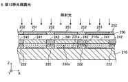
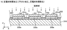
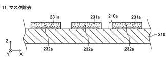
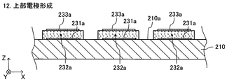
- FIG. 1 is a schematic perspective view of a piezoelectric film type device manufactured by a manufacturing method (first manufacturing method) of a piezoelectric film type device according to a first embodiment of the present invention.
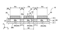
- 2 is a cross-sectional view of the piezoelectric film type device obtained by cutting the piezoelectric film type device shown in FIG. 1 along a plane along line 1-1 in FIG.
- 3 is a sectional view of the piezoelectric film type device obtained by cutting the piezoelectric film type device shown in FIG. 1 along a plane along line 2-2 in FIG.
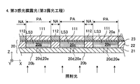
- FIG. 4 is a diagram for explaining a first step of the first manufacturing method.
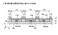
- FIG. 5 is a diagram for explaining a second step of the first manufacturing method.
- FIG. 1 is a schematic perspective view of a piezoelectric film type device manufactured by a manufacturing method (first manufacturing method) of a piezoelectric film type device according to a first embodiment of the present invention.
- 2 is a cross-sectional view of the piezo
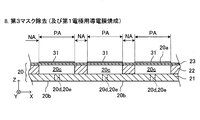
- FIG. 6 is a diagram for explaining a third step of the first manufacturing method.
- FIG. 7 is a diagram for explaining a fourth step of the first manufacturing method.
- FIG. 8 is a diagram for explaining a fifth step of the first manufacturing method.
- FIG. 9 is a diagram for explaining a sixth step of the first manufacturing method.
- FIG. 10 is a diagram for explaining a seventh step of the first manufacturing method.
- FIG. 11 is a diagram for explaining an eighth step of the first manufacturing method.
- FIG. 12 is a diagram for explaining a ninth step of the first manufacturing method.
- FIG. 13 is a diagram for explaining a tenth step of the first manufacturing method.
- FIG. 14 is a diagram for explaining an eleventh step of the first manufacturing method.
- FIG. 13 is a diagram for explaining a tenth step of the first manufacturing method.
- FIG. 15 is a diagram for explaining a twelfth process of the first manufacturing method.
- FIG. 16 is a diagram for explaining a thirteenth step of the first manufacturing method.
- FIG. 17 is a diagram for explaining a fourteenth step of the first manufacturing method.
- FIG. 18 is a diagram for explaining a fifteenth step of the first manufacturing method.
- FIG. 19 is a diagram for explaining a sixteenth step of the first manufacturing method.
- FIG. 20 is a diagram for explaining a seventeenth step of the first manufacturing method.
- FIG. 21 is a diagram for explaining an eighteenth step of the first manufacturing method.
- FIG. 22 is a diagram for explaining a nineteenth process of the first manufacturing method.
- FIG. 23 is a diagram for explaining other steps of the first manufacturing method.
- FIG. 16 is a diagram for explaining a thirteenth step of the first manufacturing method.
- FIG. 17 is a diagram for explaining a fourteenth step of the first manufacturing method.
- FIG. 18 is a diagram for explaining a fifteen
- FIG. 24 is a graph showing processing rates of Examples and Comparative Examples manufactured by the first manufacturing method.
- FIG. 25 is a diagram for explaining a first step of a piezoelectric film type device manufacturing method (second manufacturing method) according to the second embodiment of the present invention.
- FIG. 26 is a diagram for explaining a second step of the second manufacturing method.
- FIG. 27 is a diagram for explaining a third step of the second manufacturing method.
- FIG. 28 is a diagram for explaining a fourth step of the second manufacturing method.
- FIG. 29 is a diagram for explaining a fifth step of the second manufacturing method.
- FIG. 30 is a diagram for explaining a sixth step of the second manufacturing method.
- FIG. 31 is a diagram for explaining a seventh step of the second manufacturing method.
- FIG. 25 is a diagram for explaining a first step of a piezoelectric film type device manufacturing method (second manufacturing method) according to the second embodiment of the present invention.
- FIG. 26 is a diagram for explaining a second step of the second manufacturing method.
- FIG. 32 is a diagram for explaining an eighth step of the second manufacturing method.
- FIG. 33 is a diagram for explaining a ninth step of the second manufacturing method.
- FIG. 34 is a diagram for explaining a tenth process of the second manufacturing method.
- FIG. 35 is a diagram for explaining an eleventh step of the second manufacturing method.
- FIG. 36 is a diagram for explaining a twelfth process of the second manufacturing method.
- ⁇ First Embodiment> 1 to 3 are schematic views of a piezoelectric film type device 10 manufactured by the manufacturing method according to the first embodiment of the present invention.
- the piezoelectric film type device 10 is, for example, an ink jet actuator used for a head of a printer device or the like.
- the piezoelectric film type device 10 is also used for other purposes.
- the piezoelectric film type device 10 includes a single substrate 20 and a plurality of piezoelectric elements 30.
- the manufacturing method according to each embodiment of the present invention can also be used when manufacturing a piezoelectric film type device 10 including one substrate and one piezoelectric element.
- the substrate 20 is a thin plate body having a rectangular parallelepiped shape having sides parallel to the X axis, the Y axis, and the Z axis orthogonal to each other.
- the substrate 20 includes a first main surface 20a parallel to the XY plane and a second main surface 20b parallel to the XY plane. That is, the first main surface 20a and the second main surface 20b are parallel to each other and face each other.
- the substrate 20 includes a plurality of cavities (cavities, hollow chambers) 20c.
- the shape of the hollow portion 20c is a shape having a side parallel to each of the X axis and the Y axis (such as a rectangular parallelepiped and a quadrangular pyramid). Therefore, the shape of the cavity 20c in plan view (the shape of the cavity 20c viewed from the direction parallel to the Z axis) is a rectangle.
- the size of the shape of the end portion on the second main surface 20b side is the first size.
- the shape of the hollow portion 20c is not limited as long as it is smaller than the size of the end portion on the one main surface 20a side.
- the positive Z-axis direction is defined as “upward” for convenience
- the negative Z-axis direction is defined as “downward” for convenience
- “planar shape” or “shape in plan view” of a certain member or space or the like means that the member or space or the like is in a direction parallel to the Z axis (the first main surface 20a of the substrate 20).
- the direction orthogonal to the first main surface 20a of the substrate 20 is also referred to as a “first main surface orthogonal direction”.
- the plurality of hollow portions 20c have substantially the same shape and the same size.
- the length (width W1) in the short direction of the cavity 20c is preferably, for example, 30 ⁇ m or more and 200 ⁇ m or less.
- the length (width W2) in the longitudinal direction of the cavity 20c is preferably, for example, 0.5 mm or more and 3 mm or less.
- the height (H1) of the cavity 20c is preferably 10 ⁇ m or more and 300 ⁇ m or less, for example.
- the shape of the cavity 20c is not limited to a rectangular parallelepiped shape. That is, the planar shape of the hollow portion 20c may be a polygon other than a rectangle, a circle, an ellipse, a shape in which a part and all of the contour is a curve, or the like. Furthermore, the plurality of hollow portions 20c in this example have the same shape. However, the plurality of hollow portions 20c may have different shapes.
- the plurality of cavities 20c are arranged at a predetermined distance L1 in the X-axis direction as shown in FIG.
- the distance L1 is also referred to as an inter-cavity space (inter-cavity space) L1.
- the distance L1 is preferably 1 ⁇ m or more and 50 ⁇ m or less, and more preferably 3 ⁇ m or more and 20 ⁇ m or less.
- the plurality of inter-cavity spaces L1 may be the same or different from each other.
- the sides of the Y axis negative direction end portions of the plurality of hollow portions 20c are on one straight line parallel to the X axis. Accordingly, the side of each of the plurality of hollow portions 20c at the positive end in the Y-axis direction is on another straight line parallel to the X-axis.
- Each upper wall (a surface parallel to the XY plane at the end in the positive direction of the Z axis) of each of the plurality of cavities 20c exists in one plane parallel to the XY plane. Accordingly, the lower wall of each of the plurality of cavities 20c (the plane parallel to the XY plane at the end in the negative direction of the Z axis) exists in another plane parallel to the XY plane.
- the substrate 20 is a substrate in which the plurality of hollow portions 20c are arranged at a predetermined distance L1 in the direction along the first main surface 20a.
- the plurality of cavities 20c may be arranged in a lattice pattern or irregularly.
- a pair of communication passages 20d and 20e is connected to the hollow portion 20c.
- Each of the communication paths 20 d and 20 e communicates the cavity 20 c with the outside of the substrate 20.
- Each of the communication paths 20d and 20e has a cylindrical shape having an axis extending along the Z-axis direction.
- One end of the communication path 20d opens in the lower wall near the end in the Y-axis positive direction of the cavity 20c.
- the other end of the communication path 20d is open to the second main surface 20b of the substrate 20.
- One end of the communication path 20e opens in the lower wall near the end in the negative Y-axis direction of the cavity 20c.
- the other end of the communication path 20e opens to the second main surface 20b of the substrate 20.
- the shape of the through hole may be a shape other than a cylindrical shape (for example, a rectangular parallelepiped shape).
- one of the communication paths 20d and 20e has one end that forms an opening in a “wall that forms the cavity 20c and is parallel to the XZ plane”, and extends in the Y-axis direction. It may be a passage that communicates the outside of the substrate 20 with the cavity 20c. Further, the communication path extending in such an axial direction has a position where the other end does not overlap with the hollow portion 20c in a plan view (when the substrate 20 is viewed from the Z-axis direction). A passage that forms an opening in any one of the second main surfaces 20b may be used.
- the substrate 20 includes a lower plate (first base plate) 21, an intermediate plate (second base plate) 22, and a diaphragm 23.
- the lower plate 21, the intermediate plate 22, and the diaphragm 23 are made of an insulating ceramic.
- the lower plate 21, the intermediate plate 22, and the diaphragm 23 are laminated in order and integrated by firing. That is, the substrate 20 is a ceramic fired body.
- the insulating ceramic that is the material of the lower plate 21, the intermediate plate 22, and the diaphragm 23 is not particularly limited, but is selected from the group consisting of, for example, zirconium oxide, aluminum oxide, magnesium oxide, mullite, aluminum nitride, and silicon nitride. It is comprised from the material containing at least 1 type. In particular, stabilized zirconium oxide and partially stabilized zirconium oxide are preferable as the material of the substrate 20 from the viewpoint of mechanical strength and toughness.
- the lower plate 21 is a thin plate body having a substantially uniform thickness.
- the lower plate 21 is formed with a plurality of through-holes arranged at predetermined positions and forming the above-described communication paths 20d and 20e.
- the upper surface of the lower plate 21 constitutes the lower wall surface of the cavity 20c.
- the intermediate plate 22 is a thin plate body having a substantially uniform thickness H1.
- the intermediate plate 22 is formed with a plurality of through holes arranged at predetermined positions. The side wall surface of this through hole constitutes the side wall surface of the cavity 20c.
- the diaphragm 23 is a thin plate having a substantially uniform thickness.
- the thickness of the diaphragm 23 is, for example, preferably 30 ⁇ m or less, and more preferably 1 ⁇ m or more and 15 ⁇ m or less.
- the lower surface of the diaphragm 23 constitutes the upper wall surface of the cavity 20c.
- the diaphragm 23 is deformed as the piezoelectric element 30 expands and contracts.
- the upper surface of the diaphragm 23 is the first main surface 20 a of the substrate 20.
- the total thickness of the lower plate 21, the intermediate plate 22, and the vibration plate 23 (that is, the thickness of the substrate 20) is determined so that “light for exposure” to be described later can sufficiently pass through the substrate 20. Is done. “Light for exposure” is light that travels from the second main surface 20b to the first main surface 20a and is parallel to the first main surface orthogonal direction (Z-axis direction). Hereinafter, “light for exposure” is also referred to as “irradiation light”. Whether or not the irradiation light can be sufficiently transmitted through the substrate 20 also varies depending on the material and density of the substrate 20.
- the total thickness of the lower plate 21 and the intermediate plate 22 is preferably 20 ⁇ m or more and 300 ⁇ m or less. Therefore, the thickness of the substrate 20 is preferably 21 ⁇ m or more and 330 ⁇ m or less.
- the piezoelectric element 30 includes a first electrode (lower electrode film, lower electrode layer) 31, a piezoelectric film 32, and a second electrode (upper electrode film, upper electrode layer).
- the first electrode 31 is a fired body (sintered body) of a conductive material.
- the first electrode 31 is formed of, for example, a metal such as platinum, palladium, rhodium, gold, and silver, or an alloy containing these metals as a main component.
- the first electrode 31 may be formed from another conductive material.
- the thickness of the first electrode 31 is preferably about 0.3 to 5.0 ⁇ m after sintering, for example. However, the thickness and material of the first electrode 31 need to be determined together with the thickness and material of the diaphragm 23 so as not to transmit “irradiation light”.
- an image obtained by projecting the cavity 20 c in the direction orthogonal to the first principal surface” with respect to the first principal surface 20 a of the substrate 20 is referred to as a “cavity projection image”.
- the “space area PA formed by extending the cavity projection image in the direction orthogonal to the first main surface” is referred to as “cavity projection area PA”. Therefore, the cavity projection area PA coincides with the cavity 20c in plan view. That is, in the plan view, the contour of the cavity projection area PA matches the “contour of the cavity 20 c” and the “contour of the cavity projection image”.
- the first electrode 31 is disposed (formed) on (upper surface) the first main surface 20a of the substrate 20. Further, the first electrode 31 is formed so as to exist in (inside) the cavity projection area PA. In other words, the first electrode 31 is provided so that “the position and shape of the first electrode 31 in plan view coincide with the position and shape of the cavity 20 c in plan view”.
- the first electrode 31 is integrated with the diaphragm 23.
- a lower wiring electrode (not shown) is connected to the first electrode 31.
- the lower wiring electrode is connected to a drive circuit (not shown) and constitutes a power feeding path to the first electrode 31.
- the piezoelectric film 32 is a sintered body of piezoelectric ceramic.
- the material of the piezoelectric film 32 is not particularly limited, and examples thereof include lead (Pb) -based perovskite oxide and non-lead-based perovskite oxide from the viewpoint of electric field induced strain.
- Lead (Pb) -based perovskite oxide is lead zirconate titanate (PZT; Pb (Zr x Ti 1-x ) O 3 ) or “zirconate titanate into which a simple oxide and / or a composite perovskite oxide is introduced. More preferably, it is a modified product of lead acid.
- the following materials can be used as the material of the piezoelectric film 32.
- Lead zirconate titanate PZT; Pb (Zr x Ti 1-x ) O 3 ).
- Solid solution of lead zirconate titanate and lead niobate niobate Pb (Ni 1/3 Nb 2/3 ) O 3 ).
- As the lead-free perovskite oxide (Na, Nb) TiO 3 , (K, Nb) TiO 3 , (Bi, Na) TiO 3 , BaTiO 3 , SrTiO 3 , and the like.
- the thickness of the piezoelectric film 32 is, for example, preferably 1 ⁇ m or more and 15 ⁇ m or less after firing, and more preferably 1 ⁇ m or more and 5 ⁇ m or less.
- the piezoelectric film 32 is subjected to polarization processing.
- the piezoelectric film 32 is disposed (formed) on the first electrode 31 (upper surface). Furthermore, the piezoelectric film 32 is formed so as to exist in (inside) the cavity projection area PA. In other words, the piezoelectric film 32 is provided so that “the position and shape of the piezoelectric film 32 in plan view coincide with the position and shape of the cavity 20 c in plan view”.
- the piezoelectric film 32 is integrated with the first electrode 31. Therefore, the distance between the adjacent piezoelectric films 32 (the space between the piezoelectric films) is substantially equal to the space L1 between the cavity portions. Therefore, the space between the piezoelectric films is preferably 1 ⁇ m or more and 50 ⁇ m or less, and more preferably 3 ⁇ m or more and 20 ⁇ m or less.
- the second electrode 33 is a metal sintered body made of the same material as the first electrode 31.
- the thickness of the second electrode 33 is preferably, for example, about 0.06 to 3.0 ⁇ m after sintering.
- the second electrode 33 is disposed (formed) on the piezoelectric film 32 (upper surface). Further, the second electrode 33 is formed so as to exist in (inside) the cavity projection area PA. In other words, the second electrode 33 is provided so that “the position and shape of the second electrode 33 in plan view coincide with the position and shape of the cavity 20 c in plan view”.
- the second electrode 33 is integrated with the piezoelectric film 32. Therefore, the piezoelectric element 30 is integrated with the vibration plate 23 (accordingly, the substrate 20).
- An upper wiring electrode (not shown) is connected to the second electrode 33. The upper wiring electrode is connected to the drive circuit (not shown) and constitutes a power feeding path to the second electrode 33.
- the piezoelectric film device 10 when a varying potential difference is applied between the first electrode 31 and the second electrode 33 (that is, when a varying voltage is applied to the piezoelectric film 32), the piezoelectric film device 10 is piezoelectric. A changing electric field is applied to the body film 32. As a result, the piezoelectric film 32 expands and contracts in a direction parallel to the first main surface 20a, and the diaphragm 23 integrated with the piezoelectric element 30 performs a bending motion. The volume of the cavity 20c changes with the bending movement of the diaphragm 23. Therefore, when the cavity 20c is filled with ink, the ink is ejected to the outside of the piezoelectric film type device 10 through the communication path 20d. The ink is introduced into the cavity 20c through the communication path 20e.
- first manufacturing method piezoelectric film type device manufacturing method
- First step First, the substrate 20 shown in FIG. 4 is created (prepared).
- substrate 20 is produced as follows, for example.
- a ceramic green sheet to be the lower plate 21 is prepared, and through holes to be the communication paths 20d and 20e are formed at positions corresponding to the communication paths 20d and 20e.
- a ceramic green sheet to be the intermediate plate 22 is prepared, and a through hole to be the cavity 20c is formed at a position corresponding to the cavity 20c.
- a ceramic green sheet to be the intermediate plate 22 is laminated on the ceramic green sheet to be the lower plate 21, and further a ceramic green sheet to be the vibration plate 23 is laminated on the ceramic green sheet to be the intermediate plate 22.
- the plates align with each other in the planar direction.
- the laminated ceramic green sheets are thermocompression bonded.
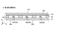
- a photoresist film 110 is formed on the upper surface of the first main surface 20 a of the substrate 20.
- This photoresist film 110 is referred to as a “third photosensitive film 110” for convenience.
- the third photosensitive film 110 is formed so as to cover the entire surface of the first main surface 20a.
- the third photosensitive film 110 may be applied by any method such as spin coating, slit coating, roll coating, spraying, and screen printing. Further, the third photosensitive film 110 may be formed by attaching a photosensitive dry film resist.
- the thickness of the third photosensitive film 110 is sufficiently larger than the thickness of the first electrode 31.
- the third photosensitive film 110 is a “negative type” photoresist whose solubility in a developer (organic solvent) decreases when exposed.
- membrane 110 is not specifically limited, For example, they are photosensitive resins, such as an acrylic type, an epoxy type, a polyimide type, and a fluorine type. Further, the material of the third photosensitive film 110 may be a chemical resistant protective agent. From the viewpoint of resolution during pattern formation, the third photosensitive film 110 is more preferably a film made of a chemically amplified photoresist.
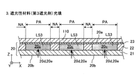
- the hollow portion 20c of the substrate 20 is filled with a fluid substance (liquid substance, third light-shielding agent LS3) containing a light-shielding material.
- the third light shielding agent LS3 is a light shielding liquid obtained by dissolving a solid light shielding agent in a solvent, or a light shielding liquid obtained by dispersing a solid light shielding agent in a dispersion medium.
- the light-shielding agent preferably contains a dye or pigment that absorbs light.
- the light shielding agent may have a refractive index different from that of the substrate 20. In this case, since “irradiation light” is totally reflected in the cavity 20c, the irradiation light cannot be transmitted through the cavity 20c.
- the light shielding liquid is filled into the cavity 20c by being injected into the cavity 20c by a syringe or the like through the communication path 20d and / or the communication path 20e. Thereafter, the substrate 20 is heated by a heating device such as a hot plate and an oven, thereby eliminating the “solvent or dispersion medium” of the third light shielding agent LS3. Thereby, the hardened light-shielding agent (light-shielding body) is formed in the cavity 20c.
- the hollow portion 20c may be filled with a “solid or semi-solid” “substance containing a light shielding material”. Furthermore, when the fluid substance containing the light-shielding material can be held in the cavity 20c in an uncured state, the fluid substance need not be cured.
- Fourth step (third photosensitive film exposure step, third exposure step) Next, as shown in FIG. 7, “light traveling from the second main surface 20 b side of the substrate 20 toward the first main surface 20 a and parallel to the first main surface orthogonal direction (Z-axis positive direction). ) ”Is applied to the substrate 20.
- the irradiated light (irradiated light) can pass through the portion of the substrate 20 where the cavity 20c is not formed, but cannot pass through the cavity 20c filled with the third light shielding agent LS3.
- the third photosensitive film 110 existing in (inside) the cavity projection area PA is not exposed and exists in the area NA other than the cavity projection area PA (external area NA of the cavity projection area PA). Only the third photosensitive film 110 is exposed.
- the exposed portion of the third photosensitive film 110 is also referred to as a post-exposure third photosensitive film 112.
- the “position and shape in plan view” of the non-exposed portion 111 of the third photosensitive film 110 coincides with the position and shape in plan view of the cavity 20c with extremely high accuracy.
- the non-exposed portion 111 of the third photosensitive film 110 is also referred to as a third photosensitive film non-exposed portion 111. Further, this step is also referred to as “third photosensitive film exposure step” or “third exposure step” for convenience.
- a conductive material film 31 a (first electrode 31 that becomes the first electrode 31) is formed on the upper surface of the first main surface 20 a of the substrate 20 where the third mask 112 does not exist. Electrode conductive film 31a) "is formed. Since the third mask 112 is removed later, the first electrode conductive film 31 a may also be formed on the upper surface of the third mask 112.
- the first electrode conductive film 31a can be formed, for example, by any one of the following methods (1) to (3).
- a paste in which a conductive material is dispersed in a dispersion medium (hereinafter also referred to as “conductive paste”) is applied by a screen printing method or the like. Next, the dispersion medium in the applied conductive paste is removed by evaporation.
- a solution in which a resinate of a conductive material is dissolved in a solvent hereinafter also referred to as “conductive resinate” is applied by a spin coating method, a spraying method, or the like. The solvent in the applied conductive resinate is then removed by evaporation.
- a conductive material is vapor-deposited on the upper surface of the first main surface 20a by a sputtering vapor deposition method, a resistance heating vapor deposition method, or the like.
- a conductive material is formed on the upper surface of the first major surface 20a by electroless plating.
- the third mask 112 is removed by peeling.
- the third mask 112 is peeled off by, for example, a chemical method, a heat treatment method, a plasma treatment method, or the like.
- the first electrode conductive film 31a is formed only on the upper surface of the first main surface 20a and in the cavity projection region PA.
- the position and shape of the portion where the third mask 112 does not exist in plan view coincide with the position and shape of the cavity 20c in plan view with extremely high accuracy. Therefore, the position and shape of the first electrode conductive film 31a in plan view coincide with the position and shape of the cavity 20c in plan view, respectively, with extremely high accuracy.
- the first electrode conductive film 31 a is baked to form the first electrode 31.
- a photoresist film 120 is formed above the first main surface 20 a of the substrate 20.
- This photoresist film 120 is referred to as “second photosensitive film 120” for convenience. That is, in this step, the second photosensitive film 120 is formed in a film shape on the exposed first main surface 20a and the first electrode 31.
- the method for applying the second photosensitive film 120 may be any of spin coating, slit coating, roll coating, spraying, screen printing, and the like. Further, the second photosensitive film 120 may be formed by attaching a photosensitive dry film resist.
- the second photosensitive film 120 is a “negative photoresist” whose solubility in a developing solution (alkaline aqueous solution or organic solvent) decreases when exposed.
- the material of the second photosensitive film 120 is not particularly limited, and is, for example, “photosensitive resin or photosensitive chemical-resistant protective agent” such as acrylic, epoxy, polyimide, and fluorine. From the viewpoint of resolution during pattern formation, the second photosensitive film 120 is more preferably a film made of a chemically amplified photoresist.
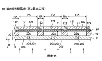
- the position and shape of the first electrode 31 in plan view coincide with the position and shape of the cavity 20c in plan view, respectively, with extremely high accuracy. Therefore, the second photosensitive film 120 existing in (inside) the cavity projection area PA is not exposed, and only the second photosensitive film 120 existing in the area NA other than the cavity projection area PA is exposed.
- the exposed portion of the second photosensitive film 120 is also referred to as a post-exposure second photosensitive film 122.
- the “position and shape in plan view” of the portion 121 of the second photosensitive film 120 that is not exposed coincides with the position and shape in plan view of the cavity 20 c with extremely high accuracy.
- a portion 121 of the second photosensitive film 120 that is not exposed is also referred to as a second photosensitive film non-exposed portion 121. Further, this step is also referred to as “second photosensitive film exposure step” or “second exposure step” for convenience.
- the second mask 122 may be heated by heating the entire substrate 20 using a hot plate, and the second mask 122 may be further cured.
- the thickness of the second mask 122 is the thickness of the first mask 131 (see FIG. 18) described later, and the processing selectivity of the piezoelectric material layer processing step (blast processing, see FIG. 20) described later. Is determined in consideration of For example, the thickness of the second mask 122 is preferably 2 ⁇ m or more and 10 ⁇ m or less, and more preferably 3 ⁇ m or more and 5 ⁇ m or less.
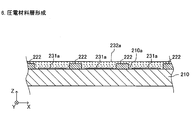
- the piezoelectric material layer 32 a is formed above the first main surface 20 a of the substrate 20. More specifically, the piezoelectric material layer 32a is formed by applying a piezoelectric ceramic paste to the upper surfaces of the “first electrode 31 and the second mask 122”.
- the method for applying the piezoelectric ceramic paste is not particularly limited. For example, wet coating such as spin coating, slit coating, roll coating, sol-gel method, spraying method and screen printing method, and electrophoresis using the lower electrode pattern as an electrode. Any of the methods can be suitably used.
- the piezoelectric material layer 32a may be formed by using a method such as ion beam, sputtering, vacuum deposition, PVD, ion plating, and CVD instead of applying the ceramic paste.
- the piezoelectric ceramic paste preferably has a solid content of 88 to 99% by weight, and more preferably has a solid content of 90 to 96% by weight from the viewpoint of sintering density and workability (pattern workability).
- the type of resin used as the binder of the piezoelectric ceramic paste is not particularly limited, but from the viewpoint of adsorption and dispersibility with the ceramic material, it is any one of butyral resin, cellulose resin and acrylic resin, or a mixture thereof. Is preferred.
- Step 12A reaction prevention intermediate layer forming step
- a reaction preventing intermediate layer HB is formed above (upper surface) the piezoelectric material layer 32a.
- the piezoelectric material layer 32a and the first photosensitive film 130 formed above the piezoelectric material layer 32a cause a dissolution reaction. It is a film to prevent it.
- the material of the reaction preventing intermediate layer HB is a material that prevents the material of the piezoelectric material layer 32a (the material of the piezoelectric film 32) and the first photosensitive film 130 from dissolving with each other. The material is not particularly limited as long as the material does not dissolve or react.
- the intermediate layer for reaction prevention HB for example, PVA (polyvinyl alcohol) and PAc (polyacrylic acid) which are hydrophilic resins are suitable.
- the method for applying the reaction preventing intermediate layer HB may be, for example, any one of spin coating, slit coating, roll coating, spraying, and screen printing.
- the film thickness of the reaction preventing intermediate layer HB is preferably 0.1 ⁇ m or more and 1 ⁇ m or less, and more preferably 0.5 ⁇ m.
- the reaction preventing intermediate layer forming step may be performed as necessary.
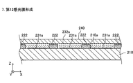
- 13th step Next, as shown in FIG. 16, above the piezoelectric material layer 32a (the upper surface of the piezoelectric material layer 32a when there is no reaction preventing intermediate layer HB, the reaction preventing medium when there is a reaction preventing intermediate layer HB).
- a photoresist film 130 is formed on the upper surface of the intermediate layer HB. This photoresist film 130 is referred to as a “first photosensitive film 130” for convenience.
- the first photosensitive film 130 is formed so as to cover the entire surface of the piezoelectric material layer 32a.
- the first photosensitive film 130 is preferably formed above the piezoelectric material layer 32a by attaching a photosensitive resin sheet.
- the first photosensitive film 130 may be applied by any one of spin coating, slit coating, roll coating, spraying, screen printing, and the like.
- the first photosensitive film 130 may be formed by attaching a photosensitive dry film resist.
- the first photosensitive film 130 is a “positive type” photoresist whose solubility in a developing solution (alkaline aqueous solution or organic solvent) increases when exposed.
- the material of the first photosensitive film 110 is not particularly limited, but is, for example, a rubber-based, urethane-based, epoxy-based, polyimide-based, or fluorine-based “photosensitive resin or photosensitive chemical-resistant protective agent”.
- first photosensitive film exposure step First exposure step
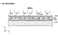
- first exposure step Next, as shown in FIG. 17, “light traveling from the second main surface 20 b side of the substrate 20 toward the first main surface 20 a and parallel to the direction orthogonal to the first main surface (Z-axis positive direction). ) ".
- the irradiated light irradiated light
- the position and shape of the first electrode 31 in plan view coincide with the position and shape of the cavity 20c in plan view, respectively, with extremely high accuracy. Accordingly, the first photosensitive film 130 existing in (inside) the cavity projection area PA is not exposed, and only the first photosensitive film 130 existing in the area NA other than the cavity projection area PA is exposed.
- the exposed portion of the first photosensitive film 130 is also referred to as a post-exposure first photosensitive film 132.
- the “position and shape in plan view” of the non-exposed portion 131 of the first photosensitive film 130 coincides with the position and shape in plan view of the cavity 20 c with extremely high accuracy.
- a portion 131 of the first photosensitive film 130 that is not exposed is also referred to as a first photosensitive film non-exposed portion 131. Further, this process is also referred to as “first photosensitive film exposure process” or “first exposure process” for convenience.
- a light blocking body may be formed in the cavity 20c before the first exposure step (14th step).
- the first photosensitive film 130 existing in (inside) the cavity projection area PA is not exposed by the light shield, and only the first photosensitive film 130 existing in the area NA other than the cavity projection area PA is exposed. Is done.
- the first exposure process (14th process) is an exposure process that uses the substrate 20 as a mask for irradiation light. That is, in the first exposure process (14th process), the irradiation light is irradiated to the outside NA of the cavity projection area without exposing the first photosensitive film 130 existing inside the cavity projection area PA. In this step, the existing first photosensitive film 130 is exposed.
- first photosensitive film exposed portion removing step completion of first mask
- the “exposed portion 132 of the first photosensitive film 130” is removed using a developer (alkaline aqueous solution or organic solvent).
- a developer alkaline aqueous solution or organic solvent.
- the first mask 131 may be heated by heating the entire substrate 20 using a hot plate, thereby further curing the first mask 131.
- the reaction preventing intermediate layer HB is removed with warm water (liquid temperature 60 ° C.).
- the removal method is not particularly limited, such as spraying, dipping / rocking, showering, and the like. Further, the reaction preventing intermediate layer may be removed by spraying using an air brush. Further, the reaction preventing intermediate layer HB may be removed by blasting in a piezoelectric material layer processing step to be described later.
- the step of removing the reaction preventing intermediate layer HB is referred to as a reaction preventing intermediate layer removing step.
- the reaction preventing intermediate layer removing step is described as follows: “The reaction preventing intermediate layer existing in the external NA of the cavity projection region without removing the reaction preventing intermediate layer HB existing in the cavity projection region PA. This is a step of removing HB.
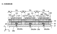
- the hollow portion 20c of the substrate 20 is filled with the fluid substance LS1.
- the fluid substance LS1 is heated after being filled in the cavity 20c, thereby drying and curing. That is, the fluid substance LS1 changes to a support SJ having a relatively high mechanical strength (see FIG. 20).
- the fluid substance LS1 is made of a material that can be removed from the cavity 20c by "heating, dissolution, ashing (ashing)" after drying and curing.
- a photoresist photosensitive resist
- wax hot melt, temporary adhesive, or the like
- a mixture in which a filler is mixed with a liquid can also be used as the fluid substance LS1.
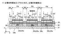
- the projection material is moved from the first main surface 20 a side to “the first main surface 20 a of the substrate 20 (actually, the upper surface of the piezoelectric material layer 32 a and the upper surface of the first mask 131. ) ". That is, blasting is performed. Thereby, the piezoelectric material layer 32a in a portion where the first mask 131 does not exist (portion not covered by the first mask 131) is removed. The portion of the piezoelectric material layer 32a covered with the first mask 131 is not removed.
- the projection material contains at least one of “abrasive grains and organic solvent”.
- the projection material is preferably a slurry containing an abrasive having a particle system of “0.1 ⁇ m or more and 5.0 ⁇ m or less”.
- the material of the abrasive ceramics having high Mohs hardness are preferable, and specifically, materials having a Mohs hardness of 11 or more such as silicon carbide, aluminum oxide, and zirconium oxide are preferable.
- the particle size of the abrasive contained in the projection material is more preferably 0.3 ⁇ m or more and 2.0 ⁇ m or less.
- the particle shape of the abrasive may be any of a polygonal shape, a spherical shape, a flat shape, and an indefinite shape.
- the solvent contained in the slurry is preferably water or an organic solvent. Furthermore, as a solvent contained in the slurry, from the viewpoint of workability of the piezoelectric material layer 32a (piezoelectric ceramics) and a film obtained by drying the piezoelectric ceramic paste (dry film), paste resin (for making the piezoelectric ceramic powder into a paste form) It is preferable to select an organic solvent having close compatibility (solubility parameter: Solubility parameter, SP value). Furthermore, the projection material may not contain an abrasive and may be only an organic solvent. In this case, the piezoelectric material layer 32a and the first mask 131 are removed by swelling and projection pressure.
- the projection material is projected by a “wet blasting device” or a “slurry spraying device”.
- the blast air pressure is preferably “0.05 Mpa or more and 0.5 Mpa or less”, and more preferably “0.15 Mpa or more and 0.25 Mpa or less”.
- the support SJ in the cavity 20c is removed.
- the support SJ is removed by a method according to the material of the support SJ (a method of removing by dissolving in an organic solvent, a method of removing by a chemical method, a method of removing by heating and burning, etc.). .
- the support SJ may be removed by a combination of these methods.
- first mask removing step and second mask removing step Next, the first mask 131 and the second mask 122 are removed (see FIG. 22). These masks are removed by a method according to the material (a method of removing by dissolving in an organic solvent, a method of removing by a chemical method, a method of removing by heating and burning, etc.). Further, these masks may be removed by a plasma ashing method, an organic matter cleaning method by excimer laser irradiation, or the like. These masks may be removed by a combination of these methods. Further, when the reaction preventing intermediate layer HB is formed, the reaction preventing intermediate layer HB is removed with warm water (liquid temperature 60 ° C.).
- the removal method is not particularly limited, such as spraying, dipping / rocking, showering, and the like. Further, the reaction preventing intermediate layer may be removed by spraying using an air brush. Thereafter, the piezoelectric material layer 32a is baked to form the piezoelectric film 32.
- the cavity is located above the first main surface 20a (the upper surface of the piezoelectric film 32 and the upper surface of the first main surface 20a), A mask (fourth mask) that exists in the region NA other than the projection region PA and does not exist in the cavity projection region PA is formed, and “the conductive material film 33a (second electrode 33 to be the second electrode 33) is formed using the mask. Electrode conductive film 33a) "is formed. The formation of the second electrode conductive film 33a is performed in the same manner as the formation of the first electrode conductive film 31a (see the seventh step). Then, the second electrode 33 is formed by firing the second electrode conductive film 33a. Next, a lower wiring electrode and an upper wiring electrode (not shown) are formed. Thus, the piezoelectric film type device 10 is manufactured.
- Piezoelectric material layer 32a Ceramic paste mainly composed of lead zirconate titanate (PZT) (PZT powder kneaded with resin binder and solvent into paste)
- the second mask 122 was formed according to the ninth to eleventh steps. Details are as follows. In the ninth step, formation (application) of the second photosensitive film (photosensitive negative resist film) 120 to be the second mask 122 was performed by spin coating. The rotation speed of the spin coat was 4500 rpm, and the holding time was 30 seconds. Thereafter, the second photosensitive film 120 was dried using a hot plate. The drying conditions were a drying temperature of 70 ° C. and a holding time of 10 minutes.
- irradiation light is irradiated from the second main surface 20b side toward the first main surface 20a using an exposure apparatus (three-line wavelength, lamp output 250W (high)), and the second photosensitivity.
- the latent image of the first electrode 31 was transferred to the film 120.
- the amount of light at this time was 300 mj / cm 2 .
- the substrate 20 on which the second photosensitive film 120 after exposure was formed was immersed in the developer and swung in the developer to form the second mask 122. Thereafter, in order to further cure the formed second mask 122, the substrate 20 on which the second mask 122 was formed was heat-treated with a hot plate.
- the heat treatment conditions were a drying temperature of 100 ° C. and a holding time of 3 minutes.
- the thickness (film thickness) of the second mask 122 was 8 ⁇ m (measured with a white interference type shape measuring instrument).
- the piezoelectric material layer 32a was formed (coated) by spin coating (rotation speed 3500 rpm, holding time 15 seconds) according to the twelfth step.
- the piezoelectric material layer 32 a was applied to the entire upper surface (including the upper surface of the first electrode 31) of the first main surface 20 a of the substrate 20. Thereafter, the piezoelectric material layer 32a was dried using a hot plate.
- the drying conditions were a drying temperature of 120 ° C. and a holding time of 5 minutes.
- the thickness (film thickness) after drying of the piezoelectric material layer 32a was 5 ⁇ m (measured with a white interference type shape measuring instrument).
- reaction preventing intermediate layer HB was formed as follows.
- a hydrophilic resin solution PVA (polyvinyl alcohol) having a concentration of 6% was applied to the entire upper surface of the piezoelectric material layer 32a by spin coating (the number of revolutions was 5000 rpm, holding time 15 seconds). -The solution was then dried using a hot plate. The drying conditions were a drying temperature of 150 ° C. and a holding time of 3 minutes.
- the reaction preventing intermediate layer HB was formed on the entire upper surface of the piezoelectric material layer 32a.
- the thickness (film thickness) of the reaction preventing intermediate layer HB was 0.5 ⁇ m (measured with a white interference type shape measuring instrument).
- the first mask 131 was formed according to the thirteenth to fifteenth steps. Details are as follows. In the thirteenth step, the first photosensitive film (photosensitive positive resist film) 130 to be the first mask 131 was formed by spin coating. The rotation speed of the spin coat was 2000 rpm, and the holding time was 15 seconds. Thereafter, the first photosensitive film 130 was dried on a hot plate. The drying conditions were a drying temperature of 100 ° C. and a holding time of 5 minutes. As a result, the first photosensitive film 130 was formed on the entire upper surface of the reaction preventing intermediate layer HB.
- irradiation light is irradiated from the second main surface 20b side toward the first main surface 20a by using an exposure apparatus (three-line wavelength, lamp output 250W (high)), and the first photosensitive
- the latent image of the first electrode 31 was transferred to the film 130.
- the light quantity at this time was set to 5000 mj / cm 2 .
- a sodium hydroxide aqueous solution (concentration 1%) was used as the developer used in the fifteenth step.
- the first mask 131 is formed by immersing the substrate 20 on which the exposed first photosensitive film 130 is formed in the developer and swinging the substrate 20 in the developer. Thereafter, in order to further cure the formed first mask 131, the substrate 20 on which the first mask 131 was formed was heat-treated with a hot plate.
- the heat treatment conditions were a drying temperature of 100 ° C. and a holding time of 3 minutes.
- the thickness (film thickness) of the first mask 131 was 5 ⁇ m (measured with a white interference type shape measuring instrument).
- the intermediate layer HB for preventing reaction was removed by spraying with warm water (liquid temperature 60 ° C.) using an air brush (time 1 minute).
- the shape of the reaction preventing intermediate layer HB after removal in the plan view is the same as the shape of the first mask 131 in the plan view.
- the formed reaction preventing intermediate layer HB was dried using a hot plate. The drying conditions were a drying temperature of 100 ° C. and a holding time of 5 minutes.
- Support SJ was prepared according to the sixteenth step.
- fluid photosensitive resin (fluid substance) LS1 was injected into the cavity 20c through the communication path 20d. Thereafter, using an exposure apparatus (three-line wavelength, lamp output 250 W (high)), irradiation light was irradiated from the second main surface 20b side toward the first main surface 20a to expose the photosensitive resin LS1.
- the fluid substance LS1 was cured to form the support SJ.
- the amount of light at this time was 300 mj / cm 2 .
- the substrate 20 on which the support SJ was formed was heat-treated with a hot plate. The heat treatment conditions were a drying temperature of 100 ° C. and a holding time of 10 minutes.
- Piezoelectric material layer removal The piezoelectric material layer 32a was removed (blasted) according to the seventeenth step. At this time, a micro wet blasting machine was used. The density
- the processing rate of the piezoelectric material layer 32a was calculated, and the integrated processing time required until the film thickness of the piezoelectric material layer 32a reached a desired value was obtained. Then, the above blasting was performed for the obtained integrated machining time.
- Support SJ was removed by the chemical method according to the eighteenth step.
- the “first mask 131 and second mask 122” were removed.
- the substrate 20 on which the piezoelectric material layer 32a and the like are formed is immersed in a sodium hydroxide aqueous solution (concentration 4%) as a resist stripping solution and is swung in the resist stripping solution.
- the “first mask 131 and the second mask 122” were removed.
- the reaction preventing intermediate layer HB was removed using warm water (liquid temperature 60 ° C.) or the like.
- the processing rate (processing speed of blast processing) of the piezoelectric film (piezoelectric material layer) 32a of the device manufactured according to the method described above was measured.
- the same blasting was performed on a sample obtained by firing the piezoelectric film (piezoelectric material layer) 32a.
- the solvent contained in the projection material was either “water or organic solvent”, and the processing rate was measured for samples having various gaps between the cavity portions. The measurement results are shown in FIG. Table 1 below describes the lines C1 to C3 in FIG.
- the abrasive grain contained in the projection material used the same abrasive grain in any projection material.
- the piezoelectric film that is the object of blasting is “ceramic green body before firing (after drying) as in the first manufacturing method”
- the piezoelectric body that is the object of blasting Compared with the case where the film is a “fired piezoelectric body (fired body)”, the processing rate is clearly improved.
- the piezoelectric film to be blasted is “ceramic green body before firing (after drying) as in the first manufacturing method”
- the solvent of the projection material is an organic solvent, the processing rate is remarkably high. growing.
- the piezoelectric film type device 10 for example, an inkjet actuator
- the piezoelectric film type device 10 having a very small space L1 between the cavity portions can be accurately and It was confirmed that it can be manufactured in a short time.
- the second mask 122 is formed.
- the second mask 122 may not be formed. That is, the ninth to eleventh steps may be omitted. In this case, only the first mask 131 is removed in the nineteenth step. In other words, the second mask removal step is omitted.
- the piezoelectric material layer processing step (17th step) is performed in a state where the support SJ is held in the cavity 20c.
- the support SJ may not be formed in the cavity 20c. Good.
- the support forming step (16th step) and the support removing step (18th step) are omitted.
- the support forming step (16th step) is performed after the first photosensitive film exposed portion removing step (15th step) and before the piezoelectric material layer processing step (17th step). It had been.
- the support forming process (the 16th process) may be performed before the piezoelectric material layer processing process (the 17th process). Therefore, for example, the support forming process (16th process) is performed before the first photosensitive film exposure portion removing process (15th process) (piezoelectric material layer forming process (12th process) and first photosensitive film forming process (first process). 13 process), and between the first photosensitive film forming process (13th process) and the first photosensitive film exposure process (14th process).
- first light shielding member / support forming step is a first exposure step (first step). It may be carried out before 14 steps).
- first light shielding and supporting body forming step is performed after the first photosensitive film forming step (13th step) and before the first exposure step (14th step).
- the second photosensitive film non-exposed portion removal may be performed after the piezoelectric material layer forming process (12th process) and before the first photosensitive film forming process (13th process). It may be performed after the step (11th step) and before the piezoelectric material layer forming step (12th step).
- the above-mentioned “fluid substance LS1 to be the support SJ” includes the light shielding material (the above-mentioned light shielding agent such as dye or pigment) in the cavity 20c.
- Such a fluid substance is a substance in which a light-shielding material is dispersed or dissolved in the fluid substance LS1.
- the fluid substance is cured by heating or the like.
- a “support having a light shielding function first light shielding body / support)” is formed in the cavity 20c.
- the projection material is projected in a state where the first light shielding body / support is formed in the cavity 20c.
- the boundary portion that is, the diaphragm 23
- the reaction preventing intermediate layer forming step may be performed after the piezoelectric material layer forming step (12th step) and before the first photosensitive film forming step (13th step). Further, in the reaction preventing intermediate layer forming step, when the material of the first photosensitive film is “a material with low solubility or a resin material with high hydrophilicity” (that is, the piezoelectric material layer 32a and the first material If it is difficult for the photosensitive film 130 to cause a dissolution reaction), it can be omitted.
- the first light shielding body / support forming step is performed before the first exposure step (14th step). Therefore, when the irradiation light is irradiated in the first exposure step (14th step), there is a cured body (mask: first light blocking body / support) containing a light blocking material in the cavity 20c. Will be. Therefore, the irradiation light is blocked by the light shielding body / support in the hollow portion 20 c in addition to the first electrode 31. As a result, it is possible to improve the accuracy of the position and shape of the portion of the first photosensitive film (first exposed photosensitive film 132 after exposure) exposed in the first exposure process (14th process). In addition, this 1st light shielding body and support body is removed in the said support body removal process (18th process).
- the third mask 112 is temporarily removed in the third mask removing step (eighth step), and then the second mask 122 is formed.
- the third mask 112 may be used as the second mask 122.
- the third mask removing step (eighth step) to the second photosensitive film non-exposed portion removing step (eleventh step) may be omitted.
- the light shielding agent LS3 is removed in the third light shielding agent removing step (sixth step).
- the third light shielding agent removing step (sixth step) can be performed after the first exposure step (fourteenth step) and before the support body forming step (sixteenth step).
- the second exposure step (tenth step) and the first exposure step (fourteenth step) are performed in a state where the light shielding agent LS3 is present in the cavity 20c.
- the shape accuracy (exposure accuracy) of the portion to be exposed in the second exposure step (tenth step) and the first exposure step (fourteenth step) can be improved.
- the first electrode 31 is made of a material that transmits the irradiation light and / or has a thickness that allows the first electrode 31 to transmit the irradiation light
- the second exposure is performed. The exposure of the process (10th process) and the first exposure process (14th process) can be performed reliably.
- the light shielding agent LS3 is removed in the third light shielding agent removing step (sixth step).
- the third light shielding agent removing step (sixth step) can be performed after the second exposure step (tenth step) and before the support body forming step (sixteenth step).
- the second exposure step (tenth step) is performed in a state where the light shielding agent LS3 is present in the cavity 20c.
- the shape accuracy (exposure accuracy) of the portion to be exposed in the second exposure step (tenth step) can be improved.
- the third mask removing step is performed before the second photosensitive film forming step (ninth step).
- the third mask removing step may be performed before the piezoelectric material layer forming step (twelfth step). That is, the third mask removing step (eighth step) is, for example, after the second photosensitive film forming step (ninth step) and before the second exposure step (tenth step), and the second exposure step (second step).
- the substance containing the light shielding material filled in the cavity 20c in the third light shielding agent filling step (third step) is a fluid substance, and further, the third light shielding agent filling step (third step) is performed. Further, it may include “curing the fluid substance filled in the cavity 20c (forming a cured body)” before irradiation with light for exposing the third photosensitive film 110.
- the third mask removing step is performed after the piezoelectric material layer processing step (17th step), and the piezoelectric material layer processing step (17th step) is the third light shielding agent filling step. It may be a step of projecting the projection material in a state where the hardened body formed in (third step) is held in the cavity 20c.
- the “light-shielding material filled in the cavity 20c” used when the “third mask 112 for forming the conductive material film 31a” is formed is processed by the piezoelectric material layer processing. It can be used as a support in the step (17th step) (a cured body that functions to prevent deformation or breakage of the diaphragm 23 when projecting the projection material). That is, the light shield used in the third mask formation step (actually, the third exposure step, which is the fourth step), the light shield used in the first exposure step (14th step), and the piezoelectric
- the support used in the material layer processing step (17th step) can be formed by one step (a third light shielding agent filling step which is the third step). Therefore, the manufacturing process can be simplified.
- the fluid substance filled in the cavity 20c was cured in the third light shielding agent filling step (third step).
- the third light shielding agent filling step In the third step, the “light-shielding material filled in the cavity 20c” is not cured, and is after the third photosensitive film non-exposed portion removing step (fifth step) and is processed with the piezoelectric material layer.
- the first cured body Prior to the step (17th step), the first cured body is formed by curing the fluid substance filled in the cavity 20c in the third light shielding agent filling step (third step).
- a forming step may be included.
- the piezoelectric material layer processing step (17th step) is a step of projecting the projection material in a state where the first cured body is held in the cavity.
- the material used as the light shielding body and the material used as the support used in the piezoelectric material layer processing step (17th step) are formed into the cavity portion by one third light shielding agent filling step (third step). 20c can be filled. Therefore, the manufacturing process can be simplified.
- the first cured body forming step may be performed after the third mask 112 is formed and before the first exposure step (14th step).
- the cavity 20c is filled.
- a light-shielding material refilling step of refilling a substance containing the light-shielding material may be included.
- the light-shielding material refilled in the cavity portion 20c in the light-shielding material refilling process functions as a mask. It may be a step of exposing the film 130.
- This light-shielding material refilling step is after the sixth step (third photosensitive film exposure material removal step, third light-shielding agent removal step) and before the second exposure step (tenth step). More preferably it is implemented. According to this, in the second exposure process, in addition to the conductive material film 31a, the second photosensitive film 120 is allowed to function as a mask with the light-shielding material refilled in the cavity 20c in the light-shielding material refilling process. Can be exposed.
- the substance containing the light-shielding material refilled in the cavity 20c can be used as a fluid substance.
- the fluid substance refilled in the cavity 20c in the light shielding material refilling step after the light shielding material refilling step and before the piezoelectric material layer processing step (17th step), the fluid substance refilled in the cavity 20c in the light shielding material refilling step.
- a second cured body forming step of forming a second cured body by curing can be included.
- the piezoelectric material layer processing step (17th step) is preferably a step of projecting the projection material in a state where the second hardened body is held in the hollow portion 20c.
- the material in the cavity 20c used as the mask for the irradiation light in the first exposure process (14th process) (refilled in the cavity 20c in the light-shielding material refilling process).
- the light shielding material) can also be used as a support in the piezoelectric material layer processing step (17th step). That is, the substance used as the light shielding body used in the first exposure process (14th process) and the substance used as the support used in the piezoelectric material layer processing process (17th process) are combined in one process.
- the hollow portion 20c can be filled. Therefore, the manufacturing process can be simplified.
- the second cured body forming step may be performed before the first exposure step (14th step).
- the first mask 131 and the second mask 122 are removed in one step with the same organic solvent.
- the first mask 131 and the second mask 122 may be removed in two or more steps. That is, the first mask 131 and the second mask 122 may be removed using different organic solvents or by different methods. In this case, as long as the process of removing the 1st mask 131 and the process of removing the 2nd mask are after the 17th process (piezoelectric material layer processing process), any may be performed first.
- the first manufacturing method and its modified examples are A method of manufacturing a piezoelectric film type device 10 comprising a substrate 20 and a piezoelectric element 30 having a piezoelectric film 32 and disposed on the first main surface 20a of the substrate, (A) a substrate preparation step for preparing the substrate (see FIG. 4); (B) Piezoelectric material layer forming step of forming a piezoelectric material layer 32a, which is a layer containing a piezoelectric material before firing that changes into the piezoelectric film by firing, above the first main surface 20a of the substrate (See FIG. 15) (C) a first mask creating step (see FIGS.
- a piezoelectric material layer processing step (see FIG. 20) to be removed;
- E a first mask removing step (see FIG. 22) for removing the first mask;
- F a firing step of firing the piezoelectric material layer; including.
- the piezoelectric material layer before firing is blasted in the piezoelectric material layer processing step. Therefore, blasting can be completed in a short time.
- a “piezoelectric film type device manufacturing method (hereinafter also referred to as“ second manufacturing method ”)” according to a second embodiment of the present invention will be described.
- the substrate of the piezoelectric film type device manufactured by the second manufacturing method is not provided with a cavity.
- a cavity may be provided in the substrate.
- First step First, the substrate 210 shown in FIG. 25 is created (prepared).
- the substrate 210 is produced, for example, by degreasing a plurality of ceramic green sheets laminated and thermocompression-bonded and then firing.
- a conductive material film 231 a (first electrode conductive film 231 a) to be a first electrode (lower electrode)” is formed on the first main surface 210 a of the substrate 210.
- the method for forming the conductive material film 231a is not particularly limited, but for example, it is preferably formed by any one of the following methods (1) to (3).
- a conductive paste is applied by a screen printing method or the like.
- the dispersion medium in the applied conductive paste is removed by evaporation.
- a conductive resinate is applied by a spin coating method, a spraying method, or the like. The solvent in the applied conductive resinate is then removed by evaporation.
- a conductive material is formed on the upper surface of the first main surface 210a by an electroless plating method.
- a photoresist film 220 is formed on the upper surface of the first main surface 210 a of the substrate 210.
- This photoresist film 220 is referred to as an “11th photosensitive film 220” for convenience.
- the eleventh photosensitive film 220 is formed to cover the entire surface of the first main surface 210a.
- the application method of the eleventh photosensitive film 220 may be any of spin coating, slit coating, roll coating, spraying, screen printing, and the like. Further, the eleventh photosensitive film 220 may be formed by attaching a photosensitive dry film resist.
- the thickness of the eleventh photosensitive film 220 is sufficiently larger than the thickness of the conductive material film 231a.
- the eleventh photosensitive film 220 is a “negative (negative type)” photoresist whose solubility in a developer (organic solvent) decreases when exposed, and the solubility in a developer (organic solvent) when exposed. Any of “positive type” photoresists in which the increase in the number of photoresists may be used.
- the eleventh photosensitive film 220 is composed of a negative photoresist.
- membrane 220 is not specifically limited, For example, they are photosensitive resins, such as an acryl type, an epoxy type, a polyimide type, and a fluorine type. Further, the material of the eleventh photosensitive film 220 may be a chemical resistant protective agent. From the viewpoint of resolution during pattern formation, the eleventh photosensitive film 220 is more preferably a film made of a chemically amplified photoresist.
- a mask 230 is disposed.
- the mask 230 is also referred to as an “eleventh mask 230” for convenience.
- the eleventh mask 230 is a quartz glass mask.
- the substrate of the eleventh mask 230 is a mask made of light transmissive quartz glass, and chromium (Cr) is deposited on the substrate.
- the portion where chromium is deposited constitutes a light shielding portion 231 that cannot transmit light, and the other portion constitutes a light transmitting portion 232.
- each light shielding portion 231 the main surface of the eleventh mask 230 is maintained parallel to the first main surface 210 a of the substrate 210, and the eleventh in the plane parallel to the main surface (in the XY plane).
- the mask 230 is formed so as to have a position and a shape covering each conductive material film 231a.
- Irradiated light can pass through the light transmission part 232 of the eleventh mask 230 but cannot pass through the light shielding part 231 of the eleventh mask 230.
- the eleventh photosensitive film 220 changes into an unexposed portion (non-exposed portion) 221 and an exposed portion (exposed portion) 222.
- the piezoelectric material layer 232 a is formed above the first main surface 210 a of the substrate 210. More specifically, the piezoelectric material layer 232a is formed by applying a piezoelectric ceramic paste to the upper surfaces of the “conductive material film 231a and the exposed portion 222”. There are no particular restrictions on the method of applying this piezoelectric ceramic paste, but for example, wet coating such as spin coating, slit coating, roll coating, sol-gel method, spraying method and screen printing method, and electric using the lower electrode pattern as an electrode. Any of the electrophoresis methods can be suitably used.
- the piezoelectric ceramic paste used in this step is the same as the piezoelectric ceramic paste used in the first manufacturing method.
- the piezoelectric material layer 232a may be formed by using a method such as ion beam, sputtering, vacuum evaporation, PVD, ion plating, and CVD instead of applying the ceramic paste.
- a reaction preventing intermediate layer HB (not shown) may be formed above (upper surface) of the piezoelectric material layer 232a.
- the piezoelectric material layer 232a and the twelfth photosensitive film 240 formed above the piezoelectric material layer 232a undergo a dissolution reaction. It is a film to prevent it.
- the material and forming method of the reaction preventing intermediate layer HB are the same as the material and forming method of the reaction preventing intermediate layer HB described in the first embodiment. Note that the reaction preventing intermediate layer forming step is not necessarily performed.
- a photoresist film 240 is formed on the upper surface of the intermediate layer HB.
- the photoresist film 240 is referred to as “a twelfth photosensitive film 240” or a “first photosensitive film” for convenience.
- the twelfth photosensitive film 240 is formed to cover the entire surface of the piezoelectric material layer 232a.
- the twelfth photosensitive film 240 is preferably formed above the piezoelectric material layer 232a by attaching a photosensitive resin sheet.
- the twelfth photosensitive film 240 may be applied by any method such as spin coating, slit coating, roll coating, spraying, and screen printing.
- the twelfth photosensitive film 240 may be either a positive type photoresist or a negative type photoresist.
- the twelfth photosensitive film 240 is composed of a positive photoresist.
- the material of the twelfth photosensitive film 240 is not particularly limited, and is, for example, a rubber-based, urethane-based, epoxy-based, polyimide-based, or fluorine-based “photosensitive resin or photosensitive chemical-resistant protective agent”.
- a mask 250 is disposed.
- the mask 250 is also referred to as “a twelfth mask 250” for convenience.
- the twelfth mask 250 is a quartz glass mask similar to the eleventh mask 230. Accordingly, the twelfth mask 250 includes a light shielding part 251 and a light transmission part 252. In each light shielding portion 251, the main surface of the twelfth mask 250 is maintained in parallel with the first main surface 210 a of the substrate 210, and the twelfth in a plane parallel to the main surface (in the XY plane).
- the mask 250 When the alignment of the mask 250 is performed, the mask 250 is formed so as to have a position and a shape covering each conductive material film 231a. In other words, in each light transmitting portion 252, the main surface of the twelfth mask 250 is maintained in parallel with the first main surface 210 a of the substrate 210 and is in a plane parallel to the main surface (in the XY plane). When the alignment of the twelfth mask 250 is performed, the twelfth mask 250 is formed so as to have a position and shape that coincide with the exposure unit 222 in plan view.
- the eighth step is an exposure step in which a part of the twelfth photosensitive film (the first photosensitive film) is exposed.
- the “exposed portion 242 of the twelfth photosensitive film 240” is removed using a developer (alkaline aqueous solution or organic solvent). As a result, as shown in FIG. 33, only the non-exposed portion 241 remains. Thereafter, the non-exposed portion 241 may be heated by heating the entire substrate 210 using a hot plate, whereby the non-exposed portion 241 may be further cured. Thereby, the non-exposed portion 241 becomes a mask. This mask is also referred to as a “first mask” for convenience.
- the twelfth photosensitive film is made of a negative photoresist
- the twelfth photosensitive film is exposed so that the exposure part 242 becomes a non-exposure part and the non-exposure part 241 becomes an exposure part.
- a first mask is formed above the piezoelectric material layer 232a by removing a non-exposed portion of the twelfth photosensitive film.
- reaction preventing intermediate layer HB is formed, the reaction preventing intermediate layer HB is removed by the same method as in the first embodiment.
- the step of removing the reaction preventing intermediate layer HB is referred to as a reaction preventing intermediate layer removing step.
- the projection material is directed from the upper side of the first main surface 210a toward the first main surface 210a (actually, the upper surface of the piezoelectric material layer 232a and the upper surface of the exposure unit 222). Project. That is, blasting is performed. Thereby, the piezoelectric material layer 232a in the portion where the non-exposed portion 241 does not exist (the portion not covered by the non-exposed portion 241) is removed. The portion of the piezoelectric material layer 232a covered with the non-exposed portion 241 is not removed.
- the projection material used here is the same as the projection material used in the 17th step of the first manufacturing method. Further, the projection method is the same as the projection method of the first manufacturing method.
- the exposure unit 222 and the non-exposure unit 241 are removed (see FIG. 35).
- These masks are removed by a method according to the material (a method of removing by dissolving in an organic solvent, a method of removing by a chemical method, a method of removing by heating and burning, etc.).
- these masks may be removed by a plasma ashing method, an organic substance cleaning method by excimer laser irradiation, or the like, or may be removed by a combination of these methods.
- the reaction preventing intermediate layer HB is formed, the reaction preventing intermediate layer HB is removed by the same method as in the first embodiment.
- a “conductive material film 233a to be a second electrode (upper electrode)” is formed on the upper surface of the piezoelectric material layer 232a.
- the piezoelectric material layer 232a is baked to form a piezoelectric film.
- a lower wiring electrode and an upper wiring electrode are formed.
- the piezoelectric film type device is manufactured.
- the second manufacturing method is A method of manufacturing a piezoelectric film type device, comprising: a substrate 210; and a piezoelectric element having a piezoelectric film 232a and disposed on the first main surface 210a of the substrate, (A) a substrate preparation step for preparing the substrate (see FIG. 25); (B) A piezoelectric material layer forming step of forming a piezoelectric material layer, which is a layer containing a piezoelectric material before firing that changes into the piezoelectric film by firing, above the first main surface of the substrate (FIG. 30). ) And (C) a first mask creating step (see FIGS.
- a material layer processing step see FIG. 34
- E a first mask removing step
- F a firing step (see FIG. 36) for firing the piezoelectric material layer; including.
- the piezoelectric material layer before firing is blasted in the piezoelectric material layer processing step. Therefore, blasting can be completed in a short time.
- the piezoelectric film type device 10 having a fine pattern of piezoelectric elements can be formed “accurately and efficiently” in the cavity projection region.
- the present invention is not limited to the above embodiment, and various modifications can be employed within the scope of the present invention.
- the conductive material film 31a and the piezoelectric material layer 32a may be fired simultaneously.
- the conductive material film 31a for the first electrode, the piezoelectric material layer 32a, and the conductive material film 33a for the second electrode may be fired simultaneously.
Landscapes
- Engineering & Computer Science (AREA)
- Manufacturing & Machinery (AREA)
- Particle Formation And Scattering Control In Inkjet Printers (AREA)
Abstract
基板20を準備する。基板20の第1の主面20aの上方に、焼成により圧電体膜へと変化する「焼成前の圧電材料層32a」を形成する。圧電材料層32aの上方に第1マスク131を形成する。砥粒及び有機溶剤の少なくとも一方を含む投射材を基板20の第1の主面20aに向けて投射することにより「第1マスク131が存在しない部分に存在する圧電材料層32a」を除去する。その後、第1マスク131を除去し、圧電材料層131を焼成する。基板20は空洞部20cを有するが、空洞部20cを有していなくてもよい。
Description
本発明は、圧電膜型デバイスの製造方法に関する。
空洞部を有する基板と、その基板上に設けられた圧電素子と、を備える圧電膜型デバイスが知られている。圧電素子は、第1電極、第2電極、及び、前記第1電極と前記第2電極との間に挟まれた圧電体膜を有する。圧電膜型デバイスにおいては、前記第1電極と前記第2電極との間に印加される電圧により前記圧電体膜が伸縮させられる。この結果、前記空洞部の一部を構成する基板の一部(例えば、振動板)が変形し、それにより前記空洞部の容積が変化する。係る圧電膜型デバイスは、例えば、プリンタのインクジェット用アクチュエータとして用いられる。
なお、本明細書、添付の請求の範囲及び図面(以下、「本明細書等」と称呼する。)において、「圧電」及び「電歪」を、便宜上、「圧電」と表記する。従って、例えば、本明細書等において、「圧電素子」は「圧電効果を有する素子(圧電素子)及び電歪効果を有する素子(電歪素子)」の両者を含み、「圧電体膜」は「圧電体膜及び電歪体膜」の両者を含む。本明細書等における「圧電膜型デバイス」は、「圧電素子を備えるデバイス及び電歪素子を備えるデバイス」を含む。
圧電膜型デバイスの従来の製造方法の一つにおいては、空洞部を有する基板と、焼成された圧電体膜を含む圧電素子と、を接合する。その後、圧電素子の上にマスクを形成し、微粒子(砥粒)を噴射してマスクが存在していない部分の圧電素子を除去する。即ち、所謂「ブラスト加工」により圧電素子が加工されている(例えば、特許文献1を参照。)。
なお、上記マスク(ブラスト加工用のマスク)は、通常、次のようにして形成される。
(1)圧電素子の全面に膜厚形成法により感光性樹脂を塗布し、それにより感光性樹脂層を形成する。
(2)その感光性樹脂層の上に所定形状の遮蔽物を設ける。
(3)遮蔽物の上方から圧電素子に光を照射して感光性樹脂を露光する。
(4)「露光された感光性樹脂」及び「前記遮蔽物の存在により露光されていない感光性樹脂」の何れか一方を除去し、これにより上記マスクを形成する。
(1)圧電素子の全面に膜厚形成法により感光性樹脂を塗布し、それにより感光性樹脂層を形成する。
(2)その感光性樹脂層の上に所定形状の遮蔽物を設ける。
(3)遮蔽物の上方から圧電素子に光を照射して感光性樹脂を露光する。
(4)「露光された感光性樹脂」及び「前記遮蔽物の存在により露光されていない感光性樹脂」の何れか一方を除去し、これにより上記マスクを形成する。
ところで、焼成された圧電体膜を含む圧電素子は硬度が高い。更に、ブラスト加工によって精細な圧電素子を形成する場合、径の大きな砥粒を用いたり、投射圧力を非常に高い値に設定したりすること等が困難である。その結果、上記従来の製造方法によれば、ブラスト加工に要する時間が長く、生産効率が良好でない。従って、本発明の目的の一つは、圧電膜型デバイスを効率よく製造することができる圧電膜型デバイスの製造方法を提供することにある。
本発明の圧電膜型デバイスの製造方法(以下、単に「本製造方法」と称呼する。)は、基板と、圧電体膜を有するとともに前記基板の第1の主面上に配設される圧電素子と、を備える圧電膜型デバイスを製造する方法であり、
(a)前記基板を準備する基板準備工程と、
(b)前記基板の前記第1の主面の上方に、焼成により前記圧電体膜へと変化する焼成前の圧電材料を含む層である圧電材料層を形成する圧電材料層形成工程と、
(c)前記圧電材料層の上方に第1マスクを形成する第1マスク作成工程と、
(d)砥粒及び有機溶剤の少なくとも一方を含む投射材を前記基板の第1の主面に向けて投射することにより前記第1マスクが存在しない部分に存在する前記圧電材料層を除去する圧電材料層加工工程と、
(e)前記第1マスクを除去する第1マスク除去工程と、
(f)前記圧電材料層を焼成する焼成工程と、
を含む。
(a)前記基板を準備する基板準備工程と、
(b)前記基板の前記第1の主面の上方に、焼成により前記圧電体膜へと変化する焼成前の圧電材料を含む層である圧電材料層を形成する圧電材料層形成工程と、
(c)前記圧電材料層の上方に第1マスクを形成する第1マスク作成工程と、
(d)砥粒及び有機溶剤の少なくとも一方を含む投射材を前記基板の第1の主面に向けて投射することにより前記第1マスクが存在しない部分に存在する前記圧電材料層を除去する圧電材料層加工工程と、
(e)前記第1マスクを除去する第1マスク除去工程と、
(f)前記圧電材料層を焼成する焼成工程と、
を含む。
本製造方法によれば、基板の第1の主面(上面)の上方に圧電材料層が形成される(圧電材料層形成工程(b)を参照。)。この圧電材料層は、焼成により圧電体膜へと変化する層でり、焼成前の圧電材料を含む層である。次いで、その圧電材料層の上方に第1マスクが形成される(第1マスク作成工程(c)を参照。)。その後、砥粒及び有機溶剤の少なくとも一方を含む投射材を前記基板の第1の主面に向けて投射することにより、前記第1マスクが存在しない部分に存在する前記圧電材料層が除去される(圧電材料層加工工程(d)を参照。)。即ち、ブラスト加工に相当する加工が「焼成前の圧電材料層」に対して行われる。焼成前の圧電材料層は、焼成後の圧電体膜に比べて硬度が低いので、投射材の投射により容易に加工され得る。即ち、高い加工レートでブラスト加工を行うことができる。その結果、圧電膜型デバイスを効率よく製造することができる。
ところで、基板が空洞部を有する圧電膜型デバイスにおいて、圧電素子は、基板の空洞部を「基板の第1の主面(振動板が存在する面)に直交する方向」に投影した範囲内に設けられることが重要である。以下、基板の第1の主面に直交する方向を「第1主面直交方向」と称呼する。更に、前記基板の第1の主面に対して「前記空洞部を第1主面直交方向に投影した像」を、「第1主面直交方向に延長することにより形成される空間領域」を「空洞部投影領域」と称呼する。圧電素子が空洞部投影領域から偏移した領域に形成されると、振動板の変形量が所望の量と相違する。その結果、圧電膜型デバイスが所期の性能を発揮できない。
更に、例えば、インクジェット用アクチュエータ等においては、基板に複数の空洞部が設けられ、そのそれぞれの空洞部についての空洞部投影領域内に圧電素子が設けられる。この場合、空洞部投影領域に対する実際の圧電素子の位置関係(相対位置)が複数の空洞部間において相違すると、複数の空洞部間のインクの吐出能力が互いに相違してしまう。従って、圧電素子を「基板の第1の主面の上であって空洞部投影領域内」に精度良く形成することができる製造方法が要求される。係る製造方法は、圧電膜型デバイスが小型化された場合、より一層重要である。
上述した従来の製造方法によれば、圧電素子の位置精度はブラスト加工用のマスクの位置精度に依存する。更に、ブラスト加工用のマスクの位置精度は上記遮蔽物の位置精度に依存する。一般に、上記遮蔽物は、基板上面に設けられたマーキングを基準とした位置に形成される。従って、遮蔽物の存在する領域と空洞部投影領域とを高精度に一致させることは容易ではない。これは、例えば、空洞部の形状自体も一定ではないこと、及び/又は、空洞部とマーキングとの相対位置関係が必ずしも一定ではないことに起因する。この結果、圧電素子を、その存在領域が空洞部投影領域に精度良く一致するように形成することができない場合がある。
そこで、本発明の目的の他の一つは、膜型圧電素子の存在領域が基板の上面であって且つ空洞部投影領域に精度良く一致するように、その圧電素子を効率的に形成することができる製造方法を提供することにある。
この場合、前記基板は空洞部を有する。
前記圧電素子は、第1電極及び第2電極と、前記第1電極と前記第2電極との間に挟まれるように形成された圧電体膜と、を有する。更に、前記圧電素子は、前記基板の第1の主面に対して「前記第1の主面と直交する方向(第1主面直交方向)」に「前記空洞部を投影した像」を第1主面直交方向に延長することにより形成される空間領域(空洞部投影領域)に一致するように設けられる。即ち、前記圧電素子は、平面視において前記圧電素子の場所及び輪郭が前記空洞部投影領域の場所及び輪郭とそれぞれ一致するように設けられる。加えて、前記圧電膜型デバイスは、前記第1電極と前記第2電極との間への電圧印加に基く前記圧電素子の伸縮により前記空洞部の容積を変化させる。
前記圧電素子は、第1電極及び第2電極と、前記第1電極と前記第2電極との間に挟まれるように形成された圧電体膜と、を有する。更に、前記圧電素子は、前記基板の第1の主面に対して「前記第1の主面と直交する方向(第1主面直交方向)」に「前記空洞部を投影した像」を第1主面直交方向に延長することにより形成される空間領域(空洞部投影領域)に一致するように設けられる。即ち、前記圧電素子は、平面視において前記圧電素子の場所及び輪郭が前記空洞部投影領域の場所及び輪郭とそれぞれ一致するように設けられる。加えて、前記圧電膜型デバイスは、前記第1電極と前記第2電極との間への電圧印加に基く前記圧電素子の伸縮により前記空洞部の容積を変化させる。
更に、前記基板準備工程(a)は前記空洞部を有する前記基板を準備する工程であり、
前記第1マスク作成工程(c)は、
(c1)前記圧電材料層の上方に第1感光膜を形成する感光膜形成工程と、
(c2)前記第1の主面と対向する前記基板の第2の主面側から前記第1主面直交方向に平行な光を前記基板に照射することにより、前記空洞部投影領域の内部に存在する前記第1感光膜を露光することなく前記空洞部投影領域の外部に存在する前記第1感光膜を露光する第1露光工程と、
(c3)前記露光された第1感光膜を除去することにより前記圧電材料層の上面に第1マスクを形成する露光後第1感光膜除去工程と、
を含む。
前記第1マスク作成工程(c)は、
(c1)前記圧電材料層の上方に第1感光膜を形成する感光膜形成工程と、
(c2)前記第1の主面と対向する前記基板の第2の主面側から前記第1主面直交方向に平行な光を前記基板に照射することにより、前記空洞部投影領域の内部に存在する前記第1感光膜を露光することなく前記空洞部投影領域の外部に存在する前記第1感光膜を露光する第1露光工程と、
(c3)前記露光された第1感光膜を除去することにより前記圧電材料層の上面に第1マスクを形成する露光後第1感光膜除去工程と、
を含む。
換言すると、本製造方法は、
(a)前記空洞部を有する基板を準備する基板準備工程と、
(b)前記基板の前記第1の主面の上方に、焼成により前記圧電体膜へと変化する焼成前の圧電材料を含む層である圧電材料層を形成する圧電材料層形成工程と、
(c1)前記圧電材料層の上方に第1感光膜を形成する感光膜形成工程(第1感光膜形成工程)と、
(c2)前記第1の主面と対向する前記基板の第2の主面側から前記第1主面直交方向に平行な光を前記基板に照射することにより、前記空洞部投影領域の内部に存在する前記第1感光膜を露光することなく前記空洞部投影領域の外部に存在する前記第1感光膜を露光する第1露光工程と、
(c3)前記露光された第1感光膜を除去することにより前記圧電材料層の上面に第1マスクを形成する露光後第1感光膜除去工程と、
(d)砥粒及び有機溶剤の少なくとも一方を含む投射材を前記基板の第1の主面に向けて投射することにより前記第1マスクが存在しない部分に存在する前記圧電材料層を除去する圧電材料層加工工程と、
(e)前記第1マスクを除去する第1マスク除去工程と、
(f)前記圧電材料層を焼成する焼成工程と、
を含む。
(a)前記空洞部を有する基板を準備する基板準備工程と、
(b)前記基板の前記第1の主面の上方に、焼成により前記圧電体膜へと変化する焼成前の圧電材料を含む層である圧電材料層を形成する圧電材料層形成工程と、
(c1)前記圧電材料層の上方に第1感光膜を形成する感光膜形成工程(第1感光膜形成工程)と、
(c2)前記第1の主面と対向する前記基板の第2の主面側から前記第1主面直交方向に平行な光を前記基板に照射することにより、前記空洞部投影領域の内部に存在する前記第1感光膜を露光することなく前記空洞部投影領域の外部に存在する前記第1感光膜を露光する第1露光工程と、
(c3)前記露光された第1感光膜を除去することにより前記圧電材料層の上面に第1マスクを形成する露光後第1感光膜除去工程と、
(d)砥粒及び有機溶剤の少なくとも一方を含む投射材を前記基板の第1の主面に向けて投射することにより前記第1マスクが存在しない部分に存在する前記圧電材料層を除去する圧電材料層加工工程と、
(e)前記第1マスクを除去する第1マスク除去工程と、
(f)前記圧電材料層を焼成する焼成工程と、
を含む。
なお、上記第1感光膜形成工程(c1)、第1露光工程(c2)及び露光後第1感光膜除去工程(c3)が第1マスク作成工程(c)に含まれる。
本製造方法によれば、空洞部を有する基板の第1の主面(上面)の上方に圧電材料層が形成される(圧電材料層形成工程(b)を参照。)。次いで、その圧電材料層の上面に第1感光膜が形成される(感光膜形成工程(c1)を参照。)。
その後、第1露光工程(c2)において、前記第1の主面と対向する前記基板の第2の主面側から基板(第1の主面)に向けて光が照射される。この光の照射方向は第1主面直交方向と平行である。
この場合、第1露光工程(c2)における前記光の照射の前に、前記空洞部内に遮光性の材料を含む物質を充填しておいてもよい。
代替として、前記圧電材料層形成工程(b)の前に、
前記空洞部に遮光性の材料を含む物質を充填するとともに前記基板の上面に感光膜(便宜上、「第3感光膜」と称呼する。)を形成し、
前記第2の主面側から前記第1主面直交方向に平行な光を前記基板に照射することにより前記空洞部投影領域の内部に存在する前記第3感光膜を露光することなく前記空洞部投影領域の外部に存在する前記第3感光膜を露光し、
前記露光されていない第3感光膜を除去することにより前記基板の上面にマスク(便宜上「第3マスク」と称呼する。)を形成し、
前記基板の第1の主面の上面であって前記第3マスクが存在していない部分に前記第1電極となる導電材料膜を形成し、
その後、前記第3マスクを除去し、それにより空洞部投影領域の内部に前記第1電極となる導電材料膜を形成しておいてもよい。
前記空洞部に遮光性の材料を含む物質を充填するとともに前記基板の上面に感光膜(便宜上、「第3感光膜」と称呼する。)を形成し、
前記第2の主面側から前記第1主面直交方向に平行な光を前記基板に照射することにより前記空洞部投影領域の内部に存在する前記第3感光膜を露光することなく前記空洞部投影領域の外部に存在する前記第3感光膜を露光し、
前記露光されていない第3感光膜を除去することにより前記基板の上面にマスク(便宜上「第3マスク」と称呼する。)を形成し、
前記基板の第1の主面の上面であって前記第3マスクが存在していない部分に前記第1電極となる導電材料膜を形成し、
その後、前記第3マスクを除去し、それにより空洞部投影領域の内部に前記第1電極となる導電材料膜を形成しておいてもよい。
或いは、第1露光工程(c2)における前記光の照射の前までに前記空洞部内に遮光性の材料を含む物質を充填しておくとともに、上述した手法によって空洞部投影領域の内部に前記第1電極となる導電材料膜を形成しておいてもよい。
前記空洞部内に遮光性の材料を含む物質(遮光物質)を充填しておく場合、前記導電材料膜を形成しておく場合、及び、それらの両方の場合、の何れの場合であっても、第1露光工程(c2)において第2の主面側から基板に照射される光は、遮光物質及び/又は導電材料膜の存在により空洞部投影領域の内部に到達することができない。換言すると、第1露光工程(c2)において第2の主面側から照射される光は、空洞部投影領域の外部のみに到達することができる。
第1露光工程(c2)は、これらの態様を含む工程である。即ち、第1露光工程は、前記基板の第2の主面側から前記基板に照射された光により、前記空洞部投影領域の内部に存在する前記第1感光膜を露光することなく前記前記空洞部投影領域の外部に存在する前記第1感光膜を露光する工程である。この結果、前記第1感光膜のうちの露光されない部分の「平面視における位置及び形状(第1主面直交方向に沿って見た場合の位置及び形状)」が、空洞部の平面視における位置及び形状とそれぞれ極めて精度良く一致する。
その後、露光後第1感光膜除去工程(c3)において、前記露光された第1感光膜の部分が除去され、前記露光されていない第1感光膜の部分が第1マスクとして残る。この結果、第1マスクの平面視における位置及び形状は、空洞部の平面視における位置及び形状とそれぞれ極めて精度良く一致する。
次に、圧電材料層加工工程(d)において、砥粒及び有機溶剤の少なくとも一方を含む投射材が前記基板の第1の主面に向けて投射される。その結果、前記第1マスクが存在しない部分に存在する前記圧電材料層が除去され、前記圧電体材料層のうち第1マスクで覆われている部分が残る。前述したように、第1マスクの平面視における位置及び形状は空洞部の平面視における位置及び形状とそれぞれ極めて精度良く一致している。従って、圧電材料層は、その平面視における位置及び形状が空洞部の平面視における位置及び形状とそれぞれ極めて精度良く一致するように、形成される。換言すると、圧電材料層が、前記基板の第1の主面の上方であって前記空洞部投影領域の内部の領域にのみ存在するように、精度良く形成される。この結果、圧電素子の存在領域を「基板の上面であって且つ空洞部投影領域」に精度良く一致させることができる。
更に、圧電材料層加工工程(d)において加工される対象は、焼成前の圧電材料層(例えば、セラミックグリーンシート)である。焼成前の圧電材料層は、焼成後の圧電材料層に比較して硬度が低いので、投射材の投射によって短時間にて除去される。この結果、圧電材料層加工工程(d)の時間を短くすることもできる。
本製造方法の一の態様は、
(g)第2マスク形成工程と、
(h)第2マスク除去工程と、
とを含む。
(g)第2マスク形成工程と、
(h)第2マスク除去工程と、
とを含む。
前記第2マスク形成工程(g)は、前記基板準備工程(a)の後であって且つ前記圧電材料層形成工程(b)の前に実施される。
前記第2マスク形成工程(g)は、
前記基板の第1の主面の上方に第2感光膜を形成し、次いで、
前記第2の主面側から前記第1主面直交方向に平行な光を前記基板に照射することにより前記空洞部投影領域の内部に存在する前記第2感光膜を露光することなく前記空洞部投影領域の外部に存在する前記第2感光膜を露光し、
次いで、前記露光されていない第2感光膜を除去することにより前記基板の上方に第2マスクを形成する工程である。
前記第2マスク形成工程(g)は、
前記基板の第1の主面の上方に第2感光膜を形成し、次いで、
前記第2の主面側から前記第1主面直交方向に平行な光を前記基板に照射することにより前記空洞部投影領域の内部に存在する前記第2感光膜を露光することなく前記空洞部投影領域の外部に存在する前記第2感光膜を露光し、
次いで、前記露光されていない第2感光膜を除去することにより前記基板の上方に第2マスクを形成する工程である。
この第2マスク形成工程(g)における前記第2感光膜の露光は、前記第1露光工程(c2)と同様、
前記空洞部内に遮光物質を充填した状態において前記第2の主面側から前記光を照射する態様、
前記導電材料膜を形成した状態において前記第2の主面側から前記光を照射する態様、及び、
前記空洞部内に遮光物質を充填しておくとともに前記導電材料膜を形成した状態において前記第2の主面側から前記光を照射する態様、
の何れかを含む態様にて実施され得る。
前記空洞部内に遮光物質を充填した状態において前記第2の主面側から前記光を照射する態様、
前記導電材料膜を形成した状態において前記第2の主面側から前記光を照射する態様、及び、
前記空洞部内に遮光物質を充填しておくとともに前記導電材料膜を形成した状態において前記第2の主面側から前記光を照射する態様、
の何れかを含む態様にて実施され得る。
前記第2マスク除去工程(h)は、前記圧電材料層加工工程(d)の後に実施される。前記第2マスク除去工程(h)は、前記第2マスクを除去する工程である。
第2マスクの平面視における位置及び形状は、前記第1マスクに関する理由と同様の理由により、基板の空洞部が形成されていない部分(非空洞部)の平面視における位置及び形状とそれぞれ極めて精度良く一致する。
前記第2マスク形成工程(g)は前記圧電材料層形成工程(b)の前に実施されるから、圧電材料層は第2マスクを覆うように形成される。しかも、前記第2マスク除去工程(h)は、前記圧電材料層加工工程(d)の後に実施されるから、前記圧電材料層加工工程(d)を実施する時点において第2マスクが存在している。従って、圧電材料層加工工程(d)において、投射材の投射によって除去しなければならない圧電材料層の厚さは、第2マスクが形成されない場合に比較して、第2マスクの厚さ分だけ小さくなる。この結果、圧電材料層の除去を短時間にて終了することができる。
この態様は、粒径が小さい砥粒を用いて圧電材料層の除去を行う場合、及び、有機溶剤のみにより圧電材料層の除去を行う場合、等のように、圧電材料層の除去速度が小さい場合に特に有利である。即ち、圧電材料層の除去速度(加工レート)が小さい場合であっても、除去すべき圧電材料層の厚さが小さいので、圧電材料層の除去を比較的短時間内に終了することができる。よって、圧電材料層の加工精度を高く維持しながらも、圧電材料層を短時間にて加工することが可能となる。
上述した本製造方法の他の態様は、更に、
(i)支持体形成工程と、
(j)支持体除去工程と、
を含むことが好適である。
(i)支持体形成工程と、
(j)支持体除去工程と、
を含むことが好適である。
前記支持体形成工程(i)は、前記圧電材料層加工工程(d)の前に実施される。
前記支持体形成工程(i)は、前記空洞部内に流体状物質を充填し且つ前記流体状物質を硬化させることにより前記空洞部内に支持体を形成する工程である。
前記支持体形成工程(i)は、前記空洞部内に流体状物質を充填し且つ前記流体状物質を硬化させることにより前記空洞部内に支持体を形成する工程である。
前記支持体除去工程(j)は、前記圧電材料層加工工程(d)の後に実施される。前記支持体除去工程(j)は、前記支持体を(前記空洞部から)除去する工程である。
前記圧電材料層加工工程(d)においては、投射材が投射される。この結果、基板の第1の主面を構成する部分に圧力が加わる。一方、空洞部を構成する基板の一部であって、前記第1主面を構成する部分(即ち、空洞部と圧電素子との境界部)は、空洞部の容積が容易に変化できるようにするために、「強度が比較的低い薄板」であることが多い。このため、投射材の投射時における上記圧力により、空洞部と圧電素子との境界部が変形又は破損する虞がある。
上記態様は、このような問題に対処する。即ち、上記態様によれば、空洞部に「硬化された支持体」が形成された状態にて、投射材が投射される。この結果、空洞部と圧電素子との境界部が変形又は破損することを回避することができる。
本製造方法の他の態様は、更に、
(k)前記第1露光工程(c2)の前に、前記空洞部内に遮光性の材料を含む流体状物質を充填し且つ前記流体状物質を硬化させることにより前記空洞部内に遮光機能を有する支持体を形成する支持体形成工程と、
(l)前記圧電材料層加工工程(d)の後に、前記支持体を除去する支持体除去工程と、
を含むことが好適である。
(k)前記第1露光工程(c2)の前に、前記空洞部内に遮光性の材料を含む流体状物質を充填し且つ前記流体状物質を硬化させることにより前記空洞部内に遮光機能を有する支持体を形成する支持体形成工程と、
(l)前記圧電材料層加工工程(d)の後に、前記支持体を除去する支持体除去工程と、
を含むことが好適である。
この態様によっても、空洞部に「硬化された支持体」が形成された状態にて、投射材が投射される。この結果、空洞部と圧電素子との境界部が変形又は破損することを回避することができる。
更に、支持体形成工程(k)は、前記第1露光工程(c2)の前に実施される。従って、前記第1露光工程(c2)において前記基板の第2の主面側から前記基板に向けて前記光を照射するとき、前記空洞部内には遮光性の材料を含む硬化体(マスク)が存在している。従って、前記第1露光工程(c2)において露光される前記第1感光膜の位置及び形状の精度を向上させることができる。
加えて、一つの支持体形成工程(k)により、空洞部内に、前記第1露光工程(c2)における露光時に「マスクとして機能する遮光性の材料を含む硬化体」と、前記圧電材料層加工工程(d)における前記投射材の投射時に「前記境界部の変形又は破損を防止する支持体として機能する硬化体」と、を同時に形成することができる。この結果、製造工程を簡素化することができる。
本製造方法の他の態様は、更に、
第3マスク形成工程(m)と、
導電材料膜形成工程(n)と、
を含むことが好適である。
第3マスク形成工程(m)と、
導電材料膜形成工程(n)と、
を含むことが好適である。
前記第3マスク形成工程(m)は、前記基板準備工程(a)の後であって且つ前記圧電材料層形成工程(b)の前に実施される。
前記第3マスク形成工程(m)は、
前記空洞部に遮光性の材料を含む物質を充填するとともに前記基板の第1の主面の上方に第3感光膜を形成し、次いで、
前記第2の主面側から前記第1主面直交方向に平行な光を前記基板に照射することにより前記空洞部投影領域の内部に存在する前記第3感光膜を露光することなく前記空洞部投影領域の外部に存在する前記第3感光膜を露光し、次いで、
前記露光されていない第3感光膜を除去することにより前記基板の上方に第3マスクを形成する工程である。
前記第3マスク形成工程(m)は、
前記空洞部に遮光性の材料を含む物質を充填するとともに前記基板の第1の主面の上方に第3感光膜を形成し、次いで、
前記第2の主面側から前記第1主面直交方向に平行な光を前記基板に照射することにより前記空洞部投影領域の内部に存在する前記第3感光膜を露光することなく前記空洞部投影領域の外部に存在する前記第3感光膜を露光し、次いで、
前記露光されていない第3感光膜を除去することにより前記基板の上方に第3マスクを形成する工程である。
この第3マスク形成工程(m)により形成される第3マスクの位置及び形状は、前記第1マスクに関する理由と同様の理由により、基板の空洞部が形成されていない部分(非空洞部)の平面視における位置及び形状とそれぞれ極めて精度良く一致する。
前記導電材料膜形成工程(n)は、前記第3マスク形成工程(m)の後であって且つ前記圧電材料層形成工程(b)の前に実施される。従って、前記導電材料膜形成工程(n)は、前記第1露光工程(c2)の前に実施される。
前記導電材料膜形成工程(n)は、前記基板の第1の主面の上面であって前記第3マスクが存在していない部分に前記第1電極となる導電材料膜を形成する工程である。
前記導電材料膜形成工程(n)は、前記基板の第1の主面の上面であって前記第3マスクが存在していない部分に前記第1電極となる導電材料膜を形成する工程である。
このように前記第1電極となる導電材料膜は、第3マスクに沿って形成される。従って、この導電材料膜の位置及び形状を、前記空洞部の平面視における位置及び形状とそれぞれ極めて精度良く一致させることができる。
係る態様は、更に、
前記導電材料膜形成工程(n)の後であって且つ前記圧電材料層形成工程(b)の前に、前記第3マスクを除去する第3マスク除去工程(o)を含むことができる。
この場合、前記第1露光工程(c2)は、前記導電材料膜をマスクとして機能させながら前記第1感光膜を露光する工程である、ことが好適である。
前記導電材料膜形成工程(n)の後であって且つ前記圧電材料層形成工程(b)の前に、前記第3マスクを除去する第3マスク除去工程(o)を含むことができる。
この場合、前記第1露光工程(c2)は、前記導電材料膜をマスクとして機能させながら前記第1感光膜を露光する工程である、ことが好適である。
前述したように、第3マスクを用いて形成される導電材料膜の位置及び形状は、前記空洞部の平面視における位置及び形状とそれぞれ極めて精度良く一致している。従って、前記第1露光工程(c2)において前記基板の第2の主面側から前記光を前記基板に照射するとき、その導電材料膜を「その光を遮断するマスク」として用いることにより、露光される前記第1感光膜の位置及び形状の精度を向上させることができる。
更に、この態様(第3マスク除去工程(o)を含む態様)において、
前記第1露光工程(c2)は、前記導電材料膜に加え、前記第3マスク形成工程(m)において前記空洞部内に充填された遮光性の材料をマスクとして機能させながら前記第1感光膜を露光する工程であってもよい。
前記第1露光工程(c2)は、前記導電材料膜に加え、前記第3マスク形成工程(m)において前記空洞部内に充填された遮光性の材料をマスクとして機能させながら前記第1感光膜を露光する工程であってもよい。
これによれば、前記導電材料膜に加え、導電材料膜を形成するための第3マスクを形成する際に使用した空洞部内に充填された遮光性の材料を、第1露光工程におけるマスクとしても機能させることができる。更に、導電材料膜と第3マスクを形成する際に使用した空洞部内に充填された遮光性の材料とにより、前記第1露光工程(c2)において照射される光をより確実に遮断できるので、その光により露光される前記第1感光膜の位置及び形状の精度を向上させることができる。
更に、前記第3マスク形成工程(m)において前記空洞部に充填される遮光性の材料を含む物質は流体状の物質である場合、
前記第3マスク形成工程(m)は、前記第3感光膜を露光するための光の照射前に前記空洞部に充填された前記流体状の物質を硬化させる硬化体を形成することを含み、
前記圧電材料層加工工程(d)は、前記第3マスク形成工程(m)において形成された前記硬化体を前記空洞内に保持した状態において前記投射材を投射する工程であってもよい。
前記第3マスク形成工程(m)は、前記第3感光膜を露光するための光の照射前に前記空洞部に充填された前記流体状の物質を硬化させる硬化体を形成することを含み、
前記圧電材料層加工工程(d)は、前記第3マスク形成工程(m)において形成された前記硬化体を前記空洞内に保持した状態において前記投射材を投射する工程であってもよい。
これによれば、導電材料膜を形成するための第3マスクを形成する際に使用した空洞部内に充填された遮光性の材料を、前記圧電材料層加工工程(d)における前記投射材の投射時に「前記境界部の変形又は破損を防止する支持体として機能する硬化体」と、して使用することができる。即ち、前記第3マスク形成工程(m)にて使用される遮光体と、前記第1露光工程(c2)にて使用される遮光体と、圧電材料層加工工程(d)にて使用される支持体と、を一つの工程により形成することができる。従って、製造工程を簡素化することができる。
代替として、更に、前記第3マスク形成工程(m)において前記空洞部に充填される遮光性の材料を含む物質は流体状の物質である場合、
(p)前記第3マスク形成工程(m)後であって且つ前記圧電材料層加工工程(d)の前に、前記第3マスク形成工程(m)において前記空洞部に充填された前記流体状の物質を硬化させることにより第1硬化体を形成する第1硬化体形成工程を含み、
前記圧電材料層加工工程(d)は、前記第1硬化体を前記空洞内に保持した状態において前記投射材を投射する工程であってもよい。
(p)前記第3マスク形成工程(m)後であって且つ前記圧電材料層加工工程(d)の前に、前記第3マスク形成工程(m)において前記空洞部に充填された前記流体状の物質を硬化させることにより第1硬化体を形成する第1硬化体形成工程を含み、
前記圧電材料層加工工程(d)は、前記第1硬化体を前記空洞内に保持した状態において前記投射材を投射する工程であってもよい。
これによれば、導電材料膜を形成するための第3マスクを形成する際に使用した空洞部内に充填された遮光性の材料を、前記圧電材料層加工工程(d)における前記投射材の投射時に「前記境界部の変形又は破損を防止する支持体として機能する硬化体」と、して使用することができる。即ち、前記第3マスク形成工程(m)にて使用される遮光体となる物質と、前記第1露光工程(c2)にて使用される遮光体となる物質と、圧電材料層加工工程(d)にて使用される支持体となる物質と、を一つの工程により空洞部に充填することができる。従って、製造工程を簡素化することができる。
一方、「第3マスク形成工程において使用した前記空洞部内の遮光性の材料」を空洞部から除去し、それとは異なる「遮光性の材料」を空洞部内に再充填してから前記第1露光工程を実施してもよい。
即ち、他の態様は、
(q)前記第3マスク形成工程(m)の後であって且つ前記第1露光工程(c2)の前に、前記第3マスク形成工程(m)において前記空洞部に充填された前記遮光性の材料を含む物質を前記空洞部から除去する第3感光膜露光用材料除去工程と、
(r)前記第3感光膜露光用材料除去工程(q)の後であって且つ前記第1露光工程(c2)の前に、前記空洞部内に遮光性の材料を含む物質を再充填する遮光性材料再充填工程と、
を含み、
前記第1露光工程(c2)は、前記導電材料膜に加え、前記遮光性材料再充填工程(r)において前記空洞部内に再充填された遮光性の材料をマスクとして機能させながら前記第1感光膜を露光する工程であってもよい。
(q)前記第3マスク形成工程(m)の後であって且つ前記第1露光工程(c2)の前に、前記第3マスク形成工程(m)において前記空洞部に充填された前記遮光性の材料を含む物質を前記空洞部から除去する第3感光膜露光用材料除去工程と、
(r)前記第3感光膜露光用材料除去工程(q)の後であって且つ前記第1露光工程(c2)の前に、前記空洞部内に遮光性の材料を含む物質を再充填する遮光性材料再充填工程と、
を含み、
前記第1露光工程(c2)は、前記導電材料膜に加え、前記遮光性材料再充填工程(r)において前記空洞部内に再充填された遮光性の材料をマスクとして機能させながら前記第1感光膜を露光する工程であってもよい。
このとき、前記遮光性材料再充填工程(r)において前記空洞部内に再充填された遮光性の材料を含む物質が流体状の物質であれば、
(s)前記遮光性材料再充填工程(r)の後であって且つ前記圧電材料層加工工程(d)の前に、前記遮光性材料再充填工程(r)において前記空洞部に再充填された前記流体状の物質を硬化させることにより第2硬化体を形成する第2硬化体形成工程を含み、
前記圧電材料層加工工程(d)は、前記第2硬化体を前記空洞内に保持した状態において前記投射材を投射する工程である、
ことが好適である。
(s)前記遮光性材料再充填工程(r)の後であって且つ前記圧電材料層加工工程(d)の前に、前記遮光性材料再充填工程(r)において前記空洞部に再充填された前記流体状の物質を硬化させることにより第2硬化体を形成する第2硬化体形成工程を含み、
前記圧電材料層加工工程(d)は、前記第2硬化体を前記空洞内に保持した状態において前記投射材を投射する工程である、
ことが好適である。
これによれば、前記第1露光工程(c2)においてマスクとして使用した空洞部内の材料(前記遮光性材料再充填工程(r)において前記空洞部内に再充填された遮光性の材料)を、圧電材料層加工工程(d)における支持体としても使用することができる。即ち、前記第1露光工程(c2)にて使用される遮光体となる物質と、圧電材料層加工工程(d)にて使用される支持体となる物質と、を一つの工程により空洞部に充填することができる。従って、製造工程を簡素化することができる。
更に、
第2マスク形成工程(t)と、
第2マスク除去工程(u)と、
を含むことができる。
第2マスク形成工程(t)と、
第2マスク除去工程(u)と、
を含むことができる。
前記第2マスク形成工程(t)は、前記第3マスク除去工程(o)の後であって且つ前記圧電材料層形成工程(b)の前に実施される。
前記第2マスク形成工程(t)は、
前記基板の第1の主面の上方に第2感光膜を形成し、次いで、
前記第2の主面側から前記第1主面直交方向に平行な光を前記基板に照射するとともに、少なくとも前記導電材料膜をマスクとして用いることにより前記空洞部投影領域の内部に存在する前記第2感光膜を露光することなく前記空洞部投影領域の外部に存在する前記第2感光膜を露光し、次いで、
前記露光されていない第2感光膜を除去することにより前記基板の上面に第2マスクを形成する工程である。
前記第2マスク形成工程(t)は、
前記基板の第1の主面の上方に第2感光膜を形成し、次いで、
前記第2の主面側から前記第1主面直交方向に平行な光を前記基板に照射するとともに、少なくとも前記導電材料膜をマスクとして用いることにより前記空洞部投影領域の内部に存在する前記第2感光膜を露光することなく前記空洞部投影領域の外部に存在する前記第2感光膜を露光し、次いで、
前記露光されていない第2感光膜を除去することにより前記基板の上面に第2マスクを形成する工程である。
前記第2マスク除去工程(u)は、前記圧電材料層加工工程(d)の後に実施される。
前記第2マスク除去工程(u)は、前記第2マスクを除去する工程である。
前記第2マスク除去工程(u)は、前記第2マスクを除去する工程である。
この第2マスク形成工程(t)において形成される第2マスクの平面視における位置及び形状は、前記第1マスクに関する理由と同様の理由により、基板の非空洞部の平面視における位置及び形状とそれぞれ極めて精度良く一致する。
前記第2マスク形成工程(t)は前記圧電材料層形成工程(b)の前に実施されるから、圧電材料層は第2マスクを覆うように形成される。しかも、前記第2マスク除去工程(u)は前記圧電材料層加工工程(d)の後に実施されるから、前記圧電材料層加工工程(d)を実施する時点において第2マスクが存在している。従って、圧電材料層加工工程(d)において、投射材の投射によって除去しなければならない圧電材料層の厚さは、第2マスクが形成されていない場合に比較して「第2マスクの厚さ分」だけ小さくなる。この結果、圧電材料層の除去を短時間にて終了することができる。
更に、本製造方法は、
(v)前記圧電材料層形成工程(b)の後であって且つ前記感光膜形成工程(c1)の前に、前記圧電材料層の上面に同圧電材料層と前記第1感光膜とが接触することによって溶解反応を発生させることを防止する反応防止用中間層を形成する中間層形成工程、
を含むことができる。
(v)前記圧電材料層形成工程(b)の後であって且つ前記感光膜形成工程(c1)の前に、前記圧電材料層の上面に同圧電材料層と前記第1感光膜とが接触することによって溶解反応を発生させることを防止する反応防止用中間層を形成する中間層形成工程、
を含むことができる。
この場合、
前記露光後第1感光膜除去工程(c3)は、前記空洞部投影領域の内部に存在する前記反応防止用中間層を除去することなく、前記空洞部投影領域の外部に存在する前記反応防止用中間層を除去する反応防止用中間層除去工程を含むことが望ましい。但し、反応防止用中間層は、例えば、圧電材料層加工工程(g)において除去されてもよい。
前記露光後第1感光膜除去工程(c3)は、前記空洞部投影領域の内部に存在する前記反応防止用中間層を除去することなく、前記空洞部投影領域の外部に存在する前記反応防止用中間層を除去する反応防止用中間層除去工程を含むことが望ましい。但し、反応防止用中間層は、例えば、圧電材料層加工工程(g)において除去されてもよい。
圧電材料層の上面に第1感光膜を直接形成すると、圧電材料層と第1感光膜とが溶解反応を起こし、圧電材料層の一部(上部)と第1感光膜の一部(下部)とが一体的になる虞がある。この場合、第1マスク除去工程(e)において、第1マスクのみを除去することができず、圧電材料層までもが除去されてしまう虞がある。
そこで、上記中間層形成工程(v)において、前記圧電材料層の上方に反応防止用中間層を形成しておき、その後、第1感光膜を形成する。これによれば、圧電材料層と第1感光膜との間に溶解反応が発生しないので、第1マスク除去工程(e)において第1マスクのみを容易に除去することができる。
本製造方法により製造される圧電膜型デバイスの前記基板は前記空洞部を複数備えることができる。この場合、前記基板準備工程(a)は、前記複数の空洞部が前記第1の主面に沿う方向に所定の距離を隔てて配列されるように前記基板を形成する工程である。
本製造方法によれば、圧電体膜を含む圧電膜型デバイスが空洞部投影領域の内部に精度良く形成される。従って、基板が空洞部を複数備える場合であっても、空洞部間の容積変形の特性を互いに一致させることができる。従って、本製造方法は、複数の空洞部と、それぞれが前記複数の空洞部のそれぞれの空洞部投影領域の内部に形成される複数の圧電素子と、を備える圧電膜型デバイス(例えば、インクジェット用アクチュエータ)を製造する際に好適に使用される。
ところで、従来の製造方法によれば、焼成された後の圧電素子がブラスト加工により加工されている。焼成された圧電素子は高い硬度を有する。従って、ブラスト加工に要する時間が長くなるという問題がある。従って、ブラスト加工に要する時間を短くするためには、粒径が大きい砥粒を用いることが考えられる。しかしながら、砥粒の粒径が大きいと、微細な加工が困難になる。従って、基板が複数の空洞部を備え、且つ、隣接する空洞部間の距離が短い場合、粒径の大きい砥粒を用いることはできない。よって、ブラスト加工時間が長くなる。
これに対し、本発明の各態様は、圧電材料層加工工程(d)において焼成前の圧電材料層を除去する。焼成前の圧電材料層は、焼成後の圧電材料層よりも硬度が低い。従って、砥粒の粒径が小さい場合、或いは、有機溶剤のみにより圧電材料層を除去する場合、においても圧電材料層加工工程(d)の時間を短くすることができる。この結果、本発明の各態様は、空洞部間の距離が短い等の細密なパターンを有する圧電膜型デバイスを効率的に製造することができる。
以下、本発明の各実施形態及びその変形例について図面を参照しながら説明する。但し、本発明はこれらの実施形態及び変形例に限定されて解釈されるものではなく、本発明の範囲を逸脱しない限りにおいて、当業者の知識に基づいて、種々の変更、修正及び改良を加え得るものである。
<第1実施形態>
図1乃至図3は、本発明の第1実施形態に係る製造方法により製造される圧電膜型デバイス10の概略図である。圧電膜型デバイス10は、例えば、プリンタ装置等のヘッドに使用されるインクジェット用アクチュエータである。圧電膜型デバイス10は他の用途にも用いられる。圧電膜型デバイス10は、一つの基板20と、複数の圧電素子30と、を備えている。なお、本発明の各実施形態に係る製造方法は、一つの基板と、一つの圧電素子と、を備えた圧電膜型デバイス10を製造する際にも用いられ得る。
図1乃至図3は、本発明の第1実施形態に係る製造方法により製造される圧電膜型デバイス10の概略図である。圧電膜型デバイス10は、例えば、プリンタ装置等のヘッドに使用されるインクジェット用アクチュエータである。圧電膜型デバイス10は他の用途にも用いられる。圧電膜型デバイス10は、一つの基板20と、複数の圧電素子30と、を備えている。なお、本発明の各実施形態に係る製造方法は、一つの基板と、一つの圧電素子と、を備えた圧電膜型デバイス10を製造する際にも用いられ得る。
<<基板>>
基板20は、互いに直交するX軸、Y軸及びZ軸のそれぞれに平行な辺を有する直方体形状を有する薄板体である。基板20は、X-Y平面に平行な第1の主面20aと、X-Y平面に平行な第2の主面20bと、を備える。即ち、第1の主面20aと第2の主面20bとは、互いに平行であって、対向している。
基板20は、互いに直交するX軸、Y軸及びZ軸のそれぞれに平行な辺を有する直方体形状を有する薄板体である。基板20は、X-Y平面に平行な第1の主面20aと、X-Y平面に平行な第2の主面20bと、を備える。即ち、第1の主面20aと第2の主面20bとは、互いに平行であって、対向している。
基板20は、複数の空洞部(キャビティ、中空室)20cを備えている。空洞部20cの形状は、X軸及びY軸のそれぞれに平行な辺を有する形状(直方体及び四角錐台等)である。従って、空洞部20cの平面視における形状(Z軸に平行な方向から空洞部20cを見た形状)は、長方形である。後に説明するように、空洞部20cの潜像が基板20の上方に配置された感光膜に転写されることを考慮すると、その第2主面20b側端部の形状の大きさが、その第1主面20a側端部の形状の大きさより小さければよく、空洞部20cの形状に制限はない。
なお、本明細書等において、Z軸正方向は便宜上「上方」と定義され、Z軸負方向は便宜上「下方」と定義される。更に、本明細書等において、ある部材又は空間等の「平面形状」又は「平面視における形状」とは、その部材又は空間等をZ軸に平行な方向(基板20の第1の主面20aに直交する方向)に沿ってZ軸正方からZ軸負方向に見た場合(基板20の上方から下方に向けて見た場合)の形状を意味する。更に、基板20の第1の主面20aに直交する方向は、「第1主面直交方向」とも称呼される。
複数の空洞部20cは互いに略同形且つ同サイズである。空洞部20cの短手方向の長さ(幅W1)は、例えば、30μm以上且つ200μm以下であることが好ましい。空洞部20cの長手方向の長さ(幅W2)は、例えば、0.5mm以上且つ3mm以下であることが好ましい。空洞部20cの高さ(H1)は、例えば、10μm以上且つ300μm以下であることが好ましい。
なお、空洞部20cの形状は、直方体形状に限定されない。即ち、空洞部20cの平面形状は、長方形以外の多角形、円形、楕円形、輪郭の一部及び全部が曲線であるような形状等であってもよい。更に、なお、本例における複数の空洞部20cは互いに同じ形状を備えている。但し、複数の空洞部20cは、互いに相違する形状を備えていてもよい。
複数の空洞部20cは、図2に示したように、X軸方向において所定の距離L1を隔てて配列されている。距離L1は空洞部間スペース(キャビティ間スペース)L1とも称呼される。距離L1は、1μm以上且つ50μm以下であることが好ましく、3μm以上且つ20μm以下であることが更に好ましい。なお、複数の空洞部間スペースL1は互いに同じであってもよく、互いに相違していてもよい。
複数の空洞部20cのそれぞれのY軸負方向端部の辺は、X軸に平行な一つの直線上にある。従って、複数の空洞部20cのそれぞれのY軸正方向端部の辺は、X軸に平行な他の一つの直線上にある。複数の空洞部20cのそれぞれの上壁(Z軸正方向端部のX-Y平面に平行な面)は、X-Y平面に平行な一つの平面内に存在している。従って、複数の空洞部20cのそれぞれの下壁(Z軸負方向端部のX-Y平面に平行な面)は、X-Y平面に平行な他の一つの平面内に存在している。即ち、基板20は、複数の空洞部20cが第1の主面20aに沿う方向に所定の距離L1を隔てて配列される基板である。なお、複数の空洞部20cは、格子状に配列されてもよく、不規則に配列されてもよい。
空洞部20cには、一対の連通路20d,20eが接続されている。連通路20d,20eのそれぞれは、空洞部20cを基板20の外部と連通する。連通路20d,20eのそれぞれは、Z軸方向に沿って伸びる軸線を有する円柱形状を有している。連通路20dの一端は空洞部20cのY軸正方向端部近傍の下壁に開口している。連通路20dの他の一端は基板20の第2の主面20bに開口している。連通路20eの一端は空洞部20cのY軸負方向端部近傍の下壁に開口している。連通路20eの他の一端は基板20の第2の主面20bに開口している。なお、貫通孔の形状は、円柱形状以外の形状(例えば、直方体形状)であってもよい。また、連通路20d,20eの何れか一方は、その一端が「空洞部20cを構成する側壁であってX-Z平面に平行な壁面」に開口を形成し、且つ、Y軸方向に延びて基板20の外部と空洞部20cとを連通する通路であってもよい。更に、そのような軸方向に延びる連通路は、他の一端が「平面視において(Z軸方向から基板20を見た場合において)空洞部20cと重ならない位置であって第1主面20a及び第2主面20bの何れか一方」に開口を形成するような通路であってもよい。
より具体的に述べると、基板20は、下方板(第1のベース板)21、中間板(第2のベース板)22、及び振動板23を備えている。下方板21、中間板22及び振動板23は、絶縁性セラミックからなっている。下方板21、中間板22及び振動板23は、順に積層され、焼成により一体化されている。即ち、基板20はセラミック焼成体である。
下方板21、中間板22及び振動板23の材料である絶縁性セラミックは、特に制限はないが、例えば、酸化ジルコニウム、酸化アルミニウム、酸化マグネシウム、ムライト、窒化アルミニウム及び窒化ケイ素からなる群より選択される少なくとも1種類を含む材料から構成される。特に、安定化された酸化ジルコニウム及び部分安定化酸化ジルコニウムは、機械的強度及び靱性の観点から、基板20の材料として好ましい。
下方板21は、略均一の厚みを有する薄板体である。下方板21には、所定の位置に配列された複数の貫通孔であって、且つ、前述した連通路20d,20eを構成する貫通孔が形成されている。下方板21の上面は空洞部20cの下壁面を構成する。
中間板22は、略均一の厚みH1を有する薄板体である。中間板22には所定の位置に配列された複数の貫通孔が形成されている。この貫通孔の側壁面は空洞部20cの側壁面を構成する。
振動板23は、略均一の厚みを有する薄板体である。振動板23の厚みは、例えば、30μm以下であることが好ましく、1μm以上且つ15μm以下であることが更に好ましい。振動板23の下面は空洞部20cの上壁面を構成する。振動板23は、圧電素子30の伸縮に伴って変形するようになっている。振動板23の上面は、基板20の第1の主面20aである。
下方板21、中間板22及び振動板23の板厚の合計(即ち、基板20の厚み)は、後述する「露光のための光」が、基板20を十分に透過することができるように決定される。「露光のための光」は、第2の主面20bから第1の主面20aに向かう光であって第1主面直交方向(Z軸方向)に平行な光である。以下、「露光のための光」を「照射光」とも称呼する。照射光が基板20を十分に透過できるか否かは、基板20の材料及び緻密さ等によっても変化する。例えば、基板20の材料が部分安定化ジルコニウムであるとき、下方板21の板厚と中間板22の板厚の合計は、20μm以上且つ300μm以下であることが好ましい。従って、基板20の板厚は、21μm以上且つ330μm以下であることが好ましい。
<<圧電素子>>
圧電素子30は、第1電極(下部電極膜、下部電極層)31、圧電体膜32、及び、第2電極(上部電極膜、上部電極層)を備えている。
圧電素子30は、第1電極(下部電極膜、下部電極層)31、圧電体膜32、及び、第2電極(上部電極膜、上部電極層)を備えている。
第1電極31は導電材料の焼成体(焼結体)である。第1電極31は、例えば、白金、パラジウム、ロジウム、金及び銀等の金属、又は、これらの金属を主成分とする合金から形成される。第1電極31は、他の導電性材料から形成されてもよい。
第1電極31の厚みは、焼結後において、例えば、0.3~5.0μm程度であることが好ましい。但し、第1電極31の厚み及び材質は、「照射光」を透過させないように、振動板23の厚み及び材質とともに決定される必要がある。
以下、図2及び図3に示したように、基板20の第1の主面20aに対して「空洞部20cを第1主面直交方向に投影した像を、「空洞部投影像」と称呼する。更に、空洞部投影像を「第1主面直交方向に延長することにより形成される空間領域PA」を「空洞部投影領域PA」と称呼する。従って、空洞部投影領域PAは、平面視において空洞部20cと一致する。つまり、平面視において、空洞部投影領域PAの輪郭は、「空洞部20cの輪郭」及び「空洞部投影像の輪郭」と一致する。
第1電極31は、基板20の第1の主面20aの上(上面)に配設(形成)される。更に、第1電極31は、空洞部投影領域PA(の内部)に存在するように形成される。換言すると、第1電極31は、「第1電極31の平面視における位置及び形状が、空洞部20cの平面視における位置及び形状と一致する」ように設けられている。第1電極31は振動板23と一体化している。第1電極31には、図示しない下部配線電極が接続されている。下部配線電極は、図示しない駆動回路に接続され、第1電極31への給電経路を構成する。
圧電体膜32は、圧電セラミックスの焼成体である。圧電体膜32の材料としては、特に制限はないが、例えば、電界誘起歪の観点から、鉛(Pb)系ペブロスカイト酸化物や非鉛系ペブロスカイト型酸化物が挙げられる。鉛(Pb)系ペブロスカイト酸化物は、チタン酸ジルコン酸鉛(PZT;Pb(ZrxTi1-x)O3)、又は、「単純酸化物及び/又は複合ペブロスカイト酸化物を導入したチタン酸ジルコン酸鉛の変性物であることが更に好ましい。
具体的には以下ような材料が圧電体膜32の材料として使用され得る。
チタン酸ジルコン酸鉛(PZT;Pb(ZrxTi1-x)O3)。
チタン酸ジルコン酸鉛とマグネシウム酸ニオブ酸鉛(Pb(Mg1/3Nb2/3)O3)との固溶体に酸化ニッケル(NiO)を加えた材料。
チタン酸ジルコン酸鉛とニッケル酸ニオブ酸鉛(Pb(Ni1/3Nb2/3)O3)との固溶体。
非鉛系ペブロスカイト型酸化物として、(Na,Nb)TiO3、(K,Nb)TiO3、(Bi,Na)TiO3、BaTiO3、SrTiO3、。
具体的には以下ような材料が圧電体膜32の材料として使用され得る。
チタン酸ジルコン酸鉛(PZT;Pb(ZrxTi1-x)O3)。
チタン酸ジルコン酸鉛とマグネシウム酸ニオブ酸鉛(Pb(Mg1/3Nb2/3)O3)との固溶体に酸化ニッケル(NiO)を加えた材料。
チタン酸ジルコン酸鉛とニッケル酸ニオブ酸鉛(Pb(Ni1/3Nb2/3)O3)との固溶体。
非鉛系ペブロスカイト型酸化物として、(Na,Nb)TiO3、(K,Nb)TiO3、(Bi,Na)TiO3、BaTiO3、SrTiO3、。
圧電体膜32の厚みは、焼成後において、例えば、1μm以上且つ15μm以下であることが好ましく、1μm以上且つ5μm以下であることが更に好ましい。圧電体膜32は分極処理が施されている。
圧電体膜32は、第1電極31の上(上面)に配設(形成)される。更に、圧電体膜32は、空洞部投影領域PA(の内部)に存在するように形成される。換言すると、圧電体膜32は、「圧電体膜32の平面視における位置及び形状が、空洞部20cの平面視における位置及び形状と一致する」ように設けられている。圧電体膜32は第1電極31と一体化している。従って、隣接する圧電体膜32同士の距離(圧電体膜間スペース)は、空洞部間スペースL1と実質的に等しい。よって、圧電体膜間スペースは、1μm以上且つ50μm以下であることが好ましく、3μm以上且つ20μm以下であることが更に好ましい。
第2電極33は、第1電極31と同様の材料からなる金属の焼結体である。第2電極33の厚みは、焼結後において、例えば、0.06~3.0μm程度であることが好ましい。
第2電極33は、圧電体膜32の上(上面)に配設(形成)される。更に、第2電極33は、空洞部投影領域PA(の内部)に存在するように形成される。換言すると、第2電極33は、「第2電極33の平面視における位置及び形状が、空洞部20cの平面視における位置及び形状と一致する」ように設けられている。第2電極33は圧電体膜32と一体化している。従って、圧電素子30は振動板23(従って、基板20)と一体化している。第2電極33には、図示しない上部配線電極が接続されている。上部配線電極は、図示しない前記駆動回路に接続され、第2電極33への給電経路を構成する。
上述したように構成された圧電膜型デバイス10において、第1電極31と第2電極33との間に変化する電位差を付与すると(即ち、圧電体膜32に変化する電圧を印加すると)、圧電体膜32に変化する電界が加わる。その結果、圧電体膜32が第1の主面20aと平行な方向に伸縮し、圧電素子30と一体化されている振動板23が屈曲運動する。この振動板23の屈曲運動に伴って空洞部20cの容積が変化する。従って、空洞部20cにインクが充填されていると、インクは連通路20dを介して圧電膜型デバイス10の外部へと吐出される。なお、インクは連通路20eを介して空洞部20cに導入される。
<第1製造方法>
次に、本発明の第1実施形態に係る「圧電膜型デバイスの製造方法(以下、「第1製造方法」とも称呼する。)について説明する。
次に、本発明の第1実施形態に係る「圧電膜型デバイスの製造方法(以下、「第1製造方法」とも称呼する。)について説明する。
1.第1工程(基板準備工程)
先ず、図4に示した基板20を作成する(準備する)。基板20は、例えば、以下のように作成される。
・下方板21となるセラミックグリーンシートを準備し、連通路20d,20eに応じた位置に連通路20d,20eとなる貫通穴を形成する。
・中間板22となるセラミックグリーンシートを準備し、空洞部20cに応じた位置に空洞部20cとなる貫通穴を形成する。
・振動板23となるセラミックグリーンシートを準備する。
・下方板21となるセラミックグリーンシート上に、中間板22となるセラミックグリーンシートを積層し、更に、中間板22となるセラミックグリーンシートの上に振動板23となるセラミックグリーンシートを積層する。このとき、各板は互いに平面方向の位置合わせを行う。
・積層されたセラミックグリーンシートを熱圧着する。
・熱圧着されたセラミックグリーンシート(積層体)を脱脂した後に焼成する。
先ず、図4に示した基板20を作成する(準備する)。基板20は、例えば、以下のように作成される。
・下方板21となるセラミックグリーンシートを準備し、連通路20d,20eに応じた位置に連通路20d,20eとなる貫通穴を形成する。
・中間板22となるセラミックグリーンシートを準備し、空洞部20cに応じた位置に空洞部20cとなる貫通穴を形成する。
・振動板23となるセラミックグリーンシートを準備する。
・下方板21となるセラミックグリーンシート上に、中間板22となるセラミックグリーンシートを積層し、更に、中間板22となるセラミックグリーンシートの上に振動板23となるセラミックグリーンシートを積層する。このとき、各板は互いに平面方向の位置合わせを行う。
・積層されたセラミックグリーンシートを熱圧着する。
・熱圧着されたセラミックグリーンシート(積層体)を脱脂した後に焼成する。
2.第2工程(第3感光膜形成工程)
次に、図5に示したように、基板20の第1の主面20aの上面にフォトレジスト膜110を形成する。このフォトレジスト膜110は、便宜上「第3感光膜110」と称呼される。第3感光膜110は第1の主面20aの全面を覆うように形成される。第3感光膜110の塗布方法は、例えば、スピンコート、スリットコート、ロールコート、スプレー法、及び、スクリーン印刷法等の何れであってもよい。更に、感光性のドライフィルムレジストを貼り付けることにより第3感光膜110を形成してもよい。
次に、図5に示したように、基板20の第1の主面20aの上面にフォトレジスト膜110を形成する。このフォトレジスト膜110は、便宜上「第3感光膜110」と称呼される。第3感光膜110は第1の主面20aの全面を覆うように形成される。第3感光膜110の塗布方法は、例えば、スピンコート、スリットコート、ロールコート、スプレー法、及び、スクリーン印刷法等の何れであってもよい。更に、感光性のドライフィルムレジストを貼り付けることにより第3感光膜110を形成してもよい。
第3感光膜110の厚みは、第1電極31の厚みに対して十分大きい。第3感光膜110は露光されると現像液(有機溶剤)に対する溶解性が低下する「ネガ型(ネガティブタイプ)」のフォトレジストである。第3感光膜110の材料は、特に限定されないが、例えば、アクリル系、エポキシ系、ポリイミド系及びフッ素系等の感光性樹脂である。更に、第3感光膜110の材料は、耐薬品性保護剤でもよい。パターン形成時の解像度の観点から、第3感光膜110は化学増幅型のフォトレジストからなる膜であることが更に好ましい。
3.第3工程(遮光性材料(第3遮光剤)充填工程)
次に、図6に示したように、基板20の空洞部20cに遮光性の材料を含む流体状の物質(液状物質、第3遮光剤LS3)を充填する。例えば、この第3遮光剤LS3は、固形の遮光剤を溶媒に溶解した遮光液、又は、固形の遮光剤を分散媒に分散させた遮光液、である。遮光剤は、光を吸収する染料又は顔料を含むことが好ましい。また、遮光剤は、基板20と屈折率が異なるものであってもよい。この場合、空洞部20cにおいて「照射光」が全反射するので、照射光が空洞部20cを透過することができなくなる。
次に、図6に示したように、基板20の空洞部20cに遮光性の材料を含む流体状の物質(液状物質、第3遮光剤LS3)を充填する。例えば、この第3遮光剤LS3は、固形の遮光剤を溶媒に溶解した遮光液、又は、固形の遮光剤を分散媒に分散させた遮光液、である。遮光剤は、光を吸収する染料又は顔料を含むことが好ましい。また、遮光剤は、基板20と屈折率が異なるものであってもよい。この場合、空洞部20cにおいて「照射光」が全反射するので、照射光が空洞部20cを透過することができなくなる。
遮光液は、連通路20d及び/又は連通路20eを通して注射器等により空洞部20c内に注入されることにより、空洞部20c内に充填される。その後、基板20をホットプレート及びオーブン等の加熱装置により加熱し、それにより第3遮光剤LS3の「溶媒又は分散媒」を消失させる。これにより、硬化した遮光剤(遮光体)が空洞部20c内に形成される。なお、空洞部20cに「固形又は半固形」の「遮光性の材料を含む物質」を充填してもよい。更に、遮光性の材料を含む流体状の物質が、硬化されない状態にて空洞部20c内に保持され得る場合、その流体状の物質を硬化しなくてもよい。
4.第4工程(第3感光膜露光工程、第3露光工程)
次に、図7に示したように、基板20の第2の主面20b側から「第1の主面20aに向かう光であって第1主面直交方向に平行な光(Z軸正方向の光)」を基板20に照射する。この照射された光(照射光)は、基板20のうち空洞部20cが形成されていない部分を透過することができるが、第3遮光剤LS3が充填された空洞部20cを透過することはできない。これにより、空洞部投影領域PA(の内部)に存在する第3感光膜110は露光されず、且つ、空洞部投影領域PA以外の領域NA(空洞部投影領域PAの外部領域NA)に存在する第3感光膜110のみが露光される。第3感光膜110のうちの露光された部分は、露光後第3感光膜112とも称呼される。この結果、第3感光膜110のうちの露光されない部分111の「平面視における位置及び形状」が、空洞部20cの平面視における位置及び形状とそれぞれ極めて精度良く一致する。第3感光膜110のうちの露光されない部分111は、第3感光膜非露光部111とも称呼される。更に、この工程は、便宜上、「第3感光膜露光工程」又は「第3露光工程」とも称呼される。
次に、図7に示したように、基板20の第2の主面20b側から「第1の主面20aに向かう光であって第1主面直交方向に平行な光(Z軸正方向の光)」を基板20に照射する。この照射された光(照射光)は、基板20のうち空洞部20cが形成されていない部分を透過することができるが、第3遮光剤LS3が充填された空洞部20cを透過することはできない。これにより、空洞部投影領域PA(の内部)に存在する第3感光膜110は露光されず、且つ、空洞部投影領域PA以外の領域NA(空洞部投影領域PAの外部領域NA)に存在する第3感光膜110のみが露光される。第3感光膜110のうちの露光された部分は、露光後第3感光膜112とも称呼される。この結果、第3感光膜110のうちの露光されない部分111の「平面視における位置及び形状」が、空洞部20cの平面視における位置及び形状とそれぞれ極めて精度良く一致する。第3感光膜110のうちの露光されない部分111は、第3感光膜非露光部111とも称呼される。更に、この工程は、便宜上、「第3感光膜露光工程」又は「第3露光工程」とも称呼される。
5.第5工程(第3感光膜非露光部除去工程:第3マスク完成)
次に、現像液(アルカリ性水溶液又は有機溶剤)を用いて「第3感光膜110の露光されていない部分111」を除去する。この結果、図8に示したように、空洞部投影領域PA以外の領域NAに存在する第3感光膜112(露光後第3感光膜112)のみが残り、その残った露光後第3感光膜112が第3マスク112となる。従って、第3マスク112が存在していない部分の平面視における位置及び形状は、空洞部20cの平面視における位置及び形状とそれぞれ極めて精度良く一致する。その後、基板20全体をホットプレートを用いて加熱することにより第3マスク112を加熱し、第3マスク112を更に硬化させてもよい。
次に、現像液(アルカリ性水溶液又は有機溶剤)を用いて「第3感光膜110の露光されていない部分111」を除去する。この結果、図8に示したように、空洞部投影領域PA以外の領域NAに存在する第3感光膜112(露光後第3感光膜112)のみが残り、その残った露光後第3感光膜112が第3マスク112となる。従って、第3マスク112が存在していない部分の平面視における位置及び形状は、空洞部20cの平面視における位置及び形状とそれぞれ極めて精度良く一致する。その後、基板20全体をホットプレートを用いて加熱することにより第3マスク112を加熱し、第3マスク112を更に硬化させてもよい。
6.第6工程(遮光性材料(第3遮光剤)除去工程)
次に、溶剤を空洞部20cに注入し、第3遮光剤LS3を空洞部20cから除去する(図9を参照。)。この工程は、第3感光膜露光用材料除去工程とも称呼される。更に、第2工程乃至第6工程(又は第5工程)は、第3マスク形成工程とも称呼される。
次に、溶剤を空洞部20cに注入し、第3遮光剤LS3を空洞部20cから除去する(図9を参照。)。この工程は、第3感光膜露光用材料除去工程とも称呼される。更に、第2工程乃至第6工程(又は第5工程)は、第3マスク形成工程とも称呼される。
7.第7工程(導電材料膜形成工程)
次に、図10に示したように、基板20の第1の主面20aの上面であって第3マスク112が存在していない部分に「第1電極31となる導電材料膜31a(第1電極用導電膜31a)」を形成する。第3マスク112は後に除去されるので、第3マスク112の上面にも第1電極用導電膜31aが形成されてもよい。
次に、図10に示したように、基板20の第1の主面20aの上面であって第3マスク112が存在していない部分に「第1電極31となる導電材料膜31a(第1電極用導電膜31a)」を形成する。第3マスク112は後に除去されるので、第3マスク112の上面にも第1電極用導電膜31aが形成されてもよい。
第1電極用導電膜31aは、例えば、次の(1)~(3)の何れかの方法により形成することができる。
(1)導電材料を分散媒に分散させたペースト(以下、「導電ペースト」とも称呼する。)をスクリーン印刷法等により塗布する。次いで、塗布された導電ペースト中の分散媒を蒸発させることにより除去する。
(2)導電材料のレジネートを溶媒に溶解させた溶液(以下、「導電レジネート」とも称呼する。)を、スピンコート法及び吹き付け法等により塗布する。次いで、塗布された導電レジネート中の溶媒を蒸発させることにより除去する。
(3)導電材料を、スパッタ蒸着法及び抵抗加熱蒸着法等により第1の主面20aの上面に蒸着させる。
(4)導電材料を、無電解めっき法により第1の主面20aの上面に成膜する。
(1)導電材料を分散媒に分散させたペースト(以下、「導電ペースト」とも称呼する。)をスクリーン印刷法等により塗布する。次いで、塗布された導電ペースト中の分散媒を蒸発させることにより除去する。
(2)導電材料のレジネートを溶媒に溶解させた溶液(以下、「導電レジネート」とも称呼する。)を、スピンコート法及び吹き付け法等により塗布する。次いで、塗布された導電レジネート中の溶媒を蒸発させることにより除去する。
(3)導電材料を、スパッタ蒸着法及び抵抗加熱蒸着法等により第1の主面20aの上面に蒸着させる。
(4)導電材料を、無電解めっき法により第1の主面20aの上面に成膜する。
8.第8工程(第3マスク除去工程)
次に、第3マスク112を剥離することにより除去する。第3マスク112の剥離は、例えば、薬液法、熱処理法及びプラズマ処理法等の方法により行う。この結果、図11に示したように、第1の主面20aの上面であって空洞部投影領域PAにのみ、第1電極用導電膜31aが形成される。前述したように、第3マスク112が存在していない部分の平面視における位置及び形状は、空洞部20cの平面視における位置及び形状とそれぞれ極めて精度良く一致していた。従って、第1電極用導電膜31aの平面視における位置及び形状は、空洞部20cの平面視における位置及び形状とそれぞれ極めて精度良く一致している。その後、第1電極用導電膜31aを焼成し、第1電極31を作成する。
次に、第3マスク112を剥離することにより除去する。第3マスク112の剥離は、例えば、薬液法、熱処理法及びプラズマ処理法等の方法により行う。この結果、図11に示したように、第1の主面20aの上面であって空洞部投影領域PAにのみ、第1電極用導電膜31aが形成される。前述したように、第3マスク112が存在していない部分の平面視における位置及び形状は、空洞部20cの平面視における位置及び形状とそれぞれ極めて精度良く一致していた。従って、第1電極用導電膜31aの平面視における位置及び形状は、空洞部20cの平面視における位置及び形状とそれぞれ極めて精度良く一致している。その後、第1電極用導電膜31aを焼成し、第1電極31を作成する。
9.第9工程(第2感光膜形成工程)
次に、図12に示したように、基板20の第1の主面20aの上方にフォトレジスト膜120を形成する。このフォトレジスト膜120は、便宜上「第2感光膜120」と称呼される。即ち、この工程において、第2感光膜120を、露呈している第1の主面20a及び第1電極31の上に膜状に形成する。第2感光膜120の塗布方法は、例えば、スピンコート、スリットコート、ロールコート、スプレー法、及び、スクリーン印刷法等の何れであってもよい。更に、感光性のドライフィルムレジストを貼り付けることにより第2感光膜120を形成してもよい。
次に、図12に示したように、基板20の第1の主面20aの上方にフォトレジスト膜120を形成する。このフォトレジスト膜120は、便宜上「第2感光膜120」と称呼される。即ち、この工程において、第2感光膜120を、露呈している第1の主面20a及び第1電極31の上に膜状に形成する。第2感光膜120の塗布方法は、例えば、スピンコート、スリットコート、ロールコート、スプレー法、及び、スクリーン印刷法等の何れであってもよい。更に、感光性のドライフィルムレジストを貼り付けることにより第2感光膜120を形成してもよい。
第2感光膜120は、第3感光膜110と同様、露光されると現像液(アルカリ性水溶液又は有機溶剤)に対する溶解性が低下する「ネガ型のフォトレジスト」である。第2感光膜120の材料は、特に限定されないが、例えば、アクリル系、エポキシ系、ポリイミド系及びフッ素系等の「感光性樹脂、又は、感光性の耐薬品性保護剤」である。パターン形成時の解像度の観点から、第2感光膜120は、化学増幅型のフォトレジストからなる膜であることが更に好ましい。
10.第10工程(第2感光膜露光工程、第2露光工程)
次に、図13に示したように、基板20の第2の主面20b側から「第1の主面20aに向かう光であって第1主面直交方向に平行な光(Z軸正方向の光)」を照射する。照射された光(照射光)は、基板20のうち空洞部20cが形成されていない部分を透過することができるが、第1電極31が形成された部分を透過することはできない。
次に、図13に示したように、基板20の第2の主面20b側から「第1の主面20aに向かう光であって第1主面直交方向に平行な光(Z軸正方向の光)」を照射する。照射された光(照射光)は、基板20のうち空洞部20cが形成されていない部分を透過することができるが、第1電極31が形成された部分を透過することはできない。
前述したように、第1電極31の平面視における位置及び形状は、空洞部20cの平面視における位置及び形状とそれぞれ極めて精度良く一致している。従って、空洞部投影領域PA(の内部)に存在する第2感光膜120は露光されず、空洞部投影領域PA以外の領域NAに存在する第2感光膜120のみが露光される。第2感光膜120のうちの露光された部分は、露光後第2感光膜122とも称呼される。この結果、第2感光膜120のうちの露光されない部分121の「平面視における位置及び形状」が、空洞部20cの平面視における位置及び形状とそれぞれ極めて精度良く一致する。第2感光膜120のうちの露光されない部分121は、第2感光膜非露光部121とも称呼される。更に、この工程は、便宜上、「第2感光膜露光工程」又は「第2露光工程」とも称呼される。
11.第11工程(第2感光膜非露光部除去工程:第2マスク完成)
次に、現像液(アルカリ性水溶液又は有機溶剤)を用いて「第2感光膜120の露光されていない部分121」を除去する。この結果、図14に示したように、空洞部投影領域PA以外の領域NAに存在する第2感光膜122(露光後第2感光膜122)のみが残り、その残った露光後第2感光膜122が第2マスク122となる。従って、第2マスク122が存在していない部分の平面視における位置及び形状は、空洞部20cの平面視における位置及び形状とそれぞれ極めて精度良く一致する。その後、基板20全体をホットプレートを用いて加熱することにより第2マスク122を加熱し、第2マスク122を更に硬化させてもよい。なお、第2マスク122の厚みは、後述する第1マスク131(図18を参照。)の厚みと、後述する圧電材料層加工工程(ブラスト加工、図20を参照。)の加工選択比と、を考慮して決定される。第2マスク122の厚みは、例えば、2μm以上10μm以下が好ましく、3μm以上5μm以下が更に好ましい。
次に、現像液(アルカリ性水溶液又は有機溶剤)を用いて「第2感光膜120の露光されていない部分121」を除去する。この結果、図14に示したように、空洞部投影領域PA以外の領域NAに存在する第2感光膜122(露光後第2感光膜122)のみが残り、その残った露光後第2感光膜122が第2マスク122となる。従って、第2マスク122が存在していない部分の平面視における位置及び形状は、空洞部20cの平面視における位置及び形状とそれぞれ極めて精度良く一致する。その後、基板20全体をホットプレートを用いて加熱することにより第2マスク122を加熱し、第2マスク122を更に硬化させてもよい。なお、第2マスク122の厚みは、後述する第1マスク131(図18を参照。)の厚みと、後述する圧電材料層加工工程(ブラスト加工、図20を参照。)の加工選択比と、を考慮して決定される。第2マスク122の厚みは、例えば、2μm以上10μm以下が好ましく、3μm以上5μm以下が更に好ましい。
12.第12工程(圧電材料層形成工程)
次に、図15に示したように、基板20の第1の主面20aの上方に、圧電材料層32aを形成する。より具体的には、圧電セラミックペーストを「第1電極31及び第2マスク122」の上面に塗布することにより、圧電材料層32aを形成する。圧電セラミックペーストの塗布の方法に特に制限はないが、例えば、スピンコート、スリットコート、ロールコート、ゾルゲル法、スプレー法及びスクリーン印刷法等の湿式塗布、並びに、下部電極パターンを電極にした電気泳動法の何れかが好適に用いられ得る。なお、圧電材料層32aは、セラミックペーストを塗布することに代え、イオンビーム、スパッタリング、真空蒸着、PVD、イオンプレーティング、及び、CVD等の方法を用いることにより形成されてもよい。
次に、図15に示したように、基板20の第1の主面20aの上方に、圧電材料層32aを形成する。より具体的には、圧電セラミックペーストを「第1電極31及び第2マスク122」の上面に塗布することにより、圧電材料層32aを形成する。圧電セラミックペーストの塗布の方法に特に制限はないが、例えば、スピンコート、スリットコート、ロールコート、ゾルゲル法、スプレー法及びスクリーン印刷法等の湿式塗布、並びに、下部電極パターンを電極にした電気泳動法の何れかが好適に用いられ得る。なお、圧電材料層32aは、セラミックペーストを塗布することに代え、イオンビーム、スパッタリング、真空蒸着、PVD、イオンプレーティング、及び、CVD等の方法を用いることにより形成されてもよい。
圧電セラミックペーストは、固形分率が88~99重量%であるものが好ましく、焼結密度と加工性(パターン加工性)との観点から固形分率が90~96重量%であるものが更に好ましい。また、圧電セラミックペーストのバインダーとなる樹脂の種類は特に制限されないが、セラミック材料との吸着及び分散性の観点から、ブチラール樹脂、セルロース樹脂及びアクリル樹脂の何れか、又は、これらの混合物であることが好ましい。
12A.第12A工程(反応防止用中間層形成工程)
次に、図16に示したように、圧電材料層32aの上方(上面)に反応防止用中間層HBを形成する。この反応防止用中間層HBは、圧電材料層32aと、圧電材料層32aの上方に形成される第1感光膜130(後述の第1感光膜形成工程を参照。)と、が溶解反応を発生しないようにするための膜である。反応防止用中間層HBの材料は、圧電材料層32aの材料(圧電体膜32の材料)と第1感光膜130とが相互に溶解しないようにする材料であり、且つ、圧電材料層32aとも溶解又は反応等しない材料である限り、特に限定されない。反応防止用中間層HBの材料としては、例えば、親水性樹脂のPVA(ポリビニールアルコール)、及び、PAc(ポリアクリル酸)等が好適である。反応防止用中間層HBの塗布方法は、例えば、スピンコート、スリットコート、ロールコート、スプレー法、及び、スクリーン印刷法等のうちの何れかであってよい。反応防止用中間層HBの膜厚は0.1μm以上1μm以下が好ましく、0.5μmであることが更に望ましい。なお、この反応防止用中間層形成工程は、必要に応じて実施されればよい。
次に、図16に示したように、圧電材料層32aの上方(上面)に反応防止用中間層HBを形成する。この反応防止用中間層HBは、圧電材料層32aと、圧電材料層32aの上方に形成される第1感光膜130(後述の第1感光膜形成工程を参照。)と、が溶解反応を発生しないようにするための膜である。反応防止用中間層HBの材料は、圧電材料層32aの材料(圧電体膜32の材料)と第1感光膜130とが相互に溶解しないようにする材料であり、且つ、圧電材料層32aとも溶解又は反応等しない材料である限り、特に限定されない。反応防止用中間層HBの材料としては、例えば、親水性樹脂のPVA(ポリビニールアルコール)、及び、PAc(ポリアクリル酸)等が好適である。反応防止用中間層HBの塗布方法は、例えば、スピンコート、スリットコート、ロールコート、スプレー法、及び、スクリーン印刷法等のうちの何れかであってよい。反応防止用中間層HBの膜厚は0.1μm以上1μm以下が好ましく、0.5μmであることが更に望ましい。なお、この反応防止用中間層形成工程は、必要に応じて実施されればよい。
13.第13工程(第1感光膜形成工程)
次に、図16に示したように、圧電材料層32aの上方(反応防止用中間層HBがない場合には圧電材料層32aの上面、反応防止用中間層HBがある場合には反応防止用中間層HBの上面)にフォトレジスト膜130を形成する。このフォトレジスト膜130は、便宜上「第1感光膜130」と称呼される。第1感光膜130は圧電材料層32aの全面を覆うように形成される。第1感光膜130は、圧電材料層(圧電セラミックペースト)32aとの反応性の観点から、感光性樹脂シートを貼り付けることにより、圧電材料層32aの上方に形成されることが好ましい。なお、第1感光膜130の塗布方法は、例えば、スピンコート、スリットコート、ロールコート、スプレー法、及び、スクリーン印刷法等のうちの何れかであってよい。また、感光性のドライフィルムレジストを貼り付けることにより第1感光膜130を形成してもよい。
次に、図16に示したように、圧電材料層32aの上方(反応防止用中間層HBがない場合には圧電材料層32aの上面、反応防止用中間層HBがある場合には反応防止用中間層HBの上面)にフォトレジスト膜130を形成する。このフォトレジスト膜130は、便宜上「第1感光膜130」と称呼される。第1感光膜130は圧電材料層32aの全面を覆うように形成される。第1感光膜130は、圧電材料層(圧電セラミックペースト)32aとの反応性の観点から、感光性樹脂シートを貼り付けることにより、圧電材料層32aの上方に形成されることが好ましい。なお、第1感光膜130の塗布方法は、例えば、スピンコート、スリットコート、ロールコート、スプレー法、及び、スクリーン印刷法等のうちの何れかであってよい。また、感光性のドライフィルムレジストを貼り付けることにより第1感光膜130を形成してもよい。
第1感光膜130は露光されると現像液(アルカリ性水溶液又は有機溶剤)に対する溶解性が増大する「ポジ型(ポジティブタイプ)」のフォトレジストである。第1感光膜110の材料は、特に限定されないが、例えば、ゴム系、ウレタン系、エポキシ系、ポリイミド系及びフッ素系の「感光性樹脂、又は、感光性の耐薬品性保護剤」である。
14.第14工程(第1感光膜露光工程、第1露光工程)
次に、図17に示したように、基板20の第2の主面20b側から「第1の主面20aに向かう光であって第1主面直交方向に平行な光(Z軸正方向の光)」を照射する。照射された光(照射光)は、基板20のうち空洞部20cが形成されていない部分を透過することができるが、第1電極31が形成された部分を透過することはできない。
次に、図17に示したように、基板20の第2の主面20b側から「第1の主面20aに向かう光であって第1主面直交方向に平行な光(Z軸正方向の光)」を照射する。照射された光(照射光)は、基板20のうち空洞部20cが形成されていない部分を透過することができるが、第1電極31が形成された部分を透過することはできない。
前述したように、第1電極31の平面視における位置及び形状は、空洞部20cの平面視における位置及び形状とそれぞれ極めて精度良く一致している。従って、空洞部投影領域PA(の内部)に存在する第1感光膜130は露光されず、空洞部投影領域PA以外の領域NAに存在する第1感光膜130のみが露光される。第1感光膜130のうちの露光された部分は、露光後第1感光膜132とも称呼される。この結果、第1感光膜130のうちの露光されない部分131の「平面視における位置及び形状」が、空洞部20cの平面視における位置及び形状とそれぞれ極めて精度良く一致する。第1感光膜130のうちの露光されない部分131は、第1感光膜非露光部131とも称呼される。更に、この工程は、便宜上、「第1感光膜露光工程」又は「第1露光工程」とも称呼される。
なお、後述するように、この第1露光工程(第14工程)の前までに、空洞部20c内に遮光体が形成されていてもよい。この場合、その遮光体により、空洞部投影領域PA(の内部)に存在する第1感光膜130は露光されず、空洞部投影領域PA以外の領域NAに存在する第1感光膜130のみが露光される。
以上のことから、第1露光工程(第14工程)は、基板20を照射光のマスクとして利用する露光工程であると言うことができる。即ち、第1露光工程(第14工程)は、前記照射光を照射することにより、空洞部投影領域PAの内部に存在する第1感光膜130を露光することなく空洞部投影領域の外部NAに存在する第1感光膜130を露光する工程である。
15.第15工程(第1感光膜露光部除去工程:第1マスク完成)
次に、現像液(アルカリ性水溶液又は有機溶剤)を用いて「第1感光膜130の露光された部分132」を除去する。この結果、図18に示したように、空洞部投影領域PA(の内部)に存在する第1感光膜131のみが残り、その残った第1感光膜131が第1マスク131となる。従って、第1マスク131の平面視における位置及び形状は、空洞部20cの平面視における位置及び形状とそれぞれ極めて精度良く一致する。その後、基板20全体をホットプレートを用いて加熱することにより第1マスク131を加熱し、それにより、第1マスク131を更に硬化させてもよい。
次に、現像液(アルカリ性水溶液又は有機溶剤)を用いて「第1感光膜130の露光された部分132」を除去する。この結果、図18に示したように、空洞部投影領域PA(の内部)に存在する第1感光膜131のみが残り、その残った第1感光膜131が第1マスク131となる。従って、第1マスク131の平面視における位置及び形状は、空洞部20cの平面視における位置及び形状とそれぞれ極めて精度良く一致する。その後、基板20全体をホットプレートを用いて加熱することにより第1マスク131を加熱し、それにより、第1マスク131を更に硬化させてもよい。
次に、反応防止用中間層HBが形成されている場合には、その反応防止用中間層HBを温水(液温60℃)により除去する。除去方法はスプレー噴霧、浸漬・揺動、シャワー等、特に制限はない。また、反応防止用中間層は、エアーブラシを用いた噴霧により除去されてもよい。更に、反応防止用中間層HBは、後述する圧電材料層加工工程におけるブラスト加工により除去されてもよい。この反応防止用中間層HBを除去する工程は、反応防止用中間層除去工程と称呼される。反応防止用中間層除去工程は、「空洞部投影領域PAの内部に存在する前記反応防止用中間層HBを除去することなく、前記空洞部投影領域の外部NAに存在する前記反応防止用中間層HBを除去する工程である。
16.第16工程(支持体形成工程)
次に、図19に示したように、基板20の空洞部20cに流体状物質LS1を充填する。流体状物質LS1は、空洞部20cに充填された後に加熱され、それにより乾燥して硬化する。即ち、流体状物質LS1は、機械強度が比較的高い支持体SJへと変化する(図20を参照。)。流体状物質LS1は、乾燥・硬化後に「加熱、溶解及びアッシング(灰化)等」によって空洞部20cから除去できる材料からなる。例えば、フォトレジスト(感光性レジスト)、ワックス、ホットメルト及び仮接着剤等が流体状物質LS1として使用され得る。更に、液体にフィラーを混合した混合物も流体状物質LS1として使用され得る。
次に、図19に示したように、基板20の空洞部20cに流体状物質LS1を充填する。流体状物質LS1は、空洞部20cに充填された後に加熱され、それにより乾燥して硬化する。即ち、流体状物質LS1は、機械強度が比較的高い支持体SJへと変化する(図20を参照。)。流体状物質LS1は、乾燥・硬化後に「加熱、溶解及びアッシング(灰化)等」によって空洞部20cから除去できる材料からなる。例えば、フォトレジスト(感光性レジスト)、ワックス、ホットメルト及び仮接着剤等が流体状物質LS1として使用され得る。更に、液体にフィラーを混合した混合物も流体状物質LS1として使用され得る。
17.第17工程(圧電材料層加工工程:ブラスト加工)
次に、図20に示したように、投射材を第1の主面20a側から「基板20の第1の主面20a(実際には、圧電材料層32aの上面及び第1マスク131の上面)」に向けて投射する。即ち、ブラスト加工を実施する。これにより、第1マスク131が存在しない部分(第1マスク131により覆われていない部分)の圧電材料層32aが除去される。第1マスク131により覆われている部分の圧電材料層32aは除去されない。投射材は、「砥粒及び有機溶剤」の少なくとも一方を含む。
次に、図20に示したように、投射材を第1の主面20a側から「基板20の第1の主面20a(実際には、圧電材料層32aの上面及び第1マスク131の上面)」に向けて投射する。即ち、ブラスト加工を実施する。これにより、第1マスク131が存在しない部分(第1マスク131により覆われていない部分)の圧電材料層32aが除去される。第1マスク131により覆われている部分の圧電材料層32aは除去されない。投射材は、「砥粒及び有機溶剤」の少なくとも一方を含む。
より具体的に述べると、投射材は、粒子系が「0.1μm以上且つ5.0μm以下」の研磨剤を含むスラリーであることが好ましい。研磨剤の材料としてはモース硬度の高いセラミックスが好ましく、具体的には炭化珪素、酸化アルミニウム、及び、酸化ジルコニウム等のモース硬度11以上の材料が好適である。投射材に含まれる研磨剤の粒子径は、0.3μm以上且つ2.0μm以下であることがより好ましい。研磨剤の粒子形状は、多角形状、球形状、扁平状、及び、不定形状の何れであってもよい。スラリーに含まれる溶媒は、水又は有機溶剤であることが好ましい。更に、スラリーに含まれる溶媒としては、圧電材料層32a(圧電セラミックス)及び圧電セラミックペーストを乾燥した膜(乾燥膜)の加工性の観点から、ペースト樹脂(圧電セラミック粉体をペースト状にするために含有している樹脂)との相溶性(溶解パラメータ:Solubility Parameter、SP値)の近い有機溶剤を選択することが好ましい。更に、投射材は、研磨剤を含まず、有機溶剤のみであってもよい。この場合、圧電材料層32a及び第1マスク131は、膨潤及び投射圧力により除去される。
この工程において、投射材は、「湿式ブラスト加工装置」又は「スラリー噴霧装置」により投射される。ブラストエアー圧(投射材噴射圧)は、「0.05Mpa以上且つ0.5Mpa以下」であることが好ましく、「0.15Mpa以上且つ0.25Mpa以下」であることが更に好ましい。
18.第18工程(支持体除去工程)
次に、図21に示したように、空洞部20c内の支持体SJを除去する。支持体SJは、支持体SJの材質に応じた方法(有機溶剤に溶解させて除去する方法、薬液法により除去する方法、及び、加熱して燃焼させることによる除去する方法等)にて除去する。支持体SJは、これらの方法の組み合わせにより除去されてもよい。
次に、図21に示したように、空洞部20c内の支持体SJを除去する。支持体SJは、支持体SJの材質に応じた方法(有機溶剤に溶解させて除去する方法、薬液法により除去する方法、及び、加熱して燃焼させることによる除去する方法等)にて除去する。支持体SJは、これらの方法の組み合わせにより除去されてもよい。
19.第19工程(第1マスク除去工程及び第2マスク除去工程)
次に、第1マスク131及び第2マスク122を除去する(図22を参照。)。これらのマスクは、その材質に応じた方法(有機溶剤に溶解させて除去する方法、薬液法により除去する方法、及び、加熱して燃焼させることによる除去する方法等)にて除去する。更に、これらのマスクは、プラズマアッシング法及びエキシマレーザー照射による有機物洗浄法等により除去されてもよい。これらのマスクは、これらの方法の組み合わせにより除去されてもよい。更に、反応防止用中間層HBが形成されている場合には、その反応防止用中間層HBを温水(液温60℃)により除去する。除去方法はスプレー噴霧、浸漬・揺動、シャワー等、特に制限はない。また、反応防止用中間層は、エアーブラシを用いた噴霧により除去されてもよい。その後、圧電材料層32aを焼成し、圧電体膜32を作成する。
次に、第1マスク131及び第2マスク122を除去する(図22を参照。)。これらのマスクは、その材質に応じた方法(有機溶剤に溶解させて除去する方法、薬液法により除去する方法、及び、加熱して燃焼させることによる除去する方法等)にて除去する。更に、これらのマスクは、プラズマアッシング法及びエキシマレーザー照射による有機物洗浄法等により除去されてもよい。これらのマスクは、これらの方法の組み合わせにより除去されてもよい。更に、反応防止用中間層HBが形成されている場合には、その反応防止用中間層HBを温水(液温60℃)により除去する。除去方法はスプレー噴霧、浸漬・揺動、シャワー等、特に制限はない。また、反応防止用中間層は、エアーブラシを用いた噴霧により除去されてもよい。その後、圧電材料層32aを焼成し、圧電体膜32を作成する。
20.第20工程(その他の工程)
その後、上述した第1~第3マスクの作成方法と同様の方法により、第1の主面20aの上方(圧電体膜32の上面及び第1の主面20aの上面)であって、空洞部投影領域PA以外の領域NAに存在し且つ空洞部投影領域PAには存在しないマスク(第4マスク)を形成し、そのマスクを利用して「第2電極33となる導電材料膜33a(第2電極用導電膜33a)」を形成する。第2電極用導電膜33aの形成は、第1電極用導電膜31aの形成と同様に行う(第7工程を参照。)。その後、第2電極用導電膜33aを焼成することにより、第2電極33を形成する。次いで、図示しない下部配線電極及び上部配線電極を形成する。以上により、圧電膜型デバイス10が製造される。
その後、上述した第1~第3マスクの作成方法と同様の方法により、第1の主面20aの上方(圧電体膜32の上面及び第1の主面20aの上面)であって、空洞部投影領域PA以外の領域NAに存在し且つ空洞部投影領域PAには存在しないマスク(第4マスク)を形成し、そのマスクを利用して「第2電極33となる導電材料膜33a(第2電極用導電膜33a)」を形成する。第2電極用導電膜33aの形成は、第1電極用導電膜31aの形成と同様に行う(第7工程を参照。)。その後、第2電極用導電膜33aを焼成することにより、第2電極33を形成する。次いで、図示しない下部配線電極及び上部配線電極を形成する。以上により、圧電膜型デバイス10が製造される。
<実施例>
次に、上記実施形態に従って作成した実施例について説明する。
次に、上記実施形態に従って作成した実施例について説明する。
1.実施例の材料構成
実施例の材料構成は以下のとおりである。
1.1 基板20
基板材料:部分安定化酸化ジルコニウム
基板厚み:振動板23の厚み=2μm
中間板22の厚み=80μm
下方板21の厚み=120μm
空洞部寸法:幅W1=65μm、長さW2=1mm
空洞部間間隔:L1=5μm~30μm
基板焼成温度:1450℃
作成方法:第1工程(基板準備工程)を参照。
実施例の材料構成は以下のとおりである。
1.1 基板20
基板材料:部分安定化酸化ジルコニウム
基板厚み:振動板23の厚み=2μm
中間板22の厚み=80μm
下方板21の厚み=120μm
空洞部寸法:幅W1=65μm、長さW2=1mm
空洞部間間隔:L1=5μm~30μm
基板焼成温度:1450℃
作成方法:第1工程(基板準備工程)を参照。
1.2 圧電材料層32a
材料:チタン酸ジルコン酸鉛(PZT)を主成分とするセラミックペースト(PZT粉末を樹脂バインダーと溶媒とで混練してペースト状にしたもの)
材料:チタン酸ジルコン酸鉛(PZT)を主成分とするセラミックペースト(PZT粉末を樹脂バインダーと溶媒とで混練してペースト状にしたもの)
1.3 マスキング材料(第1マスク131、第2マスク122及び第3マスク112)
・感光性ネガ型レジスト剤(第2感光膜120、第3感光膜110)
固形分濃度50% (日本化薬製)
・感光性ポジ型レジスト剤(第1感光膜130)
固形分濃度30% (東京応化工業製)
・反応防止用中間層HBの材料
PVA(ポリビニールアルコール)樹脂
固形分濃度 6%
1.4 支持体SJの材料
感光性樹脂 固形分濃度10% (東京応化工業製)
・感光性ネガ型レジスト剤(第2感光膜120、第3感光膜110)
固形分濃度50% (日本化薬製)
・感光性ポジ型レジスト剤(第1感光膜130)
固形分濃度30% (東京応化工業製)
・反応防止用中間層HBの材料
PVA(ポリビニールアルコール)樹脂
固形分濃度 6%
1.4 支持体SJの材料
感光性樹脂 固形分濃度10% (東京応化工業製)
2.ブラスト加工
2.1 ブラスト装置:マイクロウェットブラスト機
2.2 投射材(投射スラリー)
スラリー濃度:10重量%
研磨剤:SiC(炭化ケイ素) GC#8000(粒径1.2μm)
溶媒:乳酸
2.1 ブラスト装置:マイクロウェットブラスト機
2.2 投射材(投射スラリー)
スラリー濃度:10重量%
研磨剤:SiC(炭化ケイ素) GC#8000(粒径1.2μm)
溶媒:乳酸
3.作製方法
3.1 第1電極31の形成
上記第2工程~上記第8工程に従って第1電極31を形成した。
3.1 第1電極31の形成
上記第2工程~上記第8工程に従って第1電極31を形成した。
3.2 第2マスク122の形成
上記第9工程~上記第11工程に従って第2マスク122を形成した。詳細は次のとおりである。
・上記第9工程において、第2マスク122となる第2感光膜(感光性ネガ型レジスト剤の膜)120の形成(塗布)は、スピンコートにより行った。スピンコートの回転数は4500rpm、保持時間は30秒とした。その後、第2感光膜120を、ホットプレートを用いて乾燥させた。乾燥条件は、乾燥温度70℃、保持時間10分とした。
上記第9工程~上記第11工程に従って第2マスク122を形成した。詳細は次のとおりである。
・上記第9工程において、第2マスク122となる第2感光膜(感光性ネガ型レジスト剤の膜)120の形成(塗布)は、スピンコートにより行った。スピンコートの回転数は4500rpm、保持時間は30秒とした。その後、第2感光膜120を、ホットプレートを用いて乾燥させた。乾燥条件は、乾燥温度70℃、保持時間10分とした。
・上記第10工程において、露光装置(3線波長、ランプ出力250W(igh))を用いて照射光を第2の主面20b側から第1の主面20aに向けて照射し、第2感光膜120に第1電極31の潜像を転写した。このときの光量は300mj/cm2とした。
・上記第11工程において使用される現像液には、TMAH(テトラメチルアンモニウムハイドロオキサイド水溶液、濃度2.38%)を用いた。実際には、露光後の第2感光膜120が形成されている基板20を、その現像液中に浸漬し且つ現像液中にて揺動させ、第2マスク122を形成した。
・その後、形成された第2マスク122を更に硬化させるため、第2マスク122が形成された基板20をホットプレートにて加熱処理した。加熱処理条件は、乾燥温度100℃、保持時間3分とした。
・なお、第2マスク122の厚み(膜厚)は、8μmであった(白色干渉式形状測定器にて計測)。
・その後、形成された第2マスク122を更に硬化させるため、第2マスク122が形成された基板20をホットプレートにて加熱処理した。加熱処理条件は、乾燥温度100℃、保持時間3分とした。
・なお、第2マスク122の厚み(膜厚)は、8μmであった(白色干渉式形状測定器にて計測)。
3.3 圧電材料層32aの形成
・上記第12工程に従って圧電材料層32aを、スピンコート(回転数3500rpm、保持時間15秒)により形成(塗布)した。圧電材料層32aは、基板20の第1の主面20aの上面(第1電極31の上面を含む。)の全体に塗布された。その後、圧電材料層32aを、ホットプレートを用いて乾燥させた。乾燥条件は、乾燥温度120℃、保持時間5分とした。
・なお、圧電材料層32aの乾燥後の厚み(膜厚)は5μmであった(白色干渉式形状測定器にて計測)。
・上記第12工程に従って圧電材料層32aを、スピンコート(回転数3500rpm、保持時間15秒)により形成(塗布)した。圧電材料層32aは、基板20の第1の主面20aの上面(第1電極31の上面を含む。)の全体に塗布された。その後、圧電材料層32aを、ホットプレートを用いて乾燥させた。乾燥条件は、乾燥温度120℃、保持時間5分とした。
・なお、圧電材料層32aの乾燥後の厚み(膜厚)は5μmであった(白色干渉式形状測定器にて計測)。
3.3.1 反応防止用中間層の形成
反応防止用中間層HBを次のように形成した。
・親水性樹脂溶液PVA(ポリビニールアルコール)であって濃度6%の溶液をスピンコート(回転数は5000rpm保持時間15秒)により圧電材料層32aの上面全体に塗布した。
・その後、その溶液をホットプレートを用いて乾燥させた。乾燥条件は、乾燥温度150℃、保持時間3分とした。これにより、圧電材料層32aの上面全体に反応防止用中間層HBが形成された。
・なお、反応防止用中間層HBの厚み(膜厚)は0.5μmであった(白色干渉式形状測定器にて計測)。
反応防止用中間層HBを次のように形成した。
・親水性樹脂溶液PVA(ポリビニールアルコール)であって濃度6%の溶液をスピンコート(回転数は5000rpm保持時間15秒)により圧電材料層32aの上面全体に塗布した。
・その後、その溶液をホットプレートを用いて乾燥させた。乾燥条件は、乾燥温度150℃、保持時間3分とした。これにより、圧電材料層32aの上面全体に反応防止用中間層HBが形成された。
・なお、反応防止用中間層HBの厚み(膜厚)は0.5μmであった(白色干渉式形状測定器にて計測)。
3.4 第1マスク131の形成
上記第13工程~上記第15工程に従って第1マスク131を形成した。詳細は次のとおりである。
・上記第13工程において、第1マスク131となる第1感光膜(感光性ポジ型レジスト剤の膜)130の形成は、スピンコートにより行った。スピンコートの回転数は2000rpm、保持時間は15秒とした。その後、第1感光膜130を、ホットプレートにて乾燥させた。乾燥条件は、乾燥温度100℃、保持時間5分とした。これにより、反応防止用中間層HBの上面全体に第1感光膜130が形成された。
上記第13工程~上記第15工程に従って第1マスク131を形成した。詳細は次のとおりである。
・上記第13工程において、第1マスク131となる第1感光膜(感光性ポジ型レジスト剤の膜)130の形成は、スピンコートにより行った。スピンコートの回転数は2000rpm、保持時間は15秒とした。その後、第1感光膜130を、ホットプレートにて乾燥させた。乾燥条件は、乾燥温度100℃、保持時間5分とした。これにより、反応防止用中間層HBの上面全体に第1感光膜130が形成された。
・上記第14工程において、露光装置(3線波長、ランプ出力250W(igh))を用いて照射光を第2の主面20b側から第1の主面20aに向けて照射し、第1感光膜130に第1電極31の潜像を転写した。このときの光量は5000mj/cm2とした。
・上記第15工程において使用される現像液には、水酸化ナトリウム水溶液(濃度1%)を用いた。実際には、露光後の第1感光膜130が形成されている基板20を、その現像液中に浸漬し且つ現像液中にて揺動させ、第1マスク131を形成した。
・その後、形成された第1マスク131を更に硬化させるため、第1マスク131が形成された基板20をホットプレートにて加熱処理した。加熱処理条件は、乾燥温度100℃、保持時間3分とした。
・なお、第1マスク131の厚み(膜厚)は、5μmであった(白色干渉式形状測定器にて計測)。
・その後、形成された第1マスク131を更に硬化させるため、第1マスク131が形成された基板20をホットプレートにて加熱処理した。加熱処理条件は、乾燥温度100℃、保持時間3分とした。
・なお、第1マスク131の厚み(膜厚)は、5μmであった(白色干渉式形状測定器にて計測)。
続いて、反応防止用中間層HBを温水(液温60℃)によりエアーブラシを用いて噴霧除去(時間1分)した。除去後の反応防止用中間層HBの平面視における形状は、第1マスク131の平面視における形状と同形状となった。次いで、形成した反応防止用中間層HBをホットプレートを用いて乾燥させた。乾燥条件は、乾燥温度100℃、保持時間5分とした。
3.5 支持体SJの形成
上記第16工程に従って支持体SJを作製した。ここでは、空洞部20c内に流体状の感光性樹脂(流体状物質)LS1を連通路20dを介して注入した。その後、露光装置(3線波長、ランプ出力250W(igh))を用いて照射光を第2の主面20b側から第1の主面20aに向けて照射し、感光性樹脂LS1を露光した。これにより、流体状物質LS1は硬化して支持体SJとなった。このときの光量は300mj/cm2とした。次いで、形成された支持体SJを更に硬化させるため、支持体SJが形成された基板20をホットプレートにて加熱処理した。加熱処理条件は、乾燥温度100℃、保持時間10分とした。
上記第16工程に従って支持体SJを作製した。ここでは、空洞部20c内に流体状の感光性樹脂(流体状物質)LS1を連通路20dを介して注入した。その後、露光装置(3線波長、ランプ出力250W(igh))を用いて照射光を第2の主面20b側から第1の主面20aに向けて照射し、感光性樹脂LS1を露光した。これにより、流体状物質LS1は硬化して支持体SJとなった。このときの光量は300mj/cm2とした。次いで、形成された支持体SJを更に硬化させるため、支持体SJが形成された基板20をホットプレートにて加熱処理した。加熱処理条件は、乾燥温度100℃、保持時間10分とした。
3.6 圧電材料層除去(ブラスト加工)
上記第17工程に従って圧電材料層32aを除去(ブラスト加工)した。このとき、マイクロウェットブラスト加工機を用いた。投射材としてのスラリーの濃度は、10重量%とした。ブラストエアー圧は0.15Mpaとした。更に、ブラストガン(投射方向)を基板20の第1の主面20aの法線に対して30°傾斜させて、投射を行った。このように「投射材の投射方向を、第1の主面20aと直交しないように設定すること」により、投射材(スラリー)が第1の主面20aと平行な方向に流出することができるので、基板20の破損(割れ)をより確実に回避することができた。
上記第17工程に従って圧電材料層32aを除去(ブラスト加工)した。このとき、マイクロウェットブラスト加工機を用いた。投射材としてのスラリーの濃度は、10重量%とした。ブラストエアー圧は0.15Mpaとした。更に、ブラストガン(投射方向)を基板20の第1の主面20aの法線に対して30°傾斜させて、投射を行った。このように「投射材の投射方向を、第1の主面20aと直交しないように設定すること」により、投射材(スラリー)が第1の主面20aと平行な方向に流出することができるので、基板20の破損(割れ)をより確実に回避することができた。
更に、圧電材料層32aの加工レートを算出し、圧電材料層32aの膜厚が所望の値になるまでに必要な積算加工時間を求めた。そして、求めた積算加工時間だけ上記のブラスト加工を行った。
3.7 支持体SJの除去
上記第18工程に従って支持体SJを薬液法により除去した。
上記第18工程に従って支持体SJを薬液法により除去した。
3.8 第1マスク131及び第2マスク122の除去
上記第19工程に従って「第1マスク131及び第2マスク122」を除去した。実際には、圧電材料層32a等が形成された基板20を、レジスト剥離液としての水酸化ナトリウム水溶液(濃度4%)中に浸漬し且つそのレジスト剥離液中にてにて揺動させることにより、「第1マスク131及び第2マスク122」を除去した。更に、反応防止用中間層HBを温水(液温60℃)等を用いて除去した。
上記第19工程に従って「第1マスク131及び第2マスク122」を除去した。実際には、圧電材料層32a等が形成された基板20を、レジスト剥離液としての水酸化ナトリウム水溶液(濃度4%)中に浸漬し且つそのレジスト剥離液中にてにて揺動させることにより、「第1マスク131及び第2マスク122」を除去した。更に、反応防止用中間層HBを温水(液温60℃)等を用いて除去した。
<ブラスト加工における加工レートの比較>
次に、上述した方法に従って作製したデバイスの圧電体膜(圧電材料層)32aの加工レート(ブラスト加工の加工速度)について測定した。このとき、比較例として、圧電体膜(圧電材料層)32aを焼成させたサンプルに対しても同様なブラスト加工を行った。また、投射材に含まれる溶媒を「水、有機溶剤」の何れかとするとともに、種々の空洞部間間隔を有するサンプルについて、加工レートを測定した。測定結果を図24に示す。下記の表1は図24の線C1~C3についての説明である。なお、投射材に含まれる砥粒には、何れの投射材においても同じ砥粒を用いた。
次に、上述した方法に従って作製したデバイスの圧電体膜(圧電材料層)32aの加工レート(ブラスト加工の加工速度)について測定した。このとき、比較例として、圧電体膜(圧電材料層)32aを焼成させたサンプルに対しても同様なブラスト加工を行った。また、投射材に含まれる溶媒を「水、有機溶剤」の何れかとするとともに、種々の空洞部間間隔を有するサンプルについて、加工レートを測定した。測定結果を図24に示す。下記の表1は図24の線C1~C3についての説明である。なお、投射材に含まれる砥粒には、何れの投射材においても同じ砥粒を用いた。

図24から理解されるように、ブラスト加工の対象である圧電体膜が「第1製造方法のように焼成前のセラミックグリーン体(乾燥後)」であると、ブラスト加工の対象である圧電体膜が「焼成後の圧電体(焼成体)」である場合に比べ、加工レートは明らかに向上している。更に、ブラスト加工の対象である圧電体膜が「第1製造方法のように焼成前のセラミックグリーン体(乾燥後)」である場合、投射材の溶媒を有機溶剤にすると、加工レートは格段に大きくなる。従って、ブラスト加工の対象である圧電体膜を「焼成前のセラミックグリーン体(乾燥後)」とするとともに「投射材の溶媒を有機溶剤」にすることは、圧電体膜の高密度パターニングに極めて有効であることが判明した。即ち、第1製造方法(及び後述する本発明の他の実施形態に係る製造方法)によれば、空洞部間スペースL1が極めて小さい圧電膜型デバイス10(例えば、インクジェット用アクチュエータ)を精度良く且つ短時間にて製造することができることが確認された。
<第1製造方法の変形例>
次に、第1製造方法の変形例について説明する。以下に述べる種々の変形例は、相互に矛盾が生じない限り、組み合わされてもよい。
次に、第1製造方法の変形例について説明する。以下に述べる種々の変形例は、相互に矛盾が生じない限り、組み合わされてもよい。
(第1変形例)
第1製造方法においては、第2マスク122が形成されていた。しなしながら、第2マスク122は形成されなくてもよい。即ち、第9工程乃至第11工程は省略されてもよい。この場合、第19工程においては、第1マスク131のみが除去される。換言すると、第2マスク除去工程は省略される。
第1製造方法においては、第2マスク122が形成されていた。しなしながら、第2マスク122は形成されなくてもよい。即ち、第9工程乃至第11工程は省略されてもよい。この場合、第19工程においては、第1マスク131のみが除去される。換言すると、第2マスク除去工程は省略される。
(第2変形例)
第1製造方法においては、支持体SJが空洞部20c内に保持された状態において圧電材料層加工工程(第17工程)が実施されていた。しかしながら、振動板23の強度が高い場合及び/又は投射材噴射圧が低い場合等、振動板23が破損する可能性が小さい場合には、支持体SJが空洞部20c内に形成されなくてもよい。この場合、支持体形成工程(第16工程)及び支持体除去工程(第18工程)は省略される。
第1製造方法においては、支持体SJが空洞部20c内に保持された状態において圧電材料層加工工程(第17工程)が実施されていた。しかしながら、振動板23の強度が高い場合及び/又は投射材噴射圧が低い場合等、振動板23が破損する可能性が小さい場合には、支持体SJが空洞部20c内に形成されなくてもよい。この場合、支持体形成工程(第16工程)及び支持体除去工程(第18工程)は省略される。
(第3変形例)
第1製造方法において、支持体形成工程(第16工程)は、第1感光膜露光部除去工程(第15工程)の後であって且つ圧電材料層加工工程(第17工程)の前に実施されていた。しかしながら、支持体形成工程(第16工程)は、圧電材料層加工工程(第17工程)の前までに実施されればよい。従って、例えば、支持体形成工程(第16工程)は、第1感光膜露光部除去工程(第15工程)の前(圧電材料層形成工程(第12工程)と第1感光膜形成工程(第13工程)との間、及び、第1感光膜形成工程(第13工程)と第1感光膜露光工程(第14工程)との間等)に実施されてもよい。
第1製造方法において、支持体形成工程(第16工程)は、第1感光膜露光部除去工程(第15工程)の後であって且つ圧電材料層加工工程(第17工程)の前に実施されていた。しかしながら、支持体形成工程(第16工程)は、圧電材料層加工工程(第17工程)の前までに実施されればよい。従って、例えば、支持体形成工程(第16工程)は、第1感光膜露光部除去工程(第15工程)の前(圧電材料層形成工程(第12工程)と第1感光膜形成工程(第13工程)との間、及び、第1感光膜形成工程(第13工程)と第1感光膜露光工程(第14工程)との間等)に実施されてもよい。
(第4変形例)
第1製造方法の支持体形成工程(第16工程)に代え、別の支持体形成工程(以下、「第1の遮光体兼支持体形成工程」とも称呼する。)を第1露光工程(第14工程)の前までに実施してもよい。例えば、この「第1の遮光体兼支持体形成工程」は、第1感光膜形成工程(第13工程)よりも後であって且つ第1露光工程(第14工程)よりも前に実施されてもよく、圧電材料層形成工程(第12工程)よりも後であって且つ第1感光膜形成工程(第13工程)よりも前に実施されてもよく、第2感光膜非露光部除去工程(第11工程)よりも後であって且つ圧電材料層形成工程(第12工程)よりも前に実施されてもよい。
第1製造方法の支持体形成工程(第16工程)に代え、別の支持体形成工程(以下、「第1の遮光体兼支持体形成工程」とも称呼する。)を第1露光工程(第14工程)の前までに実施してもよい。例えば、この「第1の遮光体兼支持体形成工程」は、第1感光膜形成工程(第13工程)よりも後であって且つ第1露光工程(第14工程)よりも前に実施されてもよく、圧電材料層形成工程(第12工程)よりも後であって且つ第1感光膜形成工程(第13工程)よりも前に実施されてもよく、第2感光膜非露光部除去工程(第11工程)よりも後であって且つ圧電材料層形成工程(第12工程)よりも前に実施されてもよい。
第1の遮光体兼支持体形成工程においては、空洞部20c内に、遮光性の材料(前述の染料又は顔料等の遮光剤)を含み且つ前述の「支持体SJとなる流体状物質LS1」のように硬化させることができる流体状物質、を充填する。このような流体状物質は、流体状物質LS1内に遮光性の材料を分散又は溶解させた物質である。そして、空洞部20cにその流体状物質を充填した後、加熱等によってその流体状物質を硬化させる。これにより、空洞部20c内に「遮光機能を有する支持体(第1の遮光体兼支持体)」が形成される。
この第1の遮光体兼支持体形成工程を実施すれば、空洞部20cに第1の遮光体兼支持体が形成された状態にて、投射材が投射される。この結果、空洞部20cと圧電素子30との境界部(即ち、振動板23)が変形又は破損することを回避することができる。
反応防止用中間層形成工程は、圧電材料層形成工程(第12工程)の後であって且つ第1感光膜形成工程(第13工程)の前に実施されればよい。更に、反応防止用中間層形成工程は、第1感光膜の材料が「溶解性の低い材料である場合、又は、親水性の高い樹脂材料である場合」(即ち、圧電材料層32aと第1感光膜130とが溶解反応を起こし難い場合)、省略することができる。
更に、第1の遮光体兼支持体形成工程は、第1露光工程(第14工程)の前に実施される。従って、第1露光工程(第14工程)において前記照射光を照射するとき、空洞部20c内には遮光性の材料を含む硬化体(マスク:第1の遮光体兼支持体)が存在していることになる。従って、照射光は、第1電極31に加えて、空洞部20c内の遮光体兼支持体によっても遮断される。この結果、第1露光工程(第14工程)において露光される第1感光膜の部分(露光後第1感光膜132)」の位置及び形状の精度を向上させることができる。なお、この第1の遮光体兼支持体は、上記支持体除去工程(第18工程)において除去される。
(第5変形例)
上記第1製造方法においては、第3マスク除去工程(第8工程)にて第3マスク112が一旦除去され、その後、第2マスク122が形成されていた。しかしながら、第3マスク112を第2マスク122として使用してもよい。この場合、第3マスク除去工程(第8工程)乃至第2感光膜非露光部除去工程(第11工程)は省略され得る。
上記第1製造方法においては、第3マスク除去工程(第8工程)にて第3マスク112が一旦除去され、その後、第2マスク122が形成されていた。しかしながら、第3マスク112を第2マスク122として使用してもよい。この場合、第3マスク除去工程(第8工程)乃至第2感光膜非露光部除去工程(第11工程)は省略され得る。
(第6変形例)
第1製造方法においては、第3遮光剤除去工程(第6工程)において、遮光剤LS3が除去されていた。しかしながら、この第3遮光剤除去工程(第6工程)は、第1露光工程(第14工程)の後であって且つ支持体形成工程(第16工程)の前までに実施することができる。
第1製造方法においては、第3遮光剤除去工程(第6工程)において、遮光剤LS3が除去されていた。しかしながら、この第3遮光剤除去工程(第6工程)は、第1露光工程(第14工程)の後であって且つ支持体形成工程(第16工程)の前までに実施することができる。
この第6変形例においては、遮光剤LS3が空洞部20c内に存在した状態において、第2露光工程(第10工程)及び第1露光工程(第14工程)が実施される。この結果、第2露光工程(第10工程)及び第1露光工程(第14工程)において露光すべき部分の形状精度(露光精度)を向上することができる。更に、第1電極31が照射光を透過させてしまうような材質からなるか、及び/又は、第1電極31が照射光を透過させてしまうような厚みを有していても、第2露光工程(第10工程)及び第1露光工程(第14工程)の露光を確実に行うことができる。
(第7変形例)
第1製造方法においては、第3遮光剤除去工程(第6工程)にて遮光剤LS3が除去されていた。しかしながら、この第3遮光剤除去工程(第6工程)は、第2露光工程(第10工程)の後であって且つ支持体形成工程(第16工程)の前までに実施することができる。
第1製造方法においては、第3遮光剤除去工程(第6工程)にて遮光剤LS3が除去されていた。しかしながら、この第3遮光剤除去工程(第6工程)は、第2露光工程(第10工程)の後であって且つ支持体形成工程(第16工程)の前までに実施することができる。
この第7変形例においては、遮光剤LS3が空洞部20c内に存在した状態において、第2露光工程(第10工程)が実施される。この結果、第2露光工程(第10工程)において露光すべき部分の形状精度(露光精度)を向上することができる。
(第8変形例)
第1製造方法においては、第3マスク除去工程(第8工程)は第2感光膜形成工程(第9工程)の前に実施されていた。しかしながら、第3マスク除去工程(第8工程)は圧電材料層形成工程(第12工程)の前までに実施されればよい。即ち、第3マスク除去工程(第8工程)は、例えば、第2感光膜形成工程(第9工程)の後であって第2露光工程(第10工程)の前、第2露光工程(第10工程)の後であって第2感光膜非露光部除去工程(第11工程)の前、及び、2感光膜非露光部除去工程(第11工程)の後であって圧電材料層形成工程(第12工程)の前に実施されてもよい。
第1製造方法においては、第3マスク除去工程(第8工程)は第2感光膜形成工程(第9工程)の前に実施されていた。しかしながら、第3マスク除去工程(第8工程)は圧電材料層形成工程(第12工程)の前までに実施されればよい。即ち、第3マスク除去工程(第8工程)は、例えば、第2感光膜形成工程(第9工程)の後であって第2露光工程(第10工程)の前、第2露光工程(第10工程)の後であって第2感光膜非露光部除去工程(第11工程)の前、及び、2感光膜非露光部除去工程(第11工程)の後であって圧電材料層形成工程(第12工程)の前に実施されてもよい。
(第9変形例)
更に、第3遮光剤充填工程(第3工程)において空洞部20cに充填される遮光性の材料を含む物質は流体状の物質であり、更に、第3遮光剤充填工程(第3工程)は、第3感光膜110を露光するための光の照射前に「空洞部20cに充填された前記流体状の物質を硬化させること(硬化体を形成すること)」を含んでもよい。この場合、第3マスク除去工程(第8工程)は圧電材料層加工工程(第17工程)の後に実施され、且つ、圧電材料層加工工程(第17工程)は、その第3遮光剤充填工程(第3工程)において形成された硬化体を空洞部20c内に保持した状態において投射材を投射する工程であってもよい。
更に、第3遮光剤充填工程(第3工程)において空洞部20cに充填される遮光性の材料を含む物質は流体状の物質であり、更に、第3遮光剤充填工程(第3工程)は、第3感光膜110を露光するための光の照射前に「空洞部20cに充填された前記流体状の物質を硬化させること(硬化体を形成すること)」を含んでもよい。この場合、第3マスク除去工程(第8工程)は圧電材料層加工工程(第17工程)の後に実施され、且つ、圧電材料層加工工程(第17工程)は、その第3遮光剤充填工程(第3工程)において形成された硬化体を空洞部20c内に保持した状態において投射材を投射する工程であってもよい。
第9変形例によれば、「導電材料膜31aを形成するための第3マスク112」を形成する際に使用した「空洞部20c内に充填された遮光性の材料」を、圧電材料層加工工程(第17工程)における支持体(投射材の投射時に振動板23の変形又は破損を防止するように機能する硬化体)」と、して使用することができる。即ち、第3マスク形成工程(実際には、第4工程である第3露光工程)にて使用される遮光体と、第1露光工程(第14工程)にて使用される遮光体と、圧電材料層加工工程(第17工程)にて使用される支持体と、を一つの工程(第3工程である第3遮光剤充填工程)により形成することができる。従って、製造工程を簡素化することができる。
(第10変形例)
第9変形例においては、第3遮光剤充填工程(第3工程)にて「空洞部20cに充填された前記流体状の物質を硬化させていた。これに代え、第3遮光剤充填工程(第3工程)においては「空洞部20c内に充填された遮光性の材料」を硬化させず、第3感光膜非露光部除去工程(第5工程)よりも後であって且つ圧電材料層加工工程(第17工程)の前に、第3遮光剤充填工程(第3工程)にて空洞部20cに充填された流体状の物質を硬化させることにより第1硬化体を形成する第1硬化体形成工程を含んでもよい。この場合、圧電材料層加工工程(第17工程)は、前記第1硬化体を前記空洞内に保持した状態において前記投射材を投射する工程であることが望ましい。
第9変形例においては、第3遮光剤充填工程(第3工程)にて「空洞部20cに充填された前記流体状の物質を硬化させていた。これに代え、第3遮光剤充填工程(第3工程)においては「空洞部20c内に充填された遮光性の材料」を硬化させず、第3感光膜非露光部除去工程(第5工程)よりも後であって且つ圧電材料層加工工程(第17工程)の前に、第3遮光剤充填工程(第3工程)にて空洞部20cに充填された流体状の物質を硬化させることにより第1硬化体を形成する第1硬化体形成工程を含んでもよい。この場合、圧電材料層加工工程(第17工程)は、前記第1硬化体を前記空洞内に保持した状態において前記投射材を投射する工程であることが望ましい。
この第10変形例によれば、第4工程(第3露光工程)にて使用される遮光体となる物質と、第2露光工程(第10工程)及び第1露光工程(第14工程)にて使用される遮光体となる物質と、圧電材料層加工工程(第17工程)にて使用される支持体となる物質と、を一つの第3遮光剤充填工程(第3工程)により空洞部20cに充填することができる。従って、製造工程を簡素化することができる。なお、第1硬化体形成工程は、第3マスク112が形成された後であって且つ第1露光工程(第14工程)の前に実施されてもよい。
(第11変形例)
上記実施形態において、第3遮光剤除去工程(第6工程、第3感光膜露光用材料除去工程)の後であって且つ第1露光工程(第14工程)の前に、空洞部20c内に遮光性の材料を含む物質を再充填する遮光性材料再充填工程を含んでもよい。この場合、第1露光工程(第14工程)は、導電材料膜31aに加え、遮光性材料再充填工程において空洞部20c内に再充填された遮光性の材料をマスクとして機能させながら第1感光膜130を露光する工程であることができる。
上記実施形態において、第3遮光剤除去工程(第6工程、第3感光膜露光用材料除去工程)の後であって且つ第1露光工程(第14工程)の前に、空洞部20c内に遮光性の材料を含む物質を再充填する遮光性材料再充填工程を含んでもよい。この場合、第1露光工程(第14工程)は、導電材料膜31aに加え、遮光性材料再充填工程において空洞部20c内に再充填された遮光性の材料をマスクとして機能させながら第1感光膜130を露光する工程であることができる。
なお、この遮光性材料再充填工程は、第6工程(第3感光膜露光用材料除去工程、第3遮光剤除去工程)の後であって且つ第2露光工程(第10工程)の前に実施されれることがより好ましい。これによれば、第2露光工程においても、導電材料膜31aに加え、遮光性材料再充填工程において空洞部20c内に再充填された遮光性の材料をマスクとして機能させながら第2感光膜120を露光することができる。
(第12変形例)
この第11変形例の遮光性材料再充填工程において、空洞部20c内に再充填された遮光性の材料を含む物質を流体状の物質とすることができる。この場合、その遮光性材料再充填工程の後であって且つ圧電材料層加工工程(第17工程)の前に、遮光性材料再充填工程において空洞部20cに再充填された前記流体状の物質を硬化させることにより、第2硬化体を形成する第2硬化体形成工程を含むことができる。更に、圧電材料層加工工程(第17工程)は、その第2硬化体を空洞部20cに保持した状態において投射材を投射する工程であることが好適である。
この第11変形例の遮光性材料再充填工程において、空洞部20c内に再充填された遮光性の材料を含む物質を流体状の物質とすることができる。この場合、その遮光性材料再充填工程の後であって且つ圧電材料層加工工程(第17工程)の前に、遮光性材料再充填工程において空洞部20cに再充填された前記流体状の物質を硬化させることにより、第2硬化体を形成する第2硬化体形成工程を含むことができる。更に、圧電材料層加工工程(第17工程)は、その第2硬化体を空洞部20cに保持した状態において投射材を投射する工程であることが好適である。
この第11変形例によれば、第1露光工程(第14工程)において照射光のマスクとして使用した空洞部20c内の材料(前記遮光性材料再充填工程において空洞部20c内に再充填された遮光性の材料)を、圧電材料層加工工程(第17工程)における支持体としても使用することができる。即ち、第1露光工程(第14工程)にて使用される遮光体となる物質と、圧電材料層加工工程(第17工程)にて使用される支持体となる物質と、を一つの工程により空洞部20cに充填することができる。従って、製造工程を簡素化することができる。
この場合、前記第2硬化体形成工程は、第1露光工程(第14工程)の前に実施されてもよい。
(第13変形例)
第1製造方法の、第1・第2マスク除去工程(第19工程)においては、第1マスク131及び第2マスク122が同じ有機溶剤により一つの工程において除去される。しかしながら、第1マスク131及び第2マスク122は、二以上の工程において除去されてもよい。即ち、第1マスク131及び第2マスク122は、互いに異なる有機溶剤を用いて、或いは、互いに異なる方法により、除去されてもよい。この場合、第1マスク131を除去する工程及び第2マスクを除去する工程は、第17工程(圧電材料層加工工程)の後であれば、何れが先に行われてもよい。
第1製造方法の、第1・第2マスク除去工程(第19工程)においては、第1マスク131及び第2マスク122が同じ有機溶剤により一つの工程において除去される。しかしながら、第1マスク131及び第2マスク122は、二以上の工程において除去されてもよい。即ち、第1マスク131及び第2マスク122は、互いに異なる有機溶剤を用いて、或いは、互いに異なる方法により、除去されてもよい。この場合、第1マスク131を除去する工程及び第2マスクを除去する工程は、第17工程(圧電材料層加工工程)の後であれば、何れが先に行われてもよい。
以上、説明したように、第1製造方法及びその変形例は、
基板20と、圧電体膜32を有するとともに前記基板の第1の主面20a上に配設される圧電素子30と、を備える圧電膜型デバイス10の製造方法であって、
(a)前記基板を準備する基板準備工程(図4を参照。)と、
(b)前記基板の前記第1の主面20aの上方に、焼成により前記圧電体膜へと変化する焼成前の圧電材料を含む層である圧電材料層32aを形成する圧電材料層形成工程(図15を参照。)と、
(c)前記圧電材料層32aの上方に第1マスク131を形成する第1マスク作成工程(図16乃至図18を参照。)と、
(d)砥粒及び有機溶剤の少なくとも一方を含む投射材を前記基板の第1の主面20aに向けて投射することにより前記第1マスク131が存在しない部分に存在する前記圧電材料層32aを除去する圧電材料層加工工程(図20を参照。)と、
(e)前記第1マスクを除去する第1マスク除去工程(図22を参照。)と、
(f)前記圧電材料層を焼成する焼成工程と、
を含む。
基板20と、圧電体膜32を有するとともに前記基板の第1の主面20a上に配設される圧電素子30と、を備える圧電膜型デバイス10の製造方法であって、
(a)前記基板を準備する基板準備工程(図4を参照。)と、
(b)前記基板の前記第1の主面20aの上方に、焼成により前記圧電体膜へと変化する焼成前の圧電材料を含む層である圧電材料層32aを形成する圧電材料層形成工程(図15を参照。)と、
(c)前記圧電材料層32aの上方に第1マスク131を形成する第1マスク作成工程(図16乃至図18を参照。)と、
(d)砥粒及び有機溶剤の少なくとも一方を含む投射材を前記基板の第1の主面20aに向けて投射することにより前記第1マスク131が存在しない部分に存在する前記圧電材料層32aを除去する圧電材料層加工工程(図20を参照。)と、
(e)前記第1マスクを除去する第1マスク除去工程(図22を参照。)と、
(f)前記圧電材料層を焼成する焼成工程と、
を含む。
このように、焼成前の圧電材料層が圧電材料層加工工程においてブラスト加工される。従って、ブラスト加工を短時間に終了することができる。
<第2製造方法>
次に、本発明の第2実施形態に係る「圧電膜型デバイスの製造方法(以下、「第2製造方法」とも称呼する。)について説明する。この第2製造方法により製造される圧電膜型デバイスの基板には空洞部が設けられていない。但し、その基板に空洞部が設けられていてもよい。
次に、本発明の第2実施形態に係る「圧電膜型デバイスの製造方法(以下、「第2製造方法」とも称呼する。)について説明する。この第2製造方法により製造される圧電膜型デバイスの基板には空洞部が設けられていない。但し、その基板に空洞部が設けられていてもよい。
1.第1工程(基板準備工程)
先ず、図25に示した基板210を作成する(準備する)。基板210は、例えば、互いに積層され且つ熱圧着された複数のセラミックグリーンシートを脱脂した後に焼成することによって作成される。
先ず、図25に示した基板210を作成する(準備する)。基板210は、例えば、互いに積層され且つ熱圧着された複数のセラミックグリーンシートを脱脂した後に焼成することによって作成される。
2.第2工程(下部電極形成工程)
次に、図26に示したように、基板210の第1の主面210aの上に「第1電極(下部電極)となる導電材料膜231a(第1電極用導電膜231a)」を形成する。導電材料膜231aの形成方法は特に制限はないが、は、例えば、次の(1)~(3)の何れかの方法により形成することが好ましい。
(1)導電ペーストをスクリーン印刷法等により塗布する。次いで、塗布された導電ペースト中の分散媒を蒸発させることにより除去する。
(2)導電レジネートを、スピンコート法及び吹き付け法等により塗布する。次いで、塗布された導電レジネート中の溶媒を蒸発させることにより除去する。
(3)導電材料を、無電解めっき法により第1の主面210aの上面に成膜する。
次に、図26に示したように、基板210の第1の主面210aの上に「第1電極(下部電極)となる導電材料膜231a(第1電極用導電膜231a)」を形成する。導電材料膜231aの形成方法は特に制限はないが、は、例えば、次の(1)~(3)の何れかの方法により形成することが好ましい。
(1)導電ペーストをスクリーン印刷法等により塗布する。次いで、塗布された導電ペースト中の分散媒を蒸発させることにより除去する。
(2)導電レジネートを、スピンコート法及び吹き付け法等により塗布する。次いで、塗布された導電レジネート中の溶媒を蒸発させることにより除去する。
(3)導電材料を、無電解めっき法により第1の主面210aの上面に成膜する。
3.第3工程(第11感光膜形成工程)
次に、図27に示したように、基板210の第1の主面210aの上面にフォトレジスト膜220を形成する。このフォトレジスト膜220は、便宜上「第11感光膜220」と称呼される。第11感光膜220は第1の主面210aの全面を覆うように形成される。第11感光膜220の塗布方法は、例えば、スピンコート、スリットコート、ロールコート、スプレー法、及び、スクリーン印刷法等の何れであってもよい。更に、感光性のドライフィルムレジストを貼り付けることにより第11感光膜220を形成してもよい。
次に、図27に示したように、基板210の第1の主面210aの上面にフォトレジスト膜220を形成する。このフォトレジスト膜220は、便宜上「第11感光膜220」と称呼される。第11感光膜220は第1の主面210aの全面を覆うように形成される。第11感光膜220の塗布方法は、例えば、スピンコート、スリットコート、ロールコート、スプレー法、及び、スクリーン印刷法等の何れであってもよい。更に、感光性のドライフィルムレジストを貼り付けることにより第11感光膜220を形成してもよい。
第11感光膜220の厚みは、導電材料膜231aの厚みに対して十分大きい。第11感光膜220は、露光されると現像液(有機溶剤)に対する溶解性が低下する「ネガ型(ネガティブタイプ)」のフォトレジスト、及び、露光されると現像液(有機溶剤)に対する溶解性が増大する「ポジ型(ポジティブタイプ)」のフォトレジスト、の何れであってもよい。なお、本例において、第11感光膜220はネガ型のフォトレジストにより構成した。第11感光膜220の材料は、特に限定されないが、例えば、アクリル系、エポキシ系、ポリイミド系及びフッ素系等の感光性樹脂である。更に、第11感光膜220の材料は、耐薬品性保護剤でもよい。パターン形成時の解像度の観点から、第11感光膜220は化学増幅型のフォトレジストからなる膜であることが更に好ましい。
4.第4工程(第11感光膜露光工程)
次に、図28に示したように、マスク230を配置する。マスク230は便宜上「第11マスク230」とも称呼される。第11マスク230は、石英ガラスマスクである。即ち、第11マスク230の基板は光透過性の石英ガラスからなり、その基板にクロム(Cr)が蒸着されたマスクである。クロムが蒸着されている部分は光が透過することができない光遮蔽部231を構成し、その他の部分が光透過部232を構成している。各光遮蔽部231は、第11マスク230の主面が基板210の第1の主面210aと平行に維持され、且つ、その主面と平行な面内(X-Y平面内)において第11マスク230の位置合わせがなされた場合、各導電材料膜231aを覆う位置及び形状を有するように形成される。
次に、図28に示したように、マスク230を配置する。マスク230は便宜上「第11マスク230」とも称呼される。第11マスク230は、石英ガラスマスクである。即ち、第11マスク230の基板は光透過性の石英ガラスからなり、その基板にクロム(Cr)が蒸着されたマスクである。クロムが蒸着されている部分は光が透過することができない光遮蔽部231を構成し、その他の部分が光透過部232を構成している。各光遮蔽部231は、第11マスク230の主面が基板210の第1の主面210aと平行に維持され、且つ、その主面と平行な面内(X-Y平面内)において第11マスク230の位置合わせがなされた場合、各導電材料膜231aを覆う位置及び形状を有するように形成される。
次に、「第11マスク230の上方から第1の主面210aに向かう光であって第1主面直交方向に平行な光(Z軸正方向の光)」を照射する。照射された光(照射光)は、第11マスク230の光透過部232を透過することができるが、第11マスク230の光遮蔽部231を透過することはできない。この結果、第11感光膜220は、露光されない部分(非露光部)221と、露光された部分(露光部)222と、に変化する。
5.第5工程(第11感光膜・非露光部・除去工程)
次に、現像液(アルカリ性水溶液又は有機溶剤)を用いて「第11感光膜220の非露光部221」を除去する。この結果、図29に示したように、露光部222のみが残る。その後、基板210全体をホットプレートを用いて加熱することにより露光部222を加熱し、それにより、露光部222を更に硬化させてもよい。
次に、現像液(アルカリ性水溶液又は有機溶剤)を用いて「第11感光膜220の非露光部221」を除去する。この結果、図29に示したように、露光部222のみが残る。その後、基板210全体をホットプレートを用いて加熱することにより露光部222を加熱し、それにより、露光部222を更に硬化させてもよい。
6.第6工程(圧電材料層形成工程)
次に、図30に示したように、基板210の第1の主面210aの上方に、圧電材料層232aを形成する。より具体的には、圧電セラミックペーストを「導電材料膜231a及び露光部222」の上面に塗布することにより、圧電材料層232aを形成する。この圧電セラミックペーストの塗布の方法に特に制限はないが、例えば、スピンコート、スリットコート、ロールコート、ゾルゲル法、スプレー法及びスクリーン印刷法等の湿式塗布、並びに、下部電極パターンを電極にした電気泳動法の何れかが好適に用いられ得る。この工程で使用される圧電セラミックペーストは、第1製造方法にて使用される圧電セラミックペーストと同じである。なお、圧電材料層232aは、セラミックペーストを塗布することに代え、イオンビーム、スパッタリング、真空蒸着、PVD、イオンプレーティング、及び、CVD等の方法を用いることにより形成されてもよい。
次に、図30に示したように、基板210の第1の主面210aの上方に、圧電材料層232aを形成する。より具体的には、圧電セラミックペーストを「導電材料膜231a及び露光部222」の上面に塗布することにより、圧電材料層232aを形成する。この圧電セラミックペーストの塗布の方法に特に制限はないが、例えば、スピンコート、スリットコート、ロールコート、ゾルゲル法、スプレー法及びスクリーン印刷法等の湿式塗布、並びに、下部電極パターンを電極にした電気泳動法の何れかが好適に用いられ得る。この工程で使用される圧電セラミックペーストは、第1製造方法にて使用される圧電セラミックペーストと同じである。なお、圧電材料層232aは、セラミックペーストを塗布することに代え、イオンビーム、スパッタリング、真空蒸着、PVD、イオンプレーティング、及び、CVD等の方法を用いることにより形成されてもよい。
ここで、圧電材料層232aの上方(上面)に反応防止用中間層HB(図示省略)を形成してもよい。この反応防止用中間層HBは、圧電材料層232aと、圧電材料層232aの上方に形成される第12感光膜240(後述の第12感光膜形成工程を参照。)と、が溶解反応を発生しないようにするための膜である。この反応防止用中間層HBの材料及び形成方法は、第1実施形態において述べた反応防止用中間層HBの材料及び形成方法とそれぞれ同じである。なお、この反応防止用中間層形成工程は必ずしも実施しなくてもよい。
7.第7工程(第12感光膜形成工程)
次に、図31に示したように、圧電材料層232aの上方(反応防止用中間層HBがない場合には圧電材料層232aの上面、反応防止用中間層HBがある場合には反応防止用中間層HBの上面)にフォトレジスト膜240を形成する。このフォトレジスト膜240は、便宜上「第12感光膜240」又は「第1感光膜」と称呼される。第12感光膜240は圧電材料層232aの全面を覆うように形成される。第12感光膜240は、圧電材料層(圧電セラミックペースト)232aとの反応性の観点から、感光性樹脂シートを貼り付けることにより、圧電材料層232aの上方に形成されることが好ましい。なお、第12感光膜240の塗布方法は、例えば、スピンコート、スリットコート、ロールコート、スプレー法、及び、スクリーン印刷法等の何れであってもよい。
次に、図31に示したように、圧電材料層232aの上方(反応防止用中間層HBがない場合には圧電材料層232aの上面、反応防止用中間層HBがある場合には反応防止用中間層HBの上面)にフォトレジスト膜240を形成する。このフォトレジスト膜240は、便宜上「第12感光膜240」又は「第1感光膜」と称呼される。第12感光膜240は圧電材料層232aの全面を覆うように形成される。第12感光膜240は、圧電材料層(圧電セラミックペースト)232aとの反応性の観点から、感光性樹脂シートを貼り付けることにより、圧電材料層232aの上方に形成されることが好ましい。なお、第12感光膜240の塗布方法は、例えば、スピンコート、スリットコート、ロールコート、スプレー法、及び、スクリーン印刷法等の何れであってもよい。
第12感光膜240は、ポジ型のフォトレジスト、及び、ネガ型のフォトレジスト、の何れであってもよい。なお、本例において、第12感光膜240はポジ型のフォトレジストにより構成した。第12感光膜240の材料は、特に限定されないが、例えば、ゴム系、ウレタン系、エポキシ系、ポリイミド系及びフッ素系の「感光性樹脂、又は、感光性の耐薬品性保護剤」である。
8.第8工程(第12感光膜露光工程)
次に、図32に示したように、マスク250を配置する。マスク250は便宜上「第12マスク250」とも称呼される。第12マスク250は、第11マスク230と同様の石英ガラスマスクである。従って、第12マスク250は、光遮蔽部251及び光透過部252を備える。各光遮蔽部251は、第12マスク250の主面が基板210の第1の主面210aと平行に維持され、且つ、その主面と平行な面内(X-Y平面内)において第12マスク250の位置合わせがなされた場合、各導電材料膜231aを覆う位置及び形状を有するように形成される。換言すると、各光透過部252は、第12マスク250の主面が基板210の第1の主面210aと平行に維持され、且つ、その主面と平行な面内(X-Y平面内)において第12マスク250の位置合わせがなされた場合、平面視において露光部222と一致する位置及び形状を有するように形成される。
次に、図32に示したように、マスク250を配置する。マスク250は便宜上「第12マスク250」とも称呼される。第12マスク250は、第11マスク230と同様の石英ガラスマスクである。従って、第12マスク250は、光遮蔽部251及び光透過部252を備える。各光遮蔽部251は、第12マスク250の主面が基板210の第1の主面210aと平行に維持され、且つ、その主面と平行な面内(X-Y平面内)において第12マスク250の位置合わせがなされた場合、各導電材料膜231aを覆う位置及び形状を有するように形成される。換言すると、各光透過部252は、第12マスク250の主面が基板210の第1の主面210aと平行に維持され、且つ、その主面と平行な面内(X-Y平面内)において第12マスク250の位置合わせがなされた場合、平面視において露光部222と一致する位置及び形状を有するように形成される。
次に、「第12マスク250の上方から第1の主面210aに向かう光であって第1主面直交方向に平行な光(Z軸正方向の光)」を照射する。照射された光(照射光)は、第12マスク250の光透過部252を透過することができるが、第12マスク250の光遮蔽部251を透過することはできない。この結果、第12感光膜240は、露光されない部分(非露光部)241と、露光された部分(露光部)242と、に変化する。即ち、この第8工程は、前記第12感光膜(前記第1感光膜)の一部を露光する露光工程である。
9.第9工程(第12感光膜・露光部・除去工程)
次に、現像液(アルカリ性水溶液又は有機溶剤)を用いて「第12感光膜240の露光部242」を除去する。この結果、図33に示したように、非露光部241のみが残る。その後、基板210全体をホットプレートを用いて加熱することにより非露光部241を加熱し、それにより、非露光部241を更に硬化させてもよい。これにより、非露光部241はマスクとなる。このマスクは便宜上「第1マスク」とも称呼される。この第9工程は、前記第12感光膜(=第1感光膜)のうちの露光された部分242を除去することにより前記圧電材料層232aの上方に第1マスクを形成する第1感光膜除去工程である。
なお、第12感光膜がネガ型のフォトレジストからなる場合には、露光部242が非露光部となるように且つ非露光部241が露光部となるように第12感光膜を露光するとともに、その第12感光膜のうちの非露光部を除去することにより前記圧電材料層232aの上方に第1マスクを形成する。
次に、現像液(アルカリ性水溶液又は有機溶剤)を用いて「第12感光膜240の露光部242」を除去する。この結果、図33に示したように、非露光部241のみが残る。その後、基板210全体をホットプレートを用いて加熱することにより非露光部241を加熱し、それにより、非露光部241を更に硬化させてもよい。これにより、非露光部241はマスクとなる。このマスクは便宜上「第1マスク」とも称呼される。この第9工程は、前記第12感光膜(=第1感光膜)のうちの露光された部分242を除去することにより前記圧電材料層232aの上方に第1マスクを形成する第1感光膜除去工程である。
なお、第12感光膜がネガ型のフォトレジストからなる場合には、露光部242が非露光部となるように且つ非露光部241が露光部となるように第12感光膜を露光するとともに、その第12感光膜のうちの非露光部を除去することにより前記圧電材料層232aの上方に第1マスクを形成する。
次に、反応防止用中間層HBが形成されている場合には、その反応防止用中間層HBを第1実施形態と同様な手法により除去する。この反応防止用中間層HBを除去する工程は、反応防止用中間層除去工程と称呼される。
10.第10工程(圧電材料層加工工程:ブラスト加工)
次に、図34に示したように、投射材を第1の主面210aの上方から第1の主面210a(実際には、圧電材料層232aの上面及び露光部222の上面)」に向けて投射する。即ち、ブラスト加工を実施する。これにより、非露光部241が存在しない部分(非露光部241により覆われていない部分)の圧電材料層232aが除去される。非露光部241により覆われている部分の圧電材料層232aは除去されない。ここで使用される投射材は、第1製造方法の第17工程において使用される投射材と同じである。更に、投射方法も第1製造方法の投射方法と同じである。
次に、図34に示したように、投射材を第1の主面210aの上方から第1の主面210a(実際には、圧電材料層232aの上面及び露光部222の上面)」に向けて投射する。即ち、ブラスト加工を実施する。これにより、非露光部241が存在しない部分(非露光部241により覆われていない部分)の圧電材料層232aが除去される。非露光部241により覆われている部分の圧電材料層232aは除去されない。ここで使用される投射材は、第1製造方法の第17工程において使用される投射材と同じである。更に、投射方法も第1製造方法の投射方法と同じである。
11.第11工程(露光部222除去工程及び非露光部241除去工程)
次に、露光部222及び非露光部241を除去する(図35を参照。)。これらのマスクは、その材質に応じた方法(有機溶剤に溶解させて除去する方法、薬液法により除去する方法、及び、加熱して燃焼させることによる除去する方法等)にて除去される。或いは、これらのマスクは、プラズマアッシング法及びエキシマレーザー照射による有機物洗浄法等により除去されてもよく、これらの方法の組み合わせにより除去されてもよい。更に、反応防止用中間層HBが形成されている場合には、その反応防止用中間層HBを第1実施形態と同様な方法により除去する。
次に、露光部222及び非露光部241を除去する(図35を参照。)。これらのマスクは、その材質に応じた方法(有機溶剤に溶解させて除去する方法、薬液法により除去する方法、及び、加熱して燃焼させることによる除去する方法等)にて除去される。或いは、これらのマスクは、プラズマアッシング法及びエキシマレーザー照射による有機物洗浄法等により除去されてもよく、これらの方法の組み合わせにより除去されてもよい。更に、反応防止用中間層HBが形成されている場合には、その反応防止用中間層HBを第1実施形態と同様な方法により除去する。
12.第12工程(焼成工程)
その後、図36に示したように、圧電材料層232aの上面に「第2電極(上部電極)となる導電材料膜233a」を形成する。その後、圧電材料層232aを焼成し、圧電体膜を作成する。次いで、図示しない下部配線電極及び上部配線電極を形成する。以上により、圧電膜型デバイスが製造される。
その後、図36に示したように、圧電材料層232aの上面に「第2電極(上部電極)となる導電材料膜233a」を形成する。その後、圧電材料層232aを焼成し、圧電体膜を作成する。次いで、図示しない下部配線電極及び上部配線電極を形成する。以上により、圧電膜型デバイスが製造される。
以上、説明したように、第2製造方法は、
基板210と、圧電体膜232aを有するとともに前記基板の第1の主面210a上に配設される圧電素子と、を備える圧電膜型デバイスの製造方法であって、
(a)前記基板を準備する基板準備工程(図25を参照。)と、
(b)前記基板の前記第1の主面の上方に、焼成により前記圧電体膜へと変化する焼成前の圧電材料を含む層である圧電材料層を形成する圧電材料層形成工程(図30を参照。)と、
(c)前記圧電材料層の上方に第1マスクを形成する第1マスク作成工程(図31乃至図33と、第1マスクとしての非露光部241を参照。)と、
(d)砥粒及び有機溶剤の少なくとも一方を含む投射材を前記基板の第1の主面に向けて投射することにより前記第1マスクが存在しない部分に存在する前記圧電材料層を除去する圧電材料層加工工程(図34を参照。)と、
(e)前記第1マスクを除去する第1マスク除去工程(図35を参照。)と、
(f)前記圧電材料層を焼成する焼成工程(図36を参照。)と、
を含む。
基板210と、圧電体膜232aを有するとともに前記基板の第1の主面210a上に配設される圧電素子と、を備える圧電膜型デバイスの製造方法であって、
(a)前記基板を準備する基板準備工程(図25を参照。)と、
(b)前記基板の前記第1の主面の上方に、焼成により前記圧電体膜へと変化する焼成前の圧電材料を含む層である圧電材料層を形成する圧電材料層形成工程(図30を参照。)と、
(c)前記圧電材料層の上方に第1マスクを形成する第1マスク作成工程(図31乃至図33と、第1マスクとしての非露光部241を参照。)と、
(d)砥粒及び有機溶剤の少なくとも一方を含む投射材を前記基板の第1の主面に向けて投射することにより前記第1マスクが存在しない部分に存在する前記圧電材料層を除去する圧電材料層加工工程(図34を参照。)と、
(e)前記第1マスクを除去する第1マスク除去工程(図35を参照。)と、
(f)前記圧電材料層を焼成する焼成工程(図36を参照。)と、
を含む。
この第2製造方法によっても、焼成前の圧電材料層が圧電材料層加工工程においてブラスト加工される。従って、ブラスト加工を短時間に終了することができる。
以上、本発明に係る実施形態及び変形例によれば、細密な圧電素子のパターンを有する圧電膜型デバイス10を、空洞部投影領域に「精度良く、且つ、効率的に」形成することができる。本発明は上記実施形態に限定されることはなく、本発明の範囲内において種々の変形例を採用することができる。例えば、導電材料膜31aと圧電材料層32aとは同時に焼成されてもよい。更に、第1電極用の導電材料膜31aと圧電材料層32aと第2電極用の導電材料膜33aとを同時に焼成してもよい。
Claims (17)
- 基板と、圧電体膜を有するとともに前記基板の第1の主面上に配設される圧電素子と、を備える圧電膜型デバイスの製造方法であって、
(a)前記基板を準備する基板準備工程と、
(b)前記基板の前記第1の主面の上方に、焼成により前記圧電体膜へと変化する焼成前の圧電材料を含む層である圧電材料層を形成する圧電材料層形成工程と、
(c)前記圧電材料層の上方に第1マスクを形成する第1マスク作成工程と、
(d)砥粒及び有機溶剤の少なくとも一方を含む投射材を前記基板の第1の主面に向けて投射することにより前記第1マスクが存在しない部分に存在する前記圧電材料層を除去する圧電材料層加工工程と、
(e)前記第1マスクを除去する第1マスク除去工程と、
(f)前記圧電材料層を焼成する焼成工程と、
を含む製造方法。 - 請求項1に記載の圧電膜型デバイスの製造方法において、
前記基板は空洞部を有し、
前記圧電素子は、第1電極及び第2電極と、前記第1電極と前記第2電極との間に挟まれるように形成された圧電体膜と、を有し、且つ、前記基板の第1の主面に対して前記第1の主面と直交する方向である第1主面直交方向に前記空洞部を投影した像を、同第1主面直交方向に延長することにより形成される空間領域である空洞部投影領域に一致するように設けられ、
前記圧電膜型デバイスは、前記第1電極と前記第2電極との間への電圧印加に基く前記圧電素子の伸縮により前記空洞部の容積を変化させるデバイスであり、
前記基板準備工程(a)は前記空洞部を有する前記基板を準備する工程であり、
前記第1マスク作成工程(c)は、
(c1)前記圧電材料層の上方に第1感光膜を形成する感光膜形成工程と、
(c2)前記第1の主面と対向する前記基板の第2の主面側から前記第1主面直交方向に平行な光を前記基板に照射することにより、前記空洞部投影領域の内部に存在する前記第1感光膜を露光することなく前記空洞部投影領域の外部に存在する前記第1感光膜を露光する第1露光工程と、
(c3)前記露光された第1感光膜を除去することにより前記圧電材料層の上面に第1マスクを形成する露光後第1感光膜除去工程と、
を含む、
製造方法。 - 請求項2に記載の圧電膜型デバイスの製造方法であって、
(g)前記基板準備工程(a)の後であって且つ前記圧電材料層形成工程(b)の前に、前記基板の第1の主面の上方に第2感光膜を形成し、次いで、前記第2の主面側から前記第1主面直交方向に平行な光を前記基板に照射することにより前記空洞部投影領域の内部に存在する前記第2感光膜を露光することなく前記空洞部投影領域の外部に存在する前記第2感光膜を露光し、次いで、前記露光されていない第2感光膜を除去することにより前記基板の上方に第2マスクを形成する第2マスク形成工程と、
(h)前記圧電材料層加工工程(d)の後に、前記第2マスクを除去する第2マスク除去工程と、
を含む製造方法。 - 請求項2又は請求項3に記載の圧電膜型デバイスの製造方法であって、
(i)前記圧電材料層加工工程(d)の前に、前記空洞部内に流体状物質を充填し且つ前記流体状物質を硬化させることにより前記空洞部内に支持体を形成する支持体形成工程と、
(j)前記圧電材料層加工工程(d)の後に、前記支持体を除去する支持体除去工程と、
を含む製造方法。 - 請求項2又は請求項3に記載の圧電膜型デバイスの製造方法であって、
(k)前記第1露光工程(c2)の前に、前記空洞部内に遮光性の材料を含む流体状物質を充填し且つ前記流体状物質を硬化させることにより前記空洞部内に遮光機能を有する支持体を形成する支持体形成工程と、
(l)前記圧電材料層加工工程(d)の後に、前記支持体を除去する支持体除去工程と、
を含む製造方法。 - 請求項2に記載の圧電膜型デバイスの製造方法であって、
(m)前記基板準備工程(a)の後であって且つ前記圧電材料層形成工程(b)の前に、前記空洞部に遮光性の材料を含む物質を充填するとともに前記第1の主面の上方に第3感光膜を形成し、次いで、前記第2の主面側から前記第1主面直交方向に平行な光を前記基板に照射することにより前記空洞部投影領域の内部に存在する前記第3感光膜を露光することなく前記空洞部投影領域の外部に存在する前記第3感光膜を露光し、次いで、前記露光されていない第3感光膜を除去することにより前記基板の上方に第3マスクを形成する第3マスク形成工程と、
(n)前記第3マスク形成工程(m)の後であって且つ前記圧電材料層形成工程(b)の前に、前記基板の第1の主面の上面であって前記第3マスクが存在していない部分に前記第1電極となる導電材料膜を形成する導電材料膜形成工程と、
を含む製造方法。 - 請求項6に記載の圧電膜型デバイスの製造方法であって、
(o)前記導電材料膜形成工程(n)の後であって且つ前記圧電材料層形成工程(b)の前に、前記第3マスクを除去する第3マスク除去工程を含み、
前記第1露光工程(c2)は、前記導電材料膜をマスクとして機能させながら前記第1感光膜を露光する工程である、
製造方法。 - 請求項7に記載の圧電膜型デバイスの製造方法において、
前記第1露光工程(c2)は、前記導電材料膜に加え、前記第3マスク形成工程(m)において前記空洞部内に充填された遮光性の材料をマスクとして機能させながら前記第1感光膜を露光する工程である製造方法。 - 請求項8に記載の圧電膜型デバイスの製造方法において、
前記第3マスク形成工程(m)において前記空洞部に充填される遮光性の材料を含む物質は流体状の物質であり、
前記第3マスク形成工程(m)は、前記第3感光膜を露光するための光の照射前に前記空洞部に充填された前記流体状の物質を硬化させる硬化体を形成することを含み、
前記圧電材料層加工工程(d)は、前記第3マスク形成工程(m)において形成された前記硬化体を前記空洞内に保持した状態において前記投射材を投射する工程である製造方法。 - 請求項8に記載の圧電膜型デバイスの製造方法であって、
前記第3マスク形成工程(m)において前記空洞部に充填される遮光性の材料を含む物質は流体状の物質であり、
(p)前記第3マスク形成工程(m)後であって且つ前記圧電材料層加工工程(d)の前に、前記第3マスク形成工程(m)において前記空洞部に充填された前記流体状の物質を硬化させることにより第1硬化体を形成する第1硬化体形成工程を含み、
前記圧電材料層加工工程(d)は、前記第1硬化体を前記空洞内に保持した状態において前記投射材を投射する工程である製造方法。 - 請求項7に記載の圧電膜型デバイスの製造方法であって、
(q)前記第3マスク形成工程(m)の後であって且つ前記第1露光工程(c2)の前に、前記第3マスク形成工程(m)において前記空洞部に充填された前記遮光性の材料を含む物質を前記空洞部から除去する第3感光膜露光用材料除去工程と、
(r)前記第3感光膜露光用材料除去工程(q)の後であって且つ前記第1露光工程(c2)の前に、前記空洞部内に遮光性の材料を含む物質を再充填する遮光性材料再充填工程と、
を含み、
前記第1露光工程(c2)は、前記導電材料膜に加え、前記遮光性材料再充填工程(r)において前記空洞部内に再充填された遮光性の材料をマスクとして機能させながら前記第1感光膜を露光する工程である製造方法。 - 請求項11に記載の圧電膜型デバイスの製造方法であって、
前記遮光性材料再充填工程(r)において前記空洞部内に再充填された遮光性の材料を含む物質は流体状の物質であり、
(s)前記遮光性材料再充填工程(r)の後であって且つ前記圧電材料層加工工程(d)の前に、前記遮光性材料再充填工程(r)において前記空洞部に再充填された前記流体状の物質を硬化させることにより第2硬化体を形成する第2硬化体形成工程を含み、
前記圧電材料層加工工程(d)は、前記第2硬化体を前記空洞内に保持した状態において前記投射材を投射する工程である製造方法。 - 請求項7乃至請求項12の何れか一項に記載の圧電膜型デバイスの製造方法であって、
(t)前記第3マスク除去工程(o)の後であって且つ前記圧電材料層形成工程(b)の前に、前記第1の主面の上方に第2感光膜を形成し、次いで、前記第2の主面側から前記第1主面直交方向に平行な光を前記基板に照射するとともに、少なくとも前記導電材料膜をマスクとして用いることにより前記空洞部投影領域の内部に存在する前記第2感光膜を露光することなく前記空洞部投影領域の外部に存在する前記第2感光膜を露光し、次いで、前記露光されていない第2感光膜を除去することにより前記基板の上面に第2マスクを形成する第2マスク形成工程と、
(u)前記圧電材料層加工工程(d)の後に、前記第2マスクを除去する第2マスク除去工程と、
を含む製造方法。 - 請求項2又は請求項3に記載の圧電膜型デバイスの製造方法であって、
(v)前記圧電材料層形成工程(b)の後であって且つ前記感光膜形成工程(c1)の前に、前記圧電材料層の上面に、同圧電材料層と前記第1感光膜とが接触することによって溶解反応が発生することを防止する反応防止用中間層、を形成する中間層形成工程、
を含む製造方法。 - 請求項14に記載の圧電膜型デバイスの製造方法において、
前記露光後第1感光膜除去工程(c3)又は前記圧電材料層加工工程(d)は、前記空洞部投影領域の内部に存在する前記反応防止用中間層を除去することなく、前記空洞部投影領域の外部に存在する前記反応防止用中間層を除去する反応防止用中間層除去工程を含む製造方法。 - 請求項2乃至請求項15の何れか一項に記載の圧電膜型デバイスの製造方法であって、
前記基板は前記空洞部を複数備え、
前記基板準備工程(a)は、前記複数の空洞部が前記第1の主面に沿う方向に所定の距離を隔てて配列されるように前記基板を形成する工程である製造方法。 - 請求項1に記載の圧電膜型デバイスの製造方法であって、
前記第1マスク作成工程(c)は、
(c4)前記圧電材料層の上方に第1感光膜を形成する感光膜形成工程と、
(c5)前記第1感光膜の一部を露光する露光工程と、
(c6)前記第1感光膜のうちの露光された部分及び前記第1感光膜のうちの露光されていない部分の何れかの部分を除去することにより前記圧電材料層の上方に第1マスクを形成する第1感光膜除去工程と、
を含み、更に、
(w)前記圧電材料層形成工程(b)の後であって且つ前記感光膜形成工程(c4)の前に、前記圧電材料層の上面に、同圧電材料層と前記第1感光膜とが接触することによって溶解反応が発生することを防止する反応防止用中間層、を形成する中間層形成工程、
を含む製造方法。
Priority Applications (1)
| Application Number | Priority Date | Filing Date | Title |
|---|---|---|---|
| JP2012509583A JP5635077B2 (ja) | 2010-03-31 | 2011-03-31 | 圧電膜型デバイスの製造方法 |
Applications Claiming Priority (2)
| Application Number | Priority Date | Filing Date | Title |
|---|---|---|---|
| JP2010-082371 | 2010-03-31 | ||
| JP2010082371 | 2010-03-31 |
Publications (1)
| Publication Number | Publication Date |
|---|---|
| WO2011125853A1 true WO2011125853A1 (ja) | 2011-10-13 |
Family
ID=44762791
Family Applications (1)
| Application Number | Title | Priority Date | Filing Date |
|---|---|---|---|
| PCT/JP2011/058251 Ceased WO2011125853A1 (ja) | 2010-03-31 | 2011-03-31 | 圧電膜型デバイスの製造方法 |
Country Status (3)
| Country | Link |
|---|---|
| US (1) | US8652764B2 (ja) |
| JP (1) | JP5635077B2 (ja) |
| WO (1) | WO2011125853A1 (ja) |
Cited By (3)
| Publication number | Priority date | Publication date | Assignee | Title |
|---|---|---|---|---|
| JP2013207171A (ja) * | 2012-03-29 | 2013-10-07 | Ngk Insulators Ltd | 圧電デバイスの製造方法 |
| JP2014172321A (ja) * | 2013-03-11 | 2014-09-22 | Seiko Epson Corp | 流路ユニット、液体噴射ヘッド、液体噴射装置、及び、流路基板の製造方法 |
| JP2014192417A (ja) * | 2013-03-28 | 2014-10-06 | Ngk Insulators Ltd | 圧電/電歪デバイスとその製造方法 |
Citations (6)
| Publication number | Priority date | Publication date | Assignee | Title |
|---|---|---|---|---|
| JPH10181013A (ja) * | 1996-12-26 | 1998-07-07 | Kyocera Corp | 圧電アクチュエータとその製造方法 |
| JP2001178162A (ja) * | 1999-12-20 | 2001-06-29 | Seiko Instruments Inc | 圧電アクチュエータとその製造方法 |
| JP2006218859A (ja) * | 2005-01-14 | 2006-08-24 | Fuji Photo Film Co Ltd | ノズルプレートの製造方法、液滴吐出ヘッド及び画像形成装置 |
| JP2006239958A (ja) * | 2005-03-01 | 2006-09-14 | Fuji Photo Film Co Ltd | 液体吐出ヘッドの製造方法 |
| JP2007090821A (ja) * | 2005-09-30 | 2007-04-12 | Seiko Epson Corp | 液体噴射ヘッドの製造方法 |
| WO2009110543A1 (ja) * | 2008-03-06 | 2009-09-11 | 日本碍子株式会社 | 圧電/電歪膜型素子の製造方法 |
Family Cites Families (1)
| Publication number | Priority date | Publication date | Assignee | Title |
|---|---|---|---|---|
| US7534556B2 (en) | 2005-01-14 | 2009-05-19 | Fujifilm Corporation | Method of manufacturing nozzle plate, liquid droplet ejection head and image forming apparatus |
-
2011
- 2011-03-31 JP JP2012509583A patent/JP5635077B2/ja not_active Expired - Fee Related
- 2011-03-31 WO PCT/JP2011/058251 patent/WO2011125853A1/ja not_active Ceased
- 2011-03-31 US US13/076,826 patent/US8652764B2/en not_active Expired - Fee Related
Patent Citations (6)
| Publication number | Priority date | Publication date | Assignee | Title |
|---|---|---|---|---|
| JPH10181013A (ja) * | 1996-12-26 | 1998-07-07 | Kyocera Corp | 圧電アクチュエータとその製造方法 |
| JP2001178162A (ja) * | 1999-12-20 | 2001-06-29 | Seiko Instruments Inc | 圧電アクチュエータとその製造方法 |
| JP2006218859A (ja) * | 2005-01-14 | 2006-08-24 | Fuji Photo Film Co Ltd | ノズルプレートの製造方法、液滴吐出ヘッド及び画像形成装置 |
| JP2006239958A (ja) * | 2005-03-01 | 2006-09-14 | Fuji Photo Film Co Ltd | 液体吐出ヘッドの製造方法 |
| JP2007090821A (ja) * | 2005-09-30 | 2007-04-12 | Seiko Epson Corp | 液体噴射ヘッドの製造方法 |
| WO2009110543A1 (ja) * | 2008-03-06 | 2009-09-11 | 日本碍子株式会社 | 圧電/電歪膜型素子の製造方法 |
Cited By (3)
| Publication number | Priority date | Publication date | Assignee | Title |
|---|---|---|---|---|
| JP2013207171A (ja) * | 2012-03-29 | 2013-10-07 | Ngk Insulators Ltd | 圧電デバイスの製造方法 |
| JP2014172321A (ja) * | 2013-03-11 | 2014-09-22 | Seiko Epson Corp | 流路ユニット、液体噴射ヘッド、液体噴射装置、及び、流路基板の製造方法 |
| JP2014192417A (ja) * | 2013-03-28 | 2014-10-06 | Ngk Insulators Ltd | 圧電/電歪デバイスとその製造方法 |
Also Published As
| Publication number | Publication date |
|---|---|
| JP5635077B2 (ja) | 2014-12-03 |
| JPWO2011125853A1 (ja) | 2013-07-11 |
| US8652764B2 (en) | 2014-02-18 |
| US20110278257A1 (en) | 2011-11-17 |
Similar Documents
| Publication | Publication Date | Title |
|---|---|---|
| JP5416779B2 (ja) | 圧電/電歪膜型素子の製造方法 | |
| CN107953672B (zh) | 流体喷射头及制作流体喷射头的方法 | |
| JP2003025595A (ja) | 微細構造体の製造方法、液体吐出ヘッドの製造方法、および液体吐出ヘッド | |
| US8904639B2 (en) | Method of producing liquid ejection head | |
| JP5635077B2 (ja) | 圧電膜型デバイスの製造方法 | |
| US20150145924A1 (en) | Fabrication method of electromechanical transducer film, electromechanical transducer element, liquid ejection head, and inkjet recording apparatus | |
| US8178285B2 (en) | Method for manufacturing piezoelectric/electrostrictive film type element | |
| JP6133655B2 (ja) | 圧電/電歪素子とその製造方法 | |
| US20040021745A1 (en) | Manufacturing method fo liquid jet head | |
| JP2005035282A (ja) | アクチュエータ装置、液体噴射ヘッド及びその製造方法並びに液体噴射装置 | |
| JP5591011B2 (ja) | 液体吐出ヘッドの製造方法。 | |
| US7637013B2 (en) | Method of manufacturing ink jet recording head | |
| JP4533256B2 (ja) | 微細構造体の製造方法および液体吐出ヘッドの製造方法 | |
| JP2001113710A (ja) | 圧電体薄膜素子の製造方法及びインクジェット記録ヘッド | |
| JP5695462B2 (ja) | 電子部品の製造方法 | |
| JP2005186528A (ja) | 液体吐出ヘッドおよびその製造方法 | |
| JP5703865B2 (ja) | 液体噴射ヘッドの製造方法 | |
| JP2009172871A (ja) | 液体吐出ヘッドの製造方法 | |
| JP2013207171A (ja) | 圧電デバイスの製造方法 | |
| JP2003069106A (ja) | 圧電・電歪アクチュエータおよびその製造方法 | |
| JP2023161162A (ja) | 液体吐出ヘッド、液体吐出装置、及び液体吐出ヘッドの製造方法 | |
| JP6632225B2 (ja) | 吐出口面の撥水処理方法 | |
| JP2024151972A (ja) | 感光性樹脂組成物を用いた微細パターンの製造方法 | |
| JP6071560B2 (ja) | 液体吐出ヘッドの製造方法 | |
| JP2005262599A (ja) | インクジェットヘッド及びインクジェットヘッドの製造方法 |
Legal Events
| Date | Code | Title | Description |
|---|---|---|---|
| 121 | Ep: the epo has been informed by wipo that ep was designated in this application |
Ref document number: 11765753 Country of ref document: EP Kind code of ref document: A1 |
|
| WWE | Wipo information: entry into national phase |
Ref document number: 2012509583 Country of ref document: JP |
|
| NENP | Non-entry into the national phase |
Ref country code: DE |
|
| 122 | Ep: pct application non-entry in european phase |
Ref document number: 11765753 Country of ref document: EP Kind code of ref document: A1 |