WO2011125442A1 - 有機エレクトロルミネッセンス素子およびその製造方法 - Google Patents
有機エレクトロルミネッセンス素子およびその製造方法 Download PDFInfo
- Publication number
- WO2011125442A1 WO2011125442A1 PCT/JP2011/056280 JP2011056280W WO2011125442A1 WO 2011125442 A1 WO2011125442 A1 WO 2011125442A1 JP 2011056280 W JP2011056280 W JP 2011056280W WO 2011125442 A1 WO2011125442 A1 WO 2011125442A1
- Authority
- WO
- WIPO (PCT)
- Prior art keywords
- auxiliary electrode
- transparent
- layer
- electrode group
- electrode layer
- Prior art date
- Legal status (The legal status is an assumption and is not a legal conclusion. Google has not performed a legal analysis and makes no representation as to the accuracy of the status listed.)
- Ceased
Links
Images




Classifications
-
- H—ELECTRICITY
- H10—SEMICONDUCTOR DEVICES; ELECTRIC SOLID-STATE DEVICES NOT OTHERWISE PROVIDED FOR
- H10K—ORGANIC ELECTRIC SOLID-STATE DEVICES
- H10K59/00—Integrated devices, or assemblies of multiple devices, comprising at least one organic light-emitting element covered by group H10K50/00
- H10K59/10—OLED displays
- H10K59/17—Passive-matrix OLED displays
- H10K59/173—Passive-matrix OLED displays comprising banks or shadow masks
-
- H—ELECTRICITY
- H10—SEMICONDUCTOR DEVICES; ELECTRIC SOLID-STATE DEVICES NOT OTHERWISE PROVIDED FOR
- H10K—ORGANIC ELECTRIC SOLID-STATE DEVICES
- H10K50/00—Organic light-emitting devices
- H10K50/80—Constructional details
- H10K50/805—Electrodes
- H10K50/82—Cathodes
- H10K50/824—Cathodes combined with auxiliary electrodes
-
- H—ELECTRICITY
- H10—SEMICONDUCTOR DEVICES; ELECTRIC SOLID-STATE DEVICES NOT OTHERWISE PROVIDED FOR
- H10K—ORGANIC ELECTRIC SOLID-STATE DEVICES
- H10K59/00—Integrated devices, or assemblies of multiple devices, comprising at least one organic light-emitting element covered by group H10K50/00
- H10K59/80—Constructional details
- H10K59/805—Electrodes
- H10K59/8052—Cathodes
- H10K59/80522—Cathodes combined with auxiliary electrodes
-
- H—ELECTRICITY
- H10—SEMICONDUCTOR DEVICES; ELECTRIC SOLID-STATE DEVICES NOT OTHERWISE PROVIDED FOR
- H10K—ORGANIC ELECTRIC SOLID-STATE DEVICES
- H10K2102/00—Constructional details relating to the organic devices covered by this subclass
- H10K2102/301—Details of OLEDs
- H10K2102/302—Details of OLEDs of OLED structures
- H10K2102/3023—Direction of light emission
- H10K2102/3031—Two-side emission, e.g. transparent OLEDs [TOLED]
-
- H—ELECTRICITY
- H10—SEMICONDUCTOR DEVICES; ELECTRIC SOLID-STATE DEVICES NOT OTHERWISE PROVIDED FOR
- H10K—ORGANIC ELECTRIC SOLID-STATE DEVICES
- H10K50/00—Organic light-emitting devices
- H10K50/80—Constructional details
- H10K50/805—Electrodes
- H10K50/81—Anodes
- H10K50/814—Anodes combined with auxiliary electrodes, e.g. ITO layer combined with metal lines
-
- H—ELECTRICITY
- H10—SEMICONDUCTOR DEVICES; ELECTRIC SOLID-STATE DEVICES NOT OTHERWISE PROVIDED FOR
- H10K—ORGANIC ELECTRIC SOLID-STATE DEVICES
- H10K59/00—Integrated devices, or assemblies of multiple devices, comprising at least one organic light-emitting element covered by group H10K50/00
- H10K59/80—Constructional details
- H10K59/805—Electrodes
- H10K59/8051—Anodes
- H10K59/80516—Anodes combined with auxiliary electrodes, e.g. ITO layer combined with metal lines
Definitions
- the present invention relates to a passive organic electroluminescence element having a partition wall and having an auxiliary electrode for reducing resistance on a second electrode layer.
- An organic electroluminescence element that sandwiches an organic light emitting layer between a pair of electrodes and emits light by applying a voltage between both electrodes (hereinafter, EL may be abbreviated as EL) has high visibility due to self-coloring. Because it is an all-solid-state element unlike a liquid crystal element, it has advantages such as excellent impact resistance, fast response speed, less influence from temperature changes, and a large viewing angle. The use as a light emitting element in a display device has attracted attention.
- the second electrode when producing a transparent panel using the first electrode and the second electrode on both sides of the organic light emitting layer as transparent electrodes, the second electrode has a high resistance, which causes display unevenness. There was a problem.
- the present invention has been made in view of the above-described problems.
- the auxiliary electrode can be reliably formed on the second electrode layer by a simple process, and even if the alignment is shifted, the second is not caused.
- the main object is to provide a transparent organic EL device capable of reducing the resistance of an electrode layer and a method for producing the same.
- the present invention provides a transparent substrate, a first transparent electrode layer formed in a stripe shape on the transparent substrate, and the transparent substrate on which the first transparent electrode layer is formed.
- Insulating barrier ribs formed in stripes in a direction orthogonal to the longitudinal direction of the first transparent electrode layer, and formed on the first transparent electrode layer in the light emitting region between the barrier ribs and including a light emitting layer
- the angle formed by the longitudinal direction of the barrier ribs and the extending direction of the thin wires of the first auxiliary electrode group is 0 ° ⁇ 1 ⁇ 90 ° and / or is greater than the pitch of the barrier ribs. Since the pitch of the thin wires of the one auxiliary electrode group is narrow, the first auxiliary electrode group is surely formed on the second transparent electrode layer formed in the light emitting region between the partition walls, and the second transparent electrode layer even if the alignment is shifted. Resistance can be reduced. Moreover, since the partition is formed, a short circuit does not occur.
- the second auxiliary electrode group is further formed on the second transparent electrode layer so as to intersect the first auxiliary electrode group, and a plurality of metal thin wires are arranged in parallel.
- the angle formed by the extending direction of the thin line of the first auxiliary electrode group and the extending direction of the thin line of the second auxiliary electrode group is ⁇ 2 , 0 ° ⁇ 2 ⁇ 90 °
- the first auxiliary electrode group and the second auxiliary electrode group are continuously continuous along the longitudinal direction of the partition wall. Since the auxiliary electrode is formed on the second transparent electrode layer formed in the light emitting region between the barrier ribs so as to be connected from end to end, the resistance of the second transparent electrode layer can be further reduced. is there.
- the alignment of the auxiliary electrode is deviated, the contact between the first auxiliary electrode group and the second auxiliary electrode group can be secured, and no short circuit is caused by the partition wall, so the alignment of the auxiliary electrode is adjusted. There is no need to do.
- the present invention also provides a transparent substrate, a first transparent electrode layer formed in a stripe shape on the transparent substrate, and the first transparent electrode layer on the transparent substrate on which the first transparent electrode layer is formed.
- a method for manufacturing an organic EL element comprising: When the angle formed by the extending direction of the fine wire fine the first auxiliary electrode group and the theta 1, first auxiliary electrode for forming a 0 ° ⁇ 1 ⁇ 90 ° and so as to the first auxiliary electrode group When the angle formed by the group forming step and the extending direction of the thin line of the first auxiliary electrode group and the extending direction of the thin line of the second auxiliary electrode group is ⁇ 2 , 0 ° ⁇ 2 ⁇ 90 ° And a second auxiliary electrode group forming step of forming the second auxiliary electrode group so as to provide a transparent organic EL element manufacturing method.
- the auxiliary electrode is formed by forming the first auxiliary electrode group and the second auxiliary electrode group in a predetermined angular direction so as to cross each other, the first auxiliary electrode group is formed in the light emitting region between the barrier ribs.
- the two transparent electrode layers it is possible to reliably and easily form the auxiliary electrode continuously without a break, and to reduce the resistance of the second transparent electrode layer.
- the contact between the first auxiliary electrode group and the second auxiliary electrode group can be secured, and a short circuit is not caused by the partition wall. There is no need to perform this, and the manufacturing tact can be shortened.
- the auxiliary electrode can be reliably formed on the second electrode layer by a simple process, and the resistance of the second electrode layer can be lowered without causing a short circuit even if the alignment is shifted. Play.
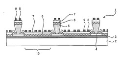
- FIG. 2 is a sectional view taken along line AA in FIG. 1. It is a schematic plan view which shows the other example of the transparent organic EL element of this invention. It is a schematic plan view which shows the other example of the transparent organic EL element of this invention.
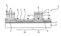
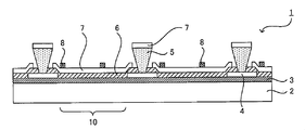
- FIG. 5 is a sectional view taken along line BB in FIG. 4. It is a schematic plan view which shows the other example of the transparent organic EL element of this invention. It is a schematic plan view which shows the other example of the transparent organic EL element of this invention. It is a schematic plan view which shows the other example of the transparent organic EL element of this invention. It is a schematic plan view which shows the other example of the transparent organic EL element of this invention. It is a schematic plan view which shows the other example of the transparent organic EL element of this invention. It is CC sectional view taken on the line of FIG.
- the transparent organic EL device of the present invention includes a transparent substrate, a first transparent electrode layer formed in a stripe shape on the transparent substrate, and the first substrate on which the first transparent electrode layer is formed.
- An insulating partition formed in a stripe shape in a direction orthogonal to the longitudinal direction of the transparent electrode layer, and an organic EL layer formed on the first transparent electrode layer in the light emitting region between the partition and including the light emitting layer
- the angle formed by the longitudinal direction of the partition wall and the extending direction of the thin wires of the first auxiliary electrode group is ⁇ 1 , 0 ° ⁇ 1 ⁇ 90 ° and / or the pitch of the partition walls Remote the pitch of the fine wire of the first auxiliary electrode group is characterized in that narrow.
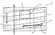
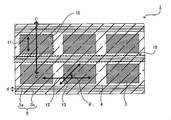
- FIG. 1 is a schematic plan view showing an example of the transparent organic EL device of the present invention
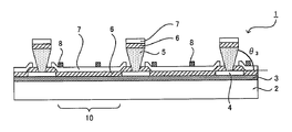
- FIG. 2 is a cross-sectional view taken along line AA in FIG.
- the 1st transparent electrode layer 3 is shown with the dashed-dotted line
- the partition 5 is shown with the dashed-two dotted line.
- a transparent organic EL element 1 illustrated in FIGS. 1 and 2 includes a transparent substrate 2, a first transparent electrode layer 3 formed in a stripe shape on the transparent substrate 2, and a transparent layer on which the first transparent electrode layer 3 is formed.
- An insulating layer 4 is formed on the substrate 2 so that the first transparent electrode layer 3 in the light emitting region 10 is exposed, and a stripe is formed on the insulating layer 4 in a direction perpendicular to the longitudinal direction 11 of the first transparent electrode layer.
- a stripe is formed on the insulating layer 4 in a direction perpendicular to the longitudinal direction 11 of the first transparent electrode layer.
- the second transparent electrode layer 7 divided by the partition walls 5 and the first auxiliary electrode group 8 formed on the second transparent electrode layer 7 and having a plurality of metal thin wires arranged in parallel. ing.
- the first auxiliary electrode group 8 has an angle ⁇ 1 formed between the longitudinal direction 12 of the partition wall and the extending direction 13 of the fine lines of the first auxiliary electrode group, so that 0 ° ⁇ 1
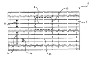
- the fine line pitch p 2 of the first auxiliary electrode group 8 is formed to be narrower than the pitch p 1 of the partition walls 5.
- FIG. 3 is a schematic plan view showing another example of the transparent organic EL element of the present invention. Also in this figure, the 1st transparent electrode layer 3 is shown with the dashed-dotted line, and the partition 5 is shown with the dashed-two dotted line.
- the angle formed by the longitudinal direction of the barrier ribs and the extending direction of the thin wires of the first auxiliary electrode group is 0 ° ⁇ 1 ⁇ 90 ° and / or is greater than the pitch of the barrier ribs. Since the pitch of the thin wires of the one auxiliary electrode group is narrow, the first auxiliary electrode group is surely formed on the second transparent electrode layer formed in the light emitting region between the partition walls, and the second transparent electrode layer even if the alignment is shifted. Resistance can be reduced. Moreover, since the partition is formed, a short circuit does not occur.
- the term “light emitting region” refers to a region contributing to light emission.
- the term “parallel” in the present invention includes a state in which a plurality of straight lines on the same plane are arranged in the same direction so that they do not immediately intersect, in addition to a general parallel case. Specifically, it means a state in which they are arranged in a direction within a range of 0 ° to 10 °.
- partition pitch refers to the distance from the upper bottom end of the partition on the light emitting region side between adjacent partitions to the bottom end of the other upper partition, and “the pitch of the fine lines of the first auxiliary electrode group”. Means the distance from the center of the thin line between adjacent thin lines to the center of the thin line among the plurality of metal thin lines arranged in parallel in the first auxiliary electrode group. These can be measured with an optical microscope, a laser microscope, or a scanning white interferometer.
- the first auxiliary electrode group in the present invention is formed on the second transparent electrode layer, and a plurality of metal thin wires are arranged in parallel. With this first auxiliary electrode group, the resistance of the second transparent electrode layer can be reduced.
- the first auxiliary electrode group in the present invention is an aspect in which 0 ° ⁇ 1 ⁇ 90 °, where ⁇ 1 is an angle formed by the longitudinal direction of the partition walls and the extending direction of the thin wires of the first auxiliary electrode group ( The first mode) and a mode (second mode) in which the pitch of the fine lines of the first auxiliary electrode group is narrower than the pitch of the partition walls can be roughly classified.
- the first auxiliary electrode group is surely formed on the second transparent electrode layer formed in the light emitting region between the partition walls, and the second transparent electrode even if the alignment is misaligned.
- the resistance of the layer can be reduced.
- the partition is formed, a short circuit does not occur.
- the angle ⁇ 1 formed by the longitudinal direction of the partition walls and the extending direction of the thin wires of the first auxiliary electrode group may be 0 ° ⁇ 1 ⁇ 90 °, but ⁇ 1 is small.
- the fine wire of the first auxiliary electrode group can be formed longer between the partition walls, and can function reliably as the auxiliary electrode. Therefore, among them, 0 ° ⁇ 1 ⁇ 45 ° is preferable. It is more preferable that ° ⁇ 1 ⁇ 20 °.
- the first auxiliary electrode group need only have a plurality of metal thin wires formed in parallel so as to form an angle within the above range, and may not be formed in a completely parallel manner. It is preferable that they are formed in parallel.
- the first auxiliary electrode group may be formed on the partition wall as long as it is formed on at least the second transparent electrode layer formed in the light emitting region between the partition walls. Also good.
- the pitch of the thin wires of the first auxiliary electrode group of this aspect is preferably equal to or less than the pitch of the partition walls. This is because the fine lines of the plurality of first auxiliary electrode groups are arranged between the partition walls at the same time, and the function as the auxiliary electrode can be more effectively exhibited. Further, the pitch of the thin lines of the first auxiliary electrode group is appropriately selected according to the angle ⁇ 1 formed by the longitudinal direction of the partition walls and the extending direction of the thin lines of the first auxiliary electrode group, and is constant. It does not have to be constant.
- the first auxiliary electrode group has the second transparent electrode layer formed on the light emitting region between the partition walls by 0 ° ⁇ 1 ⁇ 90 °.
- One auxiliary electrode group is reliably formed.
- the width of the thin wire of the first auxiliary electrode group of this embodiment is preferably in the range of 5 ⁇ m to 300 ⁇ m, and more preferably in the range of 5 ⁇ m to 100 ⁇ m. This is because if the width of the thin line of the first auxiliary electrode group is wider than the above range, the light emitting region is hindered and the aperture ratio of the pixel is lowered. On the other hand, if the width of the thin line of the first auxiliary electrode group is narrower than the above range, the slit of the metal mask used when forming the first auxiliary electrode group also becomes narrow, and the slit is likely to be blocked by the evaporation source. Therefore, it is difficult to form the first auxiliary electrode group, and it is difficult to produce a metal mask itself having a narrow slit for forming such a first auxiliary electrode group. is there.
- the material for the metal thin wire constituting the first auxiliary electrode group of the present embodiment is not particularly limited as long as it is a metal material having a resistance lower than that of the second transparent electrode layer.
- Specific examples include Al, Ag, Au, Cu, Ni, Cr, Mo, Mg, and the like. Among these, Al, Ag, Au, and Mo are preferable.
- a method of forming an electrode using a metal mask can be used. For example, a vacuum evaporation method, a sputtering method, or an ion plating method using a metal mask. And a general vapor deposition method such as a method of applying a metal paste using a metal mask.
- the metal mask it is preferable to use a mask having slits in advance. This is because when the first auxiliary electrode group is formed, bending can be prevented and rigidity can be ensured. Since the metal mask having a slit is thus used, in the transparent organic EL element 1 illustrated in FIG. 1, the first auxiliary electrode group 8 has the disconnection portion 15.
- the transparent organic EL element of the present invention has a partition which will be described later, the second transparent electrode formed in the light emitting region between the partitions without short-circuiting the first auxiliary electrode group by the above forming method. It can be easily formed on the electrode layer.
- the first auxiliary electrode group of this aspect is characterized in that the pitch of the fine lines of the first auxiliary electrode group is narrower than the pitch of the partition walls.
- the partition The first auxiliary electrode group is reliably formed on the second transparent electrode layer formed in the light emitting region therebetween, and the resistance of the second transparent electrode layer can be reduced even if the alignment is shifted.
- the pitch of the fine lines of the first auxiliary electrode group of this embodiment is not particularly limited as long as it is narrower than the pitch of the partition walls. are those selected appropriately according to the angle theta 1 is may be constant or may not be constant. In general, if the pitch of the fine lines of the first auxiliary electrode group is too wide, the first auxiliary electrode group formed on the second transparent electrode layer is reduced, so that the effect of reducing the resistance of the second transparent electrode layer is small. If the pitch of the thin lines of the first auxiliary electrode group is too narrow, the number of first auxiliary electrode groups formed on the second transparent electrode layer increases and the light emitting area is obstructed, so that the aperture ratio of the pixel decreases. End up.
- the other points of the first auxiliary electrode group of this aspect are the same as those of the first aspect, and the description thereof is omitted here.
- the second auxiliary electrode group is further formed on the second transparent electrode layer so as to intersect the first auxiliary electrode group, and a plurality of metal thin wires are arranged in parallel.
- the angle formed by the extending direction of the thin line of the first auxiliary electrode group and the extending direction of the thin line of the second auxiliary electrode group is ⁇ 2 , 0 ° ⁇ 2 ⁇ 90 °, It is preferable that the first auxiliary electrode group and the second auxiliary electrode group are continuously continuous along the longitudinal direction of the partition wall. Since the auxiliary electrode is formed on the second transparent electrode layer formed in the light emitting region between the barrier ribs so as to be connected from end to end, the resistance of the second transparent electrode layer can be further reduced.
- the transparent organic EL device of the present invention further has a second auxiliary electrode group
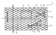
- the first auxiliary electrode group 8 and the second auxiliary electrode group 9 that intersect each other are the second auxiliary electrode group 8 as illustrated in FIGS. 4 and 5.
- the angle formed by the longitudinal direction 12 of the barrier ribs and the extending direction 13 of the fine lines of the first auxiliary electrode group is ⁇ 1
- the extending direction 13 of the fine lines of the first auxiliary electrode group and the first direction are formed on the transparent electrode layer 7.
- the angle formed by the extending direction 14 of the thin wires of the two auxiliary electrode groups is ⁇ 2 , 0 ° ⁇ 1 ⁇ 90 ° and 0 ° ⁇ 2 ⁇ 90 °
- the first auxiliary electrode group 8 and The second auxiliary electrode group 9 is continuous along the longitudinal direction 12 of the partition wall. 6 and 7, even if the second auxiliary electrode group 9 is shifted in the longitudinal direction 12 of the partition wall or in a direction perpendicular to the longitudinal direction 12 of the partition wall, the second auxiliary electrode group 9
- the first auxiliary electrode group 8 and the second auxiliary electrode group 9 are formed on the second transparent electrode layer 7 formed in the light emitting region 10 between the barrier ribs 5 by controlling the pitch of the thin wires 9 and the pitch of the broken portions 15.
- FIG. 4 is schematic plan views showing other examples of the transparent organic EL device of the present invention
- FIG. 5 is a cross-sectional view taken along the line BB of FIG. 4, 6 and 7, the first transparent electrode layer 3 is indicated by a one-dot chain line, and the partition walls 5 are indicated by a two-dot chain line.
- the angle formed by the extending direction of the thin line of the first auxiliary electrode group and the extending direction of the thin line of the second auxiliary electrode group is ⁇ 2 , 0 ° ⁇ 2 ⁇ 90 °. Of these, 0 ° ⁇ 2 ⁇ 45 ° is preferable, and 0 ° ⁇ 2 ⁇ 30 ° is more preferable.
- the second auxiliary electrode group need only have a plurality of metal thin wires formed in parallel so as to form an angle within the above-mentioned range, and may not be formed completely in parallel. It is preferable that they are formed in parallel.
- the second auxiliary electrode group may be symmetric or asymmetric with the first auxiliary electrode group.
- the second auxiliary electrode group may be formed on the partition wall as long as it is formed on at least the second transparent electrode layer formed in the light emitting region between the partition walls. Also good.
- the "pitch of the disconnection part of the second auxiliary electrode group” is a disconnection part between adjacent disconnection parts among a plurality of disconnection parts provided in one metal thin wire constituting the second auxiliary electrode group This is the distance from the center to the center of the disconnected part. These can be measured with an optical microscope, a laser microscope, or a scanning white interferometer.
- the pitch of the fine lines of the second auxiliary electrode group is not particularly limited as long as it can intersect the first auxiliary electrode group, and the extending direction of the fine lines of the first auxiliary electrode group and the second auxiliary electrode group are those selected appropriately depending on the angle theta 2 formed by the extending direction of the fine wire may be constant or may not be constant. Normally, if the pitch of the thin lines of the second auxiliary electrode group is too wide, the number of second auxiliary electrode groups formed on the second transparent electrode layer is reduced, so that the effect of reducing the resistance of the second transparent electrode layer is small. If the pitch of the thin lines of the second auxiliary electrode group is too narrow, the number of second auxiliary electrode groups formed on the second transparent electrode layer increases and the light emitting area is obstructed, so that the aperture ratio of the pixel decreases. End up.
- the width of the thin line of the second auxiliary electrode group is preferably in the range of 5 ⁇ m to 300 ⁇ m, and more preferably in the range of 5 ⁇ m to 100 ⁇ m. This is because if the width of the thin line of the second auxiliary electrode group is wider than the above range, the light emitting region is hindered and the aperture ratio of the pixel is lowered. On the other hand, if the width of the thin line of the second auxiliary electrode group is narrower than the above range, the slit of the metal mask used when forming the second auxiliary electrode group also becomes narrow, and the slit is likely to be blocked by the evaporation source. Therefore, it is difficult to form the second auxiliary electrode group, and it is difficult to produce a metal mask itself having a narrow slit for forming such a second auxiliary electrode group. is there.
- the material and method for forming the second auxiliary electrode group are the same as the material and method for forming the first auxiliary electrode group, and a description thereof will be omitted here. Since the second auxiliary electrode group uses a metal mask with a slit, like the first auxiliary electrode group, in the transparent organic EL element 1 illustrated in FIGS. 4, 6, and 7, The two auxiliary electrode groups 9 also have a disconnection portion 15.
- the material for forming the second auxiliary electrode group may be the same as the material for forming the first auxiliary electrode group, or may be a different material.
- the pitch of the disconnection part of the second auxiliary electrode group is not particularly limited as long as the first auxiliary electrode group and the second auxiliary electrode group can be continuously continuous between the partition walls along the longitudinal direction of the partition walls. Absent.
- the partition walls in the present invention are formed in a stripe shape in a direction orthogonal to the longitudinal direction of the first transparent electrode layer. This partition has insulating properties and is provided to divide the second transparent electrode layer into a plurality of parts.
- the partition wall is also formed in a stripe shape so as to be orthogonal to the longitudinal direction of the stripe-shaped first transparent electrode layer. It is formed.
- the second transparent electrode layer can be divided into a plurality of parts. Therefore, the cross-sectional shape of the partition wall is not particularly limited, and is, for example, rectangular or trapezoidal. (Forward taper shape), reverse taper shape, etc. are mentioned. An overhang shape such as a reverse taper shape is preferable.
- the taper angle ⁇ with respect to the substrate surface may be 0 ° ⁇ ⁇ 90 °, preferably 20 ° ⁇ ⁇ 80 °, more preferably 30 ° ⁇ ⁇ 70 °.
- the taper angle ⁇ refers to a taper angle ⁇ 3 with respect to the surface of the transparent substrate 2 as illustrated in FIG.
- the height of the partition is usually set such that the height from the base surface of the partition to the surface of the partition is higher than the height from the transparent substrate surface to the second transparent electrode layer surface at the center of the light emitting region. .
- the width of the partition wall is not particularly limited, but is preferably 100 ⁇ m or less. This is because if the partition wall is too wide, the light emitting region becomes relatively narrow.
- the pitch of the partition walls is not particularly limited, and is appropriately selected depending on the pixel size of the target transparent organic EL element.
- Each of the partition walls may be composed of a plurality of small partition walls provided in parallel at a predetermined interval.
- the organic layer constituting the organic EL layer is formed by a printing method, it is preferable to provide a plurality of small partition walls as described above. This is because the second transparent electrode layer can be divided even when ink adheres to the side surface of the partition wall and the organic layer becomes thicker around the partition wall.
- each of the partition walls 5 is composed of two small partition walls 5a and a small partition wall 5b provided in parallel at a predetermined interval d.
- FIG. 8 is a schematic plan view showing another example of the transparent organic EL element of the present invention.
- FIG. 9 is a cross-sectional view taken along the line CC of FIG. 8. In FIG. 8, the organic EL layer and the second transparent EL element are shown. The electrode layer is omitted.
- the interval between the small barrier ribs may be an interval that can divide the second transparent electrode layer. Specifically, it is preferably in the range of 1 ⁇ m to 60 ⁇ m, and in the range of 1 ⁇ m to 30 ⁇ m. More preferably, it is more preferably in the range of 1 ⁇ m to 10 ⁇ m.
- the interval between the small partition walls is wider than the above range, for example, when the organic layer constituting the organic EL layer is formed by a printing method, the organic layer forming coating liquid easily enters between the small partition walls, and the second transparent This is because it may be difficult to divide the electrode layer.
- the organic layer may be continuously formed between the small partition walls. Because it does.
- the “interval between the small partition walls” refers to the distance from the end of the upper bottom surface to the end of the upper bottom surface of the plurality of small partition walls constituting the partition wall, which is an optical microscope or laser microscope. It can be measured by a scanning white interferometer.
- the width of the divided region defined by the partition walls is preferably 300 ⁇ m or less. This is because if the width of the divided region is wider than the above range, the light emitting region becomes relatively narrow.
- region demarcated by a partition means the parting area
- partition wall forming material examples include photosensitive polyimide resins, acrylic resins, novolac resins, styrene resins, phenol resins, melamine resins, and other photo-curing resins, thermosetting resins, and inorganic materials. Can be mentioned.
- a general method such as a photolithography method or a printing method can be used.
- the second transparent electrode layer in the present invention is formed on the organic EL layer, and is parted by the said partition.
- the second transparent electrode layer may be an anode or a cathode, but is usually formed as a cathode.
- the transparent organic EL device of the present invention light can be extracted from both sides, and the second transparent electrode layer needs to be transparent or translucent.
- the material of the second transparent electrode layer is not particularly limited as long as it is a conductive material capable of forming a transparent electrode.
- a conductive material capable of forming a transparent electrode.
- ITO indium tin oxide
- IZO indium zinc oxide
- AZO aluminum zinc oxide
- metals such as Au and Ni
- conductive polymers such as polyaniline, polyacetylene, polyalkylthiophene derivatives, polysilane derivatives, etc. Can be mentioned.
- a general electrode forming method can be used as a method for forming the second transparent electrode layer.
- a PVD method such as a vacuum deposition method, a sputtering method, an ion plating method, a CVD method, a conductive paste, or the like.
- coating is mentioned.
- a vacuum deposition method and a method of applying a conductive paste are preferable.
- the vacuum evaporation method is a method that causes little damage to the organic EL layer in a dry process and is suitable for stacking.
- the method of applying the conductive paste is a wet process, and the wet process is more suitable for dealing with a larger area than the dry process.
- a conductive paste containing a solvent that does not affect the organic EL layer can be used. That is, a wet process can be applied by devising the organic EL layer so as not to be affected by the solvent resistance of the organic EL layer.
- the organic EL layer in the present invention is formed on the first transparent electrode layer in the light emitting region between the partition walls, and includes at least a light emitting layer.
- the organic EL layer may be formed on at least the first transparent electrode layer in the light emitting region between the partition walls.
- the organic EL layer 6 may be formed on the partition wall 5, and as shown in FIG. 10, the organic EL layer 6 may not be formed on the partition wall 5. .
- the organic EL layer 6 may be formed on the entire surface of the partition wall 5. You may form in a part on a partition.
- FIG. 10 is a schematic cross-sectional view showing another example of the transparent organic EL element of the present invention, and reference numerals that are not described may be the same as those in FIG. .
- the organic EL layer used in the present invention has one or more organic layers including at least a light emitting layer. That is, the organic EL layer is a layer including at least a light emitting layer, and the layer configuration is a layer having one or more organic layers.
- the organic EL layer is formed by a wet process by coating, it is often difficult to stack a large number of layers in relation to a solvent, so that it is often composed of one or two organic layers.
- it is possible to further increase the number of layers by devising organic materials or combining vacuum deposition methods.
- Examples of the organic layer constituting the organic EL layer other than the light emitting layer include a hole injection layer, an electron injection layer, a hole transport layer, and an electron transport layer.
- the hole transport layer may be integrated with the hole injection layer by imparting a hole transport function to the hole injection layer.
- the electron transport layer may be integrated with the electron injection layer by adding an electron transport function to the electron injection layer.
- an organic layer which comprises an organic EL layer the layer etc. for preventing the penetration of a hole or an electron like a carrier block layer, and improving recombination efficiency can be mentioned.
- the organic EL layer in the present invention will be described for each configuration.
- Light emitting layer As a material used for the light emitting layer in this invention, light emitting materials, such as a pigment-type material, a metal complex type material, a polymeric material, can be mentioned, for example.
- dye materials include cyclopentadiene derivatives, tetraphenylbutadiene derivatives, triphenylamine derivatives, oxadiazole derivatives, pyrazoloquinoline derivatives, distyrylbenzene derivatives, distyrylarylene derivatives, silole derivatives, thiophene ring compounds, pyridine ring compounds.
- the metal complex material examples include an aluminum quinolinol complex, a benzoquinolinol beryllium complex, a benzoxazole zinc complex, a benzothiazole zinc complex, an azomethylzinc complex, a porphyrin zinc complex, and a eurobium complex.
- a metal complex having a rare earth metal such as Tb, Eu, or Dy and having a ligand such as oxadiazole, thiadiazole, phenylpyridine, phenylbenzimidazole, or quinoline structure can be given.
- examples of the polymer material include polyparaphenylene vinylene derivatives, polythiophene derivatives, polyparaphenylene derivatives, polysilane derivatives, polyacetylene derivatives, polyvinyl carbazole, polyfluorene derivatives, polyquinoxaline derivatives, and copolymers thereof. Can be mentioned.
- a doping agent may be added for the purpose of improving the light emission efficiency and changing the light emission wavelength.
- doping agents include perylene derivatives, coumarin derivatives, rubrene derivatives, quinacridone derivatives, squalium derivatives, porphyrin derivatives, styryl dyes, tetracene derivatives, pyrazoline derivatives, decacyclene, phenoxazone, quinoxaline derivatives, carbazole derivatives, fluorene derivatives. Can be mentioned.
- the thickness of the light-emitting layer is not particularly limited as long as it can provide a function of emitting light by providing a recombination field between electrons and holes, and is, for example, about 1 nm to 500 nm. can do.
- the light emitting layer is divided by the barrier ribs and formed into a pattern.
- the light emitting layer is preferably formed in a pattern so as to have light emitting portions of a plurality of colors such as red, green, and blue.
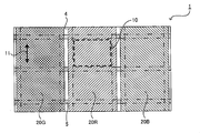
- the red light emitting portion 20R, the green light emitting portion 20G, and the blue light emitting portion 20B are parallel and striped with respect to the longitudinal direction 11 of the striped first transparent electrode layer.
- FIG. 11 the red light emitting portion 20R, the green light emitting portion 20G, and the blue light emitting portion 20B are parallel and striped with respect to the longitudinal direction 11 of the striped first transparent electrode layer.
- the red light emitting portion 20R, the green light emitting portion 20G, and the blue light emitting portion 20B are arranged with respect to the longitudinal direction 11 of the striped first transparent electrode layer. They may be arranged vertically and in stripes.
- 11 and 12 are schematic plan views showing other examples of the transparent organic EL device of the present invention.
- the first transparent electrode layer 3 is indicated by a one-dot chain line
- the partition wall 5 is indicated by a two-dot chain line.
- the second transparent electrode layer 7 and the first auxiliary electrode group 8 are omitted.
- the formation method of the light emitting layer is not particularly limited as long as it is a method capable of high-definition patterning.
- vapor deposition method printing method, ink jet method, transfer method, dip coating method, roll coating method, blade coating method, spin coating method, bar coating method, wire bar coating method, casting method, LB method, etc.
- vapor deposition method printing method, ink jet method, transfer method, dip coating method, roll coating method, blade coating method, spin coating method, bar coating method, wire bar coating method, casting method, LB method, etc.
- the hole transport layer may be integrated with the hole injection layer by imparting a hole transport function to the hole injection layer. That is, the hole injection layer may have only a hole injection function, or may have both a hole injection function and a hole transport function.
- the material used for the hole injection layer is not particularly limited as long as it can stabilize the injection of holes into the light emitting layer, and the compounds exemplified as the light emitting material for the light emitting layer.
- phenylamine materials, starburst amine materials, phthalocyanine materials, vanadium oxide, molybdenum oxide, ruthenium oxide, aluminum oxide, titanium oxide and other oxides, amorphous carbon, polyaniline, polythiophene, polyphenylene vinylene derivatives, etc. Can be used.
- ⁇ -NPD bis (N- (1-naphthyl) -N-phenyl) benzidine
- MTDATA 4,4,4-tris (3-methylphenylphenylamino) triphenylamine
- PEDOT-PSS poly-3 4,4 ethylenedioxythiophene-polystyrene sulfonic acid
- PVCz polyvinyl carbazole
- the thickness of the hole injection layer is not particularly limited as long as the hole injection function and the hole transport function are sufficiently exerted. Specifically, the thickness is in the range of 0.5 nm to 1000 nm, particularly 10 nm. It is preferably in the range of ⁇ 500 nm.
- the method for forming the hole injection layer is the same as the method for forming the light emitting layer.
- the electron transport layer may be integrated with the electron injection layer by imparting an electron transport function to the electron injection layer. That is, the electron injection layer may have only an electron injection function, or may have both an electron injection function and an electron transport function.
- the material used for the electron injection layer is not particularly limited as long as it can stabilize the injection of electrons into the light emitting layer.
- Aluminum lithium alloy, lithium fluoride, strontium, magnesium oxide, magnesium fluoride, strontium fluoride, calcium fluoride, barium fluoride, aluminum oxide, strontium oxide, calcium, polymethyl methacrylate, sodium polystyrene sulfonate, lithium, cesium Alkali metals such as cesium fluoride, alkali metal halides, alkali metal organic complexes, and the like can be used.
- a metal doped layer in which an alkali metal or alkaline earth metal is doped on an electron transporting organic material, and this can be used as an electron injection layer.
- the electron-transporting organic material include bathocuproine, bathophenanthroline, and phenanthroline derivatives.
- the metal to be doped include Li, Cs, Ba, and Sr.
- the thickness of the electron injection layer is not particularly limited as long as the electron injection function and the electron transport function are sufficiently exhibited. Moreover, as a formation method of an electron injection layer, a vacuum evaporation method is mentioned, for example.
- Electron transport layer The material used for the electron transport layer is not particularly limited as long as it is a material capable of transporting electrons injected from the cathode into the light emitting layer.
- bathocuproine Examples include bathophenanthroline, phenanthroline derivatives, triazole derivatives, oxadiazole derivatives, and derivatives of tris (8-quinolinolato) aluminum complex (Alq 3 ).
- the thickness of the electron transport layer is not particularly limited as long as the electron transport function is sufficiently exerted.
- the method for forming the electron transport layer is the same as the method for forming the light emitting layer.
- the 1st transparent electrode layer in this invention is formed in a stripe form on a transparent substrate.
- the first transparent electrode layer may be an anode or a cathode, but is usually formed as an anode.
- the transparent organic EL element of the present invention light can be extracted from both sides, and the first transparent electrode layer needs to be transparent or translucent.
- the material of the first transparent electrode layer is not particularly limited as long as it is a conductive material capable of forming a transparent electrode.
- a conductive material capable of forming a transparent electrode.
- ITO indium tin oxide
- IZO indium zinc oxide
- AZO aluminum zinc oxide
- metals such as Au and Ni
- conductive polymers such as polyaniline, polyacetylene, polyalkylthiophene derivatives, polysilane derivatives, etc. Can be mentioned.
- a film formation method for the first transparent electrode layer a general electrode film formation method can be used.
- a PVD method such as a vacuum evaporation method, a sputtering method, an ion plating method, a CVD method, or the like can be given.
- the patterning method of the first transparent electrode layer is not particularly limited as long as it can be accurately formed into a desired pattern, and specific examples thereof include a photolithography method. .
- the transparent substrate in the present invention is not particularly limited as long as it supports the above-described partition walls, the first transparent electrode layer, and the like and has a predetermined strength.
- the first transparent electrode layer may also serve as the transparent substrate.
- the first transparent electrode layer is formed on the transparent substrate having the predetermined strength.
- One transparent electrode layer is formed.
- Examples of the material for forming such a transparent substrate include glass plates such as soda lime glass, alkali glass, lead alkali glass, borosilicate glass, aluminosilicate glass, and silica glass, or resin substrates that can be formed into a film. Can be used.
- the resin used for the resin substrate is preferably a polymer material having relatively high solvent resistance and heat resistance.
- fluorine resin polyethylene, polypropylene, polyvinyl chloride, polyvinyl fluoride, polystyrene, ABS resin, polyamide, polyacetal, polyester, polycarbonate, modified polyphenylene ether, polysulfone, polyarylate, polyetherimide, polyether mon Phon, Polyamideimide, Polyimide, Polyphenylene sulfide, Liquid crystalline polyester, Polyethylene terephthalate, Polybutylene terephthalate, Polyethylene naphthalate, Polymicroxylene dimethylene terephthalate, Polyoxymethylene, Polyethersulfone, Polyetheretherketone, Polyacrylate, Acrylonitrile -Styrene resin, phenol resin, urea resin, melamine resin, unsaturated polyester resin, Epoxy resins, polyurethane, silicone resin, amorphous polyolefins, and the like.
- any polymer material that satisfies a predetermined condition can be used, and two or more types of copolymers can be used.
- the transparent substrate which has gas barrier property which interrupts
- an insulating layer is preferably formed between the first transparent electrode layer and the partition. It is because it can prevent that a 1st transparent electrode layer and a 2nd transparent electrode layer contact and short-circuit.
- This insulating layer is preferably formed so as to cover the end of the first transparent electrode layer. Since the thickness of the organic EL layer is reduced at the end of the first transparent electrode layer, it is possible to make short-circuiting difficult by forming an insulating layer. In addition, it is possible to prevent the adjacent light emitting regions from being electrically connected.
- the portion where the insulating layer is formed can be a region that does not contribute to light emission.
- the insulating layer may be formed so that the first transparent electrode layer in the light emitting region is exposed.
- the size of the light emitting region is not particularly limited, and is appropriately set according to the use of the transparent organic EL element.
- Examples of the material for forming the insulating layer include photo-curing resins such as photosensitive polyimide resins and acrylic resins, thermosetting resins, and inorganic materials.
- a general method such as a photolithography method or a printing method can be used.
- the transparent organic EL device of the present invention is formed in a stripe shape so that the first transparent electrode layer and the second transparent electrode layer cross each other, and is suitably used as a passive transparent organic EL device. .
- the method for producing a transparent organic EL device of the present invention includes a transparent substrate, a first transparent electrode layer formed in a stripe shape on the transparent substrate, and the transparent substrate on which the first transparent electrode layer is formed.
- Insulating barrier ribs formed in stripes in a direction orthogonal to the longitudinal direction of the first transparent electrode layer, and formed on the first transparent electrode layer in the light emitting region between the barrier ribs and including a light emitting layer
- An organic EL layer a second transparent electrode layer formed on the organic EL layer and separated by the partition, a plurality of metal thin wires formed in parallel on the second transparent electrode layer A first auxiliary electrode group, and a second auxiliary electrode formed on the second transparent electrode layer so as to intersect the first auxiliary electrode group, and a plurality of metal thin wires arranged in parallel.
- a method for producing a transparent organic EL device having an electrode group When the angle formed by the extending direction of the longitudinal direction and the first auxiliary electrode group thin line of the bulkhead and the theta 1, form a 0 ° ⁇ 1 ⁇ 90 ° and so as to the first auxiliary electrode group a first auxiliary electrode group forming step of, when the angle formed by the extending direction of the first auxiliary electrode group of the extending direction and the second auxiliary electrode group of fine wire fine line and theta 2, 0 ° ⁇ and a second auxiliary electrode group forming step of forming the second auxiliary electrode group so that ⁇ 2 ⁇ 90 °.
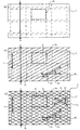
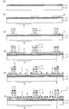
- FIG. 15 are process diagrams showing an example of the method for producing the transparent organic EL element of the present invention.
- 13 (a) to 13 (c) and 14 (a) to 14 (c) are schematic plan views, and FIG. 15 (a) is a sectional view taken along the line DD of FIG. 13 (a).
- 15 (b) is a sectional view taken along line EE in FIG. 13 (b)
- FIG. 15 (c) is a sectional view taken along line FF in FIG. 13 (c)
- FIG. 15 (d) is a sectional view taken along line G in FIG.
- FIG. 15E is a cross-sectional view taken along the line H-H in FIG.
- FIG. 14B, and FIG. 15F is a cross-sectional view taken along the line II in FIG. 14C.
- the first transparent electrode layer 3 is indicated by a one-dot chain line
- FIGS. 14 (a) to 14 (c) is indicated by a two-dot chain line.
- a striped first transparent electrode layer 3 is formed on the transparent substrate 2 (FIGS. 13A and 15A).
- the insulating layer 4 is formed on the transparent substrate 2 on which the first transparent electrode layer 3 is formed so that the first transparent electrode layer 3 in the light emitting region 10 is exposed (FIG. 13B and FIG. 15).
- the insulating partition walls 5 are formed in stripes extending in the direction perpendicular to the longitudinal direction 11 of the first transparent electrode layer on the insulating layer 4 (FIGS. 13C and 15C). .
- an organic EL layer 6 is formed on the entire surface of the transparent substrate 2 on which the partition walls 5 are formed, and a second transparent electrode layer 7 is further formed on the organic EL layer 6 (FIG. 14A and FIG. 15 (d)).
- the first auxiliary electrode group 8 is formed by vapor deposition using a metal mask (FIG. 14B and FIG. 15E, first auxiliary electrode group forming step).
- the second auxiliary electrode group 9 is formed by vapor deposition using a metal mask (FIG. 14C and FIG. 15F, second auxiliary electrode group forming step).
- the transparent organic EL element 1 in which the first auxiliary electrode group 8 and the second auxiliary electrode group 9 intersecting each other is formed on the second transparent electrode layer 7 formed in the light emitting region 10 between the partition walls 5 is obtained. It is done.
- the auxiliary electrode is formed by forming the first auxiliary electrode group and the second auxiliary electrode group in a predetermined angular direction so as to cross each other, the first auxiliary electrode group is formed in the light emitting region between the barrier ribs.
- the two transparent electrode layers it is possible to reliably and easily form the auxiliary electrode continuously without a break, and to reduce the resistance of the second transparent electrode layer.
- the contact between the first auxiliary electrode group and the second auxiliary electrode group can be secured, and a short circuit is not caused by the partition wall. There is no need to perform this, and the manufacturing tact can be shortened.
- the first auxiliary electrode group forming step in the present invention will be described.
- the angle formed by the longitudinal direction of the partition walls and the extending direction of the thin lines of the first auxiliary electrode group is ⁇ 1 , 0 ° ⁇ 1 ⁇ 90 °. In this way, the first auxiliary electrode group is formed.
- first auxiliary electrode group and the method for forming the first auxiliary electrode group are described in the above section “A. Transparent organic EL element”, the description thereof is omitted here.
- the second auxiliary electrode group formation step in the present invention when the angle formed by the extending direction and the extending direction of the second auxiliary electrode group of the thin line of the thin line of the first auxiliary electrode group was theta 2, 0 ° ⁇ In this step, the second auxiliary electrode group is formed so that ⁇ 2 ⁇ 90 °.
- the method for producing a transparent organic EL device of the present invention includes a first transparent electrode layer forming step, an insulating layer, in addition to the first auxiliary electrode group forming step and the second auxiliary electrode group forming step, which are essential steps.
- You may have a formation process, a partition formation process, an organic EL layer formation process, a 2nd transparent electrode layer formation process, etc.
- the present invention is not limited to the above embodiment.
- the above-described embodiment is an exemplification, and the present invention has the same configuration as the technical idea described in the claims of the present invention. It is included in the technical scope of the invention.
- Example 10 (Formation of first transparent electrode layer) First, an indium tin oxide (ITO) electrode film having a thickness of 200 nm is formed on a glass substrate (thickness 0.7 mm) by an ion plating method, a photosensitive resist is applied on the ITO electrode film, and mask exposure is performed. Then, development and etching of the ITO electrode film were performed, the resist was peeled off, and 100 stripe-shaped first transparent electrode layers having a width of 0.8 mm and a length of 30 mm were formed at a pitch of 1 mm.
- ITO indium tin oxide
- the glass substrate on which the first transparent electrode layer is formed is subjected to a cleaning process and an ultraviolet plasma cleaning, and then a positive photosensitive resist mainly composed of a polyimide precursor is applied by a spin coating method. Patterning was performed by a lithography process to form an insulating layer (thickness: 1.5 ⁇ m) such that light emitting regions (openings) of 0.7 mm ⁇ 0.7 mm existed at a pitch of 1 mm on each first transparent electrode layer.
- the substrate on which the resist film is formed is developed with an alkali developer to form a resist pattern, and cured by heat treatment (post-bake) so as to be orthogonal to the first transparent electrode layer on the insulating layer.
- 11 partition walls having a stripe shape with a width of 30 ⁇ m and a length of 200 mm and a reverse tapered shape were formed at a pitch of 1 mm.
- a hole injection layer was formed by gravure offset printing on the first transparent electrode layer on which the partition walls were formed. That is, the cell shape and ink concentration of the gravure plate are adjusted so that a desired film thickness is obtained, the gravure plate and blanket are mounted on a flat table offset printing machine, and the hole injection layer ink (polyethylenedioxy) is attached to the gravure plate. Thiophene-polystyrene sulfonate (PEDOT-PSS)) was supplied, and the ink for the hole injection layer was filled in the cell.
- PEDOT-PSS Thiophene-polystyrene sulfonate
- the hole injection layer ink is transferred by accepting the ink for the hole injection layer from the gravure plate to the blanket, and then transferring the ink for the hole injection layer from the blanket onto the substrate on which the partition wall is formed.
- a layer was formed.
- a light emitting layer was formed by a gravure offset printing method using a light emitting layer ink (polyfluorene derivative-based green light emitting material).
- an electron injection layer was formed on the light emitting layer by depositing calcium with a thickness of 20 nm by a vacuum deposition method using a metal mask.
- an indium zinc oxide (IZO) electrode film (thickness: 150 nm) was formed on the electron injection layer by a sputtering method to form a second transparent electrode layer.
- the introduction amount of oxygen gas 0.04 when the introduction amount of oxygen gas is 0.2 cc and the introduction amount of argon gas is 5.0 cc, the introduction amount of oxygen gas or oxygen gas
- the oxygen ratio (oxygen / argon ratio) was changed from 0.00 to 0.20.
- the pressure was 0.2 Pa, the output was DC 900 W, and the film formation rate was 12.0 ⁇ / s.
- the luminance difference between the pixels at both ends in the longitudinal direction of the second transparent electrode layer was within 10%.
- the luminance difference between the pixels at both ends in the longitudinal direction of the second transparent electrode layer was 50%, and luminance unevenness was observed. This is considered because the resistance of the second transparent electrode layer could be reduced by forming the auxiliary electrode in the example.
Landscapes
- Physics & Mathematics (AREA)
- Optics & Photonics (AREA)
- Electroluminescent Light Sources (AREA)
Abstract
本発明は、簡便な工程で第2電極層上に確実に補助電極を形成することができ、アライメントがずれても短絡を起こすことなく第2電極層の抵抗を低減することが可能な透明有機EL素子を提供することを主目的とする。 本発明においては、透明基板と、上記透明基板上にストライプ状に形成された第1透明電極層と、上記第1透明電極層が形成された上記透明基板上に、上記第1透明電極層の長手方向と直交する方向にストライプ状に形成された絶縁性の隔壁と、上記隔壁間の発光領域内の上記第1透明電極層上に形成され、かつ発光層を含む有機EL層と、上記有機EL層上に形成され、かつ上記隔壁により分断されている第2透明電極層と、上記第2透明電極層上に形成され、かつ金属製の細線が複数本平行に配置されてなる第1補助電極群とを有する透明有機EL素子であって、上記隔壁の長手方向および上記第1補助電極群の細線の延在方向により形成される角度をθ1としたとき、0°<θ1<90°であること、および/または、上記隔壁のピッチよりも上記第1補助電極群の細線のピッチが狭いことを特徴とする透明有機EL素子を提供することにより、上記課題を解決する。
Description
本発明は、隔壁を有し、第2電極層上に抵抗を低下させるための補助電極が形成されているパッシブ型の有機エレクトロルミネッセンス素子に関するものである。
有機発光層を一対の電極の間に挟み、両電極間に電圧をかけて発光させる有機エレクトロルミネッセンス(以下、エレクトロルミネッセンスをELと略す場合がある。)素子は、自己発色により視認性が高いこと、液晶素子と異なり全固体素子であるため耐衝撃性に優れていること、応答速度が速いこと、温度変化による影響が少ないこと、および、視野角が大きいことなどの利点を有しており、表示装置における発光素子としての利用が注目されている。
このような有機EL素子において、有機発光層の両側にある第1電極および第2電極を透明電極とした透明パネルを作製する場合、第2電極の抵抗が高いために、表示ムラが発生するという問題があった。
そこで、第2電極の抵抗を下げるために、第2電極用の補助電極をガラス基板上に形成させて、スルーホールで接続させる方法が提案されているが(特許文献1参照)、この方法では、工程が増えて複雑になる問題がある。一方、補助電極を直接第2電極上に形成する方法が提案されている(特許文献2参照)。しかしながら、この方法においては、マトリクス状配列に従って並ぶ発光素子の間に補助電極を形成するため、アライメントの調整が難しいといった問題がある。
本発明は、上記問題点に鑑みてなされたものであり、簡便な工程で第2電極層上に確実に補助電極を形成することができ、アライメントがずれても短絡を起こすことなく、第2電極層の抵抗を低減することが可能な透明有機EL素子およびその製造方法を提供することを主目的とする。
上記目的を達成するために、本発明は、透明基板と、上記透明基板上にストライプ状に形成された第1透明電極層と、上記第1透明電極層が形成された上記透明基板上に、上記第1透明電極層の長手方向と直交する方向にストライプ状に形成された絶縁性の隔壁と、上記隔壁間の発光領域内の上記第1透明電極層上に形成され、かつ発光層を含む有機EL層と、上記有機EL層上に形成され、かつ上記隔壁により分断されている第2透明電極層と、上記第2透明電極層上に形成され、かつ金属製の細線が複数本平行に配置されてなる第1補助電極群とを有する透明有機EL素子であって、上記隔壁の長手方向および上記第1補助電極群の細線の延在方向により形成される角度をθ1としたとき、0°<θ1<90°であること、および/または、上記隔壁のピッチよりも上記第1補助電極群の細線のピッチが狭いことを特徴とする透明有機EL素子を提供する。
本発明によれば、隔壁の長手方向および第1補助電極群の細線の延在方向により形成される角度が0°<θ1<90°であること、および/または、隔壁のピッチよりも第1補助電極群の細線のピッチが狭いことにより、隔壁間の発光領域に形成された第2透明電極層上に第1補助電極群が確実に形成され、アライメントがずれても第2透明電極層の抵抗を低下させることができる。また、隔壁が形成されているため、短絡を起こすことがない。
上記発明においては、さらに上記第2透明電極層上に上記第1補助電極群と交差するように形成され、かつ金属製の細線が複数本平行に配置されてなる第2補助電極群を有し、上記第1補助電極群の細線の延在方向および上記第2補助電極群の細線の延在方向により形成される角度をθ2としたとき、0°<θ2≦90°であり、上記第1補助電極群および上記第2補助電極群が、上記隔壁の長手方向に沿って切れ目なく連続していることが好ましい。隔壁間の発光領域に形成された第2透明電極層上に、補助電極が端から端までつながるように形成されていることで、第2透明電極層の抵抗をより低下させることができるからである。また、補助電極のアライメントがずれても、第1補助電極群と第2補助電極群との接点を確保することができ、かつ、隔壁により短絡を起こすことがないため、補助電極のアライメントを調整する必要がない。
また、本発明は、透明基板と、上記透明基板上にストライプ状に形成された第1透明電極層と、上記第1透明電極層が形成された上記透明基板上に、上記第1透明電極層の長手方向と直交する方向にストライプ状に形成された絶縁性の隔壁と、上記隔壁間の発光領域内の上記第1透明電極層上に形成され、かつ発光層を含む有機EL層と、上記有機EL層上に形成され、かつ上記隔壁により分断されている第2透明電極層と、上記第2透明電極層上に形成され、かつ金属製の細線が複数本平行に配置されてなる第1補助電極群と、上記第2透明電極層上に上記第1補助電極群と交差するように形成され、かつ金属製の細線が複数本平行に配置されてなる第2補助電極群とを有する透明有機EL素子の製造方法であって、上記隔壁の長手方向および上記第1補助電極群の細線の延在方向により形成される角度をθ1としたとき、0°<θ1<90°となるように上記第1補助電極群を形成する第1補助電極群形成工程と、上記第1補助電極群の細線の延在方向および上記第2補助電極群の細線の延在方向により形成される角度をθ2としたとき、0°<θ2≦90°となるように上記第2補助電極群を形成する第2補助電極群形成工程とを有することを特徴とする透明有機EL素子の製造方法を提供する。
本発明によれば、互いに交差するように第1補助電極群および第2補助電極群をそれぞれ所定の角度方向に形成することにより補助電極を形成するため、隔壁間の発光領域に形成された第2透明電極層上に、確実かつ容易に補助電極を切れ目なく連続して形成することができ、第2透明電極層の抵抗を下げることができる。また、補助電極のアライメントがずれても、第1補助電極群と第2補助電極群との接点を確保することができ、かつ、隔壁により短絡を起こすことがないため、補助電極のアライメント調整を行う必要がなく、製造タクトの短縮化を図ることができる。
本発明においては、簡便な工程で第2電極層上に確実に補助電極を形成することができ、アライメントがずれても短絡を起こすことなく、第2電極層の抵抗を下げることができるという効果を奏する。
以下、本発明の透明有機EL素子および透明有機EL素子の製造方法について詳細に説明する。
A.透明有機EL素子
まず、本発明の透明有機EL素子について説明する。本発明の透明有機EL素子は、透明基板と、上記透明基板上にストライプ状に形成された第1透明電極層と、上記第1透明電極層が形成された上記透明基板上に、上記第1透明電極層の長手方向と直交する方向にストライプ状に形成された絶縁性の隔壁と、上記隔壁間の発光領域内の上記第1透明電極層上に形成され、かつ発光層を含む有機EL層と、上記有機EL層上に形成され、かつ上記隔壁により分断されている第2透明電極層と、上記第2透明電極層上に形成され、かつ金属製の細線が複数本平行に配置されてなる第1補助電極群とを有するものであって、上記隔壁の長手方向および上記第1補助電極群の細線の延在方向により形成される角度をθ1としたとき、0°<θ1<90°であること、および/または、上記隔壁のピッチよりも上記第1補助電極群の細線のピッチが狭いことを特徴とするものである。
まず、本発明の透明有機EL素子について説明する。本発明の透明有機EL素子は、透明基板と、上記透明基板上にストライプ状に形成された第1透明電極層と、上記第1透明電極層が形成された上記透明基板上に、上記第1透明電極層の長手方向と直交する方向にストライプ状に形成された絶縁性の隔壁と、上記隔壁間の発光領域内の上記第1透明電極層上に形成され、かつ発光層を含む有機EL層と、上記有機EL層上に形成され、かつ上記隔壁により分断されている第2透明電極層と、上記第2透明電極層上に形成され、かつ金属製の細線が複数本平行に配置されてなる第1補助電極群とを有するものであって、上記隔壁の長手方向および上記第1補助電極群の細線の延在方向により形成される角度をθ1としたとき、0°<θ1<90°であること、および/または、上記隔壁のピッチよりも上記第1補助電極群の細線のピッチが狭いことを特徴とするものである。
本発明の透明有機EL素子について、図面を参照しながら説明する。図1は、本発明の透明有機EL素子の一例を示す概略平面図、図2は図1のA-A線断面図である。図1において、第1透明電極層3を一点鎖線で、隔壁5を二点鎖線で示している。
図1および図2に例示する透明有機EL素子1は、透明基板2と、透明基板2上にストライプ状に形成された第1透明電極層3と、第1透明電極層3が形成された透明基板2上に、発光領域10内の第1透明電極層3が露出するように形成された絶縁層4と、絶縁層4上に、第1透明電極層の長手方向11と直交する方向にストライプ状に形成された絶縁性の隔壁5と、隔壁5間の発光領域10内の第1透明電極層3上に形成され、発光層を含む有機EL層6と、有機EL層6上に形成され、隔壁5により分断されている第2透明電極層7と、第2透明電極層7上に形成され、金属製の細線が複数本平行に配置されてなる第1補助電極群8とを有している。
図1および図2に例示する透明有機EL素子1は、透明基板2と、透明基板2上にストライプ状に形成された第1透明電極層3と、第1透明電極層3が形成された透明基板2上に、発光領域10内の第1透明電極層3が露出するように形成された絶縁層4と、絶縁層4上に、第1透明電極層の長手方向11と直交する方向にストライプ状に形成された絶縁性の隔壁5と、隔壁5間の発光領域10内の第1透明電極層3上に形成され、発光層を含む有機EL層6と、有機EL層6上に形成され、隔壁5により分断されている第2透明電極層7と、第2透明電極層7上に形成され、金属製の細線が複数本平行に配置されてなる第1補助電極群8とを有している。
この第1補助電極群8は、図1に例示するように、隔壁の長手方向12と第1補助電極群の細線の延在方向13とで形成される角度θ1が、0°<θ1<90°となるように、または、図3に例示するように、隔壁5のピッチp1よりも第1補助電極群8の細線のピッチp2が狭くなるように形成されている。なお、図3は本発明の透明有機EL素子の他の例を示す概略平面図である。この図においても、第1透明電極層3を一点鎖線で、隔壁5を二点鎖線で示している。
本発明によれば、隔壁の長手方向および第1補助電極群の細線の延在方向により形成される角度が0°<θ1<90°であること、および/または、隔壁のピッチよりも第1補助電極群の細線のピッチが狭いことにより、隔壁間の発光領域に形成された第2透明電極層上に第1補助電極群が確実に形成され、アライメントがずれても第2透明電極層の抵抗を低下させることができる。また、隔壁が形成されているため、短絡を起こすことがない。
なお、「発光領域」とは、発光に寄与する領域をいう。また、本発明における「平行」とは、一般的な平行の場合の他、同一平面上の複数の直線がすぐには交差しない同一方向に並んでいる状態を含むものとする。具体的には、0°~10°の範囲内の方向に並んでいる状態をいう。
また、「隔壁のピッチ」とは、隣接する隔壁間の発光領域側の隔壁上底面端部から他の隔壁上底面端部までの距離をいい、「第1補助電極群の細線のピッチ」とは、第1補助電極群において複数本平行に配置された金属製の細線のうち、隣接する細線間の細線中央から細線中央までの距離をいう。これらは、光学顕微鏡、レーザ顕微鏡、走査型白色干渉計により測定することができる。
以下、本発明の透明有機EL素子における各構成について説明する。
1.第1補助電極群
本発明における第1補助電極群は、第2透明電極層上に形成され、かつ金属製の細線が複数本平行に配置されてなるものである。この第1補助電極群により、第2透明電極層の抵抗を低減することができる。本発明における第1補助電極群は、隔壁の長手方向および第1補助電極群の細線の延在方向により形成される角度をθ1としたとき、0°<θ1<90°である態様(第1態様)、および、隔壁のピッチよりも第1補助電極群の細線のピッチが狭い態様(第2態様)に大別することができる。以下、態様ごとに分けて説明する。
本発明における第1補助電極群は、第2透明電極層上に形成され、かつ金属製の細線が複数本平行に配置されてなるものである。この第1補助電極群により、第2透明電極層の抵抗を低減することができる。本発明における第1補助電極群は、隔壁の長手方向および第1補助電極群の細線の延在方向により形成される角度をθ1としたとき、0°<θ1<90°である態様(第1態様)、および、隔壁のピッチよりも第1補助電極群の細線のピッチが狭い態様(第2態様)に大別することができる。以下、態様ごとに分けて説明する。
(1)第1態様
本態様の第1補助電極群は、隔壁の長手方向および第1補助電極群の細線の延在方向により形成される角度をθ1としたとき、0°<θ1<90°であることを特徴とするものである。
本態様の第1補助電極群は、隔壁の長手方向および第1補助電極群の細線の延在方向により形成される角度をθ1としたとき、0°<θ1<90°であることを特徴とするものである。
本態様によれば、0°<θ1<90°であることにより、第1補助電極群の細線のピッチが隔壁のピッチよりも広い場合でも、隔壁の長手方向と第1補助電極群の細線の延在方向とが平行ではなく傾きを有するため、隔壁間の発光領域に形成された第2透明電極層上に第1補助電極群が確実に形成され、アライメントがずれても第2透明電極層の抵抗を低下させることができる。また、隔壁が形成されているため、短絡を起こすことがない。
本態様においては、隔壁の長手方向および第1補助電極群の細線の延在方向により形成される角度θ1は、0°<θ1<90°となっていればよいが、θ1が小さい方が隔壁間に第1補助電極群の細線をより長く形成することができ、補助電極として確実に機能することができることから、中でも、0°<θ1<45°であることが好ましく、0°<θ1<20°であることがより好ましい。
また、第1補助電極群は、上記範囲内の角度をなすように、金属製の細線が複数本平行に形成されていればよく、完全に平行に形成されていなくてもよいが、完全に平行に形成されていることが好ましい。なお、第1補助電極群は、少なくとも隔壁間の発光領域に形成された第2透明電極層上に形成されていれば、隔壁上に形成されていてもよく、隔壁上に形成されていなくてもよい。
また、第1補助電極群は、上記範囲内の角度をなすように、金属製の細線が複数本平行に形成されていればよく、完全に平行に形成されていなくてもよいが、完全に平行に形成されていることが好ましい。なお、第1補助電極群は、少なくとも隔壁間の発光領域に形成された第2透明電極層上に形成されていれば、隔壁上に形成されていてもよく、隔壁上に形成されていなくてもよい。
本態様の第1補助電極群の細線のピッチとしては、隔壁のピッチ以下であることが好ましい。同時に複数本の第1補助電極群の細線が隔壁間に配置され、補助電極としての機能をより効果的に発揮することができるからである。また、第1補助電極群の細線のピッチは、隔壁の長手方向および第1補助電極群の細線の延在方向により形成される角度θ1に応じて適宜選択されるものであり、一定であってもよく、一定でなくてもよい。なお、第1補助電極群の細線のピッチが隔壁のピッチ以上の場合でも、0°<θ1<90°であることにより、隔壁間の発光領域に形成された第2透明電極層上に第1補助電極群が確実に形成される。
また、本態様の第1補助電極群の細線の幅は、5μm~300μmの範囲内であることが好ましく、5μm~100μmの範囲内であることがより好ましい。第1補助電極群の細線の幅が上記範囲より広いと、発光領域が妨げられ、画素の開口率が低下してしまうからである。一方、第1補助電極群の細線の幅が上記範囲より狭いと、第1補助電極群を形成する際に用いられるメタルマスクのスリットも狭くなり、スリットが蒸着源によって塞がれ易くなってしまうため、第1補助電極群を形成することが困難であったり、また、このような第1補助電極群を形成するためのスリットが狭いメタルマスク自体を作製することが困難であったりするからである。
本態様の第1補助電極群を構成する金属製の細線の材料としては、第2透明電極層よりも抵抗が低い金属材料であれば、特に限定されるものではない。具体的には、Al、Ag、Au、Cu、Ni、Cr、Mo、Mg等を挙げることができ、中でも、Al、Ag、Au、Moが好ましい。
本態様の第1補助電極群の形成方法としては、メタルマスクを使用して電極を形成する方法を用いることができ、例えば、メタルマスクを用いた、真空蒸着法、スパッタリング法、イオンプレーティング法等の一般的な蒸着法や、メタルマスクを用いて金属ペーストを塗布する方法等が挙げられる。メタルマスクとしては、予めスリットに切れ目が入っているものを用いることが好ましい。第1補助電極群を形成する際に、撓みを防ぎ、剛性を確保することができるからである。このようにスリットが切れているメタルマスクを用いているため、図1に例示する透明有機EL素子1においては、第1補助電極群8が断線部15を有している。
また、本発明の透明有機EL素子は、後述する隔壁を有しているため、上記の形成方法により、第1補助電極群を短絡させることなく、隔壁間の発光領域に形成された第2透明電極層上に簡単に形成することができる。
また、本発明の透明有機EL素子は、後述する隔壁を有しているため、上記の形成方法により、第1補助電極群を短絡させることなく、隔壁間の発光領域に形成された第2透明電極層上に簡単に形成することができる。
(2)第2態様
本態様の第1補助電極群は、隔壁のピッチよりも第1補助電極群の細線のピッチが狭いことを特徴とするものである。
本態様の第1補助電極群は、隔壁のピッチよりも第1補助電極群の細線のピッチが狭いことを特徴とするものである。
本態様によれば、隔壁のピッチよりも第1補助電極群の細線のピッチが狭いことにより、隔壁の長手方向と第1補助電極群の細線の延在方向とが平行である場合でも、隔壁間の発光領域に形成された第2透明電極層上に第1補助電極群が確実に形成され、アライメントがずれても第2透明電極層の抵抗を低下させることができる。
本態様の第1補助電極群の細線のピッチとしては、隔壁のピッチよりも狭ければ、特に限定されるものではなく、隔壁の長手方向および第1補助電極群の細線の延在方向により形成される角度θ1に応じて適宜選択されるものであり、一定であってもよく、一定でなくてもよい。なお、通常、第1補助電極群の細線のピッチが広すぎると、第2透明電極層上に形成される第1補助電極群が少なくなるため、第2透明電極層の抵抗を下げる効果が小さくなり、第1補助電極群の細線のピッチが狭すぎると、第2透明電極層上に形成される第1補助電極群が多くなり、発光領域が妨げられるため、画素の開口率が低下してしまう。
本態様においては、隔壁の長手方向および第1補助電極群の細線の延在方向により形成される角度θ1は、特に限定されるものではない。θ1=0°であっても、隔壁のピッチよりも第1補助電極群の細線のピッチが狭いため、隔壁間の発光領域に形成された第2透明電極層に第1補助電極群が確実に形成される。
本態様の第1補助電極群のその他の点については、上記第1態様と同様であるので、ここでの説明は省略する。
2.第2補助電極群
本発明においては、さらに第2透明電極層上に第1補助電極群と交差するように形成され、かつ金属製の細線が複数本平行に配置されてなる第2補助電極群を有し、第1補助電極群の細線の延在方向および第2補助電極群の細線の延在方向により形成される角度をθ2としたとき、0°<θ2≦90°であり、第1補助電極群および第2補助電極群が、隔壁の長手方向に沿って切れ目なく連続していることが好ましい。隔壁間の発光領域に形成された第2透明電極層上に、補助電極が端から端までつながるように形成されていることで、第2透明電極層の抵抗をより低下させることができるからである。また、補助電極のアライメントがずれても、第1補助電極群と第2補助電極群との接点を確保することができ、かつ、隔壁により短絡を起こすことがないため、補助電極のアライメントを調整する必要がない。
本発明においては、さらに第2透明電極層上に第1補助電極群と交差するように形成され、かつ金属製の細線が複数本平行に配置されてなる第2補助電極群を有し、第1補助電極群の細線の延在方向および第2補助電極群の細線の延在方向により形成される角度をθ2としたとき、0°<θ2≦90°であり、第1補助電極群および第2補助電極群が、隔壁の長手方向に沿って切れ目なく連続していることが好ましい。隔壁間の発光領域に形成された第2透明電極層上に、補助電極が端から端までつながるように形成されていることで、第2透明電極層の抵抗をより低下させることができるからである。また、補助電極のアライメントがずれても、第1補助電極群と第2補助電極群との接点を確保することができ、かつ、隔壁により短絡を起こすことがないため、補助電極のアライメントを調整する必要がない。
本発明の透明有機EL素子が、さらに第2補助電極群を有する場合、図4および図5に例示するように、互いに交差する第1補助電極群8と第2補助電極群9とが第2透明電極層7上に形成され、隔壁の長手方向12および第1補助電極群の細線の延在方向13により形成される角度をθ1、第1補助電極群の細線の延在方向13および第2補助電極群の細線の延在方向14により形成される角度をθ2としたとき、0°<θ1<90°かつ0°<θ2≦90°であり、第1補助電極群8および第2補助電極群9が、隔壁の長手方向12に沿って切れ目なく連続している。
また、図6および図7にそれぞれ例示するように、第2補助電極群9が隔壁の長手方向12に、または、隔壁の長手方向12と直交する方向にずれていても、第2補助電極群9の細線のピッチおよび断線部15のピッチを制御することで、隔壁5間の発光領域10に形成された第2透明電極層7上で、第1補助電極群8と第2補助電極群9との接点が確保される。これにより、隔壁間の発光領域における第2透明電極層上に連続して補助電極が形成された透明有機EL素子とすることができる。
なお、図4、図6および図7は本発明の透明有機EL素子の他の例を示す概略平面図であり、図5は図4のB-B線断面図である。図4、図6および図7において、第1透明電極層3を一点鎖線で、隔壁5を二点鎖線で示している。
また、図6および図7にそれぞれ例示するように、第2補助電極群9が隔壁の長手方向12に、または、隔壁の長手方向12と直交する方向にずれていても、第2補助電極群9の細線のピッチおよび断線部15のピッチを制御することで、隔壁5間の発光領域10に形成された第2透明電極層7上で、第1補助電極群8と第2補助電極群9との接点が確保される。これにより、隔壁間の発光領域における第2透明電極層上に連続して補助電極が形成された透明有機EL素子とすることができる。
なお、図4、図6および図7は本発明の透明有機EL素子の他の例を示す概略平面図であり、図5は図4のB-B線断面図である。図4、図6および図7において、第1透明電極層3を一点鎖線で、隔壁5を二点鎖線で示している。
本発明においては、第1補助電極群の細線の延在方向および第2補助電極群の細線の延在方向により形成される角度をθ2としたとき、0°<θ2≦90°であればよいが、中でも、0°<θ2<45°であることが好ましく、0°<θ2<30°であることがより好ましい。
また、第2補助電極群は、上記範囲内の角度をなすように、金属製の細線が複数本平行に形成されていればよく、完全に平行に形成されていなくてもよいが、完全に平行に形成されていることが好ましい。第2補助電極群は、第1補助電極群と対称であってもよく、非対称であってもよい。なお、第2補助電極群は、少なくとも隔壁間の発光領域に形成された第2透明電極層上に形成されていれば、隔壁上に形成されていてもよく、隔壁上に形成されていなくてもよい。
また、第2補助電極群は、上記範囲内の角度をなすように、金属製の細線が複数本平行に形成されていればよく、完全に平行に形成されていなくてもよいが、完全に平行に形成されていることが好ましい。第2補助電極群は、第1補助電極群と対称であってもよく、非対称であってもよい。なお、第2補助電極群は、少なくとも隔壁間の発光領域に形成された第2透明電極層上に形成されていれば、隔壁上に形成されていてもよく、隔壁上に形成されていなくてもよい。
本発明においては、さらに、0°<θ1<20°かつ0°<θ2<30°であることが好ましい。θ1およびθ2を上記範囲内とした上で、第2補助電極群の細線のピッチおよび第2補助電極群の断線部のピッチを制御することで、隔壁間で第1補助電極群および第2補助電極群を隔壁の長手方向に沿って切れ目なく連続させることができるからである。なお、「第2補助電極群の細線のピッチ」とは、第2補助電極群において複数本平行に配置された金属製の細線のうち、隣接する細線間の細線中央から細線中央までの距離をいい、「第2補助電極群の断線部のピッチ」とは、第2補助電極群を構成する1本の金属製の細線において複数設けられた断線部のうち、隣接する断線部間の断線部中央から断線部中央までの距離をいう。これらは、光学顕微鏡、レーザ顕微鏡、走査型白色干渉計により測定することができる。
第2補助電極群の細線のピッチとしては、第1補助電極群と交差することができれば、特に限定されるものではなく、第1補助電極群の細線の延在方向および第2補助電極群の細線の延在方向により形成される角度θ2に応じて適宜選択されるものであり、一定であってもよく、一定でなくてもよい。なお、通常、第2補助電極群の細線のピッチが広すぎると、第2透明電極層上に形成される第2補助電極群が少なくなるため、第2透明電極層の抵抗を下げる効果が小さくなり、第2補助電極群の細線のピッチが狭すぎると、第2透明電極層上に形成される第2補助電極群が多くなり、発光領域が妨げられるため、画素の開口率が低下してしまう。
第2補助電極群の細線の幅は、5μm~300μmの範囲内であることが好ましく、5μm~100μmの範囲内であることがより好ましい。第2補助電極群の細線の幅が上記範囲より広いと、発光領域が妨げられ、画素の開口率が低下してしまうからである。一方、第2補助電極群の細線の幅が上記範囲より狭いと、第2補助電極群を形成する際に用いられるメタルマスクのスリットも狭くなり、スリットが蒸着源によって塞がれ易くなってしまうため、第2補助電極群を形成することが困難であったり、また、このような第2補助電極群を形成するためのスリットが狭いメタルマスク自体を作製することが困難であったりするからである。
また、第2補助電極群を形成する材料および方法については、第1補助電極群の形成材料および形成方法と同様であるので、ここでの説明は省略する。なお、第2補助電極群も第1補助電極群と同様に、スリットが切れているメタルマスクを用いているため、図4、図6および図7に例示する透明有機EL素子1においては、第2補助電極群9も断線部15を有している。
第2補助電極群の形成材料は、第1補助電極群の形成材料と同じであってもよく、異なる材料であってもよい。
第2補助電極群の形成材料は、第1補助電極群の形成材料と同じであってもよく、異なる材料であってもよい。
第2補助電極群の断線部のピッチとしては、隔壁間で第1補助電極群と第2補助電極群とを隔壁の長手方向に沿って切れ目なく連続させることができれば、特に限定されるものではない。
3.隔壁
次に、本発明における隔壁について説明する。本発明における隔壁は、第1透明電極層の長手方向と直交する方向にストライプ状に形成されるものである。この隔壁は、絶縁性を有しており、第2透明電極層を複数に分断するために設けられるものである。
次に、本発明における隔壁について説明する。本発明における隔壁は、第1透明電極層の長手方向と直交する方向にストライプ状に形成されるものである。この隔壁は、絶縁性を有しており、第2透明電極層を複数に分断するために設けられるものである。
パッシブ型の透明有機EL素子の場合、通常、第1透明電極層がストライプ状に形成されることから、このストライプ状の第1透明電極層の長手方向に直交するように、隔壁もストライプ状に形成される。
隔壁が所定の高さを有していれば、第2透明電極層を複数に分断することができるため、隔壁の断面形状としては、特に限定されるものではなく、例えば、矩形状、台形状(順テーパー形状)、逆テーパー形状等が挙げられる。好ましくは、逆テーパー形状等のオーバーハング形状である。
逆テーパー形状の場合、基板表面に対するテーパー角度θは、0°<θ<90°であればよいが、好ましくは20°<θ<80°、より好ましくは30°<θ<70°である。なお、逆テーパー形状の場合、テーパー角度θとは、図2に例示するような透明基板2表面に対するテーパー角度θ3をいう。
隔壁の高さとしては、通常、隔壁の下地表面から隔壁表面までの高さが、発光領域の中心部における透明基板表面から第2透明電極層表面までの高さよりも高くなるように設定される。
隔壁の幅は、特に限定されるものではないが、100μm以下であることが好ましい。隔壁の幅が広すぎると、発光領域が相対的に狭くなるからである。
隔壁のピッチは、特に限定されるものではなく、目的とする透明有機EL素子の画素の大きさ等によって、適宜選択されるものである。
隔壁の各々は、所定間隔をおいて平行に設けられた複数の小隔壁から構成されていてもよい。特に、有機EL層を構成する有機層を印刷法により形成する場合には、このように小隔壁を複数設けることが好ましい。隔壁の側面にインクが付着し、隔壁周辺で有機層の厚みが厚くなっても、第2透明電極層を分断することができるからである。
例えば、図8および図9に示す例においては、隔壁5の各々は、所定間隔dをおいて平行に設けられた2個の小隔壁5a、小隔壁5bから構成されている。小隔壁5a、小隔壁5b間の間隔dが比較的狭いため、有機EL層6を構成する有機層を印刷法によって形成する場合に、小隔壁5a、小隔壁5b間に有機層形成用塗工液が入り込むことを抑制することができる。よって、第2透明電極層7を確実に分断し、隔壁5を挟んで位置する第2透明電極層7間でショートすることを防止することが可能である。なお、図8は本発明の透明有機EL素子の他の例を示す概略平面図であり、図9は図8のC-C線断面図であり、図8において、有機EL層および第2透明電極層は省略されている。
例えば、図8および図9に示す例においては、隔壁5の各々は、所定間隔dをおいて平行に設けられた2個の小隔壁5a、小隔壁5bから構成されている。小隔壁5a、小隔壁5b間の間隔dが比較的狭いため、有機EL層6を構成する有機層を印刷法によって形成する場合に、小隔壁5a、小隔壁5b間に有機層形成用塗工液が入り込むことを抑制することができる。よって、第2透明電極層7を確実に分断し、隔壁5を挟んで位置する第2透明電極層7間でショートすることを防止することが可能である。なお、図8は本発明の透明有機EL素子の他の例を示す概略平面図であり、図9は図8のC-C線断面図であり、図8において、有機EL層および第2透明電極層は省略されている。
小隔壁間の間隔は、第2透明電極層を分断することが可能な間隔であればよいが、具体的には、1μm~60μmの範囲内であることが好ましく、1μm~30μmの範囲内であることがより好ましく、1μm~10μmの範囲内であることがさらに好ましい。小隔壁間の間隔が上記範囲よりも広いと、例えば、有機EL層を構成する有機層を印刷法によって形成する場合、有機層形成用塗工液が小隔壁間に入り込み易くなり、第2透明電極層を分断することが困難となるおそれがあるからである。一方、小隔壁間の間隔が上記範囲よりも狭いものは形成が困難であったり、また小隔壁間の間隔が狭すぎると、有機層が小隔壁間で連なって成膜されるおそれがあったりするからである。
なお、「小隔壁間の間隔」とは、隔壁を構成する複数の小隔壁において、隣接する小隔壁の向かい合う上底面の端部から上底面の端部までの距離をいい、光学顕微鏡、レーザ顕微鏡、走査型白色干渉計により測定することができる。
なお、「小隔壁間の間隔」とは、隔壁を構成する複数の小隔壁において、隣接する小隔壁の向かい合う上底面の端部から上底面の端部までの距離をいい、光学顕微鏡、レーザ顕微鏡、走査型白色干渉計により測定することができる。
隔壁により画定される分断領域の幅は、300μm以下であることが好ましい。上記分断領域の幅が上記範囲よりも広いと、発光領域が相対的に狭くなるからである。
なお、隔壁により画定される分断領域とは、図8に例示するような分断領域16をいう。
なお、隔壁により画定される分断領域とは、図8に例示するような分断領域16をいう。
隔壁の形成材料としては、例えば、感光性ポリイミド樹脂、アクリル系樹脂、ノボラック系樹脂、スチレン系樹脂、フェノール系樹脂、メラミン系樹脂等の光硬化型樹脂、または熱硬化型樹脂、および無機材料等を挙げることができる。
隔壁の形成方法としては、フォトリソグラフィー法、印刷法等の一般的な方法を用いることができる。
4.第2透明電極層
次に、本発明における第2透明電極層について説明する。本発明における第2透明電極層は、有機EL層上に形成され、かつ上記隔壁により分断されているものである。第2透明電極層は、陽極であっても陰極であってもよいが、通常は陰極として形成される。
次に、本発明における第2透明電極層について説明する。本発明における第2透明電極層は、有機EL層上に形成され、かつ上記隔壁により分断されているものである。第2透明電極層は、陽極であっても陰極であってもよいが、通常は陰極として形成される。
本発明の透明有機EL素子においては、両側から光を取り出すことが可能であり、第2透明電極層は、透明または半透明である必要がある。
このような第2透明電極層の材料としては、透明電極を形成することができる導電性材料であれば、特に限定されるものではなく、例えば、酸化インジウム錫(ITO)、酸化インジウム亜鉛(IZO)、酸化錫、酸化亜鉛、酸化インジウム、酸化アルミニウム亜鉛(AZO)等の導電性酸化物、Au、Ni等の金属、ポリアニリン、ポリアセチレン、ポリアルキルチオフェン誘導体、ポリシラン誘導体のような導電性高分子等を挙げることができる。
第2透明電極層の成膜方法としては、一般的な電極の成膜方法を用いることができ、例えば、真空蒸着法、スパッタリング法、イオンプレーティング法等のPVD法や、CVD法、導電ペーストを塗布する方法等が挙げられる。中でも、真空蒸着法、導電ペーストを塗布する方法が好ましい。真空蒸着法は、ドライプロセスで有機EL層へのダメージが少ない方法であり、積層に適している。また、導電ペーストを塗布する方法はウェットプロセスであり、ウェットプロセスはドライプロセスよりも大面積の対応に適している。ウェットプロセスであっても、有機EL層に影響を与えない溶媒が配合された導電ペーストは使用可能である。すなわち、有機EL層の耐溶剤性などによって有機EL層に影響を与えないように工夫することで、ウェットプロセスも適用可能となる。
5.有機EL層
次に、本発明における有機EL層について説明する。本発明における有機EL層は、隔壁間の発光領域内の第1透明電極層上に形成されるものであり、少なくとも発光層を含んでいる。
次に、本発明における有機EL層について説明する。本発明における有機EL層は、隔壁間の発光領域内の第1透明電極層上に形成されるものであり、少なくとも発光層を含んでいる。
有機EL層の形成位置としては、有機EL層が少なくとも隔壁間の発光領域内の第1透明電極層上に形成されていればよい。例えば、図2に示すように、有機EL層6は隔壁5の上に形成されていてもよく、図10に示すように、有機EL層6は隔壁5の上に形成されていなくてもよい。また、有機EL層が隔壁の上に形成されている場合、図2に例示するように、有機EL層6が隔壁5上の全面に形成されていてもよく、図示しないが、有機EL層が隔壁上の一部に形成されていてもよい。なお、図10は本発明の透明有機EL素子の他の例を示す概略断面図であり、説明していない符号については、図2と同様とすることができるので、ここでの説明は省略する。
本発明に用いられる有機EL層は、少なくとも発光層を含む1層もしくは複数層の有機層を有するものである。すなわち、有機EL層とは、少なくとも発光層を含む層であり、その層構成が有機層1層以上の層をいう。通常、塗布によるウェットプロセスで有機EL層を形成する場合は、溶媒との関係で多数の層を積層することが困難であることから、1層もしくは2層の有機層で構成される場合が多いが、有機材料を工夫したり、真空蒸着法を組み合わせたりすることにより、さらに多数層とすることも可能である。
発光層以外に有機EL層を構成する有機層としては、正孔注入層、電子注入層、正孔輸送層、電子輸送層等を挙げることができる。正孔輸送層は、正孔注入層に正孔輸送の機能を付与することにより、正孔注入層と一体化される場合がある。また、電子輸送層は、電子注入層に電子輸送の機能を付与することにより、電子注入層と一体化される場合がある。さらに、有機EL層を構成する有機層としては、キャリアブロック層のような正孔もしくは電子の突き抜けを防止し、再結合効率を高めるための層等を挙げることができる。
以下、本発明における有機EL層について、構成ごとに説明する。
以下、本発明における有機EL層について、構成ごとに説明する。
(1)発光層
本発明における発光層に用いられる材料としては、例えば、色素系材料、金属錯体系材料、高分子系材料等の発光材料を挙げることができる。
本発明における発光層に用いられる材料としては、例えば、色素系材料、金属錯体系材料、高分子系材料等の発光材料を挙げることができる。
色素系材料としては、シクロペンタジエン誘導体、テトラフェニルブタジエン誘導体、トリフェニルアミン誘導体、オキサジアゾール誘導体、ピラゾロキノリン誘導体、ジスチリルベンゼン誘導体、ジスチリルアリーレン誘導体、シロール誘導体、チオフェン環化合物、ピリジン環化合物、ペリノン誘導体、ペリレン誘導体、オリゴチオフェン誘導体、トリフマニルアミン誘導体、オキサジアゾールダイマー、ピラゾリンダイマー等を挙げることができる。
また、金属錯体系材料としては、アルミキノリノール錯体、ベンゾキノリノールベリリウム錯体、ベンゾオキサゾール亜鉛錯体、ベンゾチアゾール亜鉛錯体、アゾメチル亜鉛錯体、ポルフィリン亜鉛錯体、ユーロビウム錯体等、中心金属にAl、Zn、Be等、または、Tb、Eu、Dy等の希土類金属を有し、配位子にオキサジアゾール、チアジアゾール、フェニルピリジン、フェニルベンゾイミダゾール、キノリン構造等を有する金属錯体等を挙げることができる。
さらに、高分子系材料としては、ポリパラフェニレンビニレン誘導体、ポリチオフェン誘導体、ポリパラフェニレン誘導体、ポリシラン誘導体、ポリアセチレン誘導体、ポリビニルカルバゾール等、ポリフルオレン誘導体、ポリキノキサリン誘導体、および、それらの共重合体等を挙げることができる。
上記発光層中には、発光効率の向上、発光波長を変化させる等の目的でドーピング剤を添加してもよい。このようなドーピング剤としては、例えば、ペリレン誘導体、クマリン誘導体、ルブレン誘導体、キナクリドン誘導体、スクアリウム誘導体、ポルフィリン誘導体、スチリル系色素、テトラセン誘導体、ピラゾリン誘導体、デカシクレン、フェノキサゾン、キノキサリン誘導体、カルバゾール誘導体、フルオレン誘導体を挙げることができる。
発光層の厚みとしては、電子と正孔との再結合の場を提供して発光する機能を発現することができる厚みであれば、特に限定されるものではなく、例えば、1nm~500nm程度とすることができる。
本発明においては、隔壁により発光層が分断され、パターン状に形成される。この際、発光層は、赤・緑・青等の複数色の発光部を有するようにパターン状に形成されていることが好ましい。これにより、カラー表示が可能な有機EL素子とすることができる。
この場合、図11に例示するように、赤色の発光部20R、緑色の発光部20Gおよび青色の発光部20Bが、ストライプ状の第1透明電極層の長手方向11に対して、平行でストライプ状に配列されていてもよく、図12に例示するように、赤色の発光部20R、緑色の発光部20Gおよび青色の発光部20Bが、ストライプ状の第1透明電極層の長手方向11に対して、垂直でストライプ状に配列されていてもよい。
なお、図11および図12は本発明の透明有機EL素子の他の例を示す概略平面図であり、これらの図において、第1透明電極層3を一点鎖線で、隔壁5を二点鎖線で示しており、第2透明電極層7および第1補助電極群8は省略されている。
この場合、図11に例示するように、赤色の発光部20R、緑色の発光部20Gおよび青色の発光部20Bが、ストライプ状の第1透明電極層の長手方向11に対して、平行でストライプ状に配列されていてもよく、図12に例示するように、赤色の発光部20R、緑色の発光部20Gおよび青色の発光部20Bが、ストライプ状の第1透明電極層の長手方向11に対して、垂直でストライプ状に配列されていてもよい。
なお、図11および図12は本発明の透明有機EL素子の他の例を示す概略平面図であり、これらの図において、第1透明電極層3を一点鎖線で、隔壁5を二点鎖線で示しており、第2透明電極層7および第1補助電極群8は省略されている。
上記発光層の形成方法としては、高精細なパターニングが可能な方法であれば、特に限定されるものではない。例えば、蒸着法、印刷法、インクジェット法、転写法、または、ディップコート法、ロールコート法、ブレードコート法、スピンコート法、バーコート法、ワイヤーバーコート法、キャスト法、LB法等を挙げることができる。
(2)正孔注入層
上述したように、正孔輸送層は、正孔注入層に正孔輸送の機能を付与することにより、正孔注入層と一体化される場合がある。すなわち、正孔注入層は、正孔注入機能のみを有していてもよく、正孔注入機能および正孔輸送機能の両機能を有していてもよい。
上述したように、正孔輸送層は、正孔注入層に正孔輸送の機能を付与することにより、正孔注入層と一体化される場合がある。すなわち、正孔注入層は、正孔注入機能のみを有していてもよく、正孔注入機能および正孔輸送機能の両機能を有していてもよい。
正孔注入層に用いられる材料としては、発光層内への正孔の注入を安定化させることができる材料であれば、特に限定されるものではなく、上記発光層の発光材料に例示した化合物の他、フェニルアミン系材料、スターバースト型アミン系材料、フタロシアニン系材料、酸化バナジウム、酸化モリブデン、酸化ルテニウム、酸化アルミニウム、酸化チタン等の酸化物、アモルファスカーボン、ポリアニリン、ポリチオフェン、ポリフェニレンビニレン誘導体等を用いることができる。具体的には、ビス(N-(1-ナフチル)-N-フェニル)ベンジジン(α-NPD)、4,4,4-トリス(3-メチルフェニルフェニルアミノ)トリフェニルアミン(MTDATA)、ポリ3,4エチレンジオキシチオフェン-ポリスチレンスルホン酸(PEDOT-PSS)、ポリビニルカルバゾール(PVCz)等が挙げられる。
上記正孔注入層の厚みとしては、正孔注入機能や正孔輸送機能が十分に発揮される厚みであれば、特に限定されないが、具体的には0.5nm~1000nmの範囲内、中でも10nm~500nmの範囲内であることが好ましい。また、正孔注入層の形成方法としては、上記発光層の形成方法と同様である。
(3)電子注入層
上述したように、電子輸送層は、電子注入層に電子輸送の機能を付与することにより、電子注入層と一体化される場合がある。すなわち、電子注入層は、電子注入機能のみを有していてもよく、電子注入機能および電子輸送機能の両機能を有していてもよい。
上述したように、電子輸送層は、電子注入層に電子輸送の機能を付与することにより、電子注入層と一体化される場合がある。すなわち、電子注入層は、電子注入機能のみを有していてもよく、電子注入機能および電子輸送機能の両機能を有していてもよい。
電子注入層に用いられる材料としては、発光層内への電子の注入を安定化させることができる材料であれば、特に限定されるものではなく、上記発光層の発光材料に例示した化合物の他、アルミリチウム合金、フッ化リチウム、ストロンチウム、酸化マグネシウム、フッ化マグネシウム、フッ化ストロンチウム、フッ化カルシウム、フッ化バリウム、酸化アルミニウム、酸化ストロンチウム、カルシウム、ポリメチルメタクリレート、ポリスチレンスルホン酸ナトリウム、リチウム、セシウム、フッ化セシウム等のようにアルカリ金属類、およびアルカリ金属類のハロゲン化物、アルカリ金属の有機錯体等を用いることができる。
また、電子輸送性の有機材料にアルカリ金属あるいはアルカリ土類金属をドープした金属ドープ層を形成し、これを電子注入層とすることもできる。上記電子輸送性の有機材料としては、例えば、バソキュプロイン、バソフェナントロリン、フェナントロリン誘導体等を挙げることができ、ドープする金属としては、Li、Cs、Ba、Sr等が挙げられる。
上記電子注入層の厚みとしては、電子注入機能や電子輸送機能が十分に発揮される厚みであれば、特に限定されない。また、電子注入層の形成方法としては、例えば、真空蒸着法が挙げられる。
(4)電子輸送層
電子輸送層に用いられる材料としては、陰極から注入された電子を発光層内へ輸送することが可能な材料であれば、特に限定されるものではなく、例えば、バソキュプロイン、バソフェナントロリン、フェナントロリン誘導体、トリアゾール誘導体、オキサジアゾール誘導体、トリス(8-キノリノラト)アルミニウム錯体(Alq3)の誘導体等を挙げることができる。
電子輸送層に用いられる材料としては、陰極から注入された電子を発光層内へ輸送することが可能な材料であれば、特に限定されるものではなく、例えば、バソキュプロイン、バソフェナントロリン、フェナントロリン誘導体、トリアゾール誘導体、オキサジアゾール誘導体、トリス(8-キノリノラト)アルミニウム錯体(Alq3)の誘導体等を挙げることができる。
上記電子輸送層の厚みとしては、電子輸送機能が十分に発揮される厚みであれば、特に限定されない。また、電子輸送層の形成方法としては、上記発光層の形成方法と同様である。
6.第1透明電極層
次に、本発明における第1透明電極層について説明する。本発明における第1透明電極層は、透明基板上にストライプ状に形成されるものである。第1透明電極層は、陽極であっても陰極であってもよいが、通常は陽極として形成される。
次に、本発明における第1透明電極層について説明する。本発明における第1透明電極層は、透明基板上にストライプ状に形成されるものである。第1透明電極層は、陽極であっても陰極であってもよいが、通常は陽極として形成される。
本発明の透明有機EL素子においては、両側から光を取り出すことが可能であり、第1透明電極層は、透明または半透明である必要がある。
このような第1透明電極層の材料としては、透明電極を形成することができる導電性材料であれば、特に限定されるものではなく、例えば、酸化インジウム錫(ITO)、酸化インジウム亜鉛(IZO)、酸化錫、酸化亜鉛、酸化インジウム、酸化アルミニウム亜鉛(AZO)等の導電性酸化物、Au、Ni等の金属、ポリアニリン、ポリアセチレン、ポリアルキルチオフェン誘導体、ポリシラン誘導体のような導電性高分子等を挙げることができる。
第1透明電極層の成膜方法としては、一般的な電極の成膜方法を用いることができ、例えば、真空蒸着法、スパッタリング法、イオンプレーティング法等のPVD法や、CVD法等を挙げることができる。また、第1透明電極層のパターニング方法としては、所望のパターンに精度よく形成することができる方法であれば、特に限定されるものではなく、具体的にはフォトリソグラフィー法等を挙げることができる。
7.透明基板
次に、本発明における透明基板について説明する。本発明における透明基板は、上述の隔壁、第1透明電極層などを支持するものであり、所定の強度を有するものであれば、特に限定されない。本発明においては、第1透明電極層が所定の強度を有する場合には、第1透明電極層が透明基板を兼ねるものであってもよいが、通常は所定の強度を有する透明基板上に第1透明電極層が形成される。
次に、本発明における透明基板について説明する。本発明における透明基板は、上述の隔壁、第1透明電極層などを支持するものであり、所定の強度を有するものであれば、特に限定されない。本発明においては、第1透明電極層が所定の強度を有する場合には、第1透明電極層が透明基板を兼ねるものであってもよいが、通常は所定の強度を有する透明基板上に第1透明電極層が形成される。
このような透明基板の形成材料としては、例えば、ソーダ石灰ガラス、アルカリガラス、鉛アルカリガラス、ホウケイ酸ガラス、アルミノケイ酸ガラス、シリカガラス等のガラス板、またはフィルム状に成形が可能な樹脂基板等を用いることができる。この樹脂基板に用いる樹脂としては、耐溶媒性および耐熱性の比較的高い高分子材料であることが好ましい。具体的には、フッ素系樹脂、ポリエチレン、ポリプロピレン、ポリ塩化ビニル、ポリフッ化ビニル、ポリスチレン、ABS樹脂、ポリアミド、ポリアセタール、ポリエステル、ポリカーボネート、変性ポリフェニレンエーテル、ポリスルホン、ポリアリレート、ポリエーテルイミド、ポリエーテルサルフォン、ポリアミドイミド、ポリイミド、ポリフェニレンスルフィド、液晶性ポリエステル、ポリエチレンテレフタレート、ポリブチレンテレフタレート、ポリエチレンナフタレート、ポリミクロイキシレンジメチレンテレフタレート、ポリオキシメチレン、ポリエーテルスルホン、ポリエーテルエーテルケトン、ポリアクリレート、アクリロニトリル-スチレン樹脂、フェノール樹脂、尿素樹脂、メラミン樹脂、不飽和ポリエステル樹脂、エポキシ樹脂、ポリウレタン、シリコーン樹脂、非晶質ポリオレフィン等が挙げられる。また、上記の他にも所定の条件を満たす高分子材料であれば使用可能であり、2種類以上の共重合体を用いることもできる。さらに必要に応じて水分、酸素等のガスを遮断するガスバリア性を有する透明基板を用いてもよい。
8.絶縁層
本発明においては、第1透明電極層と隔壁との間に絶縁層が形成されていることが好ましい。第1透明電極層と第2透明電極層とが接触してショートすることを防ぐことができるからである。この絶縁層は、第1透明電極層の端部を覆うように形成されていることが好ましい。第1透明電極層の端部では有機EL層の厚みが薄くなるため、絶縁層を形成することでショートし難くすることができる。また隣り合う発光領域が電気的に接続されることを防ぐことができるからである。絶縁層が形成された部分は、発光に寄与しない領域とすることができる。
本発明においては、第1透明電極層と隔壁との間に絶縁層が形成されていることが好ましい。第1透明電極層と第2透明電極層とが接触してショートすることを防ぐことができるからである。この絶縁層は、第1透明電極層の端部を覆うように形成されていることが好ましい。第1透明電極層の端部では有機EL層の厚みが薄くなるため、絶縁層を形成することでショートし難くすることができる。また隣り合う発光領域が電気的に接続されることを防ぐことができるからである。絶縁層が形成された部分は、発光に寄与しない領域とすることができる。
絶縁層の形成位置としては、発光領域内の第1透明電極層が露出するように、絶縁層が形成されていればよい。発光領域の大きさとしては、特に限定されるものではなく、透明有機EL素子の用途等に応じて適宜設定される。
絶縁層の形成材料としては、感光性ポリイミド樹脂、アクリル系樹脂等の光硬化型樹脂、または熱硬化型樹脂、および無機材料等を挙げることができる。
絶縁層の形成方法としては、フォトリソグラフィー法、印刷法等の一般的な方法を用いることができる。
9.その他
本発明の透明有機EL素子は、第1透明電極層および第2透明電極層が互いに交差するようにストライプ状に形成されており、パッシブ型の透明有機EL素子として好適に用いられるものである。
本発明の透明有機EL素子は、第1透明電極層および第2透明電極層が互いに交差するようにストライプ状に形成されており、パッシブ型の透明有機EL素子として好適に用いられるものである。
B.透明有機EL素子の製造方法
次に、本発明の透明有機EL素子の製造方法について説明する。本発明の透明有機EL素子の製造方法は、透明基板と、上記透明基板上にストライプ状に形成された第1透明電極層と、上記第1透明電極層が形成された上記透明基板上に、上記第1透明電極層の長手方向と直交する方向にストライプ状に形成された絶縁性の隔壁と、上記隔壁間の発光領域内の上記第1透明電極層上に形成され、かつ発光層を含む有機EL層と、上記有機EL層上に形成され、かつ上記隔壁により分断されている第2透明電極層と、上記第2透明電極層上に形成され、かつ金属製の細線が複数本平行に配置されてなる第1補助電極群と、上記第2透明電極層上に上記第1補助電極群と交差するように形成され、かつ金属製の細線が複数本平行に配置されてなる第2補助電極群とを有する透明有機EL素子の製造方法であって、上記隔壁の長手方向および上記第1補助電極群の細線の延在方向により形成される角度をθ1としたとき、0°<θ1<90°となるように上記第1補助電極群を形成する第1補助電極群形成工程と、上記第1補助電極群の細線の延在方向および上記第2補助電極群の細線の延在方向により形成される角度をθ2としたとき、0°<θ2≦90°となるように上記第2補助電極群を形成する第2補助電極群形成工程とを有することを特徴とする製造方法である。
次に、本発明の透明有機EL素子の製造方法について説明する。本発明の透明有機EL素子の製造方法は、透明基板と、上記透明基板上にストライプ状に形成された第1透明電極層と、上記第1透明電極層が形成された上記透明基板上に、上記第1透明電極層の長手方向と直交する方向にストライプ状に形成された絶縁性の隔壁と、上記隔壁間の発光領域内の上記第1透明電極層上に形成され、かつ発光層を含む有機EL層と、上記有機EL層上に形成され、かつ上記隔壁により分断されている第2透明電極層と、上記第2透明電極層上に形成され、かつ金属製の細線が複数本平行に配置されてなる第1補助電極群と、上記第2透明電極層上に上記第1補助電極群と交差するように形成され、かつ金属製の細線が複数本平行に配置されてなる第2補助電極群とを有する透明有機EL素子の製造方法であって、上記隔壁の長手方向および上記第1補助電極群の細線の延在方向により形成される角度をθ1としたとき、0°<θ1<90°となるように上記第1補助電極群を形成する第1補助電極群形成工程と、上記第1補助電極群の細線の延在方向および上記第2補助電極群の細線の延在方向により形成される角度をθ2としたとき、0°<θ2≦90°となるように上記第2補助電極群を形成する第2補助電極群形成工程とを有することを特徴とする製造方法である。
本発明の透明有機EL素子の製造方法について、図面を参照しながら説明する。図13~図15は、本発明の透明有機EL素子の製造方法の一例を示す工程図である。なお、図13(a)~図13(c)および図14(a)~図14(c)は概略平面図、図15(a)は図13(a)のD-D線断面図、図15(b)は図13(b)のE-E線断面図、図15(c)は図13(c)のF-F線断面図、図15(d)は図14(a)のG-G線断面図、図15(e)は図14(b)のH-H線断面図、図15(f)は図14(c)のI-I線断面図である。図13(b)~図13(c)および図14(a)~図14(c)において、第1透明電極層3を一点鎖線で示しており、図14(a)~図14(c)において、隔壁5を二点鎖線で示している。
まず、透明基板2上にストライプ状の第1透明電極層3を形成する(図13(a)および図15(a))。次いで、第1透明電極層3が形成された透明基板2上に、発光領域10内の第1透明電極層3が露出するように絶縁層4を形成する(図13(b)および図15(b))。次に、絶縁層4上に、第1透明電極層の長手方向11と直交する方向に延在するストライプ状で絶縁性の隔壁5を形成する(図13(c)および図15(c))。
続いて、隔壁5が形成された透明基板2上の全面に、有機EL層6を形成し、さらに有機EL層6上に、第2透明電極層7を形成する(図14(a)および図15(d))。次に、第2透明電極層7上に、隔壁の長手方向12および第1補助電極群の細線の延在方向13により形成される角度をθ1としたとき、0°<θ1<90°となるように、例えば、メタルマスクを用いた蒸着法により第1補助電極群8を形成する(図14(b)および図15(e)、第1補助電極群形成工程)。次いで、第1補助電極群の細線の延在方向13および第2補助電極群の細線の延在方向14により形成される角度をθ2としたとき、0°<θ2≦90°となるように、例えば、メタルマスクを用いた蒸着法により第2補助電極群9を形成する(図14(c)および図15(f)、第2補助電極群形成工程)。これにより、隔壁5間の発光領域10に形成された第2透明電極層7上に、互いに交差する第1補助電極群8および第2補助電極群9が形成された透明有機EL素子1が得られる。
本発明によれば、互いに交差するように第1補助電極群および第2補助電極群をそれぞれ所定の角度方向に形成することにより補助電極を形成するため、隔壁間の発光領域に形成された第2透明電極層上に、確実かつ容易に補助電極を切れ目なく連続して形成することができ、第2透明電極層の抵抗を下げることができる。また、補助電極のアライメントがずれても、第1補助電極群と第2補助電極群との接点を確保することができ、かつ、隔壁により短絡を起こすことがないため、補助電極のアライメント調整を行う必要が無く、製造タクトの短縮化を図ることができる。
以下、本発明の透明有機EL素子の製造方法における各工程について説明する。
1.第1補助電極群形成工程
まず、本発明における第1補助電極群形成工程について説明する。本発明における第1補助電極群形成工程は、隔壁の長手方向および第1補助電極群の細線の延在方向により形成される角度をθ1としたとき、0°<θ1<90°となるように第1補助電極群を形成する工程である。
まず、本発明における第1補助電極群形成工程について説明する。本発明における第1補助電極群形成工程は、隔壁の長手方向および第1補助電極群の細線の延在方向により形成される角度をθ1としたとき、0°<θ1<90°となるように第1補助電極群を形成する工程である。
第1補助電極群およびその形成方法については、上記「A.透明有機EL素子」の項に記載したので、ここでの説明は省略する。
2.第2補助電極群形成工程
次に、本発明における第2補助電極群形成工程について説明する。本発明における第2補助電極群形成工程は、第1補助電極群の細線の延在方向および第2補助電極群の細線の延在方向により形成される角度をθ2としたとき、0°<θ2≦90°となるように第2補助電極群を形成する工程である。
次に、本発明における第2補助電極群形成工程について説明する。本発明における第2補助電極群形成工程は、第1補助電極群の細線の延在方向および第2補助電極群の細線の延在方向により形成される角度をθ2としたとき、0°<θ2≦90°となるように第2補助電極群を形成する工程である。
第2補助電極群およびその形成方法については、上記「A.透明有機EL素子」の項に記載したので、ここでの説明は省略する。
3.その他の工程
本発明の透明有機EL素子の製造方法は、必須の工程である上記第1補助電極群形成工程および第2補助電極群形成工程の他に、第1透明電極層形成工程、絶縁層形成工程、隔壁形成工程、有機EL層形成工程、第2透明電極層形成工程等を有していてもよい。
なお、第1透明電極層およびその形成方法、絶縁層およびその形成方法、隔壁およびその形成方法、有機EL層およびその形成方法、第2透明電極層およびその形成方法等については、上記「A.透明有機EL素子」の項に記載したので、ここでの説明は省略する。
本発明の透明有機EL素子の製造方法は、必須の工程である上記第1補助電極群形成工程および第2補助電極群形成工程の他に、第1透明電極層形成工程、絶縁層形成工程、隔壁形成工程、有機EL層形成工程、第2透明電極層形成工程等を有していてもよい。
なお、第1透明電極層およびその形成方法、絶縁層およびその形成方法、隔壁およびその形成方法、有機EL層およびその形成方法、第2透明電極層およびその形成方法等については、上記「A.透明有機EL素子」の項に記載したので、ここでの説明は省略する。
なお、本発明は、上記実施形態に限定されるものではない。上記実施形態は、例示であり、本発明の特許請求の範囲に記載された技術的思想と実質的に同一な構成を有し、同様な作用効果を奏するものは、いかなるものであっても本発明の技術的範囲に包含される。
以下、本発明について実施例および比較例を用いて具体的に説明する。
[実施例]
(第1透明電極層の形成)
まず、ガラス基板(厚み0.7mm)に対して、イオンプレーティング法により膜厚200nmの酸化インジウムスズ(ITO)電極膜を形成し、このITO電極膜上に感光性レジストを塗布し、マスク露光、現像、ITO電極膜のエッチングを行い、レジストを剥離して、幅0.8mm、長さ30mmのストライプ状の第1透明電極層を1mmピッチで100本形成した。
(第1透明電極層の形成)
まず、ガラス基板(厚み0.7mm)に対して、イオンプレーティング法により膜厚200nmの酸化インジウムスズ(ITO)電極膜を形成し、このITO電極膜上に感光性レジストを塗布し、マスク露光、現像、ITO電極膜のエッチングを行い、レジストを剥離して、幅0.8mm、長さ30mmのストライプ状の第1透明電極層を1mmピッチで100本形成した。
(絶縁層の形成)
次に、上記第1透明電極層が形成されたガラス基板に、洗浄処理と紫外線プラズマ洗浄を施し、その後、ポリイミド前駆体を主成分とするポジ型感光性レジストをスピンコート法で塗布し、フォトリソグラフィープロセスでパターニングして、各第1透明電極層上に0.7mm×0.7mmの発光領域(開口部)が1mmピッチで存在するように絶縁層(厚み1.5μm)を形成した。
次に、上記第1透明電極層が形成されたガラス基板に、洗浄処理と紫外線プラズマ洗浄を施し、その後、ポリイミド前駆体を主成分とするポジ型感光性レジストをスピンコート法で塗布し、フォトリソグラフィープロセスでパターニングして、各第1透明電極層上に0.7mm×0.7mmの発光領域(開口部)が1mmピッチで存在するように絶縁層(厚み1.5μm)を形成した。
(隔壁の形成)
次に、上記絶縁層が形成されたガラス基板に、洗浄処理と紫外線プラズマ洗浄を施し、その後、スピンコート法により隔壁形成溶液を塗布した。次いで、加熱処理(プリベーク)して、厚みが4μm程度のレジスト膜を得た。
続いて、開口部の幅が20μmのスリットが多数並列しているフォトマスクを用いて、紫外線をレジスト膜上にパターン状に露光した後、加熱処理(PEB:Post Exposure Bake)を行った。
その後、上記レジスト膜が形成された基板をアルカリ現像液によって現像することでレジストパターンを形成し、加熱処理(ポストベーク)によって硬化することで、絶縁層上に第1透明電極層と直交するように、幅30μm、長さ200mmのストライプ状で断面形状が逆テーパー状の隔壁を1mmピッチで11本形成した。
次に、上記絶縁層が形成されたガラス基板に、洗浄処理と紫外線プラズマ洗浄を施し、その後、スピンコート法により隔壁形成溶液を塗布した。次いで、加熱処理(プリベーク)して、厚みが4μm程度のレジスト膜を得た。
続いて、開口部の幅が20μmのスリットが多数並列しているフォトマスクを用いて、紫外線をレジスト膜上にパターン状に露光した後、加熱処理(PEB:Post Exposure Bake)を行った。
その後、上記レジスト膜が形成された基板をアルカリ現像液によって現像することでレジストパターンを形成し、加熱処理(ポストベーク)によって硬化することで、絶縁層上に第1透明電極層と直交するように、幅30μm、長さ200mmのストライプ状で断面形状が逆テーパー状の隔壁を1mmピッチで11本形成した。
(有機EL層の形成)
次に、上記隔壁が形成された第1透明電極層上に、グラビアオフセット印刷法により正孔注入層を形成した。すなわち、所望の膜厚が得られるように、グラビア版のセル形状およびインキ濃度を調整し、グラビア版とブランケットを平台オフセット印刷機に装着し、グラビア版に正孔注入層用インキ(ポリエチレンジオキシチオフェン-ポリスチレンスルホネート(PEDOT-PSS))を供給し、セル内に正孔注入層用インキを充填した。続いて、グラビア版からブランケットに正孔注入層用インキを受理させ、その後、ブランケットから隔壁が形成された基板上に正孔注入層用インキを転移させることにより、隔壁によって分断された正孔注入層を形成した。
次いで、同様にして、発光層用インキ(ポリフルオレン誘導体系の緑色発光材料)を用いて、グラビアオフセット印刷法により発光層を形成した。
続いて、発光層上に、メタルマスクを用いて、カルシウムを20nm厚で真空蒸着法にて成膜することにより、電子注入層を形成した。
次に、上記隔壁が形成された第1透明電極層上に、グラビアオフセット印刷法により正孔注入層を形成した。すなわち、所望の膜厚が得られるように、グラビア版のセル形状およびインキ濃度を調整し、グラビア版とブランケットを平台オフセット印刷機に装着し、グラビア版に正孔注入層用インキ(ポリエチレンジオキシチオフェン-ポリスチレンスルホネート(PEDOT-PSS))を供給し、セル内に正孔注入層用インキを充填した。続いて、グラビア版からブランケットに正孔注入層用インキを受理させ、その後、ブランケットから隔壁が形成された基板上に正孔注入層用インキを転移させることにより、隔壁によって分断された正孔注入層を形成した。
次いで、同様にして、発光層用インキ(ポリフルオレン誘導体系の緑色発光材料)を用いて、グラビアオフセット印刷法により発光層を形成した。
続いて、発光層上に、メタルマスクを用いて、カルシウムを20nm厚で真空蒸着法にて成膜することにより、電子注入層を形成した。
(第2透明電極層の形成)
次に、上記電子注入層上に酸化インジウム亜鉛(IZO)電極膜(厚み:150nm)をスパッタリング法により成膜し、第2透明電極層を形成した。この際、酸素ガスの導入量を0.2cc、アルゴンガスの導入量を5.0ccとしたときの酸素比率(酸素/アルゴン比)=0.04を基準として、アルゴンガスの導入量または酸素ガスの導入量を変化させ、酸素比率(酸素/アルゴン比)を0.00~0.20と変化させた。また、圧力を0.2Pa、出力をDC900W、成膜レートを12.0Å/sとした。
次に、上記電子注入層上に酸化インジウム亜鉛(IZO)電極膜(厚み:150nm)をスパッタリング法により成膜し、第2透明電極層を形成した。この際、酸素ガスの導入量を0.2cc、アルゴンガスの導入量を5.0ccとしたときの酸素比率(酸素/アルゴン比)=0.04を基準として、アルゴンガスの導入量または酸素ガスの導入量を変化させ、酸素比率(酸素/アルゴン比)を0.00~0.20と変化させた。また、圧力を0.2Pa、出力をDC900W、成膜レートを12.0Å/sとした。
(補助電極の形成)
次に、上記第2透明電極層上に、幅70μmの開口部を備えたメタルマスクを介して、θ1=45°にしてアルミニウムを300nm厚で真空蒸着法により成膜し、第1補助電極群を形成した。
さらに、幅70μmの開口部を備えたメタルマスクを介して、θ2=90°にして上記第1補助電極群と交差するように、アルミニウムを300nm厚で真空蒸着法により成膜し、第2補助電極群を形成した。
次に、上記第2透明電極層上に、幅70μmの開口部を備えたメタルマスクを介して、θ1=45°にしてアルミニウムを300nm厚で真空蒸着法により成膜し、第1補助電極群を形成した。
さらに、幅70μmの開口部を備えたメタルマスクを介して、θ2=90°にして上記第1補助電極群と交差するように、アルミニウムを300nm厚で真空蒸着法により成膜し、第2補助電極群を形成した。
(封止)
その後、第2透明電極層側を封止ガラスおよび接着剤により封止し、EL表示装置を作製した。
その後、第2透明電極層側を封止ガラスおよび接着剤により封止し、EL表示装置を作製した。
[比較例]
補助電極(第1補助電極群および第2補助電極群)を形成しなかったこと以外は、実施例と同様にして、EL表示装置を作製した。
補助電極(第1補助電極群および第2補助電極群)を形成しなかったこと以外は、実施例と同様にして、EL表示装置を作製した。
[評価]
実施例では、第2透明電極層の長手方向の両端部の画素の輝度差は10%以内に収まった。一方、比較例では、第2透明電極層の長手方向の両端部の画素の輝度差は50%で、輝度のムラを観察した。これは、実施例において、補助電極を形成することにより第2透明電極層の抵抗を低減させることができたためと考えられる。
実施例では、第2透明電極層の長手方向の両端部の画素の輝度差は10%以内に収まった。一方、比較例では、第2透明電極層の長手方向の両端部の画素の輝度差は50%で、輝度のムラを観察した。これは、実施例において、補助電極を形成することにより第2透明電極層の抵抗を低減させることができたためと考えられる。
1 … 透明有機EL素子
2 … 透明基板
3 … 第1透明電極層
4 … 絶縁層
5 … 隔壁
5a、5b … 小隔壁
6 … 有機EL層
7 … 第2透明電極層
8 … 第1補助電極群
9 … 第2補助電極群
10 … 発光領域
11 … 第1透明電極層の長手方向
12 … 隔壁の長手方向
13 … 第1補助電極群の細線の延在方向
14 … 第2補助電極群の細線の延在方向
15 … 断線部
16 … 分断領域
2 … 透明基板
3 … 第1透明電極層
4 … 絶縁層
5 … 隔壁
5a、5b … 小隔壁
6 … 有機EL層
7 … 第2透明電極層
8 … 第1補助電極群
9 … 第2補助電極群
10 … 発光領域
11 … 第1透明電極層の長手方向
12 … 隔壁の長手方向
13 … 第1補助電極群の細線の延在方向
14 … 第2補助電極群の細線の延在方向
15 … 断線部
16 … 分断領域
Claims (3)
- 透明基板と、
前記透明基板上にストライプ状に形成された第1透明電極層と、
前記第1透明電極層が形成された前記透明基板上に、前記第1透明電極層の長手方向と直交する方向にストライプ状に形成された絶縁性の隔壁と、
前記隔壁間の発光領域内の前記第1透明電極層上に形成され、かつ発光層を含む有機エレクトロルミネッセンス層と、
前記有機エレクトロルミネッセンス層上に形成され、かつ前記隔壁により分断されている第2透明電極層と、
前記第2透明電極層上に形成され、かつ金属製の細線が複数本平行に配置されてなる第1補助電極群とを有する透明有機エレクトロルミネッセンス素子であって、
前記隔壁の長手方向および前記第1補助電極群の細線の延在方向により形成される角度をθ1としたとき、0°<θ1<90°であること、および/または、前記隔壁のピッチよりも前記第1補助電極群の細線のピッチが狭いことを特徴とする透明有機エレクトロルミネッセンス素子。 - さらに前記第2透明電極層上に前記第1補助電極群と交差するように形成され、かつ金属製の細線が複数本平行に配置されてなる第2補助電極群を有し、
前記第1補助電極群の細線の延在方向および前記第2補助電極群の細線の延在方向により形成される角度をθ2としたとき、0°<θ2≦90°であり、
前記第1補助電極群および前記第2補助電極群が、前記隔壁の長手方向に沿って切れ目なく連続していることを特徴とする請求項1に記載の透明有機エレクトロルミネッセンス素子。 - 透明基板と、前記透明基板上にストライプ状に形成された第1透明電極層と、前記第1透明電極層が形成された前記透明基板上に、前記第1透明電極層の長手方向と直交する方向にストライプ状に形成された絶縁性の隔壁と、前記隔壁間の発光領域内の前記第1透明電極層上に形成され、かつ発光層を含む有機エレクトロルミネッセンス層と、前記有機エレクトロルミネッセンス層上に形成され、かつ前記隔壁により分断されている第2透明電極層と、前記第2透明電極層上に形成され、かつ金属製の細線が複数本平行に配置されてなる第1補助電極群と、前記第2透明電極層上に前記第1補助電極群と交差するように形成され、かつ金属製の細線が複数本平行に配置されてなる第2補助電極群とを有する透明有機エレクトロルミネッセンス素子の製造方法であって、
前記隔壁の長手方向および前記第1補助電極群の細線の延在方向により形成される角度をθ1としたとき、0°<θ1<90°となるように前記第1補助電極群を形成する第1補助電極群形成工程と、
前記第1補助電極群の細線の延在方向および前記第2補助電極群の細線の延在方向により形成される角度をθ2としたとき、0°<θ2≦90°となるように前記第2補助電極群を形成する第2補助電極群形成工程と
を有することを特徴とする透明有機エレクトロルミネッセンス素子の製造方法。
Priority Applications (1)
| Application Number | Priority Date | Filing Date | Title |
|---|---|---|---|
| US13/637,808 US8759821B2 (en) | 2010-03-31 | 2011-03-16 | Transparent organic electroluminescent element and production method therefor |
Applications Claiming Priority (2)
| Application Number | Priority Date | Filing Date | Title |
|---|---|---|---|
| JP2010083057A JP5565047B2 (ja) | 2010-03-31 | 2010-03-31 | 有機エレクトロルミネッセンス素子およびその製造方法 |
| JP2010-083057 | 2010-03-31 |
Publications (1)
| Publication Number | Publication Date |
|---|---|
| WO2011125442A1 true WO2011125442A1 (ja) | 2011-10-13 |
Family
ID=44762402
Family Applications (1)
| Application Number | Title | Priority Date | Filing Date |
|---|---|---|---|
| PCT/JP2011/056280 Ceased WO2011125442A1 (ja) | 2010-03-31 | 2011-03-16 | 有機エレクトロルミネッセンス素子およびその製造方法 |
Country Status (3)
| Country | Link |
|---|---|
| US (1) | US8759821B2 (ja) |
| JP (1) | JP5565047B2 (ja) |
| WO (1) | WO2011125442A1 (ja) |
Families Citing this family (10)
| Publication number | Priority date | Publication date | Assignee | Title |
|---|---|---|---|---|
| CN104509206B (zh) | 2012-09-13 | 2017-04-26 | 松下知识产权经营株式会社 | 有机电致发光元件 |
| US9786865B2 (en) * | 2013-04-01 | 2017-10-10 | Pioneer Corporation | Optical device |
| CN103426820B (zh) * | 2013-08-19 | 2015-04-22 | 深圳市华星光电技术有限公司 | 避免有机发光二极管显示设备中金属线路短路的方法 |
| CN105702875B (zh) | 2014-12-11 | 2018-04-27 | 财团法人工业技术研究院 | 发光元件、电极结构与其制作方法 |
| WO2017072920A1 (ja) * | 2015-10-29 | 2017-05-04 | 双葉電子工業株式会社 | 有機el表示装置 |
| WO2017119068A1 (ja) * | 2016-01-05 | 2017-07-13 | パイオニア株式会社 | 発光装置 |
| CN106206984A (zh) | 2016-08-18 | 2016-12-07 | 京东方科技集团股份有限公司 | 顶发射型有机电致发光器件及其制备方法、显示装置 |
| KR102688299B1 (ko) * | 2018-12-28 | 2024-07-25 | 엘지디스플레이 주식회사 | 터치표시장치 |
| CN110323258A (zh) * | 2019-05-09 | 2019-10-11 | 京东方科技集团股份有限公司 | 显示基板及显示装置 |
| JP7767139B2 (ja) * | 2021-12-24 | 2025-11-11 | 株式会社Magnolia White | 表示装置 |
Citations (3)
| Publication number | Priority date | Publication date | Assignee | Title |
|---|---|---|---|---|
| JPH08180974A (ja) * | 1994-12-26 | 1996-07-12 | Nippondenso Co Ltd | El素子およびその製造方法 |
| WO2009019775A1 (ja) * | 2007-08-08 | 2009-02-12 | Pioneer Corporation | 面発光装置 |
| JP2009301965A (ja) * | 2008-06-17 | 2009-12-24 | Hitachi Ltd | 有機発光装置 |
Family Cites Families (6)
| Publication number | Priority date | Publication date | Assignee | Title |
|---|---|---|---|---|
| US6900590B2 (en) * | 2000-10-17 | 2005-05-31 | Samsung Sdi Co., Ltd. | Organic electroluminescent device having non-continuous metal auxiliary electrodes |
| JP2004311205A (ja) | 2003-04-07 | 2004-11-04 | Fuji Electric Holdings Co Ltd | パッシブマトリクス型有機薄膜発光ディスプレイおよびパッシブマトリクス型有機薄膜発光ディスプレイの製造方法 |
| JP4732084B2 (ja) * | 2004-09-21 | 2011-07-27 | 三星モバイルディスプレイ株式會社 | 発光素子用の基板、その製造方法、発光素子用の電極、及びこれを備えた発光素子 |
| JP2006331920A (ja) | 2005-05-27 | 2006-12-07 | Fujifilm Holdings Corp | 蒸着マスク、有機エレクトロルミネッセンス表示装置、及び、その製造方法 |
| JP2008041341A (ja) * | 2006-08-03 | 2008-02-21 | Seiko Epson Corp | 発光装置およびその製造方法並びに電子機器 |
| JP2009187737A (ja) | 2008-02-05 | 2009-08-20 | Seiko Epson Corp | 発光装置及び電子機器 |
-
2010
- 2010-03-31 JP JP2010083057A patent/JP5565047B2/ja not_active Expired - Fee Related
-
2011
- 2011-03-16 WO PCT/JP2011/056280 patent/WO2011125442A1/ja not_active Ceased
- 2011-03-16 US US13/637,808 patent/US8759821B2/en not_active Expired - Fee Related
Patent Citations (3)
| Publication number | Priority date | Publication date | Assignee | Title |
|---|---|---|---|---|
| JPH08180974A (ja) * | 1994-12-26 | 1996-07-12 | Nippondenso Co Ltd | El素子およびその製造方法 |
| WO2009019775A1 (ja) * | 2007-08-08 | 2009-02-12 | Pioneer Corporation | 面発光装置 |
| JP2009301965A (ja) * | 2008-06-17 | 2009-12-24 | Hitachi Ltd | 有機発光装置 |
Also Published As
| Publication number | Publication date |
|---|---|
| US20130020564A1 (en) | 2013-01-24 |
| US8759821B2 (en) | 2014-06-24 |
| JP2011216317A (ja) | 2011-10-27 |
| JP5565047B2 (ja) | 2014-08-06 |
Similar Documents
| Publication | Publication Date | Title |
|---|---|---|
| JP5565047B2 (ja) | 有機エレクトロルミネッセンス素子およびその製造方法 | |
| KR100919352B1 (ko) | 유기 el 디스플레이 패널 및 그 제조 방법 | |
| JP4975064B2 (ja) | 発光装置及びその製造方法 | |
| CN108417600B (zh) | 有机el显示面板以及有机el显示面板的制造方法 | |
| JP6519933B2 (ja) | 有機発光デバイスとその製造方法 | |
| JP5035198B2 (ja) | 有機エレクトロルミネッセンス素子およびその製造方法 | |
| JP5125886B2 (ja) | 有機エレクトロルミネッセンス素子およびその製造方法 | |
| CN105914300A (zh) | 发光显示装置和制造该发光显示装置的方法 | |
| CN102127748A (zh) | 薄膜沉积设备 | |
| WO2013190847A1 (ja) | 有機発光素子およびその製造方法 | |
| JP2012028638A (ja) | 有機エレクトロルミネッセンスパネル、有機エレクトロルミネッセンス装置および有機エレクトロルミネッセンスパネルの製造方法 | |
| WO2012132862A1 (ja) | 有機エレクトロルミネッセンスディスプレイとその製造方法 | |
| CN114420859B (zh) | 一种显示基板、显示装置及显示基板的制备方法 | |
| CN102823326B (zh) | 发光装置 | |
| CN102845134A (zh) | 转印用施主衬底、器件的制造方法及有机el元件 | |
| JP5212095B2 (ja) | 有機エレクトロルミネッセンス素子およびその製造方法 | |
| JP2012028226A (ja) | 有機エレクトロルミネッセンスパネルおよび有機エレクトロルミネッセンス装置 | |
| JP2010282903A (ja) | 有機elディスプレイパネル | |
| CN101897026B (zh) | 包括汇流条的电致发光装置 | |
| JP5672789B2 (ja) | 発光装置の製造方法 | |
| JP5499750B2 (ja) | 有機エレクトロルミネッセンス素子用基板、有機エレクトロルミネッセンス素子およびその製造方法 | |
| JP2011165629A (ja) | 有機エレクトロルミネッセンス素子用基板、有機エレクトロルミネッセンス素子およびその製造方法 | |
| JP5853575B2 (ja) | 有機エレクトロルミネッセンスパネル | |
| JP2008541393A5 (ja) | ||
| WO2006123126A1 (en) | Top-emitting electroluminescent devices comprising cathode bus bars |
Legal Events
| Date | Code | Title | Description |
|---|---|---|---|
| 121 | Ep: the epo has been informed by wipo that ep was designated in this application |
Ref document number: 11765344 Country of ref document: EP Kind code of ref document: A1 |
|
| DPE1 | Request for preliminary examination filed after expiration of 19th month from priority date (pct application filed from 20040101) | ||
| WWE | Wipo information: entry into national phase |
Ref document number: 13637808 Country of ref document: US |
|
| NENP | Non-entry into the national phase |
Ref country code: DE |
|
| 122 | Ep: pct application non-entry in european phase |
Ref document number: 11765344 Country of ref document: EP Kind code of ref document: A1 |