WO2011125307A1 - 表示装置 - Google Patents
表示装置 Download PDFInfo
- Publication number
- WO2011125307A1 WO2011125307A1 PCT/JP2011/001833 JP2011001833W WO2011125307A1 WO 2011125307 A1 WO2011125307 A1 WO 2011125307A1 JP 2011001833 W JP2011001833 W JP 2011001833W WO 2011125307 A1 WO2011125307 A1 WO 2011125307A1
- Authority
- WO
- WIPO (PCT)
- Prior art keywords
- display device
- organic
- substrate
- layer
- film
- Prior art date
- Legal status (The legal status is an assumption and is not a legal conclusion. Google has not performed a legal analysis and makes no representation as to the accuracy of the status listed.)
- Ceased
Links
Images










Classifications
-
- G—PHYSICS
- G02—OPTICS
- G02F—OPTICAL DEVICES OR ARRANGEMENTS FOR THE CONTROL OF LIGHT BY MODIFICATION OF THE OPTICAL PROPERTIES OF THE MEDIA OF THE ELEMENTS INVOLVED THEREIN; NON-LINEAR OPTICS; FREQUENCY-CHANGING OF LIGHT; OPTICAL LOGIC ELEMENTS; OPTICAL ANALOGUE/DIGITAL CONVERTERS
- G02F1/00—Devices or arrangements for the control of the intensity, colour, phase, polarisation or direction of light arriving from an independent light source, e.g. switching, gating or modulating; Non-linear optics
- G02F1/01—Devices or arrangements for the control of the intensity, colour, phase, polarisation or direction of light arriving from an independent light source, e.g. switching, gating or modulating; Non-linear optics for the control of the intensity, phase, polarisation or colour
- G02F1/13—Devices or arrangements for the control of the intensity, colour, phase, polarisation or direction of light arriving from an independent light source, e.g. switching, gating or modulating; Non-linear optics for the control of the intensity, phase, polarisation or colour based on liquid crystals, e.g. single liquid crystal display cells
- G02F1/133—Constructional arrangements; Operation of liquid crystal cells; Circuit arrangements
- G02F1/1333—Constructional arrangements; Manufacturing methods
-
- H—ELECTRICITY
- H05—ELECTRIC TECHNIQUES NOT OTHERWISE PROVIDED FOR
- H05B—ELECTRIC HEATING; ELECTRIC LIGHT SOURCES NOT OTHERWISE PROVIDED FOR; CIRCUIT ARRANGEMENTS FOR ELECTRIC LIGHT SOURCES, IN GENERAL
- H05B33/00—Electroluminescent light sources
- H05B33/10—Apparatus or processes specially adapted to the manufacture of electroluminescent light sources
-
- H—ELECTRICITY
- H10—SEMICONDUCTOR DEVICES; ELECTRIC SOLID-STATE DEVICES NOT OTHERWISE PROVIDED FOR
- H10K—ORGANIC ELECTRIC SOLID-STATE DEVICES
- H10K50/00—Organic light-emitting devices
- H10K50/80—Constructional details
- H10K50/84—Passivation; Containers; Encapsulations
- H10K50/841—Self-supporting sealing arrangements
-
- H—ELECTRICITY
- H10—SEMICONDUCTOR DEVICES; ELECTRIC SOLID-STATE DEVICES NOT OTHERWISE PROVIDED FOR
- H10K—ORGANIC ELECTRIC SOLID-STATE DEVICES
- H10K59/00—Integrated devices, or assemblies of multiple devices, comprising at least one organic light-emitting element covered by group H10K50/00
- H10K59/80—Constructional details
- H10K59/87—Passivation; Containers; Encapsulations
- H10K59/871—Self-supporting sealing arrangements
-
- H—ELECTRICITY
- H10—SEMICONDUCTOR DEVICES; ELECTRIC SOLID-STATE DEVICES NOT OTHERWISE PROVIDED FOR
- H10K—ORGANIC ELECTRIC SOLID-STATE DEVICES
- H10K71/00—Manufacture or treatment specially adapted for the organic devices covered by this subclass
- H10K71/80—Manufacture or treatment specially adapted for the organic devices covered by this subclass using temporary substrates
-
- G—PHYSICS
- G02—OPTICS
- G02F—OPTICAL DEVICES OR ARRANGEMENTS FOR THE CONTROL OF LIGHT BY MODIFICATION OF THE OPTICAL PROPERTIES OF THE MEDIA OF THE ELEMENTS INVOLVED THEREIN; NON-LINEAR OPTICS; FREQUENCY-CHANGING OF LIGHT; OPTICAL LOGIC ELEMENTS; OPTICAL ANALOGUE/DIGITAL CONVERTERS
- G02F2201/00—Constructional arrangements not provided for in groups G02F1/00 - G02F7/00
- G02F2201/50—Protective arrangements
- G02F2201/503—Arrangements improving the resistance to shock
-
- H—ELECTRICITY
- H10—SEMICONDUCTOR DEVICES; ELECTRIC SOLID-STATE DEVICES NOT OTHERWISE PROVIDED FOR
- H10K—ORGANIC ELECTRIC SOLID-STATE DEVICES
- H10K2102/00—Constructional details relating to the organic devices covered by this subclass
- H10K2102/301—Details of OLEDs
- H10K2102/311—Flexible OLED
-
- H—ELECTRICITY
- H10—SEMICONDUCTOR DEVICES; ELECTRIC SOLID-STATE DEVICES NOT OTHERWISE PROVIDED FOR
- H10K—ORGANIC ELECTRIC SOLID-STATE DEVICES
- H10K50/00—Organic light-emitting devices
- H10K50/80—Constructional details
- H10K50/84—Passivation; Containers; Encapsulations
- H10K50/844—Encapsulations
-
- H—ELECTRICITY
- H10—SEMICONDUCTOR DEVICES; ELECTRIC SOLID-STATE DEVICES NOT OTHERWISE PROVIDED FOR
- H10K—ORGANIC ELECTRIC SOLID-STATE DEVICES
- H10K59/00—Integrated devices, or assemblies of multiple devices, comprising at least one organic light-emitting element covered by group H10K50/00
- H10K59/10—OLED displays
- H10K59/12—Active-matrix OLED [AMOLED] displays
-
- H—ELECTRICITY
- H10—SEMICONDUCTOR DEVICES; ELECTRIC SOLID-STATE DEVICES NOT OTHERWISE PROVIDED FOR
- H10K—ORGANIC ELECTRIC SOLID-STATE DEVICES
- H10K59/00—Integrated devices, or assemblies of multiple devices, comprising at least one organic light-emitting element covered by group H10K50/00
- H10K59/80—Constructional details
- H10K59/87—Passivation; Containers; Encapsulations
- H10K59/873—Encapsulations
Definitions
- the present invention relates to a display device such as an organic EL display device.
- a data line extending in the first direction and arranged in the second direction, a select line extending in the second direction and arranged in the first direction, and the data line and the select line are surrounded.
- an organic EL display device that includes a TFT substrate having a TFT and an organic EL layer formed in the region, and can be bent in the second direction described above (see, for example, Patent Document 1).
- a display device such as the organic EL display device described in Patent Document 1 includes a thin film base (for example, about 100 ⁇ m) formed of polyimide resin or the like, and is flexible.
- a thin film base for example, about 100 ⁇ m
- the display device bends due to its own weight, and deformation such as warpage or undulation occurs in the display device. As a result, there is a problem that the display becomes difficult to see.
- the display device bends due to external force such as mechanical stress. Then, due to the bending, stress concentrates on a predetermined portion of the display device, and there is a problem that the display device is broken such as cracks, broken metal wiring lines, and TFT elements. In particular, when such a crack occurs in the manufacturing process, there has been a problem that the yield of the display device is reduced.
- the present invention has been made in view of the above-mentioned problems, has flexibility and good display performance, breakage such as cracks caused by bending, breakage lines of metal wiring, destruction of TFT elements. It is an object of the present invention to provide a display device that can improve the yield by suppressing the occurrence of the above.
- a display device of the present invention includes a substrate and a display element formed on the substrate, and a plurality of cells partitioned by cell walls on the opposite side of the substrate from the display element side.
- the structure which has is provided.
- the rigidity of the display device can be improved, it is possible to prevent bending due to its own weight, and it is possible to prevent the display device from being deformed such as warping or swell. Become. Therefore, the display performance of the display device can be improved.
- the stress can be dispersed by the cell wall of the structure body, and concentration of stress at a predetermined portion of the display device can be prevented. It becomes possible. Accordingly, it is possible to prevent breakage such as cracks in the display device, breakage lines of the metal wiring, and destruction of the TFT elements, and it is possible to prevent a decrease in the yield of the display device.
- the display device can be deformed into a desired shape without causing breakage such as cracks, broken lines of metal wiring, or destruction of TFT elements. It becomes possible.
- the cell wall may be formed of a resin material or a metal material.
- an adhesive layer may be provided on the surface of the substrate, and the structure may be provided via the adhesive layer.
- the structure can be provided on the substrate with a simple configuration.
- the thickness of the structure may be 10 ⁇ m to 1 mm.
- the rigidity of the display device can be sufficiently improved without increasing the thickness and weight of the entire display device.
- the structure may be covered with a coat layer.
- the cell wall is composed of a first cell wall extending in the bending direction of the display device and a second cell wall extending in a direction orthogonal to the bending direction. May be.
- the second cell wall can be bent (for example, bent in a roll shape) by the user so as to be deformable in a desired direction, and the first cell.
- the wall can hold the bent state of the display device. Therefore, it is possible to provide a display device that is excellent in display performance and easy for the user to see.
- the display device of the present invention can improve the display performance of the display device, and prevent the occurrence of cracks, breakage of metal wiring, breakage of TFT elements, and decrease in yield of the display device. It has an excellent characteristic that can be prevented. Therefore, the present invention can be suitably used for a display device using an organic EL display element as a display element. Further, the present invention can be suitably used for a display device using a liquid crystal display element as a display element.
- the present invention has flexibility and good display performance, and without causing loss of thinness and lightness, occurrence of breakage such as cracks due to bending, breakage lines of metal wiring, destruction of TFT elements It is possible to provide a display device that can effectively suppress the above and improve the yield.
- 1 is a plan view of an organic EL display device according to a first embodiment of the present invention.
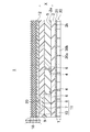
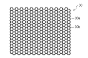
- 1 is a cross-sectional view of an organic EL display device according to a first embodiment of the present invention. It is a top view which shows the structure in the organic electroluminescence display which concerns on the 1st Embodiment of this invention. It is the elements on larger scale of the structure shown in FIG. It is a figure which shows the state which hold
- FIG. 1 is a plan view of an organic EL display device according to the first embodiment of the present invention
- FIG. 2 is a cross-sectional view of the organic EL display device according to the first embodiment of the present invention.
- 3 is a plan view showing a structure in the organic EL display device according to the first embodiment of the present invention
- FIG. 4 is a partially enlarged view of the structure shown in FIG.
- the organic EL display device 1 includes, for example, a display area 32 composed of a plurality of pixels and a peripheral circuit area 48 provided around the display area 32.
- a drive circuit area 34 provided with the driver section 33 and a terminal area 36 provided with wiring terminals 35 drawn out from the display area 32 are defined.
- the organic EL display device 1 includes a film-like organic substrate 2 made of a colorless and transparent resin film deposited at room temperature.
- a material for forming the organic substrate 2 for example, an organic material such as a polyparaxylene resin, an acrylic resin, or a polyimide resin can be used. Note that a metal substrate having flexibility may be used instead of the organic substrate.
- the thickness of the organic substrate 2 is preferably 3 to 20 ⁇ m. This is because if the thickness is less than 3 ⁇ m, sufficient mechanical strength may not be obtained, and if it is greater than 20 ⁇ m, the flexibility of the organic EL display device 1 may be reduced. .
- the gate driver and the source driver corresponding to the driver unit 33 shown in FIG. 1 can be monolithic by adopting a TFT using polysilicon as the TFT element.
- the organic EL display device 1 since the organic substrate 2 of the organic EL display device 1 is formed in a film shape with a polyparaxylene resin or the like, for example, as shown by a dotted frame 37 in FIG. 1. A wide range of areas has good flexibility.
- the flexible region is not limited to the region indicated by the dotted frame 37 in FIG. 1, but can be formed in a desired range by adjusting the configuration of the film substrate.
- the flexible printed wiring board (not shown) connected to the wiring terminals 35, and the flexible printed wiring board is used for driving the organic EL display device 1. It is configured to be connected to an IC unit (not shown).
- a display element layer including a TFT element 4 and the like is formed on the organic substrate 2.
- the display element layer penetrates through the TFT element 4 formed on the organic substrate 2, the interlayer insulating film 5 such as a SiO 2 film or SiN film provided so as to cover the TFT element 4, and the interlayer insulating film 5.
- the metal wiring 6 is electrically connected to the TFT element 4.
- the metal wiring 6 is further extended on the interlayer insulating film 5 to constitute the first electrode 7 of the organic EL display element 11.
- An insulating film (or bank) 9 that partitions each pixel (region) 20 is formed on the interlayer insulating film 5.
- the material for forming the insulating film 9 include insulating resin materials such as photosensitive polyimide resin, acrylic resin, methallyl resin, or novolac resin.
- the thickness of the interlayer insulating film 5 can be set to 0.5 to 1 ⁇ m, for example.
- the thickness of the insulating film 9 can be set to 2 to 4 ⁇ m, for example.
- the organic EL display device 1 is a bottom emission type in which light emission is extracted from the first electrode 7 side
- the first electrode 7 has a high work such as ITO or SnO 2 from the viewpoint of improving the light extraction efficiency. It is preferable to use a thin film of a material having a function and high light transmittance.
- the organic EL layer 8 is formed on the first electrode 7.
- the organic EL layer 8 includes a hole transport layer and a light emitting layer.
- the hole transport layer is not limited as long as the hole injection efficiency is good.
- organic materials such as a triphenylamine inducer, a polyparaphenylene vinylene (PPV) inducer, and a polyfluorene derivative can be used.
- the light emitting layer is not particularly limited, and for example, 8-hydroxyquinolol inducer, thiazole inducer, benzoxazole inducer and the like can be used. Moreover, you may combine 2 or more types among these materials, and may combine additives, such as dopant material.
- the organic EL layer 8 has a two-layer structure of a hole transport layer and a light emitting layer, it is not limited to this configuration. That is, the organic EL layer 8 may have a single layer structure composed of only the light emitting layer. In addition, the organic EL layer 8 may be configured by one or more of a hole transport layer, a hole injection layer, an electron injection layer, and an electron transport layer, and a light emitting layer.
- a second electrode 10 is formed on the organic EL layer 8 and the insulating film 9.
- the second electrode 10 has a function of injecting electrons into the organic EL layer 8.
- the 2nd electrode 10 can be comprised by thin films, such as Mg, Li, Ca, Ag, Al, In, Ce, or Cu, for example, it is not limited to this at all.
- the organic EL display element 11 is formed by the first electrode 7, the organic EL layer 8 having a light emitting layer and the second electrode 10 formed on the organic EL layer 8 while being formed on the first electrode 7. It is configured.
- the first electrode 7 has a function of injecting holes into the organic EL layer 8
- the second electrode 10 has a function of injecting electrons into the organic EL layer 8.
- the holes and electrons injected from the first electrode 7 and the second electrode 10 are recombined in the organic EL layer 8, whereby the organic EL layer 8 emits light.
- the organic substrate 2 and the first electrode 7 are configured to be light transmissive
- the second electrode 10 is configured to be light reflective. Light emission is transmitted through the first electrode 7 and the organic substrate 2 and extracted from the organic EL layer 8. (Bottom emission method).
- planarizing film 12 made of acrylic resin, polyparaxylene resin or the like is formed on the second electrode 10. Note that the thickness of the planarizing film 12 can be set to 3 to 8 ⁇ m, for example.
- a sealing film 18 composed of a laminate of the resin films 13, 15, 17, the inorganic film 14 and the metal oxide film 16 is formed.
- the resin films 13, 15, and 17 may be formed using the same resin material as that of the planarizing film 12, or may be formed using other resin materials.
- the inorganic film 14 and the metal oxide film 16 are formed using, for example, SiNx, SiO 2 or Al 2 O 3 .
- the sealing film 18 does not have to be laminated with multiple layers of resin film and inorganic film as described above, and may be formed one by one. Further, the sealing film 18 may be configured using a metal thin film. The thickness of the sealing film 18 can be set to 1 to 5 ⁇ m, for example.
- the TFT element 4 is a TFT using amorphous silicon, for example, and uses amorphous silicon as a channel. Since this TFT element 4 is amorphous, it has a lower carrier mobility of electrons and the like than a TFT element using polysilicon, but provides a display device having a large screen (that is, a large display region). It becomes possible to do.
- an oxide semiconductor semiconductor layer formed of an IGZO (In—Ga—Zn—O) -based oxide semiconductor film capable of high-speed movement was used instead of the amorphous silicon semiconductor layer.
- a TFT may be used.
- the organic EL display device 1 has a configuration in which the TFT element 4 that is the switching element of the pixel 20 and the organic EL display element 11 are formed on the organic substrate 2 that is a film-like substrate. .
- the honeycomb structure 30 is provided on the surface 2b of the organic substrate 2 opposite to the organic EL display element 11 side.
- a honeycomb structure 30 that improves the rigidity of the organic EL display device 1 is provided on the surface 2b of the organic substrate 2 opposite to the surface 2a on which the organic EL display element 11 is provided.
- a feature in that is a feature in that.
- the rigidity of the organic EL display device 1 can be improved, it is possible to prevent bending due to its own weight, and the organic EL display device 1 can be deformed such as warping and swell. It becomes possible to prevent. Therefore, the display performance of the organic EL display device 1 can be improved.
- the stress 40 can be dispersed by the cell walls 30a of the honeycomb structure 30 as shown in FIG. It becomes possible. That is, since the stress 40 generated at the time of bending is dispersed while propagating through the cell wall 30a, it is possible to prevent stress concentration at a predetermined location of the organic EL display device 1. Accordingly, it is possible to prevent breakage such as cracks in the organic EL display device 1, breakage lines of the metal wiring, and breakage of the TFT element 4, and prevent the yield of the organic EL display device 1 from being lowered. It becomes possible.
- the desired shape can be obtained without causing breakage such as cracks, broken lines of metal wiring, and destruction of the TFT element 4. It can be deformed.
- the honeycomb structure 30 is laminated on the surface 2b of the organic substrate 2 with an adhesive layer 31 interposed therebetween.
- the honeycomb-shaped structure 30 is partitioned by a cell wall (partition wall) 30 a and the cell wall 30 a, and the thickness direction of the honeycomb-shaped structure 30 (that is, organic EL)
- the display device 1 includes a plurality of cells (space portions) 30b penetrating in the thickness direction of the display device 1 (in the direction of arrow X shown in FIG. 2).
- the cell walls 30a of the honeycomb-shaped structure 30 are arranged so as to have a substantially hexagonal cross section as shown in FIGS.
- the cell 30b partitioned by the cell wall 30a has a substantially hexagonal cross section as shown in FIGS.
- the rigidity of the organic EL display device 1 can be improved and flexibility can be imparted to the honeycomb-shaped structure 30. If it is, it will not specifically limit.
- it is formed of a resin material such as polyethylene terephthalate resin, polyethylene naphthalate resin, acrylic resin, polycarbonate resin, stainless steel, iron, aluminum, titanium, nickel, chromium, molybdenum, tantalum, or an alloy thereof. Metal materials can be used.
- the thickness of the honeycomb structure 30 is preferably 10 ⁇ m to 1 mm, and more preferably 50 ⁇ m to 500 ⁇ m. This is because when the thickness is less than 10 ⁇ m, the rigidity of the organic EL display device 1 may not be sufficiently improved. When the thickness is larger than 1 mm, the thickness and weight of the organic EL display device 1 as a whole are large. This is because the size may increase.
- the thickness of the honeycomb-shaped structure 30 is determined by the usage form of the product in which the honeycomb-shaped structure 30 is used, the Young's modulus, the weight, etc. of the material constituting the honeycomb-shaped structure 30.
- an adhesive agent which comprises the adhesive bond layer 31 does not specifically limit as an adhesive agent which comprises the adhesive bond layer 31
- various resin adhesives such as an epoxy resin type, a butyral resin type, an acrylic resin type, are mentioned, for example. It is done.
- 6 to 13 are cross-sectional views for explaining a method of manufacturing an organic EL display device according to an embodiment of the present invention.
- the manufacturing method shown below is merely an example, and the organic EL display device according to the present invention is not limited to the one manufactured by the method shown below.
- a glass substrate 50 having a thickness of about 0.7 mm is prepared as a support substrate.
- 51 is formed with a thickness of about 0.1 to 1 ⁇ m, for example.
- a resin material of the sacrificial film 51 that satisfies such conditions for example, a polyimide resin can be used.
- the sacrificial film 51 is for favorably peeling the glass substrate 50.
- a film-like organic substrate 2 made of a transparent resin film is formed on the sacrificial film 51 with a thickness of about 5 ⁇ m, for example.
- the resin material forming the organic substrate polyimide resin, fluorene epoxy resin, and fluorine resin can be used.
- the organic substrate 2 is formed by applying a resin on the surface of the sacrificial film 51.
- the sacrificial film is omitted by forming the organic substrate 2 using the same resin material as that for forming the sacrificial film 51. It is good also as a structure.
- the organic substrate 2 may be bonded to the glass substrate 50.
- a metal film, a semiconductor film, and the like are formed and patterned on the organic substrate 2 to form the TFT element 4 that is the switching element of the pixel 20.
- an interlayer insulating film 5 is formed on the organic substrate 2 on which the TFT element 4 is formed using, for example, a SiO 2 film or a SiN film so as to have a thickness of about 1 to 2 ⁇ m.
- a contact hole is provided from the surface of the interlayer insulating film 5 to the TFT element 4, a metal wiring 6 electrically connected to the TFT element 4 is formed by a transparent conductive material such as ITO, and further, for example, about 150 nm by patterning or the like.
- the first electrode 7 having the thickness is formed.
- an organic EL layer 8 is provided by forming a hole transport layer and a light emitting layer on the first electrode 7.
- a hole transport material paint in which an organic polymer material that is a hole transport material is dissolved or dispersed in a solvent is supplied onto the exposed first electrode 7 by, for example, an inkjet method or the like. .
- a hole transport layer is formed by performing a baking treatment.
- an organic light-emitting material paint in which an organic polymer material that is a light-emitting material is dissolved or dispersed in a solvent is supplied so as to cover the hole transport layer by, for example, an inkjet method.
- a light emitting layer is formed by performing a baking process.
- the second electrode 10 is formed on the insulating film 9 and the organic EL layer 8 by sputtering, etc. using Mg, Li, Ca, Ag, Al, In, Ce, Cu, or the like.
- the thickness of the second electrode 10 is about 150 nm, for example.
- a TEOS film, a SiN film or the like is formed on the second electrode 10, and the surface is polished by chemical mechanical polishing (CMP) or the like to form the planarizing film 12.
- CMP chemical mechanical polishing
- a resin film 13, an inorganic film 14, a resin film 15, a metal oxide film 16, and a resin film 17 are formed in this order on the planarizing film 12, thereby forming a sealing film 18.
- the laminated body 38 is manufactured.
- the resin films 13, 15, and 17 are formed using, for example, polyparaxylene-based resin or the like so as to have a thickness of about 5 ⁇ m.
- the inorganic film 14 and the metal oxide film 16 are formed using SiNx, SiO 2 , Al 2 O 3, or the like, for example, so as to have a thickness of about 500 nm.
- the produced laminate 38 is transferred to a transfer film 39.
- a material which comprises the transfer film 39 the mold release film etc. from which adhesiveness falls by UV or heat processing are mentioned, for example.
- the glass substrate 50 is peeled off by irradiating laser light (arrows in FIG. 10) from the glass substrate 50 side.
- the removal of the glass substrate 50 may not be peeling by laser light irradiation.
- the glass substrate 50 may be removed using a polishing and etching apparatus.
- the sacrificial film 51 exposed by removing the glass substrate 50 is removed by plasma etching.
- the removal of the sacrificial film 51 is not limited to plasma etching, and may be performed by, for example, microwave plasma etching.
- the sacrificial film 51 does not need to be etched.
- a polyethylene terephthalate resin or stainless steel is interposed via an adhesive layer 31.
- the cell wall 30a formed by, for example, is attached to form a honeycomb structure 30 having a thickness of 150 ⁇ m, for example.
- the organic EL display device 1 shown in FIG. 2 can be manufactured.
- the honeycomb structure 30 having a plurality of cells 30b partitioned by the cell walls 30a is provided on the opposite side of the organic substrate 2 from the organic EL display element 11 side. Therefore, since the rigidity of the organic EL display device 1 can be improved, it is possible to prevent bending due to its own weight, and it is possible to prevent the organic EL display device 1 from being deformed such as warpage or swell. It becomes possible. As a result, the display performance of the organic EL display device 1 can be improved.
- the stress 40 can be dispersed by the cell walls 30a of the honeycomb structure 30. Further, it is possible to prevent stress concentration at a predetermined location of the organic EL display device 1. Accordingly, it is possible to prevent breakage such as cracks in the organic EL display device 1, breakage lines of the metal wiring, and breakage of the TFT element 4, and prevent the yield of the organic EL display device 1 from being lowered. It becomes possible.
- the cell wall 30a is formed of a resin material or a metal material. Therefore, the honeycomb structure 30 can be formed from an inexpensive and versatile material.
- the adhesive layer 31 is provided on the surface 2 b of the organic substrate 2, and the honeycomb structure 30 is provided via the adhesive layer 31. Therefore, the honeycomb structure 30 can be provided on the organic substrate 2 with a simple configuration.
- the thickness of the honeycomb-shaped structure 30 is set to 10 ⁇ m to 1 mm. Accordingly, the rigidity of the organic EL display device 1 can be sufficiently improved without increasing the thickness and weight of the entire organic EL display device 1.
- FIG. 14 is a perspective view showing a structure in an organic EL display device according to the second embodiment of the present invention
- FIG. 15 is a perspective view showing an organic EL display device according to the second embodiment of the present invention. It is. Note that the same components as those in the first embodiment are denoted by the same reference numerals, and description thereof is omitted. Also in the present embodiment, an organic EL display device will be described as an example of the display device. The method for manufacturing the organic EL display device is the same as that in the first embodiment, and a detailed description thereof will be omitted here.
- a lattice-like structure 41 is provided instead of the honeycomb-like structure 30 described above.
- the cell wall 42 of the lattice-like structure 41 is orthogonal to the bending direction Y and the first cell wall 42a extending in the bending direction of the organic EL display device 1 (the direction of the arrow Y shown in FIG. 15). It is characterized in that it is composed of a second cell wall 42b extending in the direction (the direction of arrow Z shown in FIG. 15).
- the organic EL display device 1 when the organic EL display device 1 has one bending direction, the second cell wall 42b extending in the direction Z orthogonal to the bending direction Y shown in FIG. That is, it can be easily bent in a bending direction Y) (for example, bent in a roll shape as shown in FIG. 15), and in the direction Z perpendicular to the bending direction Y, the organic EL display device 1 can be bent. Bending can be prevented.
- the first cell wall 42a extending in the bending direction Y improves the self-supporting property of the organic EL display device 1 bent in the bending direction Y, and holds (saves) the bent state of the organic EL display device 1. It becomes possible. As a result, in the organic EL display device 1, it is easy to bend in one direction and it is difficult to bend in multiple directions. Therefore, the user can deform the organic EL display device 1 into a desired shape, and the display performance is excellent. It becomes possible to provide the organic EL display device 1 that is easy for the user to see.
- the flexibility (flexibility) of the organic EL display device 1 in the bending direction Y and the retention of the bent state are adjusted by appropriately changing the material and thickness of each of the first and second cell walls 42a, 42b. can do.
- the flexibility of the organic EL display device 1 in the bending direction Y is changed by changing the distance between the first cell walls 42a (or the distance between the second cell walls 42b) to change the shape of the plurality of cells 30b. It is good also as a structure which adjusts (flexibility) and the retention of a bending state.
- the distance D between the first cell walls 42a can be increased as compared to the state shown in FIG.
- the cell wall 42 includes a first cell wall 42 a extending in the bending direction Y and a second cell wall 42 b extending in the direction Z orthogonal to the bending direction Y. is doing. Accordingly, the second cell wall 42b allows the user to bend the organic EL display device 1 in a desired direction in a deformable manner. Further, the first cell wall 42a can improve the self-supporting property of the organic EL display device 1 bent in the bending direction Y, and can hold (save) the bent state of the organic EL display device 1. As a result, it is possible to provide the organic EL display device 1 that has excellent display performance and is easy for the user to see.
- FIG. 18 is a plan view showing the overall configuration of a liquid crystal display device according to the third embodiment of the present invention
- FIG. 19 is a cross-sectional view of the liquid crystal display device according to the third embodiment of the present invention.
- FIG. 20 is an equivalent circuit diagram of the liquid crystal display device according to the third embodiment of the present invention
- FIG. 21 is the entire TFT substrate constituting the liquid crystal display device according to the third embodiment of the present invention. It is sectional drawing which shows a structure.
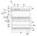
- FIG. 22 is a cross-sectional view showing the overall configuration of the display unit of the liquid crystal display device according to the third embodiment of the present invention.
- a liquid crystal display device will be described as an example of the display device.
- the liquid crystal display device 70 includes a TFT substrate 52 that is a first substrate and a CF substrate 53 that is a second substrate disposed to face the TFT substrate 52.
- the liquid crystal display device 70 is sandwiched between the TFT substrate 52 and the CF substrate 53, and the liquid crystal layer 54, which is a display medium layer sandwiched between the TFT substrate 52 and the CF substrate 53.
- the substrate 52 and the CF substrate 53 are bonded to each other and a sealing material 80 provided in a frame shape is provided to enclose the liquid crystal layer 54.
- the sealing material 80 is formed so as to go around the liquid crystal layer 54, and the TFT substrate 52 and the CF substrate 53 are bonded to each other via the sealing material 80.
- the liquid crystal display device 70 includes a plurality of photo spacers (not shown) for regulating the thickness of the liquid crystal layer 54 (that is, the cell gap).
- the liquid crystal display device 70 is formed in a rectangular shape, and in the longitudinal direction A of the liquid crystal display device 70, the TFT substrate 52 protrudes from the CF substrate 53 on the upper side, and the protrusion In the region, a plurality of display wirings such as gate lines and source lines, which will be described later, are drawn out to form a terminal region T.
- a display area D for displaying an image is defined in an area where the TFT substrate 52 and the CF substrate 53 overlap.
- the display area D is configured by arranging a plurality of pixels, which are the minimum unit of an image, in a matrix.
- the sealing material 80 is provided in a rectangular frame shape surrounding the entire periphery of the display area D as shown in FIG.
- the frame width of the sealing material 80 is not particularly limited, but can be set to 0.5 mm or more and 2.0 mm or less, for example.
- the TFT substrate 52 covers an insulating substrate 56 such as a glass substrate, a plurality of gate lines 61 extending in parallel on the insulating substrate 56, and the gate lines 61.
- the gate insulating film 62 is provided.
- the TFT substrate 52 has a plurality of source lines 64 extending in parallel to each other in a direction orthogonal to the gate lines 61 on the gate insulating film 62, and each intersection of the gate lines 61 and the source lines 64.
- a plurality of TFT elements 55 are provided.
- the TFT substrate 52 includes a first interlayer insulating film 65 and a second interlayer insulating film 66 which are interlayer insulating films 60 provided in order so as to cover each source line 64 and each TFT element 55, and a second interlayer insulating film.
- a plurality of pixel electrodes 69 provided in a matrix on 66 and connected to each of the TFT elements 55, and an alignment film 59 provided so as to cover each pixel electrode 69.
- the TFT element 55 includes a gate electrode 67 in which each gate line 61 protrudes sideways, a gate insulating film 62 provided so as to cover the gate electrode 67, and the gate insulating film 62.
- the semiconductor layer 63 is provided in an island shape at a position overlapping the gate electrode 67.
- the TFT element 55 includes a source electrode 68 and a drain electrode 77 provided on the semiconductor layer 63 so as to face each other.
- the source electrode 68 is a portion where each source line 64 protrudes to the side.
- the drain electrode 77 is connected to the pixel electrode 69 via a contact hole 84 formed in the first interlayer insulating film 65 and the second interlayer insulating film 66.
- the pixel electrode 69 includes a transparent electrode 81 provided on the second interlayer insulating film 66, and a reflective electrode that is stacked on the transparent electrode 81 and provided on the surface of the transparent electrode 81. 82.
- the semiconductor layer 63 includes a lower intrinsic amorphous silicon layer 63 a and an upper layer n + amorphous silicon layer 63 b doped with phosphorus, and is exposed from the source electrode 68 and the drain electrode 77.
- the intrinsic amorphous silicon layer 63a that constitutes the channel region.
- the reflective region R is defined by the reflective electrode 82.
- the surface of the second interlayer insulating film 66 under the pixel electrode 69 is formed in an uneven shape, and is provided on the surface of the second interlayer insulating film 66 via the transparent electrode 81.
- the surface of the reflective electrode 82 is also formed in an uneven shape.
- the material forming the first interlayer insulating film 65 is not particularly limited, and examples thereof include silicon oxide (SiO 2 ) and silicon nitride (SiNx (x is a positive number)).
- the thickness of the first interlayer insulating film 65 is preferably 600 nm or more and 1000 nm or less. This is because when the thickness of the first interlayer insulating film 65 is less than 600 nm, it may be difficult to planarize the first interlayer insulating film 65. When the thickness is larger than 1000 nm, This is because there is a case where it becomes difficult to form the contact hole 84 by etching.
- the CF substrate 53 is provided so as to cover an insulating substrate 71 such as a glass substrate, a color filter 72 provided on the insulating substrate 71, and a reflection region R of the color filter 72. It has a common electrode 74, a photo spacer (not shown) provided in a column shape on the common electrode 74, and an alignment film 76 provided so as to cover the common electrode 74 and the photo spacer.
- the color filter 72 includes a plurality of types of colored layers 78 (that is, a red layer R, a green layer G, and a blue layer B) provided for each pixel, and a light shielding film.
- a certain black matrix 83 is included.
- the black matrix 83 is provided between adjacent colored layers 78 and has a role of partitioning the plurality of types of colored layers 78.
- the black matrix 83 is made of a metal material such as Ta (tantalum), Cr (chromium), Mo (molybdenum), Ni (nickel), Ti (titanium), Cu (copper), Al (aluminum), or a black pigment such as carbon.
- a metal material such as Ta (tantalum), Cr (chromium), Mo (molybdenum), Ni (nickel), Ti (titanium), Cu (copper), Al (aluminum), or a black pigment such as carbon.
- the photo spacer is made of, for example, an acrylic photosensitive resin, and is formed by a photolithography method.
- the liquid crystal display element 85 is configured by the pixel electrode 69, the liquid crystal layer 54 formed in a pixel electrode shape, and the common electrode 74 formed on the liquid crystal layer 54.
- the reflection type liquid crystal display device 70 having the above-described configuration is configured such that light incident from the CF substrate 53 side in the reflection region R is reflected by the reflection electrode 82.
- the liquid crystal display device 70 one pixel is formed for each pixel electrode 69.
- the source line A source signal is sent from 64 and a predetermined charge is written into the pixel electrode 69 through the source electrode 68 and the drain electrode 77.
- a potential difference is generated between the pixel electrode 69 and the common electrode 74, and a predetermined voltage is applied to the liquid crystal layer 54.
- the reflectance of light incident from the CF substrate 53 side is adjusted by utilizing the change in the alignment state of the liquid crystal molecules according to the magnitude of the applied voltage. Is displayed.
- the side opposite to the liquid crystal display element 85 side in the insulating substrate 56 is characterized in that a honeycomb-like structure 30 is provided on the surface 56b.
- the honeycomb structure 30 for improving the rigidity of the liquid crystal display device 70 is provided on the surface 56b of the insulating substrate 56 opposite to the surface 56a on which the liquid crystal display element 85 is provided.
- the honeycomb structure 30 is configured such that the adhesive layer 31 is provided on the surface 56 b of the insulating substrate 56 and is provided via the adhesive layer 31.
- the same effects as the above (1) to (4) can be obtained. That is, since the rigidity of the liquid crystal display device 70 can be improved, it is possible to prevent bending due to its own weight, and it is possible to prevent the liquid crystal display device 70 from being deformed such as warpage or swell. Become. Therefore, the display performance of the liquid crystal display device 70 can be improved.
- the liquid crystal display device 70 since it is possible to prevent bending due to its own weight, even when the end of the liquid crystal display device 70 is gripped, it is self-supporting with respect to the support at the end (that is, it does not bend and does not deform). The independence of the display device 70 can be improved.
- the stress 40 can be dispersed by the cell walls 30a of the honeycomb structure 30. It becomes possible to prevent the concentration of stress at 70 predetermined locations. Accordingly, it is possible to prevent breakage such as cracks in the liquid crystal display device 70, breakage lines of the metal wiring, and breakage of the TFT element 55, and it is possible to prevent the yield of the liquid crystal display device 70 from being lowered. Become.
- the desired shape can be obtained without causing breakage such as cracks, broken lines of metal wiring, and destruction of the TFT element 55. It can be deformed.
- the honeycomb structure 30 including the cells 30b having the substantially hexagonal cross section which is arranged so that the cell wall 30a has the substantially hexagonal cross section is defined.
- the arrangement of the cell walls 30a and the cross-sectional shape of the cells 30b can be appropriately changed.
- a structure 43 having a cell 43b having a substantially circular cross-section partitioned by the cell wall 43a and having a cell wall 43a having a substantially circular cross-section is used. It is good also as a structure.
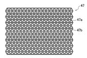
- a cell body 47a is arranged so as to have a substantially triangular cross section, and a structure 47 including a cell 47b having a substantially triangular cross section partitioned by the cell wall 47a is provided. It is good also as a structure to use.
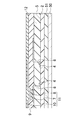
- a honeycomb structure 30 is covered with a coat layer 45, and a laminate structure including the honeycomb structure 30 and the coat layer 45 is formed. 46 may be laminated on the surface 2 b of the organic substrate 2 via the adhesive layer 31. With such a configuration, it is possible to effectively prevent the organic substrate 2 to which the honeycomb structure 30 is attached from being damaged.
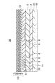
- the honeycomb structure 30 is covered with the coat layer 45, and the laminate structure 46 including the honeycomb structure 30 and the coat layer 45 is replaced with the insulating substrate 56. It is good also as a structure laminated
- an epoxy resin can be used as a material for forming the coat layer 45 .
- a method of forming the coat layer 45 for example, a method of coating an epoxy resin on the surface of the honeycomb structure 30 by a CVD method can be employed.
- the laminate structure 46 can be formed by attaching a sheet-like coat layer 45 formed of PET (polyethylene terephthalate) or PEN (polyethylene naphthalate) to the surface of the honeycomb-like structure 30.
- the thickness of the coat layer 45 can be set to 300 ⁇ m, for example.
- the structure 41 described in the above second embodiment may be used instead of the honeycomb structure 30.
- the cell wall 42 of the structure 41 includes a first cell wall 42a extending in the bending direction of the liquid crystal display device 70 and a second cell wall 42b extending in a direction orthogonal to the bending direction. Will be. With such a configuration, the same effect as the above (8) can be obtained.
- a TFT using amorphous silicon is used as the TFT element 4.
- a TFT element using a zinc oxide based semiconductor as a channel a TFT element using an organic semiconductor as a channel, A TFT element using a carbon nanotube as a channel may be used. With such a configuration, it is possible to form the TFT element 4 capable of increasing the screen size by using a versatile material as in the case of using a TFT using amorphous silicon as the TFT element 4.
- the display device related to organic EL (organic electro luminescence) and LCD (liquid crystal display) has been shown.
- the display device includes electrophoresis (electrophoretic), PD (plasma display); Plasma display), PALC (plasma addressed liquid crystal display), inorganic EL (inorganic electroluminescence), FED (field emission display), or SED (surface-conduction electron-emitter display) Electric field display) or the like.
- the present invention is useful for display devices such as organic EL display devices having flexibility.
Landscapes
- Physics & Mathematics (AREA)
- Engineering & Computer Science (AREA)
- Manufacturing & Machinery (AREA)
- Nonlinear Science (AREA)
- Optics & Photonics (AREA)
- Mathematical Physics (AREA)
- Chemical & Material Sciences (AREA)
- Crystallography & Structural Chemistry (AREA)
- General Physics & Mathematics (AREA)
- Electroluminescent Light Sources (AREA)
- Devices For Indicating Variable Information By Combining Individual Elements (AREA)
Abstract
有機EL表示装置(1)は、有機基板(2)と、有機基板(2)上に形成された有機EL表示素子(11)とを備えている。そして、有機基板(2)における有機EL表示素子(11)側とは反対側に、セル壁(30a)によって区画された複数のセル(30b)を有するハニカム状の構造体(30)が設けられている。
Description
本発明は、有機EL表示装置等の表示装置に関する。
近年、ディスプレイ分野では、フレキシブル性、耐衝撃性や軽量性の点でガラス基板に比べて大きなメリットのある有機基板等を用いた薄型の表示装置が非常に注目を浴びており、ガラス基板のディスプレイでは不可能であった新たなディスプレイが創出される可能性を秘めている。
例えば、第1の方向に延在するとともに第2の方向に配列するデータ線と、第2の方向に延在するとともに第1の方向に配列したセレクト線と、データ線とセレクト線とで囲まれた領域にTFTと有機EL層が形成されたTFT基板を備え、上述の第2の方向に湾曲することが可能な有機EL表示装置が開示されている(例えば、特許文献1参照)。
ここで、一般に、上記特許文献1に記載の有機EL表示装置のような表示装置においては、ポリイミド樹脂等により形成された厚みの薄い(例えば、100μm程度)フィルム基材を備えており、フレキシブル性を有するが、当該フレキシブル性が高いと自重により撓んでしまい、表示装置に反りやうねり等の変形が発生する。その結果、表示が見えにくくなるという問題があった。
また、フレキシブル性が高いと、機械的なストレス等の外力により表示装置が屈曲する。そうすると、当該屈曲に起因して、表示装置の所定箇所に応力が集中してしまい、表示装置にクラック等の破損、金属配線の破断線、TFT素子の破壊が発生するという問題があった。また、特に、製造工程において、このようなクラックが発生すると、表示装置の歩留まりが低下するという問題が生じていた。
そこで、本発明は、上述の問題に鑑みてなされたものであり、フレキシブル性を有するとともに良好な表示性能を有し、屈曲に起因するクラック等の破損、金属配線の破断線、TFT素子の破壊の発生を抑制して、歩留まりを向上することができる表示装置を提供することを目的とする。
上記目的を達成するために、本発明の表示装置は、基板と、基板上に形成された表示素子とを備え、基板における表示素子側とは反対側に、セル壁によって区画された複数のセルを有する構造体が設けられていることを特徴とする。
同構成によれば、表示装置の剛性を向上させることができるため、自重による撓みを防止することが可能になり、表示装置に反りやうねり等の変形が発生するのを防止することが可能になる。従って、表示装置の表示性能を向上させることができる。
また、自重による撓みを防止することができるため、表示装置の端部を把持した場合であっても、端部における支持に対して自立し、表示装置の自立性を向上させることができる。
また、機械的なストレス等の外力により表示装置が屈曲した場合であっても、構造体のセル壁により、応力を分散することができ、表示装置の所定箇所における応力の集中を防止することが可能になる。従って、表示装置におけるクラック等の破損、金属配線の破断線、TFT素子の破壊の発生を防止することが可能になるとともに、表示装置の歩留まりの低下を防止することが可能になる。
更に、ユーザーが意図的に表示装置に対して応力を加えた場合であっても、クラック等の破損、金属配線の破断線、TFT素子の破壊を生じることなく、所望の形状に変形させることが可能になる。
また、本発明の表示装置においては、セル壁が、樹脂材料または金属材料により形成されていてもよい。
同構成によれば、安価かつ汎用性のある材料により、構造体を形成することが可能になる。
また、本発明の表示装置においては、基板の表面上に接着剤層が設けられ、構造体が、接着剤層を介して設けられていてもよい。
同構成によれば、簡単な構成で、基板に構造体を設けることが可能になる。
また、本発明の表示装置においては、構造体の厚みが、10μm~1mmであってもよい。
同構成によれば、表示装置全体の厚み及び重みを大きくすることなく、表示装置の剛性を十分に向上させることができる。
また、本発明の表示装置においては、構造体が、コート層により被覆されていてもよい。
同構成によれば、構造体が取り付けられた有機基板の破損を効果的に防止することが可能になる。
また、本発明の表示装置においては、セル壁が、表示装置の屈曲方向に延設された第1セル壁と、屈曲方向と直交する方向に延設された第2セル壁とから構成されていてもよい。
同構成によれば、表示装置の屈曲方向が1方向の場合、第2セル壁により、ユーザーが所望の方向に変形自在に屈曲(例えば、ロール状に屈曲)させることができるとともに、第1セル壁により、表示装置の屈曲状態を保持することが可能になる。従って、表示性能に優れた、ユーザーが見易い表示装置を提供することが可能になる。
また、本発明の表示装置は、表示装置の表示性能を向上させることができるとともに、クラック等の破損、金属配線の破断線、TFT素子の破壊の発生を防止して、表示装置の歩留まりの低下を防止することができるという優れた特性を備えている。従って、本発明は、表示素子に、有機EL表示素子を使用した表示装置に好適に使用できる。また、本発明は、表示素子に、液晶表示素子を使用した表示装置に好適に使用できる。
本発明によれば、フレキシブル性を有するとともに良好な表示性能を有し、薄さ・軽さを損なわずに、屈曲に起因するクラック等の破損、金属配線の破断線、TFT素子の破壊の発生を効果的に抑制して、歩留まりを向上することができる表示装置を提供することが可能になる。
(第1の実施形態)
以下、本発明の実施形態に係る表示装置を図面に基づいて詳細に説明する。尚、本発明は、以下の実施形態に限定されるものではない。また、本実施形態においては、表示装置として、有機EL表示装置を例に挙げて説明する。
以下、本発明の実施形態に係る表示装置を図面に基づいて詳細に説明する。尚、本発明は、以下の実施形態に限定されるものではない。また、本実施形態においては、表示装置として、有機EL表示装置を例に挙げて説明する。
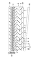
図1は、本発明の第1の実施形態に係る有機EL表示装置の平面図であり、図2は、本発明の第1の実施形態に係る有機EL表示装置の断面図である。また、図3は、本発明の第1の実施形態に係る有機EL表示装置における構造体を示す平面図であり、図4は、図3に示す構造体の部分拡大図である。
図1に示すように、有機EL表示装置1は、例えば、複数の画素等で構成される表示領域32と表示領域32の周辺に設けられた周辺回路領域48とを備えている。
また、周辺回路領域48には、ドライバ部33が設けられた駆動回路領域34と、表示領域32から引き出された配線端子35が設けられた端子領域36が規定されている。
また、有機EL表示装置1は、室温で蒸着された無色透明の樹脂膜で構成されたフィルム状の可撓性(フレキシビリティー)を有する有機基板2を備える。この有機基板2を形成する材料としては、例えば、ポリパラキシレン系樹脂、アクリル系樹脂、ポリイミド系樹脂等の有機材料を用いることができる。なお、有機基板の代わりに、可撓性を有する金属基板を使用する構成としても良い。
また、有機基板2の厚みとしては、3~20μmが好ましい。これは、厚みが3μm未満の場合は、十分な機械的強度が得られない場合があり、また、20μmよりも大きい場合は、有機EL表示装置1の柔軟性が低下する場合があるからである。
また、図1に示すドライバ部33にあたるゲートドライバやソースドライバは、TFT素子としてポリシリコンを用いたTFTを採用することによりモノリシック化が可能である。また、有機EL表示装置1は、上述のごとく、有機EL表示装置1の有機基板2がポリパラキシレン系樹脂等でフィルム状に形成されているため、例えば、図1の点線枠37に示すような広範囲な領域が良好なフレキシブル性を有している。
また、フレキシブルな領域は、図1の点線枠37で示す領域に限らず、フィルム基板の構成等を調節することにより、所望の範囲に形成することができる。
なお、図1に示す端子領域36には、配線端子35に接続されたフレキシブルプリント配線板(不図示)が設けられており、当該フレキシブルプリント配線板が、有機EL表示装置1を駆動するためのIC部(不図示)と接続される構成となっている。
また、図2に示すように、本実施形態の有機EL表示装置1においては、有機基板2上には、TFT素子4等を備えた表示素子層が形成されている。この表示素子層は、有機基板2上に形成されたTFT素子4と、TFT素子4を覆うように設けられたSiO2膜やSiN膜等の層間絶縁膜5と、層間絶縁膜5を貫通してTFT素子4に電気的に接続されたメタル配線6により構成されている。
メタル配線6は、さらに層間絶縁膜5上に延長されて、有機EL表示素子11の第1電極7を構成している。
また、層間絶縁膜5上には、各画素(領域)20を区画する絶縁膜(または、バンク)9が形成されている。この絶縁膜9を形成する材料としては、例えば、感光性ポリイミド樹脂、アクリル系樹脂、メタリル系樹脂、またはノボラック系樹脂等の絶縁性の樹脂材料が挙げられる。なお、層間絶縁膜5の厚みは、例えば、0.5~1μmとすることができる。また、絶縁膜9の厚みは、例えば、2~4μmとすることができる。
有機EL表示装置1は、第1電極7側から発光を取り出すボトムエミッション型であるため、発光の取り出し効率を向上する観点から、第1電極7は、例えば、ITOや、SnO2等の高い仕事関数を有し、かつ、光透過率の高い材料の薄膜により構成することが好ましい。
第1電極7上には、有機EL層8が形成されている。有機EL層8は、ホール輸送層と発光層とからなる。ホール輸送層は、ホール注入効率がよいものであれば、何ら限定されるものではない。ホール輸送層の材料としては、例えば、トリフェニルアミン誘動体、ポリパラフェニレンビニレン(PPV)誘動体、ポリフルオレン誘導体などの有機材料等を用いることができる。
発光層は、特に限定されるものではなく、例えば、8-ヒドロキシキノリロール誘動体、チアゾール誘動体、ベンズオキサゾール誘動体等を用いることができる。また、これらの材料のうち2種以上を組み合わせたり、ドーパント材料などの添加剤を組み合わせてもよい。
なお、有機EL層8をホール輸送層と発光層との2層構造としているが、何らこの構成に限定されるものではない。即ち、有機EL層8は、発光層のみからなる単層構造であっても構わない。また、有機EL層8を、ホール輸送層、ホール注入層、電子注入層、及び、電子輸送層のうちの1層または2層以上と、発光層とにより構成してもよい。
また、有機EL層8及び絶縁膜9上には、第2電極10が形成されている。第2電極10は、有機EL層8に電子を注入する機能を有する。第2電極10は、例えば、Mg、Li、Ca、Ag、Al、In、Ce又はCu等の薄膜により構成することができるが、何らこれに限定されるものではない。
そして、第1電極7と、第1電極7上に形成されるとともに、発光層を有する有機EL層8と、有機EL層8上に形成された第2電極10とにより有機EL表示素子11が構成されている。
また、有機EL表示装置1では、第1電極7は有機EL層8にホールを注入する機能を有し、また、第2電極10は有機EL層8に電子を注入する機能を有する。第1電極7と、第2電極10とからそれぞれ注入されたホールと電子とが有機EL層8で再結合することにより、有機EL層8が発光する仕組みとなっている。また、有機基板2及び第1電極7は光透過性に、第2電極10は光反射性に構成されており、発光は第1電極7及び有機基板2を透過して有機EL層8から取り出される仕組みとなっている(ボトムエミッション方式)。
また、第2電極10上には、アクリル樹脂やポリパラキシレン樹脂等からなる平坦化膜12が形成されている。なお、平坦化膜12の厚みは、例えば、3~8μmとすることができる。
平坦化膜12上には、樹脂膜13,15,17、無機膜14及び金属酸化膜16の積層体により構成された封止膜18が形成されている。樹脂膜13,15,17は、平坦化膜12と同様の樹脂材料を用いて形成しても良く、その他の樹脂材料を用いて形成しても良い。無機膜14及び金属酸化膜16は、例えば、SiNx、SiO2又はAl2O3等を用いて形成されている。
なお、封止膜18は、樹脂膜と無機膜とが上記のように何重にも積層されていなくても良く、それぞれ1層ずつ形成されていても良い。さらに、封止膜18は、金属薄膜を用いて構成しても良い。また、封止膜18の厚みは、例えば、1~5μmとすることができる。
また、TFT素子4は、例えば、アモルファスシリコンを用いたTFTであり、アモルファスシリコンをチャネルとするものである。このTFT素子4は、非晶質であるために、ポリシリコンを用いたTFT素子に比し、電子等のキャリア移動度が低いが、大画面(即ち、大きな表示領域)を有する表示装置を提供することが可能になる。
なお、TFT素子4として、アモルファスシリコンの半導体層の代わりに、高速移動が可能なIGZO(In-Ga-Zn-O)系の酸化物半導体膜により形成された酸化物半導体の半導体層を用いたTFTを使用しても良い。
このように、有機EL表示装置1は、フィルム状の基板である有機基板2上に、画素20のスイッチング素子であるTFT素子4と、有機EL表示素子11とが形成された構成となっている。
ここで、本実施形態の有機EL表示装置1においては、図2に示すように、有機基板2における有機EL表示素子11側とは反対側の表面2b上にハニカム状の構造体30を備える点に特徴がある。より具体的には、有機基板2の、有機EL表示素子11が設けられた表面2aと反対側の表面2b上に、有機EL表示装置1の剛性を向上するハニカム状の構造体30を設けている点に特徴がある。
このような構成により、有機EL表示装置1の剛性を向上させることができるため、自重による撓みを防止することが可能になり、有機EL表示装置1に反りやうねり等の変形が発生するのを防止することが可能になる。従って、有機EL表示装置1の表示性能を向上させることができる。
また、自重による撓みを防止することができるため、図5に示す様に、有機EL表示装置1の端部を把持した場合であっても、端部における支持に対して自立する(即ち、撓まず、変形しない)ため、有機EL表示装置1の自立性を向上させることができる。
また、機械的なストレス等の外力により有機EL表示装置1が屈曲した場合であっても、図4に示すように、ハニカム状の構造体30のセル壁30aにより、応力40を分散することが可能になる。即ち、屈曲時に発生した応力40が、セル壁30aを伝搬しながら分散されていくため、有機EL表示装置1の所定箇所における応力の集中を防止することが可能になる。従って、有機EL表示装置1におけるクラック等の破損、金属配線の破断線、TFT素子4の破壊の発生を防止することが可能になるとともに、有機EL表示装置1の歩留まりが低下を防止することが可能になる。
また、ユーザーが意図的に有機EL表示装置1に対して応力を加えた場合であっても、クラック等の破損、金属配線の破断線、TFT素子4の破壊を生じることなく、所望の形状に変形させることが可能になる。
このハニカム状の構造体30は、図2に示すように、有機基板2の表面2bにおいて、接着剤層31を介して、積層される構成となっている。
また、図2、図3に示すように、ハニカム状の構造体30は、セル壁(隔壁)30aと、当該セル壁30aにより区画され、ハニカム状の構造体30の厚み方向(即ち、有機EL表示装置1の厚み方向であって、図2に示す矢印Xの方向)に貫通する複数のセル(空間部)30bとを備えている。
また、本実施形態においては、ハニカム状の構造体30のセル壁30aは、図3、図4に示すように、断面略六角形状となるように配置されている。また、同様に、セル壁30aにより区画されたセル30bは、図3、図4に示すように、断面略六角形状を有している。
また、ハニカム状の構造体30のセル壁30aを形成する材料としては、有機EL表示装置1の剛性を向上することができるとともに、ハニカム状の構造体30にフレキシブル性を付与することができるものであれば特に限定されない。本実施形態においては、ポリエチレンテレフタラート樹脂、ポリエチレンナフタレート樹脂、アクリル樹脂、ポリカーボネート樹脂等の樹脂材料や、ステンレス、鉄、アルミニウム、チタン、ニッケル、クロム、モリブテン、タンタルまたはこれらの合金により形成された金属材料を使用することができる。
また、ハニカム状の構造体30の厚みとしては、10μm~1mmが好ましく、50μm~500μmが更に好ましい。これは、厚みが10μm未満の場合は、有機EL表示装置1の剛性を十分に向上できない場合があるからであり、また、1mmよりも大きい場合は、有機EL表示装置1全体の厚みと重みが大きくなる場合があるからである。
なお、ハニカム状の構造体30の厚みは、ハニカム状の構造体30が使用される商品の使用形態やハニカム状の構造体30を構成する材料のヤング率や重量等によって決定される。
また、接着剤層31を構成する接着剤としては、特に限定されず、かかる接着剤としては、例えば、エポキシ樹脂系、ブチラール樹脂系、アクリル樹脂系などの、各種の樹脂系の接着剤が挙げられる。
次に、本発明の実施形態に係る有機EL表示装置の製造方法について説明する。図6~図13は、本発明の実施形態に係る有機EL表示装置の製造方法を説明するための断面図である。なお、以下に示す製造方法は単なる例示であり、本発明に係る有機EL表示装置は以下に示す方法により製造されたものに限定されるものではない。
まず、図6に示すように、支持基板として、例えば、厚みが0.7mm程度のガラス基板50を準備する。
次に、図6に示すように、ガラス基板50上に、例えば、耐熱温度(又は、ガラス転移温度)が400℃以上で、熱膨張係数が10ppm/℃以下の樹脂材料で形成された犠牲膜51を、例えば、0.1~1μm程度の厚みで形成する。このような条件を満たす犠牲膜51の樹脂材料としては、例えば、ポリイミド系樹脂を用いることができる。なお、この犠牲膜51は、ガラス基板50の剥離を良好に行うためのものである。
次いで、透過型の表示素子の場合は、犠牲膜51上に、透明の樹脂膜で構成されたフィルム状の有機基板2を、例えば、5μm程度の厚みで形成する。有機基板2を形成する樹脂材料としては、ポリイミド系樹脂、フルオレン系エポキシ樹脂及びフッ素系樹脂を用いることができる。また、本実施形態においては、有機基板2は、犠牲膜51の表面上に樹脂を塗布することにより形成する。なお、反射型の表示素子の場合やトップエミッション自発光型の表示素子の場合は、犠牲膜51を形成する樹脂材料と同じ樹脂材料を用いて有機基板2を形成することにより、犠牲膜を省く構成としても良い。また、有機基板2をガラス基板50に接着する構成としても良い。
次いで、図7に示すように、有機基板2上に、金属膜や半導体膜等の形成、及びパターニング等を行い、画素20のスイッチング素子であるTFT素子4を形成する。
次に、TFT素子4を形成した有機基板2上に、例えば、SiO2膜やSiN膜等を用いて、層間絶縁膜5を、厚みが1~2μm程度となるように形成する。
次いで、層間絶縁膜5の表面からTFT素子4までコンタクトホールを設け、ITO等の透明導電材料によってTFT素子4と電気的に接続するメタル配線6を形成し、さらにパターニング等によって、例えば、150nm程度の厚みを有する第1電極7を形成する。
次に、層間絶縁膜5上に、例えば、3μm程度の厚みを有する絶縁膜9を形成後、第1電極7に対応する部分をエッチングにより除去する。
次いで、第1電極7上にホール輸送層と発光層とを形成することにより、有機EL層8を設ける。ホール輸送層としては、まず、溶剤にホール輸送材料である有機高分子材料を溶解、または分散させたホール輸送材料塗料を、例えば、インクジェット法等により露出している第1電極7上に供給する。その後、焼成処理を施すことによりホール輸送層を形成する。次に、発光層としては、溶剤に発光材料である有機高分子材料を溶解、または分散させた有機発光材料塗料を、例えば、インクジェット法等によりホール輸送層を覆うように供給する。その後、焼成処理を施すことにより発光層を形成する。
次いで、絶縁膜9及び有機EL層8上に、スパッタ法等によりMg、Li、Ca、Ag、Al、In、Ce、またはCu等を用いて第2電極10を形成する。第2電極10の厚みは、例えば150nm程度とする。これにより、第1電極7と、第1電極7上に形成されるとともに、発光層を有する有機EL層8と、有機EL層8上に形成された第2電極10とにより構成される有機EL表示素子11が形成される。
次に、第2電極10上に、TEOS膜やSiN膜等を成膜し、化学機械研磨(CMP)等により表面を研磨することにより平坦化膜12を形成する。
次いで、図8に示すように、平坦化膜12上に、樹脂膜13、無機膜14、樹脂膜15、金属酸化膜16及び樹脂膜17をこの順で成膜することにより封止膜18を形成して、積層体38を作製する。樹脂膜13,15,17は、例えば、ポリパラキシレン系樹脂等を用いて、厚みがそれぞれ5μm程度となるように形成する。また、無機膜14及び金属酸化膜16は、例えば、SiNx、SiO2、Al2O3等を用いて、厚みがそれぞれ500nm程度となるように形成する。
次いで、図9に示すように、作製した積層体38を転写フィルム39に転写する。なお、転写フィルム39を構成する材料としては、例えば、UVや熱処理により密着性が低下する離形フィルム等が挙げられる。
次いで、図10に示すように、ガラス基板50側からレーザ光(図10における矢印)を照射することにより、ガラス基板50を剥離させる。
ここで、ガラス基板50の除去は、レーザ光照射による剥離でなくてもよい。例えば、研磨及びエッチング装置を用いてガラス基板50を除去してもよい。
次に、図11に示すように、ガラス基板50を除去したことにより剥き出しとなった犠牲膜51をプラズマエッチングにより除去する。ここで、犠牲膜51の除去は、プラズマエッチングに限らず、例えば、マイクロ波プラズマエッチングにより行ってもよい。なお、反射型の表示素子の場合やトップエミッション自発光型の表示素子の場合は、犠牲膜51をエッチングする必要はない。
次に、図12に示すように、有機基板2の、有機EL表示素子11が設けられた表面2aと反対側の表面2b上に、接着剤層31を介して、ポリエチレンテレフタラート樹脂や、ステンレス等により形成されたセル壁30aを貼り付けて、例えば、150μmの厚みを有するハニカム状の構造体30を形成する。
次いで、図13に示すように、封止膜18の表面から転写フィルム39を剥離することにより、図2に示す有機EL表示装置1を製造することができる。
以上に説明した本実施形態によれば、以下の効果を得ることができる。
(1)本実施形態においては、有機基板2における有機EL表示素子11側とは反対側に、セル壁30aによって区画された複数のセル30bを有するハニカム状の構造体30を設ける構成としている。従って、有機EL表示装置1の剛性を向上させることができるため、自重による撓みを防止することが可能になり、有機EL表示装置1に反りやうねり等の変形が発生するのを防止することが可能になる。その結果、有機EL表示装置1の表示性能を向上させることができる。
(2)また、自重による撓みを防止することができるため、有機EL表示装置1の自立性を向上させることができる。
(3)また、機械的なストレス等の外力により有機EL表示装置1が屈曲した場合であっても、ハニカム状の構造体30のセル壁30aにより、応力40を分散することが可能になるため、有機EL表示装置1の所定箇所における応力の集中を防止することが可能になる。従って、有機EL表示装置1におけるクラック等の破損、金属配線の破断線、TFT素子4の破壊の発生を防止することが可能になるとともに、有機EL表示装置1の歩留まりが低下を防止することが可能になる。
(4)更に、ユーザーが意図的に有機EL表示装置1に対して応力を加えた場合であっても、クラック等の破損、金属配線の破断線、TFT素子4の破壊を生じることなく、所望の形状に変形させることが可能になる。
(5)本実施形態においては、セル壁30aを、樹脂材料または金属材料により形成する構成としている。従って、安価かつ汎用性のある材料により、ハニカム状の構造体30を形成することが可能になる。
(6)本実施形態においては、有機基板2の表面2b上に接着剤層31を設け、ハニカム状の構造体30を、接着剤層31を介して設ける構成としている。従って、簡単な構成で、有機基板2にハニカム状の構造体30を設けることが可能になる。
(7)本実施形態においては、ハニカム状の構造体30の厚みを、10μm~1mmに設定する構成としている。従って、有機EL表示装置1全体の厚み及び重みを大きくすることなく、有機EL表示装置1の剛性を十分に向上させることができる。
(第2の実施形態)
次に、本発明の第2の実施形態について説明する。図14は、本発明の第2の実施形態に係る有機EL表示装置における構造体を示す斜視図であり、図15は、本発明の第2の実施形態に係る有機EL表示装置を示す斜視図である。なお、上記第1の実施形態と同様の構成部分については同一の符号を付してその説明を省略する。また、本実施形態においても、表示装置として、有機EL表示装置を例に挙げて説明する。また、有機EL表示装置の製造方法は、上記第1の実施形態と同様であるため、ここでは詳しい説明を省略する。
次に、本発明の第2の実施形態について説明する。図14は、本発明の第2の実施形態に係る有機EL表示装置における構造体を示す斜視図であり、図15は、本発明の第2の実施形態に係る有機EL表示装置を示す斜視図である。なお、上記第1の実施形態と同様の構成部分については同一の符号を付してその説明を省略する。また、本実施形態においても、表示装置として、有機EL表示装置を例に挙げて説明する。また、有機EL表示装置の製造方法は、上記第1の実施形態と同様であるため、ここでは詳しい説明を省略する。
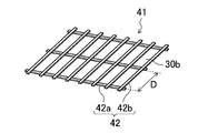
本実施形態においては、図14、図15に示すように、上述のハニカム状の構造体30の代わりに格子状の構造体41が設けられている。そして、格子状の構造体41のセル壁42が、有機EL表示装置1の屈曲方向(図15に示す矢印Yの方向)に延設された第1セル壁42aと、屈曲方向Yと直交する方向(図15に示す矢印Zの方向)に延設された第2セル壁42bとから構成されている点に特徴がある。
このような構成により、有機EL表示装置1の屈曲方向が1方向の場合、図15に示す屈曲方向Yと直交する方向Zに延設された第2セル壁42bにより、ユーザーが所望の方向(即ち、屈曲方向Y)に変形自在に屈曲(例えば、図15に示すようなロール状に屈曲)させ易くすることができるとともに、屈曲方向Yと直交する方向Zにおいては、有機EL表示装置1の屈曲を防止することができる。
また、屈曲方向Yに延設された第1セル壁42aにより、屈曲方向Yに屈曲した有機EL表示装置1の自立性を向上させて、有機EL表示装置1の屈曲状態を保持(保存)することが可能になる。その結果、有機EL表示装置1において、1方向に屈曲させ易く、多方向には屈曲させ難くなるため、有機EL表示装置1をユーザーが所望の形状に変形させることができ、表示性能に優れた、ユーザーが見易い有機EL表示装置1を提供することが可能になる。
なお、第1及び第2セル壁42a,42bの各々の材質や厚みを適宜変更することにより、屈曲方向Yにおける有機EL表示装置1のフレキシブル性(屈曲性)と屈曲状態の保持性とを調整することができる。
また、第1セル壁42a間の距離(または、第2セル壁42b間の距離)を変更して複数のセル30bの形状を変更することにより、屈曲方向Yにおける有機EL表示装置1のフレキシブル性(屈曲性)と屈曲状態の保持性とを調整する構成としても良い。
例えば、屈曲方向Yにおけるフレキシブル性を向上させるとの観点から、図16に示すように、図14に示す状態に比し、第1セル壁42a間の距離Dを大きくすることができる。
以上に説明した本実施形態によれば、上記(1)~(7)の効果に加えて、以下の効果を得ることができる。
(8)本実施形態においては、セル壁42を、屈曲方向Yに延設された第1セル壁42aと、屈曲方向Yと直交する方向Zに延設された第2セル壁42bとから構成している。従って、第2セル壁42bにより、ユーザーが所望の方向に有機EL表示装置1を変形自在に屈曲させることができる。また、第1セル壁42aにより、屈曲方向Yに屈曲した有機EL表示装置1の自立性を向上させて、有機EL表示装置1の屈曲状態を保持(保存)することが可能になる。その結果、表示性能に優れた、ユーザーが見易い有機EL表示装置1を提供することが可能になる。
(第3の実施形態)
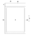
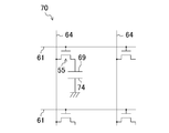
図18は、本発明の第3の実施形態に係る液晶表示装置の全体構成を示す平面図であり、図19は、本発明の第3の実施形態に係る液晶表示装置の断面図である。また、図20は、本発明の第3の実施形態に係る液晶表示装置の等価回路図であり、図21は、本発明の第3の実施形態に係る液晶表示装置を構成するTFT基板の全体構成を示す断面図である。また、図22は、本発明の第3の実施形態に係る液晶表示装置の表示部の全体構成を示す断面図である。なお、本実施形態においては、表示装置として、液晶表示装置を例に挙げて説明する。
図18は、本発明の第3の実施形態に係る液晶表示装置の全体構成を示す平面図であり、図19は、本発明の第3の実施形態に係る液晶表示装置の断面図である。また、図20は、本発明の第3の実施形態に係る液晶表示装置の等価回路図であり、図21は、本発明の第3の実施形態に係る液晶表示装置を構成するTFT基板の全体構成を示す断面図である。また、図22は、本発明の第3の実施形態に係る液晶表示装置の表示部の全体構成を示す断面図である。なお、本実施形態においては、表示装置として、液晶表示装置を例に挙げて説明する。
図18、図19に示す様に、液晶表示装置70は、第1基板であるTFT基板52と、TFT基板52に対向して配置された第2基板であるCF基板53とを備えている。また、液晶表示装置70は、TFT基板52及びCF基板53の間に挟持して設けられた表示媒体層である液晶層54と、TFT基板52とCF基板53との間に狭持され、TFT基板52及びCF基板53を互いに接着するとともに液晶層54を封入するために枠状に設けられたシール材80とを備えている。
このシール材80は、液晶層54を周回するように形成されており、TFT基板52とCF基板53は、このシール材80を介して相互に貼り合わされている。また、液晶表示装置70は、液晶層54の厚み(即ち、セルギャップ)を規制するための複数のフォトスペーサ(不図示)を備えている。
また、図18に示すように、液晶表示装置70は、矩形状に形成されており、液晶表示装置70の長手方向Aにおいて、TFT基板52がその上辺においてCF基板53よりも突出し、その突出した領域には、後述するゲート線やソース線等の複数の表示用配線が引き出され、端子領域Tが構成されている。
また、液晶表示装置70では、TFT基板52及びCF基板53が重なる領域に画像表示を行う表示領域Dが規定されている。ここで、表示領域Dは、画像の最小単位である画素がマトリクス状に複数配列されることにより構成される。
また、シール材80は、図18に示すように、表示領域Dの周囲全体を囲む矩形枠状に設けられている。このシール材80の枠幅は、特に限定されないが、例えば、0.5mm以上2.0mm以下に設定できる。
TFT基板52は、図20、図21に示すように、ガラス基板等の絶縁基板56と、当該絶縁基板56上に互いに平行に延設された複数のゲート線61と、各ゲート線61を覆うように設けられたゲート絶縁膜62とを備えている。また、TFT基板52は、ゲート絶縁膜62上に各ゲート線61と直交する方向に互いに平行に延設された複数のソース線64と、各ゲート線61及び各ソース線64の交差部分毎にそれぞれ設けられた複数のTFT素子55とを備えている。更に、TFT基板52は、各ソース線64及び各TFT素子55を覆うように順に設けられた層間絶縁膜60である第1層間絶縁膜65及び第2層間絶縁膜66と、第2層間絶縁膜66上にマトリクス状に設けられ、各TFT素子55の各々に接続された複数の画素電極69と、各画素電極69を覆うように設けられた配向膜59とを有している。
また、TFT素子55は、図21に示すように、各ゲート線61が側方に突出したゲート電極67と、ゲート電極67を覆うように設けられたゲート絶縁膜62と、ゲート絶縁膜62上でゲート電極67に重なる位置において島状に設けられた半導体層63とを備えている。また、TFT素子55は、半導体層63上で互いに対峙するように設けられたソース電極68及びドレイン電極77とを備えている。ここで、ソース電極68は、各ソース線64が側方に突出した部分である。また、ドレイン電極77は、図21に示すように、第1層間絶縁膜65及び第2層間絶縁膜66に形成されたコンタクトホール84を介して画素電極69に接続されている。また、画素電極69は、図22に示すように、第2層間絶縁膜66上に設けられた透明電極81と、透明電極81上に積層され、透明電極81の表面上に設けられた反射電極82とにより構成されている。また、半導体層63は、図21に示すように、下層の真性アモルファスシリコン層63aと、その上層のリンがドープされたn+アモルファスシリコン層63bとを備え、ソース電極68及びドレイン電極77から露出する真性アモルファスシリコン層63aがチャネル領域を構成している。
また、液晶表示装置70の表示部では、図22に示すように、反射電極82により反射領域Rが規定されている。また、画素電極69の下層の第2層間絶縁膜66の表面は、図22に示すように、凹凸状に形成されており、第2層間絶縁膜66の表面に透明電極81を介して設けられた反射電極82の表面も凹凸状に形成されている。
なお、第1層間絶縁膜65を構成する材料としては、特に限定されず、例えば、酸化シリコン(SiO2)、窒化シリコン(SiNx(xは正数))等が挙げられる。また、第1層間絶縁膜65の厚みは、600nm以上1000nm以下が好ましい。これは、第1層間絶縁膜65の厚みが600nm未満の場合は、第1層間絶縁膜65を平坦化することが困難になるという不都合が生じる場合があるためであり、1000nmより大きい場合は、エッチングにより、コンタクトホール84を形成することが困難になるという不都合が生じる場合があるためである。
また、CF基板53は、図22に示すように、ガラス基板等の絶縁基板71と、絶縁基板71上に設けられたカラーフィルター72と、カラーフィルター72の反射領域Rを覆うように設けられた共通電極74と、共通電極74上に柱状に設けられたフォトスペーサ(不図示)と、共通電極74及びフォトスペーサを覆うように設けられた配向膜76とを有している。
なお、カラーフィルター72には、図22に示すように、各画素に対して設けられた複数種の着色層78(即ち、赤色層R、緑色層G、および青色層B)と、遮光膜であるブラックマトリクス83とが含まれる。ブラックマトリクス83は、隣接する着色層78の間に設けられ、これら複数種の着色層78を区画する役割を有するものである。
このブラックマトリクス83は、Ta(タンタル)、Cr(クロム)、Mo(モリブデン)、Ni(ニッケル)、Ti(チタン)、Cu(銅)、Al(アルミニウム)などの金属材料、カーボンなどの黒色顔料が分散された樹脂材料、または、各々、光透過性を有する複数色の着色層が積層された樹脂材料などにより形成される。また、フォトスペーサは、例えば、アクリル系の感光性樹脂からなり、フォトリソグラフィー法により形成される。
そして、本実施形態においては、画素電極69と、画素電極状に形成された液晶層54と、液晶層54上に形成された共通電極74とにより、液晶表示素子85が構成されている。
上記構成の反射型の液晶表示装置70は、反射領域RにおいてCF基板53側から入射する光を反射電極82で反射するように構成されている。
そして、液晶表示装置70は、各画素電極69毎に1つの画素が構成されており、各画素において、ゲート線61からゲート信号が送られてTFT素子55をオン状態にした場合に、ソース線64からソース信号が送られてソース電極68及びドレイン電極77を介して、画素電極69に所定の電荷が書き込まれる。そして、画素電極69と共通電極74との間で電位差が生じ、液晶層54に所定の電圧が印加されるように構成されている。そして、液晶表示装置70では、印加された電圧の大きさに応じて、液晶分子の配向状態が変わることを利用して、CF基板53側から入射する光の反射率を調整することにより、画像が表示される構成となっている。
ここで、本実施形態の液晶表示装置70においても、上述の第1の実施形態の場合と同様に、図21、図22に示すように、絶縁基板56における液晶表示素子85側とは反対側の表面56b上にハニカム状の構造体30を備える点に特徴がある。
より具体的には、絶縁基板56の、液晶表示素子85が設けられた表面56aと反対側の表面56b上に、液晶表示装置70の剛性を向上するハニカム状の構造体30を設けている点に特徴がある。このハニカム状の構造体30は、上述の第1の実施形態の場合と同様に、絶縁基板56の表面56b上に接着剤層31を設け、接着剤層31を介して設ける構成としている。
このような構成により、上記(1)~(4)と同様の効果を得ることができる。即ち、液晶表示装置70の剛性を向上させることができるため、自重による撓みを防止することが可能になり、液晶表示装置70に反りやうねり等の変形が発生するのを防止することが可能になる。従って、液晶表示装置70の表示性能を向上させることができる。
また、自重による撓みを防止することができるため、液晶表示装置70の端部を把持した場合であっても、端部における支持に対して自立する(即ち、撓まず、変形しない)ため、液晶表示装置70の自立性を向上させることができる。
また、機械的なストレス等の外力により液晶表示装置70が屈曲した場合であっても、ハニカム状の構造体30のセル壁30aにより、応力40を分散することが可能になるため、液晶表示装置70の所定箇所における応力の集中を防止することが可能になる。従って、液晶表示装置70におけるクラック等の破損、金属配線の破断線、TFT素子55の破壊の発生を防止することが可能になるとともに、液晶表示装置70の歩留まりが低下を防止することが可能になる。
また、ユーザーが意図的に有機EL表示装置1に対して応力を加えた場合であっても、クラック等の破損、金属配線の破断線、TFT素子55の破壊を生じることなく、所望の形状に変形させることが可能になる。
また、以上に説明した本実施形態によれば、上記(5)~(7)と同様の効果を得ることができる。
なお、上記実施形態は以下のように変更しても良い。
上記実施形態においては、セル壁30aが断面略六角形状となるように配置され、セル壁30aにより区画された断面略六角形状を有するセル30bを備えるハニカム状の構造体30を挙げたが、上述の(1)~(4)の効果を奏するものであれば、セル壁30aの配置とセル30bの断面形状は、適宜変更することができる。
例えば、図23に示すように、セル壁43aが断面略円形状となるように配置されるとともに、セル壁43aにより区画された断面略円形状を有するセル43bを備えた構造体43を使用する構成としても良い。また、例えば、図24に示すように、セル壁47aが断面略三角形状となるように配置されるとともに、セル壁47aにより区画された断面略三角形状を有するセル47bを備えた構造体47を使用する構成としても良い。
また、図17に示すように、図2に示す有機EL表示装置1において、ハニカム状の構造体30をコート層45で被覆し、ハニカム状の構造体30とコート層45とからなるラミネート構造体46を有機基板2の表面2bにおいて、接着剤層31を介して、積層する構成としても良い。このような構成により、ハニカム状の構造体30が取り付けられた有機基板2の破損を効果的に防止することが可能になる。
また、同様に、図22に示す液晶表示装置70において、ハニカム状の構造体30をコート層45で被覆し、ハニカム状の構造体30とコート層45とからなるラミネート構造体46を絶縁基板56の表面56bにおいて、接着剤層31を介して、積層する構成としても良い。このような構成により、ハニカム状の構造体30が取り付けられた絶縁基板56の破損を効果的に防止することが可能になる。
コート層45を形成する材料としては、例えば、エポキシ樹脂を使用することができる。コート層45を形成する方法としては、例えば、ハニカム状の構造体30の表面において、エポキシ樹脂をCVD法によりコートする方法が採用できる。また、PET(ポリエチレンテレフタレート)やPEN(ポリエチレンナフタレート)により形成されたシート状のコート層45をハニカム状の構造体30の表面に貼り付けることによりラミネート構造体46を形成することもできる。また、コート層45の厚みとしては、例えば、300μmとすることができる。
なお、図14に示した構造体41や、図23、図24に示した構造体43,47をコート層45で被覆する構成としても、同様の効果を得ることができる。
また、上述の第3の実施形態において説明した液晶表示装置70において、ハニカム状の構造体30の代わりに、上述の第2の実施形態において説明した構造体41を使用する構成としても良い。この場合、構造体41のセル壁42は、液晶表示装置70の屈曲方向に延設された第1セル壁42aと、屈曲方向と直交する方向に延設された第2セル壁42bとから構成されることになる。このような構成により、上記(8)と同様の効果を得ることができる。
また、上記実施形態においては、TFT素子4として、アモルファスシリコンを用いたTFTを使用したが、TFT素子4として、酸化亜鉛系の半導体をチャネルとするTFT素子や有機半導体をチャネルとするTFT素子やカーボンナノチューブをチャネルとするTFT素子を使用する構成としても良い。この様な構成により、TFT素子4として、アモルファスシリコンを用いたTFTを使用する場合と同様に、汎用性のある材料により、大画面化が可能なTFT素子4を形成することが可能になる。
本実施形態においては、表示装置として有機EL(organic electro luminescence)、LCD(liquid crystal display;液晶表示ディスプレイ)に係るものについて示したが、表示装置は、電気泳動(electrophoretic)、PD(plasma display;プラズマディスプレイ)、PALC(plasma addressed liquid crystal display;プラズマアドレス液晶ディスプレイ)、無機EL(inorganic electro luminescence)、FED(field emission display;電界放出ディスプレイ)、又は、SED(surface-conduction electron-emitter display;表面電界ディスプレイ)等に係るものであってもよい。
以上説明したように、本発明は、フレキシブル性を有する有機EL表示装置等の表示装置について有用である。
1 有機EL表示装置
2 有機基板
2b 有機基板の表面
4 TFT素子
7 第1電極7
8 有機EL層
10 第2電極
11 有機EL表示素子
30 構造体
30a セル壁
30b セル
31 接着剤層
40 応力
41 構造体
42 セル壁
42a 第1セル壁
42b 第2セル壁
43 構造体
45 ラミネート層
47 構造体
54 液晶層
56 絶縁基板
56b 絶縁基板の表面
69 画素電極
70 液晶表示装置
74 共通電極
85 液晶表示素子
X 構造体の厚み方向
Y 屈曲方向
Z 屈曲方向と直交する方向
2 有機基板
2b 有機基板の表面
4 TFT素子
7 第1電極7
8 有機EL層
10 第2電極
11 有機EL表示素子
30 構造体
30a セル壁
30b セル
31 接着剤層
40 応力
41 構造体
42 セル壁
42a 第1セル壁
42b 第2セル壁
43 構造体
45 ラミネート層
47 構造体
54 液晶層
56 絶縁基板
56b 絶縁基板の表面
69 画素電極
70 液晶表示装置
74 共通電極
85 液晶表示素子
X 構造体の厚み方向
Y 屈曲方向
Z 屈曲方向と直交する方向
Claims (8)
- 基板と、前記基板上に形成された表示素子とを備える表示装置であって、
前記基板における前記表示素子側とは反対側に、セル壁によって区画された複数のセルを有する構造体が設けられていることを特徴とする表示装置。 - 前記セル壁が、樹脂材料または金属材料により形成されていることを特徴とする請求項1に記載の表示装置。
- 前記基板の表面上に接着剤層が設けられ、前記構造体が、接着剤層を介して設けられていることを特徴とする請求項1または請求項2に記載の表示装置。
- 前記構造体の厚みが、10μm~1mmであることを特徴とする請求項1~請求項3のいずれか1項に記載の表示装置。
- 前記構造体が、コート層により被覆されていることを特徴とする請求項1~請求項4のいずれか1項に記載の表示装置。
- 前記セル壁が、前記表示装置の屈曲方向に延設された第1セル壁と、前記屈曲方向と直交する方向に延設された第2セル壁とから構成されることを特徴とする請求項1~請求項5のいずれか1項に記載の表示装置。
- 前記表示素子が、有機EL表示素子であることを特徴とする請求項1~請求項6のいずれか1項に記載の表示装置。
- 前記表示素子が、液晶表示素子であることを特徴とする請求項1~請求項6のいずれか1項に記載の表示装置。
Priority Applications (1)
| Application Number | Priority Date | Filing Date | Title |
|---|---|---|---|
| US13/518,265 US20120262660A1 (en) | 2010-04-09 | 2011-03-28 | Display device |
Applications Claiming Priority (2)
| Application Number | Priority Date | Filing Date | Title |
|---|---|---|---|
| JP2010090670 | 2010-04-09 | ||
| JP2010-090670 | 2010-04-09 |
Publications (1)
| Publication Number | Publication Date |
|---|---|
| WO2011125307A1 true WO2011125307A1 (ja) | 2011-10-13 |
Family
ID=44762278
Family Applications (1)
| Application Number | Title | Priority Date | Filing Date |
|---|---|---|---|
| PCT/JP2011/001833 Ceased WO2011125307A1 (ja) | 2010-04-09 | 2011-03-28 | 表示装置 |
Country Status (2)
| Country | Link |
|---|---|
| US (1) | US20120262660A1 (ja) |
| WO (1) | WO2011125307A1 (ja) |
Cited By (8)
| Publication number | Priority date | Publication date | Assignee | Title |
|---|---|---|---|---|
| EP2599618A1 (en) * | 2011-11-30 | 2013-06-05 | Samsung Display Co., Ltd. | Cushion sheet and display device having the same |
| US20130313541A1 (en) * | 2011-03-30 | 2013-11-28 | Ocean's King Lighting Science & Technology Co., Ltd. | Substrate, manufacturing method thereof, and organo-electroluminescent device using the same |
| JP2013250551A (ja) * | 2012-05-01 | 2013-12-12 | Sumitomo Bakelite Co Ltd | 表示素子作製方法 |
| CN103544886A (zh) * | 2012-07-13 | 2014-01-29 | Lg电子株式会社 | 使用夹心蜂窝板的显示装置 |
| EP2712002A3 (en) * | 2012-09-19 | 2016-11-16 | Samsung Display Co., Ltd. | Organic light emitting diode display |
| JP2019053746A (ja) * | 2013-12-02 | 2019-04-04 | 株式会社半導体エネルギー研究所 | 電子機器 |
| CN110767664A (zh) * | 2019-10-31 | 2020-02-07 | 京东方科技集团股份有限公司 | 一种显示基板及其制作方法、显示装置 |
| US10806041B2 (en) | 2017-01-13 | 2020-10-13 | Daktronics, Inc. | Mounting structures for a banner display |
Families Citing this family (19)
| Publication number | Priority date | Publication date | Assignee | Title |
|---|---|---|---|---|
| KR101879831B1 (ko) * | 2012-03-21 | 2018-07-20 | 삼성디스플레이 주식회사 | 플렉시블 표시 장치, 유기 발광 표시 장치 및 플렉시블 표시 장치용 원장 기판 |
| JP5674707B2 (ja) * | 2012-05-22 | 2015-02-25 | 株式会社東芝 | 表示装置 |
| JP5955098B2 (ja) * | 2012-05-24 | 2016-07-20 | シャープ株式会社 | 液晶表示装置、データ線駆動回路、および液晶表示装置の駆動方法 |
| KR102068565B1 (ko) * | 2013-05-31 | 2020-01-21 | 엘지전자 주식회사 | 샌드위치 허니컴 패널을 이용한 디스플레이 장치 |
| US9203050B2 (en) | 2013-05-21 | 2015-12-01 | Samsung Display Co., Ltd. | Organic light emitting diode display and method of manufacturing the same |
| US11145838B2 (en) | 2013-05-21 | 2021-10-12 | Samsung Display Co., Ltd. | Organic light emitting diode display and method of manufacturing the same |
| JP6182985B2 (ja) * | 2013-06-05 | 2017-08-23 | セイコーエプソン株式会社 | 電気光学装置、電気光学装置の製造方法、電子機器 |
| KR102053244B1 (ko) | 2013-07-17 | 2019-12-09 | 삼성디스플레이 주식회사 | 윈도우 부재 및 그것을 포함하는 영상 표시 장치 |
| KR102092707B1 (ko) * | 2013-09-17 | 2020-03-25 | 삼성디스플레이 주식회사 | 플렉서블 디스플레이 장치와, 이의 제조 방법 |
| KR102132697B1 (ko) | 2013-12-05 | 2020-07-10 | 엘지디스플레이 주식회사 | 휘어진 디스플레이 장치 |
| JP6305050B2 (ja) * | 2013-12-18 | 2018-04-04 | キヤノン株式会社 | 画像処理装置、画像処理方法及びプログラム |
| KR102146844B1 (ko) * | 2013-12-23 | 2020-08-24 | 엘지디스플레이 주식회사 | 백라이트 유닛 및 이를 이용한 디스플레이 장치 |
| JP6659094B2 (ja) * | 2014-08-11 | 2020-03-04 | キヤノン株式会社 | 発光装置 |
| KR20160025152A (ko) * | 2014-08-26 | 2016-03-08 | 삼성디스플레이 주식회사 | 보호 구조물 및 보호 구조물을 포함하는 유기 발광 표시 장치 |
| TWI564650B (zh) * | 2015-01-30 | 2017-01-01 | Wi A股份有限公司 | 雷射反射型遮罩製造方法 |
| CN104600208B (zh) | 2015-02-05 | 2017-05-10 | 京东方科技集团股份有限公司 | 一种盖板、oled显示面板和显示装置 |
| CN108963075B (zh) * | 2018-07-23 | 2022-03-22 | 广州国显科技有限公司 | 支撑膜及其制备方法、显示模组、显示面板 |
| KR20220077715A (ko) * | 2020-12-02 | 2022-06-09 | 엘지디스플레이 주식회사 | 표시 장치 |
| KR102914208B1 (ko) | 2021-01-29 | 2026-01-21 | 삼성디스플레이 주식회사 | 표시 장치 |
Citations (8)
| Publication number | Priority date | Publication date | Assignee | Title |
|---|---|---|---|---|
| JPS5092751A (ja) * | 1973-12-15 | 1975-07-24 | ||
| JPH10189237A (ja) * | 1996-12-25 | 1998-07-21 | Casio Comput Co Ltd | 面発光体およびそれを使用する液晶表示装置 |
| JP2001305312A (ja) * | 2000-03-31 | 2001-10-31 | Three M Innovative Properties Co | 光学積層体 |
| JP2002278466A (ja) * | 2001-03-15 | 2002-09-27 | Minolta Co Ltd | 表示装置 |
| JP2003015545A (ja) * | 2001-07-02 | 2003-01-17 | Pioneer Electronic Corp | 画像表示パネル |
| WO2006090434A1 (ja) * | 2005-02-22 | 2006-08-31 | Fujifilm Corporation | 塑性変形を抑制する可撓性基材及び可撓性画像表示装置 |
| WO2007144995A1 (ja) * | 2006-06-15 | 2007-12-21 | Sharp Kabushiki Kaisha | 表示装置及びその製造方法 |
| WO2009038310A1 (en) * | 2007-09-21 | 2009-03-26 | Korea Advanced Institute Of Science And Technology | Polymer substrate for flexible display having enhanced flexibility |
Family Cites Families (5)
| Publication number | Priority date | Publication date | Assignee | Title |
|---|---|---|---|---|
| JP4522604B2 (ja) * | 2001-03-19 | 2010-08-11 | 日東電工株式会社 | 異方導電性フィルム |
| JP4052631B2 (ja) * | 2002-05-17 | 2008-02-27 | 株式会社東芝 | アクティブマトリクス型表示装置 |
| EP1970952A3 (en) * | 2007-03-13 | 2009-05-06 | Semiconductor Energy Laboratory Co., Ltd. | Semiconductor device and manufacturing method thereof |
| WO2009142310A1 (en) * | 2008-05-23 | 2009-11-26 | Semiconductor Energy Laboratory Co., Ltd. | Semiconductor device and method for manufacturing the same |
| JP5545970B2 (ja) * | 2009-03-26 | 2014-07-09 | 株式会社半導体エネルギー研究所 | 発光装置及びその作製方法 |
-
2011
- 2011-03-28 WO PCT/JP2011/001833 patent/WO2011125307A1/ja not_active Ceased
- 2011-03-28 US US13/518,265 patent/US20120262660A1/en not_active Abandoned
Patent Citations (8)
| Publication number | Priority date | Publication date | Assignee | Title |
|---|---|---|---|---|
| JPS5092751A (ja) * | 1973-12-15 | 1975-07-24 | ||
| JPH10189237A (ja) * | 1996-12-25 | 1998-07-21 | Casio Comput Co Ltd | 面発光体およびそれを使用する液晶表示装置 |
| JP2001305312A (ja) * | 2000-03-31 | 2001-10-31 | Three M Innovative Properties Co | 光学積層体 |
| JP2002278466A (ja) * | 2001-03-15 | 2002-09-27 | Minolta Co Ltd | 表示装置 |
| JP2003015545A (ja) * | 2001-07-02 | 2003-01-17 | Pioneer Electronic Corp | 画像表示パネル |
| WO2006090434A1 (ja) * | 2005-02-22 | 2006-08-31 | Fujifilm Corporation | 塑性変形を抑制する可撓性基材及び可撓性画像表示装置 |
| WO2007144995A1 (ja) * | 2006-06-15 | 2007-12-21 | Sharp Kabushiki Kaisha | 表示装置及びその製造方法 |
| WO2009038310A1 (en) * | 2007-09-21 | 2009-03-26 | Korea Advanced Institute Of Science And Technology | Polymer substrate for flexible display having enhanced flexibility |
Cited By (16)
| Publication number | Priority date | Publication date | Assignee | Title |
|---|---|---|---|---|
| US20130313541A1 (en) * | 2011-03-30 | 2013-11-28 | Ocean's King Lighting Science & Technology Co., Ltd. | Substrate, manufacturing method thereof, and organo-electroluminescent device using the same |
| US9059416B2 (en) * | 2011-03-30 | 2015-06-16 | Ocean's King Lighting Science & Technology Co., Ltd. | Substrate, manufacturing method thereof, and organo-electroluminescent device using the same |
| EP2599618A1 (en) * | 2011-11-30 | 2013-06-05 | Samsung Display Co., Ltd. | Cushion sheet and display device having the same |
| CN103137022A (zh) * | 2011-11-30 | 2013-06-05 | 三星显示有限公司 | 缓冲板及具有该缓冲板的显示设备 |
| US10076890B2 (en) | 2011-11-30 | 2018-09-18 | Samsung Display Co., Ltd. | Cushion sheet and display device having the same |
| CN103137022B (zh) * | 2011-11-30 | 2017-05-17 | 三星显示有限公司 | 缓冲板及具有该缓冲板的显示设备 |
| US9274360B2 (en) | 2011-11-30 | 2016-03-01 | Samsung Display Co., Ltd. | Cushion sheet and display device having the same |
| JP2013250551A (ja) * | 2012-05-01 | 2013-12-12 | Sumitomo Bakelite Co Ltd | 表示素子作製方法 |
| US9301411B2 (en) | 2012-07-13 | 2016-03-29 | Lg Electronics Inc. | Display device using sandwich honeycomb panel |
| EP2685444A3 (en) * | 2012-07-13 | 2014-09-17 | LG Electronics, Inc. | Display device using sandwich honeycomb panel |
| CN103544886A (zh) * | 2012-07-13 | 2014-01-29 | Lg电子株式会社 | 使用夹心蜂窝板的显示装置 |
| EP2712002A3 (en) * | 2012-09-19 | 2016-11-16 | Samsung Display Co., Ltd. | Organic light emitting diode display |
| JP2019053746A (ja) * | 2013-12-02 | 2019-04-04 | 株式会社半導体エネルギー研究所 | 電子機器 |
| US12229358B2 (en) | 2013-12-02 | 2025-02-18 | Semiconductor Energy Laboratory Co., Ltd. | Touch panel and method for manufacturing touch panel |
| US10806041B2 (en) | 2017-01-13 | 2020-10-13 | Daktronics, Inc. | Mounting structures for a banner display |
| CN110767664A (zh) * | 2019-10-31 | 2020-02-07 | 京东方科技集团股份有限公司 | 一种显示基板及其制作方法、显示装置 |
Also Published As
| Publication number | Publication date |
|---|---|
| US20120262660A1 (en) | 2012-10-18 |
Similar Documents
| Publication | Publication Date | Title |
|---|---|---|
| WO2011125307A1 (ja) | 表示装置 | |
| US10707429B2 (en) | Flexible display panel and flexible display apparatus | |
| JP7075916B2 (ja) | カバープレートおよびこれを含む折り畳み可能な表示装置 | |
| US10824256B2 (en) | Flexible display and method of manufacturing the same | |
| CN101911158B (zh) | 显示装置、液晶显示装置、有机el显示装置、薄膜基板以及显示装置的制造方法 | |
| CN110767086B (zh) | 可折叠显示装置及其背板 | |
| US9058074B2 (en) | Organic light emitting display | |
| US9196662B2 (en) | Organic light emitting display and method for manufacturing the same | |
| US10153322B2 (en) | Organic light emitting display device | |
| JP2004046115A (ja) | 表示装置及びその製造方法 | |
| JP6854268B2 (ja) | フレキシブル表示装置及びその製造方法 | |
| JP2006337983A (ja) | 可撓性表示装置の製造方法 | |
| US10268092B2 (en) | Display device | |
| CN101504947A (zh) | 半导体器件、电光装置、电子设备及其制造方法 | |
| JP2005099410A (ja) | フレキシブルマトリクス基板およびフレキシブル表示装置 | |
| JP2008070874A (ja) | 可撓性表示装置の製造装置及び製造方法 | |
| JP2018194600A (ja) | 表示装置 | |
| CN114582926A (zh) | 显示装置 | |
| KR101832270B1 (ko) | 액정표시소자 및 그 제조방법 | |
| KR102392989B1 (ko) | 플렉서블 표시장치 | |
| KR20070016772A (ko) | 가요성 표시 장치용 접착 테이프 및 이를 이용한 가요성표시 장치의 제조 방법 | |
| KR102631006B1 (ko) | 플렉서블 기판과 이를 포함하는 플렉서블 표시장치 및 그 제조 방법 | |
| KR102911310B1 (ko) | 유기 발광 표시 장치 | |
| WO2012049824A1 (ja) | 薄膜トランジスタ基板及びそれを用いた表示装置 | |
| JP2010262057A (ja) | 表示装置及びそれを備えた情報カード |
Legal Events
| Date | Code | Title | Description |
|---|---|---|---|
| 121 | Ep: the epo has been informed by wipo that ep was designated in this application |
Ref document number: 11765209 Country of ref document: EP Kind code of ref document: A1 |
|
| WWE | Wipo information: entry into national phase |
Ref document number: 13518265 Country of ref document: US |
|
| NENP | Non-entry into the national phase |
Ref country code: DE |
|
| 122 | Ep: pct application non-entry in european phase |
Ref document number: 11765209 Country of ref document: EP Kind code of ref document: A1 |
|
| NENP | Non-entry into the national phase |
Ref country code: JP |