WO2011122623A1 - 焼成用転写型フィルム及び焼成体を備えるガラス板の製造方法 - Google Patents
焼成用転写型フィルム及び焼成体を備えるガラス板の製造方法 Download PDFInfo
- Publication number
- WO2011122623A1 WO2011122623A1 PCT/JP2011/057811 JP2011057811W WO2011122623A1 WO 2011122623 A1 WO2011122623 A1 WO 2011122623A1 JP 2011057811 W JP2011057811 W JP 2011057811W WO 2011122623 A1 WO2011122623 A1 WO 2011122623A1
- Authority
- WO
- WIPO (PCT)
- Prior art keywords
- layer
- black
- conductive layer
- conductive
- film
- Prior art date
- Legal status (The legal status is an assumption and is not a legal conclusion. Google has not performed a legal analysis and makes no representation as to the accuracy of the status listed.)
- Ceased
Links
Images

Classifications
-
- H—ELECTRICITY
- H01—ELECTRIC ELEMENTS
- H01Q—ANTENNAS, i.e. RADIO AERIALS
- H01Q1/00—Details of, or arrangements associated with, antennas
- H01Q1/12—Supports; Mounting means
- H01Q1/1271—Supports; Mounting means for mounting on windscreens
Definitions
- the present invention relates to a transfer film for forming a decorative pattern such as a conductive pattern or pattern such as a wiring circuit or an electrode on a substrate such as glass, and in particular, a sintered body of an antenna pattern is formed on a vehicle-mounted window glass. It is related with the transfer film for baking suitable for doing.
- a conductive pattern such as an electric circuit on a substrate, forming an electrode pattern in a plasma display panel, forming an antenna on an in-vehicle glass plate, etc., and applying a conductive layer to a substrate such as glass by baking, It is done in each field.
- a conductive paste containing a conductive material such as silver and glass frit is used, and screen printing is performed on the substrate such as a glass plate.
- a method is used in which a conductive layer is directly formed by the printing method and then fired.
- Patent Document 1 discloses a method of forming an electric circuit pattern on glass, a printing pattern made of glass paste is formed on a transfer film, and the printing pattern is formed on a substrate.
- a transfer-type print pattern forming method is described in which the print pattern thermally transferred onto the substrate is baked.
- the method described in Patent Document 1 is a method in which an electric circuit is formed by screen printing on a transfer paper having an easily peelable layer formed on the surface, and this electric circuit is thermally transferred onto a substrate such as glass.
- a print pattern having a required area can be separately formed regardless of the area of the substrate, and a large-scale drying facility or a high-precision positioning device is not required. It is expected that the cost can be lowered.
- Patent Document 2 discloses that a conductive paste containing silver and a glass component is printed on the surface of a glass plate and includes at least one of copper oxide and chromium oxide thereon. A window glass with a sintered body in which a pigment paste is laminated is described.
- Patent Document 3 discloses a conductive paste containing a crystallized glass powder containing coloring components such as chromium oxide, cobalt oxide, copper oxide, a conductive substance powder such as silver, a low-melting glass, and an organic varnish. And a glass plate with a conductor, in which a conductor is formed by printing and baking the conductive paste on a glass plate.
- coloring components such as chromium oxide, cobalt oxide, copper oxide, a conductive substance powder such as silver, a low-melting glass, and an organic varnish.
- a glass plate with a conductor in which a conductor is formed by printing and baking the conductive paste on a glass plate.
- the glass frit for the conductive material is not suitable. It is necessary to increase the ratio, and it is necessary to increase the line width or to increase the film thickness in order to reduce the resistance value of the conductive layer, which makes it difficult to balance the conductive performance and the appearance. Further, as in the technique described in Patent Document 2 or Patent Document 3, a method of printing a pigment paste on a conductive paste or a method of using a conductive paste containing a coloring component, printing accuracy, conductive performance, appearance It is thought that the balance cannot be taken sufficiently.
- the present invention aims to solve these problems of the prior art, and provides a transfer film for firing having excellent electrical conductivity, chemical resistance, good appearance, and excellent transferability. is there.
- the present invention is a transfer-type film for baking comprising a transfer layer provided on a film substrate having peelability, wherein the transfer layer is a conductive layer containing at least a conductive material and a black containing at least a black pigment.
- the conductive layer with a black layer is formed by covering the surface of the conductive layer on the film base side having peelability with the black layer.
- the conductive layer with a black layer is formed by covering the surface of the conductive layer opposite to the film substrate having peelability with the black layer.
- the conductive layer with black layer is formed by laminating two black layers so as to sandwich the conductive layer.
- the conductive layer may have a conductive pattern including a power feeding portion, and the conductive layer with a black layer may be formed on a portion other than the power feeding portion of the conductive layer.
- the conductive layer may have an elongated conductive pattern, and the width of the black layer pattern may be wider than the width of the conductive pattern of the conductive layer.
- the transfer layer further includes a resin layer containing an organic substance that can be removed by baking, laminated on at least one of the peelable film base-side surface and the opposite surface of the conductive layer with a black layer. It is good also as what has.
- the appearance can be improved, the visibility can be improved, and the resin layer made of an organic material that can be removed by baking above and below the conductive layer with the black layer. If the layers are laminated, the transferability can be further improved.
- the transfer type film for baking of the present invention is provided with a black layer by peeling a film substrate, attaching a transfer layer having a conductive layer with a black layer to a glass plate, and simultaneously baking the conductive layer and the black layer.
- a glass plate provided with a fired body of a conductive layer can be produced, and in particular, it can be suitably used as an in-vehicle window glass provided with a fired body of a conductive layer with a black layer.
- the transfer film for baking of the present invention is excellent in transferability and can form a fired body excellent in visibility and chemical resistance on a substrate such as glass while ensuring conductivity.
- FIG. 1 is an enlarged cross-sectional model view illustrating the structure of a transfer film for baking according to the first embodiment of the present invention.
- a transfer layer 3 including a conductive layer 2 with a black layer is laminated on a film substrate 1 having peelability.
- a resin layer made of an organic material that can be removed by baking is laminated in order to improve transferability.
- a protective layer 4, a black layer 5, a conductive layer 6, an intermediate layer 7, and an adhesive layer 8 are laminated in this order on a peelable film substrate 1. It becomes the composition.
- a coating solution for the intermediate layer 7 is applied on the temporary support to form the intermediate layer 7, and a paste for the conductive layer 6 is formed thereon.
- the conductive layer 6 is formed by screen printing using a pattern plate, and then the paste for the black layer 5 is printed using the pattern by screen printing so as to cover the conductive layer 6.
- a black layer 5 is formed, and further a coating liquid for the protective layer 4 is applied thereon to form the protective layer 4, and a film substrate 1 having peelability is bonded to the first layer, and the first lamination is performed.
- a pressure-sensitive adhesive for the pressure-sensitive adhesive layer 8 is applied to another temporary support to form the pressure-sensitive adhesive layer 8 to obtain a second laminate.
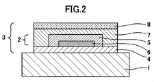
- FIG. 2 is an enlarged cross-sectional model view illustrating the structure of a transfer film for baking according to the second embodiment of the present invention.
- the relationship between the conductive layer 6 and the black layer 5 in the conductive layer with black layer 2 is upside down from the case of FIG.
- the intermediate layer 7 is formed on the temporary support.
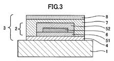
- FIG. 3 is an enlarged cross-sectional model view illustrating the structure of a transfer film for baking according to the third embodiment of the present invention.
- two black layers 51 and 52 are formed so as to sandwich the conductive layer 6.
- Such a laminated structure can be obtained by combining the methods as described above for the first embodiment and the second embodiment.
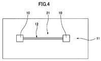
- FIG. 4 shows a pattern that can be used for forming the conductive layer 21 with the black layer by screen-printing the paste for the black layer 5 or the paste for the conductive layer 6 when manufacturing the transfer type film for baking of the present invention.
- the screen plate 11 includes a power supply unit 10 and a wiring unit 12.
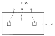
- FIG. 5 is a front view of the glass plate 9 provided with a fired body of the conductive layer 22 with a black layer produced using the transfer film for firing of the present invention.
- the film base material 1 having releasability used in the present invention may be any film as long as it has releasability from the transfer layer 3 including the conductive layer 2 with the black layer, and the film base material may be used as it is.
- the structure which formed the peeling layer which consists of a silicone type
- the film substrate 1 having releasability may be subjected to roughening treatment such as embossing or sandblasting for improving workability.
- a flexible substrate is preferable in consideration of the workability at the time of transfer.
- the thickness of the substrate is not particularly limited, and an optimum thickness may be selected from the viewpoint of the balance between pressure and heat transferability during transfer and the flexibility of the film, preferably 25 to 250 ⁇ m. A thickness of 35 to 125 ⁇ m, more preferably 50 to 75 ⁇ m, is preferably used for manufacturing or construction.
- the peelable film substrate 1 used in the present invention also has a role of a support when forming each layer of the transfer layer 3 including the conductive layer 2 with a black layer by a printing method or the like. Moreover, let the film base material 1 which has peelability shown in FIG.
- the film base material 1 which has 1st peelability, and another 2nd on the adhesion layer 8 surface of the transfer layer 3 containing the conductive layer 2 with a black layer.
- a peelable film substrate 1 ′ (not shown) was bonded together, and a transfer layer 3 including a black layered conductive layer 2 was sandwiched between the two peelable film substrates 1 and 1 ′. It is good also as a structure. In this case, at the peeling interface between the film substrate 1 ′ having the second peelability and the transfer layer 3 rather than the peeling load at the peeling interface between the film substrate 1 having the first peelability and the transfer layer 3. It is necessary that the peel load is lighter.
- the peeling load at the peeling interface can be adjusted depending on the type of substrate and peeling layer, the film thickness, and the like.
- the conductive layer 6 used in the present invention includes a conductive material for developing conductivity after firing, a glass frit for thermally fusing with a substrate to express mechanical strength, and an organic binder that can be removed by firing. Containing.
- a conductive material for developing conductivity after firing, a glass frit for thermally fusing with a substrate to express mechanical strength, and an organic binder that can be removed by firing. Containing.
- the conductive material powder of Au, Ag, Cu or the like, or powder of an alloy containing these can be used, and a material corresponding to a desired function after firing may be appropriately selected and used. From the viewpoint of forming a sintered body of a conductive layer, it is desirable to select a material that is excellent in conductivity, can be fired in the atmosphere, and is inexpensive, such as Ag, Ag-Pd, Ag-Pt, etc.
- a conductive material mainly composed of Ag can be preferably used.
- the conductive layer 6 in the present invention includes glass frit for the purpose of supporting the black layer-containing conductive layer 2 on the substrate after firing and improving durability.
- a glass frit having a suitable composition can be appropriately selected and used in consideration of a balance such as a firing temperature and a heat shrinkage rate.
- the organic binder to be contained in the conductive layer 6 of the present invention is not particularly limited as long as it is a material that can be removed by firing. Examples of materials that can be easily removed by thermal decomposition by firing include resins such as acrylic, methylcellulose, nitrocellulose, ethylcellulose, vinyl acetate, polyvinyl butyral, polyvinyl acetal, polyvinyl alcohol, polyethylene oxide, and polyester, and these are used alone or Can be used as a mixture.
- the plasticizer can be appropriately selected and used from fatty acid esters and phosphate esters.
- the black layer 5 used for this invention contains a glass frit and the organic binder which can be removed by baking other than a black pigment.
- the black pigment can be one or more kinds of black pigments selected from the group consisting of chromium oxide, cobalt oxide and copper oxide to exhibit concealability after firing and to make the appearance black.
- the glass frit exhibits mechanical strength, chemical resistance against sulfuric acid, salt water, and the like, and can be heat-sealed with the substrate.
- the glass frit and the organic binder those similar to those used for the conductive layer 6 can be appropriately selected and used.
- the black layer 5 used in the present invention contains an inorganic pigment component composed of a black pigment and glass frit, and an organic binder.
- the mixing ratio (P / R ratio) between the inorganic pigment component and the organic binder is preferably selected to a ratio of 80/20 to 95/5 in consideration of the balance between calcination properties and flexibility.
- the ratio between the black pigment and the glass frit contained in the black layer 5 may be selected from the balance between concealability and chemical resistance, and is preferably 20/80. If there is more glass frit than 20/80, concealability (blackness) will decrease, and if there is more black pigment than 20/80, chemical resistance may deteriorate, but it is not limited to the above preferred range. .
- the conductive layer 2 with a black layer covers the surface of the conductive layer 6 on the film base 1 side having peelability with the black layer 5. Is formed.
- the black layer 5 contains, in addition to the black pigment, a glass frit and an organic binder that can be removed by firing in the same manner as the conductive layer 6, the transfer type film having such a layer structure.
- a fired body of the conductive layer 2 with black layer having desired characteristics can be formed.
- FIG. 1 the second embodiment of the present invention, as shown in FIG.
- the conductive layer 2 with a black layer has a black layer on the surface of the conductive layer 6 opposite to the film substrate 1 having peelability. It is formed by being covered with 5.
- the conductive layer 2 with a black layer has a first black layer 51 and a second black layer 52 so as to sandwich the conductive layer 6.
- the conductive layer 6 is covered with the two black layers 51 and 52 from above and below, the conductive performance and appearance can be improved more efficiently.
- this invention utilizes the technique of a transfer type film, it is possible to provide a plurality of black layers with high accuracy.
- the conductive layer 2 with a black layer may be formed on a portion other than the power feeding portion of the conductive layer 6.
- the line width of the black layer 5 is preferably wider than the line width of the conductive layer 6.
- the pattern width of the black layer 5 is 0.2 mm or more wider than the pattern width of the conductive layer 6.
- the transferability of the fired transfer film of the present invention can be further improved by laminating a resin layer made of an organic material that can be removed by firing on the upper and lower sides of the conductive layer 2 with a black layer.
- the resin layer include an adhesive layer 8 for bonding to a substrate such as glass, an intermediate layer 7 for preventing the adhesive layer 8 from penetrating into the conductive layer 6 and the black layer 5, and a conductive layer after transfer. 6 or a protective layer 4 for preventing mechanical breakage of the black layer 5 can be provided.
- the pressure-sensitive adhesive layer 8 used in the present invention is not particularly limited as long as it is an organic substance that can be baked and removed when it is bonded to a substrate. Agents can be used. Moreover, when constructing by heat lamination etc., you may use the organic substance which softens at the lamination temperature.
- the pressure-sensitive adhesive layer 8 may be formed on the entire surface of the film substrate 1 having peelability so as to cover the conductive layer 2 with black layer, or a pattern similar to that of the conductive layer 2 with black layer may be formed. Good.
- the adhesive layer 8 is preferably formed so as to have a film thickness of 1 to 20 ⁇ m, preferably 2 to 10 ⁇ m. If the thickness is less than 1 ⁇ m, the adhesive strength is insufficient and the transferability is lowered.
- the thickness is greater than 20 ⁇ m, the amount of pyrolysis gas increases, so that the conductive layer 2 with black layer is likely to be defective and likely to be defective in firing.
- the thickness of the pressure-sensitive adhesive layer 8 is preferably as thin as possible within the range where the pressure-sensitive adhesive force can be maintained.
- the intermediate layer 7 can be provided between the conductive layer 2 with a black layer and the adhesive layer 8.
- the intermediate layer 7 can play a role of preventing the penetration of the solvent or organic substance contained in the adhesive used for forming the adhesive layer 8 into the conductive layer 2 with the black layer.
- the material used for the intermediate layer 7 is not particularly limited as long as it is an organic substance that can be removed by firing, and can be selected from the same organic binders used for the conductive layer and the black layer.
- a polymer resin having a temperature of 0 ° C. or higher can be preferably used.
- the intermediate layer 7 may be formed on the entire surface of the peelable film substrate 1 so as to cover the conductive layer 2 with black layer, or the same pattern as the conductive layer 2 with black layer may be formed.
- the thickness of the intermediate layer 7 is preferably 0.5 ⁇ m or more, and preferably 1 ⁇ m or more in order to stabilize the barrier effect. If the intermediate layer is thick, the amount of pyrolysis gas generated is increased, so that it is considered that defects are likely to occur in the conductive layer with black layer, resulting in poor firing, but it is not limited to the above range. From the above viewpoint, the intermediate layer 7 is desirably 10 ⁇ m or less, more preferably 5 ⁇ m or less, and is preferably as thin as possible.
- the protective layer 4 can be provided for the purpose of preventing foreign matters from adhering to the black-layered conductive layer 2 that has been transferred to the substrate before firing or causing scratches.
- the conductive layer 2 with a black layer before firing has a high content of inorganic pigment components such as a conductive material, a black pigment, and glass frit, and often has a small content of organic binder, so the film quality before firing tends to be hard and brittle. It is in. For this reason, when the transfer film is bent, the black conductive layer 2 is likely to crack. For this reason, the protective layer 4 can also play a role of preventing the occurrence of cracks when the film is bent.
- the material used for the protective layer 4 is not particularly limited as long as it is an organic substance that can be removed by firing, and can be selected from the same organic substances used for the conductive layer and the black layer.
- the protective layer 4 may be formed on the entire surface of the film substrate 1 having peelability so as to cover the conductive layer 2 with black layer, or a pattern similar to the conductive layer 2 with black layer may be formed. Good.
- the thickness of the protective layer 4 is preferably 3 to 6 ⁇ m.
- the conductive layer 2 with the black layer can be configured to be sandwiched between the protective layer 4 and the intermediate layer 7, so that the flexibility is improved and the bonding to the substrate or the transfer is performed. Workability is improved. Moreover, even if the conductive layer 2 with a black layer is formed in a shape such as a fine line or a dot, the protective layer 4, the intermediate layer 7, and the adhesive layer 8 are covered so as to cover the entire surface of the film substrate 1 having peelability. By forming, the contact area with the substrate can be increased without depending on the pattern shape and size of the conductive layer 2 with black layer, and the adhesive force can be sufficiently maintained. Furthermore, since the present invention is a technique using a transfer type film, it is possible to transfer a plurality of conductive layers 2 with a black layer at a time, and there are advantages such as improved positional accuracy.
- a printing method such as screen printing or offset printing, or a coating method such as gravure coating can be used.
- a coating method such as gravure coating
- a printing method is preferably used.
- the coating method is also used suitably.
- a coating liquid (paste) formed by dispersing or dissolving an inorganic pigment or an organic substance contained in each layer in a solvent is prepared and used.
- Solvents such as water-based, alcohol-based, ketone-based, ester-based, ether-based, and hydrocarbon-based solvents are used alone or in consideration of the dispersibility of inorganic pigments, the solubility of organic substances, and the boiling point suitable for the printing process. They can be used as a mixture.
- additives such as an antifoaming agent and a thickening agent may be used to prevent bubbles and adjust viscosity during printing.
- the solvent and additive those which are volatilized when each layer of the transfer layer is formed on the film base having releasability, or which can be volatilized or decomposed by firing are used.
- the transfer type film for baking of the present invention is bonded to a substrate such as a glass plate, and then peels off the peelable film base 1 and baked on the substrate to decompose and remove the organic matter, thereby providing the conductive layer 2 with a black layer.
- a fired body can be formed.
- Example 1 (Preparation of black layer paste) A black layer paste was prepared by dispersing a composite pigment of chromium oxide and copper oxide, glass frit, and an organic binder with three rolls.
- the black layer to be provided on the conductive layer in a state after transferring the baked transfer type film to the substrate, the black OC layer, A black layer to be provided under the conductive layer is referred to as a black AC layer.
- a transfer film for baking was prepared by the following procedure.
- a conductive layer paste “H4170” (manufactured by Shoei Chemical Industry Co., Ltd.) containing glass frit, Ag powder and an organic binder was prepared as a conductive layer paste.
- the intermediate layer coating solution was applied to the entire surface of the temporary support having the peelability with a Mayer bar so as to have a thickness of 1.5 ⁇ m to form an intermediate layer.
- the conductive layer paste is screen-printed using a plate having the pattern shown in FIG. 4, and the size of the wiring portion 12 is 0.2 mm wide ⁇ 50 mm long, and the size of the power feeding portion 10 is 5 mm ⁇ 5 mm thick. Printing was performed to 10 ⁇ m to form a conductive layer.
- the black layer paste produced as described above is subjected to screen printing, and the size of the portion shown in FIG. 4 excluding the power feeding portion 10, that is, the wiring portion 12, is 0.4 mm wide ⁇ 50 mm long.
- the laminated structure formed in this way has a temporary support at the position of the adhesive layer 8 when viewed in a cross section in a direction perpendicular to the length direction of the wiring portion 12, in the figure.
- An intermediate layer 7 is first formed on the lower surface having peelability, then a conductive layer 6 is formed, a black OC layer 5 is formed so as to cover the conductive layer 6, and a protective layer 4 is further formed. It will be in the state.
- a PET film “SRL-0504” manufactured by Lintec Co., Ltd. coated with a slightly adhesive layer was prepared as a film substrate having peelability according to the present invention.
- the fine adhesive surface of this PET film was bonded to the protective layer formed on the temporary support as described above, and pressure was applied from above the temporary support using a rubber roller at a pressure of 0.5 kg / cm. 1 laminate was produced.
- the protective layer 4 what formed the protective layer 4, the black OC layer 5, the conductive layer 6, and the intermediate
- a PET film “A31” (manufactured by Teijin DuPont Films, film size 20 cm ⁇ 30 cm thickness 50 ⁇ m) provided with a silicone release layer was prepared as another temporary support.
- Acrylic adhesive “SK1309” (manufactured by Soken Chemical Industry Co., Ltd.) was applied to the entire surface of the other temporary support having peelability using a Mayer bar to a thickness of 5 ⁇ m. 2 laminates were prepared.
- the temporary support is removed from the first laminate, the intermediate layer of the first laminate is bonded to the adhesive layer of the second laminate, and the transfer for firing that can be used as the transfer mold film for firing of the present invention.
- a mold film was prepared. In this way, with reference to FIG. 1, one in which an adhesive layer 8 is further formed on the intermediate layer 7 is obtained. In this state, in order to prevent dust from adhering to the adhesive layer, the other temporary support is not peeled off from the second laminate, and is left as it is.
- substrate provided with fired body of conductive layer with a black layer was produced in the following procedures.
- a glass plate (size 10 cm ⁇ 10 cm) produced by the float process was prepared. From the transfer film for firing prepared as described above, the other temporary support left behind was peeled off to expose the adhesive layer, and the adhesive layer side of the transfer film for firing was bonded to a glass plate. What was bonded together was arrange
- the film base material which has peelability was peeled, and the glass plate in which the laminated body (transfer layer) containing the conductive layer with a black layer was transferred was produced.
- the glass plate on which the transfer layer including the conductive layer with the black layer was transferred was baked in a state of being arranged substantially horizontally using a baking furnace “P90” (manufactured by Denken Co., Ltd.). Firing is carried out in an air atmosphere at a heating rate of 20 ° C / min from room temperature to 600 ° C, maintained at that temperature for 30 minutes, then stopped and cooled to 100 ° C or less by allowing it to cool in the furnace. By doing. The cooled glass plate was taken out from the baking furnace, and the glass substrate which formed the sintered body of the conductive layer with a black layer was obtained.
- Example 2 First, as in Example 1, an intermediate layer was formed on the temporary support.
- a black layer paste is first screen-printed thereon, and the size of the wiring portion 12 having the pattern shown in FIG. 4 is 0.4 mm wide ⁇ 50 mm long, and the size of the power feeding portion 10 is 5.4 mm ⁇ 5.4 mm.
- the black AC layer was formed by printing to a thickness of 5 ⁇ m.
- a conductive layer paste is applied on the black AC layer by screen printing so that the size of the wiring portion 12 of the pattern shown in FIG. 4 is 0.2 mm wide ⁇ 50 mm long, and the size of the power feeding portion 10 is 5 mm ⁇ 5 mm.
- the laminated structure formed in this way has a temporary support at the position of the adhesive layer 8 in the cross section in the direction perpendicular to the length direction of the wiring portion 12, with reference to FIG. First, the intermediate layer 7 is formed on the lower surface having peelability, the black AC layer 5 is formed, the conductive layer 6 is formed so as to be covered with the black AC layer 5, and the protective layer 4 is further formed.
- Example 2 a PET film “SRL-0504” (manufactured by Lintec Co., Ltd.) coated with a slightly adhesive layer was prepared, and the slightly adhesive surface of this PET film was temporarily supported as described above.
- the first laminate was manufactured by bonding to the protective layer formed above. Further, the temporary support is peeled off from the first laminate, and the intermediate layer of the first laminate is bonded to the adhesive layer of the second laminate similar to that used in Example 1, and the firing of the present invention.
- a transfer type film for firing that can be used as a transfer type film was prepared. Then, the glass substrate in which the sintered body of the conductive layer with a black layer was formed by the same method as Example 1 was produced.
- Example 3 First, as in Example 1, an intermediate layer was formed on the temporary support. Next, in the same manner as in Example 2, the black layer paste was applied thereon by screen printing, the size of the wiring portion 12 having the pattern shown in FIG. 4 was 0.4 mm wide ⁇ 50 mm long, and the size of the power feeding portion 10 was 5.4 mm. A black AC layer was formed by printing so as to be ⁇ 5.4 mm and a thickness of 5 ⁇ m. Next, a conductive layer paste is screen-printed on the black AC layer, the size of the wiring portion of the pattern shown in FIG. 4 is 0.2 mm wide ⁇ 50 mm long, and the size of the power feeding portion 10 is 5 mm ⁇ 5 mm thick.
- a conductive layer was formed so as to be covered with a black AC layer.
- the black layer paste was further screen-printed on this conductive layer, and the size of the portion of the pattern shown in FIG.
- a black OC layer was formed so as to cover the conductive layer by printing to be mm ⁇ length 50 mm and thickness 5 ⁇ m.
- the above-mentioned coating solution for the protective layer is applied using a Mayer bar so as to have a thickness of 5 ⁇ m, and covers the entire surface of the temporary support having the peelability, A protective layer was formed.
- the laminated structure formed in this way has a temporary support at the position of the adhesive layer 8 as seen in a cross section in the direction perpendicular to the length direction of the wiring portion 12.
- the intermediate layer 7 is formed on the lower surface having peelability, then the black AC layer 52 is formed, and the conductive layer 6 is formed so as to be surrounded by the black AC layer 52.
- the black OC layer 51 is formed so as to cover, and the protective layer 4 is further formed.
- a PET film “SRL-0504” manufactured by Lintec Co., Ltd. coated with a slightly adhesive layer was prepared, and the slightly adhesive surface of this PET film was temporarily supported as described above.
- the first laminate was manufactured by bonding to the protective layer formed above. Further, the temporary support is peeled off from the first laminate, and the intermediate layer of the first laminate is bonded to the adhesive layer of the second laminate similar to that used in Example 1, and the firing of the present invention.
- a transfer type film for firing that can be used as a transfer type film was prepared. Then, the glass substrate in which the sintered body of the conductive layer with a black layer was formed by the same method as Example 1 was produced.
- Example 1 First, as in Example 1, an intermediate layer was formed on the temporary support. Next, the conductive layer paste is screen-printed thereon so that the size of the wiring portion 12 of the pattern shown in FIG. 4 is 0.2 mm wide ⁇ 50 mm long, the size of the power feeding portion 10 is 5 mm ⁇ 5 mm, and the thickness is 10 ⁇ m. Printed as follows. Next, the coating liquid for the protective layer was applied using a Mayer bar so as to have a thickness of 5 ⁇ m, and a protective layer was formed so as to cover the entire surface of the temporary support on the peelable side.
- Example 1 a PET film “SRL-0504” (manufactured by Lintec Co., Ltd.) coated with a slightly adhesive layer was prepared, and the slightly adhesive surface of this PET film was temporarily supported as described above.
- the first laminate was manufactured by bonding to the protective layer formed above. Further, the temporary support is peeled off from the first laminate, and the intermediate layer of the first laminate is bonded to the adhesive layer of the second laminate similar to that used in Example 1, for comparison.
- a transfer type film for baking was prepared. Then, the glass substrate which formed the sintered body of the conductive layer which has not provided the black layer by the method similar to Example 1 was produced.
- the glass substrate on which the fired body was formed was immersed in 0.1N-sulfuric acid at 80 ° C. for 2 hours, rinsed with pure water, allowed to cool for 1 hour, and then subjected to the same evaluation as in the adhesion test.
- the brightness of the fired body formed on the glass substrate was measured using a spectrophotometer (manufactured by Konica Minolta Holding Co., Ltd.). For the purpose of evaluating the improvement of the visibility of the fired body of the conductive layer by providing the black layer, the fired body side for Example 1, the glass substrate side for Example 2, the fired body side and the glass substrate for Example 3 were used.
- Comparative Example 1 was measured from the fired body side and the glass substrate side for comparison.
- the evaluation was made by measuring the L * value defined in the color display method of JIS Z8729-2004, and when it was measured from the glass substrate side, it was rated as x when it was 10 or more, and it was marked as ⁇ when it was less than 10. Further, when measured from the fired body side, the case of 50 or more was evaluated as x, and the case of less than 50 was evaluated as ⁇ .
- Table 1 shows the evaluation results for Examples 1 to 3 and Comparative Example 1.
- Example 2 First, as in Example 1, an intermediate layer was formed on the temporary support. Next, the black layer paste is screen-printed thereon so that the size of the wiring portion 12 having the pattern shown in FIG. 4 is 0.2 mm wide ⁇ 50 mm long, the size of the power feeding portion 10 is 5 mm ⁇ 5 mm, and the thickness is 5 ⁇ m. Was printed to form a black AC layer. Next, a conductive layer paste is applied on the black AC layer by screen printing so that the size of the wiring portion 12 having the pattern shown in FIG.
- the size of the power feeding portion 10 is 5 mm ⁇ 5 mm ( That is, in the same pattern as in the case of the black layer paste), printing was performed to a thickness of 10 ⁇ m to form a conductive layer. Further, a black layer paste is applied on the conductive layer by screen printing, and the portion of the pattern shown in FIG. 4 excluding the power feeding portion 10, that is, the portion of the wiring portion 12, is 0.2 mm wide ⁇ 50 mm long. The film was printed to a thickness of 5 ⁇ m, and a black OC layer was printed on the conductive layer.
- the coating solution for the protective layer is applied to a thickness of 5 ⁇ m, so as to cover the entire surface of the temporary support that has the peelability, A protective layer was formed.
- a PET film “SRL-0504” manufactured by Lintec Corporation coated with a slightly adhesive layer was prepared, and the slightly adhesive surface of this PET film was temporarily supported as described above.
- the first laminate was manufactured by bonding to the protective layer formed above. Further, the temporary support is peeled off from the first laminate, and the intermediate layer of the first laminate is bonded to the adhesive layer of the second laminate similar to that used in Example 1, for comparison.
- a transfer type film for baking was prepared.
- Example 2 the glass substrate in which the fired body of the conductive layer with a black layer was formed by the same method as Example 1 was produced.
- Evaluation For the glass substrate on which the fired body produced in Comparative Example 2 was formed, the following evaluation was performed in comparison with the glass substrate on which the fired body produced in Example 3 was formed.
- (Lamination test) When the conductive layer with a black layer formed on the glass substrate is observed with an optical magnifying glass (Eschenbach Optical Japan Co., Ltd., ⁇ 10) before firing, the conductive layer is in the black layer. The case where the conductive layer protruded from the black layer was evaluated as x.
- Acid resistance test The acid resistance was evaluated by the same method as in Examples 1 to 3 and Comparative Example 1. Table 2 shows the evaluation results for Example 3 and Comparative Example 2.
- Example 3 was good in both stackability and acid resistance, but Comparative Example 2 was poor in stackability and acid resistance.
- the transfer film for baking of the present invention it is possible to form a fired body excellent in visibility and chemical resistance on a substrate such as glass while ensuring excellent transferability and electrical conductivity.
- the transfer film for baking of this invention can be used suitably as a product for vehicle-mounted window glass, such as the case where an antenna is formed on the windshield of an automobile that places importance on good visibility.
Landscapes
- Decoration By Transfer Pictures (AREA)
- Laminated Bodies (AREA)
- Surface Treatment Of Glass (AREA)
Abstract
導電性能、耐薬品性に優れ、外観が良く、また、転写性に優れた焼成用転写フィルムを提供する。 剥離性を有するフィルム基材上に設けられた、少なくとも導電性材料を含む導電層と、少なくとも黒色顔料を含む黒色層とからなる、黒色層付導電層を有する転写層を備える、焼成用転写型フィルム。導電層及び黒色層はさらに、ガラスフリットと、焼成により除去可能な有機バインダーとを含み、黒色層付導電層は、導電層が黒色層で覆われるように、黒色層及び導電層を積層することにより形成されている。
Description
本発明は、ガラス等の基板に配線回路や電極等の導電性パターンや模様等の装飾パターンを形成するための転写フィルムに関するものであり、特に、車載用窓ガラスにアンテナパターンの焼成体を形成するのに適した、焼成用転写フィルムに関するものである。
従来、基板上への電気回路等の導電性パターンの形成、プラズマディスプレイパネルにおける電極パターンの形成、車載用ガラス板へのアンテナ形成など、ガラス等の基板に焼成により導電層を付与することが、各分野で行われている。
従来、ガラス板などの基板上への導電層の焼成体を形成する方法としては、銀などの導電性材料とガラスフリットを含有した導電性ペーストを用い、ガラス板などの基板上にスクリーン印刷などの印刷方法で導電層を直接形成した後、焼成する方法が一般に用いられている。
しかしながら、この方法では、大面積の基板上に小面積の印刷パターンを直接形成する場合や、印刷パターンの積層体を形成する場合に、基板の位置精度を高く確保しつつ位置決めする必要があり、大規模な乾燥設備や高精度の位置決め装置などが必要となって、コストが高くなるという問題があった。
従来、ガラス板などの基板上への導電層の焼成体を形成する方法としては、銀などの導電性材料とガラスフリットを含有した導電性ペーストを用い、ガラス板などの基板上にスクリーン印刷などの印刷方法で導電層を直接形成した後、焼成する方法が一般に用いられている。
しかしながら、この方法では、大面積の基板上に小面積の印刷パターンを直接形成する場合や、印刷パターンの積層体を形成する場合に、基板の位置精度を高く確保しつつ位置決めする必要があり、大規模な乾燥設備や高精度の位置決め装置などが必要となって、コストが高くなるという問題があった。
このような問題を解決する方法として、例えば、特許文献1には、電気回路パターンをガラスに形成する方法であって、転写フィルム上にガラスペーストよりなる印刷パターンを形成し、この印刷パターンを基板上に熱転写し、基板上に熱転写された印刷パターンを焼成する転写式印刷パターン形成方法が記載されている。
特許文献1に記載されている方法は、易剥離層が表面に形成された転写紙の上に電気回路をスクリーン印刷で形成し、この電気回路をガラス等の基板の上に熱転写する方法である。特許文献1に記載されている方法によれば、必要な面積の印刷パターンを基板の面積に関係なく別に形成することができ、大規模な乾燥設備や高精度の位置決め装置などが不要となって、コストを低くすることが可能となることが、期待される。
特許文献1に記載されている方法は、易剥離層が表面に形成された転写紙の上に電気回路をスクリーン印刷で形成し、この電気回路をガラス等の基板の上に熱転写する方法である。特許文献1に記載されている方法によれば、必要な面積の印刷パターンを基板の面積に関係なく別に形成することができ、大規模な乾燥設備や高精度の位置決め装置などが不要となって、コストを低くすることが可能となることが、期待される。
さらに最近では、ガラス板などの透明性の基板上に導電層を形成する場合、導電層の色をより暗色にしたいという要求がある。これは導電性ペーストに含まれる銀を主成分とした導電性材料を基板上で焼き付けると、銀コロイドの発色により導電層の色が黄変し、外見上見栄えが悪くなるためである。
このような問題を解決するための技術として、特許文献2には、銀およびガラス成分を含む導電性ペーストをガラス板の表面に印刷形成し、その上に酸化銅および酸化クロムの少なくとも一方を含む顔料ペーストを積層した、焼結体付窓ガラスが記載されている。
さらに、特許文献3には、酸化クロム、酸化コバルト、酸化銅などの着色成分を含有する結晶化ガラスの粉末、銀などの導電性物質の粉末、低融点ガラスおよび有機質ワニスを含有する導電性ペースト、及びこの導電性ペーストをガラス板に印刷・焼成して導電体を形成した、導電体付ガラス板が記載されている。
このような問題を解決するための技術として、特許文献2には、銀およびガラス成分を含む導電性ペーストをガラス板の表面に印刷形成し、その上に酸化銅および酸化クロムの少なくとも一方を含む顔料ペーストを積層した、焼結体付窓ガラスが記載されている。
さらに、特許文献3には、酸化クロム、酸化コバルト、酸化銅などの着色成分を含有する結晶化ガラスの粉末、銀などの導電性物質の粉末、低融点ガラスおよび有機質ワニスを含有する導電性ペースト、及びこの導電性ペーストをガラス板に印刷・焼成して導電体を形成した、導電体付ガラス板が記載されている。
しかしながら、特許文献1に記載されている方法により得られる焼成後の導電層について、耐久性などの要請から、硫酸や塩水等の薬品に対する耐性を持たせるためには、導電性材料に対するガラスフリットの比率を増やす必要があり、導電層の抵抗値を低くするため線幅を太くするもしくは厚膜化する必要が生ずるため、導電性能と外観のバランスを取るのが難しくなってしまう。
また、特許文献2あるいは特許文献3に記載されている技術のように、導電ペースト上に顔料ペースト印刷する方法や、着色成分を含有させた導電ペーストを用いる方法では、印刷精度や導電性能、外観とのバランスを、十分に取ることはできないと考えられる。
また、特許文献2あるいは特許文献3に記載されている技術のように、導電ペースト上に顔料ペースト印刷する方法や、着色成分を含有させた導電ペーストを用いる方法では、印刷精度や導電性能、外観とのバランスを、十分に取ることはできないと考えられる。
本発明は、これら従来技術の課題を解決することを目的とするものであり、導電性能、耐薬品性に優れ、外観が良く、また、転写性に優れた焼成用転写フィルムを提供するものである。
本発明は、剥離性を有するフィルム基材上に設けられた転写層を備える、焼成用転写型フィルムであって、転写層は、少なくとも導電性材料を含む導電層と、少なくとも黒色顔料を含む黒色層とからなる、黒色層付導電層を有し、導電層及び黒色層は、さらに、ガラスフリットと、焼成により除去可能な有機バインダーとを含み、黒色層付導電層は、導電層が黒色層で覆われるように、黒色層及び導電層を積層することにより形成されている、焼成用転写型フィルムである。
本発明の一実施形態によると、黒色層付導電層は、剥離性を有するフィルム基材側の導電層の面を黒色層によって覆うことにより、形成されている。
本発明の別の実施形態によると、黒色層付導電層は、剥離性を有するフィルム基材とは反対側の導電層の面が黒色層によって覆われるようにすることにより、形成されている。
本発明のさらに別の実施形態によると、黒色層付導電層は、導電層を挟むように2つの黒色層を積層することにより、形成されている。
本発明の別の実施形態によると、黒色層付導電層は、剥離性を有するフィルム基材とは反対側の導電層の面が黒色層によって覆われるようにすることにより、形成されている。
本発明のさらに別の実施形態によると、黒色層付導電層は、導電層を挟むように2つの黒色層を積層することにより、形成されている。
本発明において、導電層は、給電部を備える導電性パターンを有し、黒色層付導電層は、導電層の給電部以外の部分について形成されるようにしてもよい。
また、本発明において、導電層は、細長形状の導電性パターンを有し、黒色層のパターンの幅は、導電層の導電性パターンの幅よりも広くなるようにしてもよい。
さらに、本発明において、転写層はさらに、黒色層付導電層の剥離性を有するフィルム基材側の面及び反対側の面の少なくとも一方に積層された、焼成により除去可能な有機物を含む樹脂層を有するものとしてもよい。
また、本発明において、導電層は、細長形状の導電性パターンを有し、黒色層のパターンの幅は、導電層の導電性パターンの幅よりも広くなるようにしてもよい。
さらに、本発明において、転写層はさらに、黒色層付導電層の剥離性を有するフィルム基材側の面及び反対側の面の少なくとも一方に積層された、焼成により除去可能な有機物を含む樹脂層を有するものとしてもよい。
本発明によれば、導電層を黒色層で覆うことにより、外観を改善し、視認性を向上させることができ、さらに、黒色層付導電層の上下に焼成により除去可能な有機物よりなる樹脂層を積層すれば、転写性を一層向上させることができる。
本発明の焼成用転写型フィルムは、フィルム基材を剥離して、黒色層付導電層を有する転写層をガラス板に貼りつけ、導電層と黒色層とを同時に焼成することで、黒色層付導電層の焼成体を備えたガラス板の製造することができ、特に、黒色層付導電層の焼成体を備えた車載用窓ガラスとして、好適に用いることができる。
本発明の焼成用転写フィルムは、転写性に優れ、導電性を確保しつつ、視認性および耐薬品性に優れた焼成体をガラス等の基板上に形成することができるものである。
本発明の焼成用転写型フィルムは、フィルム基材を剥離して、黒色層付導電層を有する転写層をガラス板に貼りつけ、導電層と黒色層とを同時に焼成することで、黒色層付導電層の焼成体を備えたガラス板の製造することができ、特に、黒色層付導電層の焼成体を備えた車載用窓ガラスとして、好適に用いることができる。
本発明の焼成用転写フィルムは、転写性に優れ、導電性を確保しつつ、視認性および耐薬品性に優れた焼成体をガラス等の基板上に形成することができるものである。
以下に本発明について詳細に説明する。
図1は、本発明の第1の実施形態による焼成用転写型フィルムの構造を例示する拡大断面模型図である。
図1を参照して、剥離性を有するフィルム基材1の上には、黒色層付導電層2を含む転写層3が積層されている。黒色層付導電層2の上下には、転写性を向上させるために、焼成除去可能な有機物よりなる樹脂層が積層されている。具体的には、この実施形態による焼成用転写型フィルムは、剥離性を有するフィルム基材1上に保護層4、黒色層5、導電層6、中間層7、粘着層8がこの順に積層された構成となっている。
このような積層構造を形成するには、例えば、まず、中間層7用の塗布液を仮支持体の上に塗布して中間層7を形成し、その上に、導電層6用のペーストを、パターンの版を用いてスクリーン印刷により印刷して、導電層6を形成し、次に、黒色層5用のペーストを、スクリーン印刷によりパターンを用いて印刷して、導電層6を覆うように黒色層5を形成し、この上にさらに、保護層4用の塗布液を塗布して保護層4を形成し、そこに、剥離性を有するフィルム基材1を貼り合わせて、第1の積層物を得る。他方、別の仮支持体に、粘着層8用の粘着剤を塗布し、粘着層8を形成して、第2の積層物を得る。最後に、第1の積層物から仮支持体を剥がし、第1の積層物の中間層7を第2の積層物の粘着層8と貼り合わせれば、本発明の焼成用転写型フィルムを作製することができる。
図2は、本発明の第2の実施形態による焼成用転写型フィルムの構造を例示する拡大断面模型図である。図2では、黒色層付導電層中2の導電層6と黒色層5との関係が、図1の場合とは上下逆になっている。
このような積層構造を形成するには、例えば、まず第1の実施形態と同様に、仮支持体の上に中間層7を形成する。第2の実施形態では、その上に、まず黒色層5用のペーストを印刷して、黒色層5を形成し、この黒色層5の上に、導電層6用のペーストを印刷して、黒色層5によって覆われるように、導電層6を形成する。以下、第1の実施形態と同様に、保護層4を形成し、そこに剥離性を有するフィルム基材1を貼り合わせて第1の積層物を得る一方、別の仮支持体に粘着層8を形成して第2の積層物を得、第1の積層物から仮支持体を剥がし、第1の積層物の中間層7を第2の積層物の粘着層8と貼り合わせればよい。
図3は、本発明の第3の実施形態による焼成用転写型フィルムの構造を例示する拡大断面模型図である。図3では、導電層6を挟むように2つの黒色層51、52が形成されている。
このような積層構造は、第1の実施形態及び第2の実施形態について上記したような方法を組み合わせることにより、得ることができるものである。
図1は、本発明の第1の実施形態による焼成用転写型フィルムの構造を例示する拡大断面模型図である。
図1を参照して、剥離性を有するフィルム基材1の上には、黒色層付導電層2を含む転写層3が積層されている。黒色層付導電層2の上下には、転写性を向上させるために、焼成除去可能な有機物よりなる樹脂層が積層されている。具体的には、この実施形態による焼成用転写型フィルムは、剥離性を有するフィルム基材1上に保護層4、黒色層5、導電層6、中間層7、粘着層8がこの順に積層された構成となっている。
このような積層構造を形成するには、例えば、まず、中間層7用の塗布液を仮支持体の上に塗布して中間層7を形成し、その上に、導電層6用のペーストを、パターンの版を用いてスクリーン印刷により印刷して、導電層6を形成し、次に、黒色層5用のペーストを、スクリーン印刷によりパターンを用いて印刷して、導電層6を覆うように黒色層5を形成し、この上にさらに、保護層4用の塗布液を塗布して保護層4を形成し、そこに、剥離性を有するフィルム基材1を貼り合わせて、第1の積層物を得る。他方、別の仮支持体に、粘着層8用の粘着剤を塗布し、粘着層8を形成して、第2の積層物を得る。最後に、第1の積層物から仮支持体を剥がし、第1の積層物の中間層7を第2の積層物の粘着層8と貼り合わせれば、本発明の焼成用転写型フィルムを作製することができる。
図2は、本発明の第2の実施形態による焼成用転写型フィルムの構造を例示する拡大断面模型図である。図2では、黒色層付導電層中2の導電層6と黒色層5との関係が、図1の場合とは上下逆になっている。
このような積層構造を形成するには、例えば、まず第1の実施形態と同様に、仮支持体の上に中間層7を形成する。第2の実施形態では、その上に、まず黒色層5用のペーストを印刷して、黒色層5を形成し、この黒色層5の上に、導電層6用のペーストを印刷して、黒色層5によって覆われるように、導電層6を形成する。以下、第1の実施形態と同様に、保護層4を形成し、そこに剥離性を有するフィルム基材1を貼り合わせて第1の積層物を得る一方、別の仮支持体に粘着層8を形成して第2の積層物を得、第1の積層物から仮支持体を剥がし、第1の積層物の中間層7を第2の積層物の粘着層8と貼り合わせればよい。
図3は、本発明の第3の実施形態による焼成用転写型フィルムの構造を例示する拡大断面模型図である。図3では、導電層6を挟むように2つの黒色層51、52が形成されている。
このような積層構造は、第1の実施形態及び第2の実施形態について上記したような方法を組み合わせることにより、得ることができるものである。
図4は、本発明の焼成用転写型フィルムを製造する際、黒色層5用のペーストあるいは導電層6用のペーストをスクリーン印刷して黒色層付導電層21をするのに使用しうるパターンを備えるスクリーン版11であって、給電部10及び配線部12を備えるものである。
図5は、本発明の焼成用転写型フィルムを用いて製造した黒色層付導電層22の焼成体を備えたガラス板9の正面図である。
図5は、本発明の焼成用転写型フィルムを用いて製造した黒色層付導電層22の焼成体を備えたガラス板9の正面図である。
本発明に用いる剥離性を有するフィルム基材1は、黒色層付導電層2を含む転写層3と剥離性を有するものであれば良く、フィルム基材をそのまま用いても良いが、必要によりフィルム基材上にシリコーン系やアルキド樹脂系などからなる剥離層や再剥離用の微粘着層を形成した構成であっても良い。また剥離性を有するフィルム基材1は、施工性向上のために、エンボス加工やサンドブラスト等の粗面化処理したものであっても良い。
剥離性を有するフィルム基材1としては、転写時の施工性を考慮して、フレキシブル性のある基材が好ましく、例えば、ポリエチレン、ポリイミド、ポリエチレンテレフタレート、アクリルなどのプラスチックや紙などを使用できる。また、基材の厚みは特に限定されるものではなく、転写時の圧力や熱の伝達性とフィルムの屈曲性とのバランスの点から最適な厚みを選定すればよいが、25~250μm、好ましくは35~125μm、さらに好ましくは50~75μmの厚さが、製造上もしくは施工上好適に用いられる。
本発明に用いる剥離性を有するフィルム基材1は、黒色層付導電層2を含む転写層3の各層を印刷方式等で形成するときの支持体の役割も有している。また、図3に示す剥離性を有するフィルム基材1を第1の剥離性を有するフィルム基材1とし、黒色層付導電層2を含む転写層3の粘着層8面に別の第2の剥離性を有するフィルム基材1’(図示せず)を貼り合わせ、この2枚の剥離性を有するフィルム基材1,1’の間に黒色層付導電層2を含む転写層3を挟持した構成としてもよい。この場合、第1の剥離性を有するフィルム基材1と転写層3との剥離界面での剥離荷重よりも、第2の剥離性を有するフィルム基材1’と転写層3との剥離界面での剥離荷重の方が軽いことが必要である。剥離界面での剥離荷重は、基材や剥離層の種類、膜厚などによって調整可能である。
剥離性を有するフィルム基材1としては、転写時の施工性を考慮して、フレキシブル性のある基材が好ましく、例えば、ポリエチレン、ポリイミド、ポリエチレンテレフタレート、アクリルなどのプラスチックや紙などを使用できる。また、基材の厚みは特に限定されるものではなく、転写時の圧力や熱の伝達性とフィルムの屈曲性とのバランスの点から最適な厚みを選定すればよいが、25~250μm、好ましくは35~125μm、さらに好ましくは50~75μmの厚さが、製造上もしくは施工上好適に用いられる。
本発明に用いる剥離性を有するフィルム基材1は、黒色層付導電層2を含む転写層3の各層を印刷方式等で形成するときの支持体の役割も有している。また、図3に示す剥離性を有するフィルム基材1を第1の剥離性を有するフィルム基材1とし、黒色層付導電層2を含む転写層3の粘着層8面に別の第2の剥離性を有するフィルム基材1’(図示せず)を貼り合わせ、この2枚の剥離性を有するフィルム基材1,1’の間に黒色層付導電層2を含む転写層3を挟持した構成としてもよい。この場合、第1の剥離性を有するフィルム基材1と転写層3との剥離界面での剥離荷重よりも、第2の剥離性を有するフィルム基材1’と転写層3との剥離界面での剥離荷重の方が軽いことが必要である。剥離界面での剥離荷重は、基材や剥離層の種類、膜厚などによって調整可能である。
本発明に用いる導電層6は、焼成後の導電性を発現するための導電性材料と、基板と熱融着して機械的強度を発現するためガラスフリットと、焼成により除去可能な有機バインダーとを含有する。
導電性材料としては、Au、Ag、Cu等の粉体や、これらを含む合金の粉体を用いることができ、焼成後の所望の機能に応じた材料を適宜選択して使用すればよい。導電層の焼結体を形成するという観点から、導電性に優れると共に、大気中での焼成が可能で、且つ安価である材料を選択するのが望ましく、Ag、Ag-Pd、Ag-Pt等のAgを主成分とした導電性材料を好適に用いることができる。
本発明における導電層6は、黒色層付導電層2を焼成後に基板に担持させ、耐久性を向上させるなどの目的のために、ガラスフリットを含んでなる。ガラスフリットは、焼成温度や熱収縮率などのバランスを考慮して、好適な組成のものを適宜選定して用いることができる。
本発明の導電層6に含有せしめる有機物バインダーとしては、焼成除去可能な材料であれば特に限定されない。焼成による熱分解によって除去されやすい材料としては、アクリル、メチルセルロース、ニトロセルロース、エチルセルロース、酢酸ビニル、ポリビニルブチラール、ポリビニルアセタール、ポリビニルアルコール、ポリエチレンオキサイド、ポリエステルなどの樹脂が挙げられ、これらを単独で、または混合して使用することができる。また、有機成分として、焼成前の塗膜に可とう性を付与する目的で、可塑剤を加えてもよい。可塑剤は、脂肪酸エステルやリン酸エステルなどの中から、適宜選定して用いることができる。
導電性材料としては、Au、Ag、Cu等の粉体や、これらを含む合金の粉体を用いることができ、焼成後の所望の機能に応じた材料を適宜選択して使用すればよい。導電層の焼結体を形成するという観点から、導電性に優れると共に、大気中での焼成が可能で、且つ安価である材料を選択するのが望ましく、Ag、Ag-Pd、Ag-Pt等のAgを主成分とした導電性材料を好適に用いることができる。
本発明における導電層6は、黒色層付導電層2を焼成後に基板に担持させ、耐久性を向上させるなどの目的のために、ガラスフリットを含んでなる。ガラスフリットは、焼成温度や熱収縮率などのバランスを考慮して、好適な組成のものを適宜選定して用いることができる。
本発明の導電層6に含有せしめる有機物バインダーとしては、焼成除去可能な材料であれば特に限定されない。焼成による熱分解によって除去されやすい材料としては、アクリル、メチルセルロース、ニトロセルロース、エチルセルロース、酢酸ビニル、ポリビニルブチラール、ポリビニルアセタール、ポリビニルアルコール、ポリエチレンオキサイド、ポリエステルなどの樹脂が挙げられ、これらを単独で、または混合して使用することができる。また、有機成分として、焼成前の塗膜に可とう性を付与する目的で、可塑剤を加えてもよい。可塑剤は、脂肪酸エステルやリン酸エステルなどの中から、適宜選定して用いることができる。
本発明に用いる黒色層5は、黒色顔料のほか、ガラスフリットと、焼成により除去可能な有機バインダーとを含む。黒色顔料は、焼成後に隠蔽性を発現し、外観を黒色に見せるための酸化クロム、酸化コバルトおよび酸化銅からなる群から選ばれた1種類以上の黒色顔料とすることができる。ガラスフリットは、機械的強度、硫酸や塩水等に対する耐薬品性を発現し、基板と熱融着可能なものである。ガラスフリットおよび有機バインダーとしては、導電層6に用いるものと同様のものを、適宜選定して用いることができる。
本発明に用いる黒色層5は、黒色顔料及びガラスフリットからなる無機顔料成分と、有機バインダーとを含有する。このため無機顔料成分と有機バインダーとの混合比(P/R比)を、焼成性と屈曲性とのバランスを考慮して、80/20~95/5の比率に選定するのが好ましい。95/5より高くなると屈曲性が悪くなり断線、割れが発生し、80/20より低くなると焼成時の有機バインダーの熱分解ガスの発生量が多くなるため、焼成後の黒色層付導電層に空隙などの欠陥が生じやすく焼成不良になりやすいと考えられるが、上記好ましい範囲に限定されるものではない。
また、黒色層5に含まれる黒色顔料とガラスフリットとの比率は、隠蔽性と耐薬品性とのバランスから最適な比率を選定すれば良く、好ましくは20/80である。20/80よりガラスフリットが多いと隠蔽性(黒色度)が低下し、20/80より黒色顔料が多いと耐薬品性が悪くなることが考えられるが、上記好ましい範囲に限定されるものではない。
本発明に用いる黒色層5は、黒色顔料及びガラスフリットからなる無機顔料成分と、有機バインダーとを含有する。このため無機顔料成分と有機バインダーとの混合比(P/R比)を、焼成性と屈曲性とのバランスを考慮して、80/20~95/5の比率に選定するのが好ましい。95/5より高くなると屈曲性が悪くなり断線、割れが発生し、80/20より低くなると焼成時の有機バインダーの熱分解ガスの発生量が多くなるため、焼成後の黒色層付導電層に空隙などの欠陥が生じやすく焼成不良になりやすいと考えられるが、上記好ましい範囲に限定されるものではない。
また、黒色層5に含まれる黒色顔料とガラスフリットとの比率は、隠蔽性と耐薬品性とのバランスから最適な比率を選定すれば良く、好ましくは20/80である。20/80よりガラスフリットが多いと隠蔽性(黒色度)が低下し、20/80より黒色顔料が多いと耐薬品性が悪くなることが考えられるが、上記好ましい範囲に限定されるものではない。
本発明の第1の実施形態によると、図1に示されているように、黒色層付導電層2は、剥離性を有するフィルム基材1側の導電層6の面を黒色層5によって覆うことにより、形成される。本発明によれば、黒色層5は、黒色顔料のほか、導電層6と同様に、ガラスフリットと、焼成により除去可能な有機バインダーとを含むものであるため、このような層構成を有する転写型フィルムとしても、これをガラス板等の基板に貼り合わせ、基板上で焼成することにより、所望の特性を有する黒色層付導電層2の焼成体を、形成することができる。
本発明の第2の実施形態によると、図2に示されているように、黒色層付導電層2は、剥離性を有するフィルム基材1とは反対側の導電層6の面が黒色層5によって覆われるようにすることにより、形成される。
本発明の第3の実施形態によると、図3に示されているように、黒色層付導電層2は、導電層6を挟むように、第1の黒色層51及び第2の黒色層52の2つの黒色層を積層することにより、形成される。この態様によれば、導電層6を2つの黒色層51及び52で上下両方向から覆うようにしているため、導電性能や外観を一層効率よく向上させることができる。さらに、本発明は、転写型フィルムの技術を利用するものであるため、複数の黒色層を精度良く設けることが可能である。
本発明において、導電層6が給電部を備える導電性パターンを有するものである場合には、黒色層付導電層2を、導電層6の給電部以外の部分について形成されるようにしてもよい。
黒色層付導電層2を、配線回路やアンテナパターンなどの線状パターンとして形成する場合には、黒色層5の線幅が導電層6の線幅よりも広いことが好ましい。好ましくは、黒色層5のパターン幅が導電層6のパターン幅より0.2mm以上広い方が良い。0.2mm未満の場合、印刷精度や位置決め精度の問題から、導電層6が黒色層5からはみ出すなどの問題が生じることが考えられるが、上記好ましい範囲に限定されるものではない。
本発明の第2の実施形態によると、図2に示されているように、黒色層付導電層2は、剥離性を有するフィルム基材1とは反対側の導電層6の面が黒色層5によって覆われるようにすることにより、形成される。
本発明の第3の実施形態によると、図3に示されているように、黒色層付導電層2は、導電層6を挟むように、第1の黒色層51及び第2の黒色層52の2つの黒色層を積層することにより、形成される。この態様によれば、導電層6を2つの黒色層51及び52で上下両方向から覆うようにしているため、導電性能や外観を一層効率よく向上させることができる。さらに、本発明は、転写型フィルムの技術を利用するものであるため、複数の黒色層を精度良く設けることが可能である。
本発明において、導電層6が給電部を備える導電性パターンを有するものである場合には、黒色層付導電層2を、導電層6の給電部以外の部分について形成されるようにしてもよい。
黒色層付導電層2を、配線回路やアンテナパターンなどの線状パターンとして形成する場合には、黒色層5の線幅が導電層6の線幅よりも広いことが好ましい。好ましくは、黒色層5のパターン幅が導電層6のパターン幅より0.2mm以上広い方が良い。0.2mm未満の場合、印刷精度や位置決め精度の問題から、導電層6が黒色層5からはみ出すなどの問題が生じることが考えられるが、上記好ましい範囲に限定されるものではない。
本発明の焼成型転写フィルムは、黒色層付導電層2の上下に、焼成により除去可能な有機物よりなる樹脂層を積層することにより、転写性を一層向上させることができる。樹脂層としては、ガラス等の基板に接着させるための粘着層8、導電層6や黒色層5への粘着層8の浸み込み等を防止するための中間層7、転写施工後の導電層6や黒色層5の機械的な破損を防ぐための保護層4などを設けることができる。
本発明に用いる粘着層8としては、基板に貼り合せたときに適度な粘着性を有する焼成除去可能な有機物であれば特に限定されないが、常温でタック性を有するアクリル系、ゴム系などの粘着剤を使用できる。また、ヒートラミネートなどで施工をする場合には、ラミネート温度で軟化する有機物を用いても良い。粘着層8は、黒色層付導電層2を覆うように、剥離性を有するフィルム基材1の全面に形成しても良く、黒色層付導電層2と同様のパターンを形成するようにしてもよい。
粘着層8は、膜厚が1~20μm、好ましくは2~10μmとなるように形成するのが良い。1μm未満だと粘着力が不足し転写性が低下し、20μmよりも厚くなると熱分解ガスの発生量が多くなるため黒色層付導電層2に欠陥が生じやすく焼成不良になりやすいことが考えられるが、上記好ましい範囲に限定されるものではない。粘着層8の膜厚は、粘着力を維持できる範囲で、できるだけ薄膜にすることが好ましい。
粘着層8は、膜厚が1~20μm、好ましくは2~10μmとなるように形成するのが良い。1μm未満だと粘着力が不足し転写性が低下し、20μmよりも厚くなると熱分解ガスの発生量が多くなるため黒色層付導電層2に欠陥が生じやすく焼成不良になりやすいことが考えられるが、上記好ましい範囲に限定されるものではない。粘着層8の膜厚は、粘着力を維持できる範囲で、できるだけ薄膜にすることが好ましい。
本発明では、黒色層付導電層2と粘着層8との間に中間層7を設けることができる。中間層7には、粘着層8の形成に使用される粘着剤が含有する溶剤や有機物の、黒色層付導電層2への浸み込みを防止する役割を担わせることができる。
中間層7に用いる材料としては、焼成除去可能な有機物であれば特に限定されず、導電層や黒色層用に用いられる有機バインダーと同様なものから選ぶことができるが、特にガラス転移温度が50℃以上の高分子樹脂を好適に使用することができる。
中間層7は、黒色層付導電層2を覆うように、剥離性を有するフィルム基材1の全面に形成しても良く、黒色層付導電層2と同様のパターンを形成するようにしてもよい。中間層7の膜厚は、0.5μm以上であることが好ましく、バリア効果を安定にするには1μm以上であるのが望ましい。中間層が厚くなると熱分解ガスの発生量が多くなるため黒色層付導電層に欠陥が生じやすく焼成不良となることが考えられるが、上記の範囲に限定されるものではない。上記観点から、中間層7は、10μm以下、さらには5μm以下の膜厚とするのが望ましく、できるだけ薄膜にするのが好ましい。
中間層7に用いる材料としては、焼成除去可能な有機物であれば特に限定されず、導電層や黒色層用に用いられる有機バインダーと同様なものから選ぶことができるが、特にガラス転移温度が50℃以上の高分子樹脂を好適に使用することができる。
中間層7は、黒色層付導電層2を覆うように、剥離性を有するフィルム基材1の全面に形成しても良く、黒色層付導電層2と同様のパターンを形成するようにしてもよい。中間層7の膜厚は、0.5μm以上であることが好ましく、バリア効果を安定にするには1μm以上であるのが望ましい。中間層が厚くなると熱分解ガスの発生量が多くなるため黒色層付導電層に欠陥が生じやすく焼成不良となることが考えられるが、上記の範囲に限定されるものではない。上記観点から、中間層7は、10μm以下、さらには5μm以下の膜厚とするのが望ましく、できるだけ薄膜にするのが好ましい。
本発明では、基板に転写した焼成前の黒色層付導電層2に、異物が付着したり傷が発生したりするのを防ぐなどの目的で、保護層4を設けることができる。焼成前の黒色層付導電層2は、導電材料や黒色顔料、ガラスフリットといった、無機顔料成分の含有量が多く、有機バインダーの含有割合が少ないことが多いため、焼成前の膜質は硬く脆い傾向にある。このため、転写フィルムを屈曲させると、黒色層付導電層2にひび割れが発生しやすい。このため、保護層4には、フィルムを屈曲した際のひび割れの発生などを防止する役割をも担わせることができる。
保護層4に用いる材料としては、焼成除去可能な有機物であれば特に限定されず、導電層や黒色層に用いられる有機物と同様のものから選ぶことができる。
保護層4は、黒色層付導電層2を覆うように、剥離性を有するフィルム基材1の全面に形成しても良く、黒色層付導電層2と同様のパターンを形成するようにしてもよい。保護層4の膜厚は、3~6μmであることが好ましい。
保護層4に用いる材料としては、焼成除去可能な有機物であれば特に限定されず、導電層や黒色層に用いられる有機物と同様のものから選ぶことができる。
保護層4は、黒色層付導電層2を覆うように、剥離性を有するフィルム基材1の全面に形成しても良く、黒色層付導電層2と同様のパターンを形成するようにしてもよい。保護層4の膜厚は、3~6μmであることが好ましい。
本発明の一実施形態によると、黒色層付導電層2を保護層4と中間層7で挟持した構成とすることができるため、屈曲性が向上し、基板への貼り合わせや転写などの施工作業性が向上する。また、黒色層付導電層2を、細線やドットなどの形状で形成した場合あっても、保護層4や中間層7、粘着層8を、剥離性を有するフィルム基材1全面を覆うように形成することにより、黒色層付導電層2のパターン形状やサイズに依存することなく、基板との接触面積を広くすることができ、接着力を十分に維持することが可能となる。さらに、本発明は、転写型フィルムを利用した技術であるため、複数の黒色層付導電層2を一度に転写することも可能であり、位置精度も向上するなどの利点がある。
本発明において、剥離性を有するフィルム基材1上への転写層3の各層を形成する方法としては、スクリーン印刷やオフセット印刷などの印刷方式や、グラビアコーティングなどの塗布方式を用いることができる。パターンを形成する場合は、印刷方法が好適に用いられる。また広い面積に一様に層を形成する場合は、塗布方法も好適に用いられる。
剥離性を有するフィルム基材1上へ転写層3の各層を形成する場合は、各層に含有される無機顔料や有機物を溶剤中に分散または溶解してなる塗布液(ペースト)を作製し、使用することができる。溶剤としては、無機顔料の分散性や有機物の溶解性、印刷工程に適した沸点などを考慮して、水系、アルコール系、ケトン系、エステル系、エーテル系、炭化水素系など溶剤を、単独または混合して使用することができ、必要により、印刷時の気泡対策や粘度調整のために、消泡剤や増粘剤などの添加剤を使用してもよい。溶剤や添加剤は、剥離性を有するフィルム基材上へ転写層の各層を形成するときに揮発するか、焼成によって揮発または分解除去できるものを使用する。
本発明の焼成用転写型フィルムは、ガラス板等の基板に貼り合わせ後、剥離性を有するフィルム基材1を剥がし、基板上で焼成することにより有機物を分解除去し、黒色層付導電層2の焼成体を形成することができるものである。
以下に本発明の具体例を説明する。本発明はこれらの実施例により限定されるものではない。
(実施例1)
(黒色層ペーストの作製)
黒色層ペーストを、酸化クロムと酸化銅の複合顔料と、ガラスフリット、および有機バインダーを、3本ロールで分散して作製した。有機バインダーとしては、アクリル系樹脂であるBR102 (三菱レーヨン(株)製)を、ビス(2-ブトキシエチル)エーテル(和光純薬工業(株)製)で溶解し、P/R=80/20に調整したものを使用した。
以下、本件明細書において、黒色層ペーストを用いて形成した黒色層について、焼成転写型フィルムを基板に転写した後の状態で、導電層の上に設けられることとなる黒色層を黒OC層、導電層の下に設けられることとなる黒色層を黒AC層と表記する。
(焼成用転写型フィルムの作製)
以下の手順で焼成用転写型フィルムを作製した。
仮支持体として、シリコーン系剥離層を設けたPETフィルム「A70」(帝人デュポンフィルム(株)製、フィルムサイズ20cm×30cm厚さ50μm)を、また、中間層と保護層用の塗布液として、メチルセルロース「マーポローズ60MP-4000」(松本油脂製薬(株)製)を水/IPA=8/2の混合溶液を用いて2wt%水溶液としたものを、それぞれ用意した。
また、導電層用のペーストとして、ガラスフリット、Ag粉体および有機バインダーを含有する導電層ペースト「H4170」(昭栄化学工業(株)製)を用意した。
まず、中間層用の塗布液を、仮支持体の剥離性を有する側の全面に、メイヤーバーを用いて、厚さ1.5μmとなるように塗布し、中間層を形成した。
その上に、導電層ペーストを、図4に示すパターンの版を用いて、スクリーン印刷により、配線部12のサイズが幅0.2mm×長さ50mm、給電部10のサイズが5mm×5mm、厚さ10μmとなるように印刷し、導電層を形成した。
次に、上記のとおり作製した黒色層ペーストを、スクリーン印刷により、図4に示すパターンのうち給電部10を除いた部分、すなわち配線部12の部分について、サイズが幅0.4mm×長さ50mm、厚さ5μmとなるように印刷し、導電層を覆うように黒OC層を形成した。
この黒OC層の上に、上記の保護層用の塗布液を、メイヤーバーを用いて、厚さ5μmとなるように塗布し、仮支持体の剥離性を有する側の全面を覆うように、保護層を形成した。
このようにして形成された積層構造は、配線部12の長さ方向に垂直な方向の断面でみると、図1を参照して、粘着層8の位置に仮支持体があり、その図中下側にある剥離性を有する側の面に、まず中間層7が形成され、次いで導電層6が形成され、導電層6を覆うように黒OC層5が形成され、さらに保護層4が形成されている状態となる。
(黒色層ペーストの作製)
黒色層ペーストを、酸化クロムと酸化銅の複合顔料と、ガラスフリット、および有機バインダーを、3本ロールで分散して作製した。有機バインダーとしては、アクリル系樹脂であるBR102 (三菱レーヨン(株)製)を、ビス(2-ブトキシエチル)エーテル(和光純薬工業(株)製)で溶解し、P/R=80/20に調整したものを使用した。
以下、本件明細書において、黒色層ペーストを用いて形成した黒色層について、焼成転写型フィルムを基板に転写した後の状態で、導電層の上に設けられることとなる黒色層を黒OC層、導電層の下に設けられることとなる黒色層を黒AC層と表記する。
(焼成用転写型フィルムの作製)
以下の手順で焼成用転写型フィルムを作製した。
仮支持体として、シリコーン系剥離層を設けたPETフィルム「A70」(帝人デュポンフィルム(株)製、フィルムサイズ20cm×30cm厚さ50μm)を、また、中間層と保護層用の塗布液として、メチルセルロース「マーポローズ60MP-4000」(松本油脂製薬(株)製)を水/IPA=8/2の混合溶液を用いて2wt%水溶液としたものを、それぞれ用意した。
また、導電層用のペーストとして、ガラスフリット、Ag粉体および有機バインダーを含有する導電層ペースト「H4170」(昭栄化学工業(株)製)を用意した。
まず、中間層用の塗布液を、仮支持体の剥離性を有する側の全面に、メイヤーバーを用いて、厚さ1.5μmとなるように塗布し、中間層を形成した。
その上に、導電層ペーストを、図4に示すパターンの版を用いて、スクリーン印刷により、配線部12のサイズが幅0.2mm×長さ50mm、給電部10のサイズが5mm×5mm、厚さ10μmとなるように印刷し、導電層を形成した。
次に、上記のとおり作製した黒色層ペーストを、スクリーン印刷により、図4に示すパターンのうち給電部10を除いた部分、すなわち配線部12の部分について、サイズが幅0.4mm×長さ50mm、厚さ5μmとなるように印刷し、導電層を覆うように黒OC層を形成した。
この黒OC層の上に、上記の保護層用の塗布液を、メイヤーバーを用いて、厚さ5μmとなるように塗布し、仮支持体の剥離性を有する側の全面を覆うように、保護層を形成した。
このようにして形成された積層構造は、配線部12の長さ方向に垂直な方向の断面でみると、図1を参照して、粘着層8の位置に仮支持体があり、その図中下側にある剥離性を有する側の面に、まず中間層7が形成され、次いで導電層6が形成され、導電層6を覆うように黒OC層5が形成され、さらに保護層4が形成されている状態となる。
次に、本発明の剥離性を有するフィルム基材となる、微粘着層が塗布されたPETフィルム「SRL-0504」(リンテック(株)製)を用意した。このPETフィルムの微粘着面を、上記のように仮支持体上に形成した保護層と貼り合わせ、ゴムローラーを用いて、0.5kg/cmの圧力で仮支持体上から加圧を行い、第1の積層物を作製した。
このようにして、図1を参照して、剥離性を有するフィルム基材の上に、下から順に、保護層4、黒OC層5、導電層6、及び中間層7が形成されたものが得られる(この状態では、さらにその上に仮支持体が残っている)。
他方、別の仮支持体として、シリコーン系剥離層を設けたPETフィルム「A31」(帝人デュポンフィルム(株)製、フィルムサイズ20cm×30cm厚さ50um)を用意した。この別の仮支持体の剥離性を有する側全面に、メイヤーバーを用いて、アクリル系粘着剤「SK1309」(綜研化学工業(株)製)を、厚さ5μmになるように塗布し、第2の積層物を作製した。
最後に、第1の積層物から仮支持体を剥がし、第1の積層物の中間層を第2の積層物の粘着層と貼り合わせ、本発明の焼成用転写型フィルムとして使用できる焼成用転写型フィルムを作製した。
このようにして、図1を参照して、中間層7の上に、さらに粘着層8が形成されたものが得られる。
尚、粘着層へのゴミ付着を防ぐため、この状態では、第2の積層物から上記別の仮支持体を剥がさず、そのまま残してある。
このようにして、図1を参照して、剥離性を有するフィルム基材の上に、下から順に、保護層4、黒OC層5、導電層6、及び中間層7が形成されたものが得られる(この状態では、さらにその上に仮支持体が残っている)。
他方、別の仮支持体として、シリコーン系剥離層を設けたPETフィルム「A31」(帝人デュポンフィルム(株)製、フィルムサイズ20cm×30cm厚さ50um)を用意した。この別の仮支持体の剥離性を有する側全面に、メイヤーバーを用いて、アクリル系粘着剤「SK1309」(綜研化学工業(株)製)を、厚さ5μmになるように塗布し、第2の積層物を作製した。
最後に、第1の積層物から仮支持体を剥がし、第1の積層物の中間層を第2の積層物の粘着層と貼り合わせ、本発明の焼成用転写型フィルムとして使用できる焼成用転写型フィルムを作製した。
このようにして、図1を参照して、中間層7の上に、さらに粘着層8が形成されたものが得られる。
尚、粘着層へのゴミ付着を防ぐため、この状態では、第2の積層物から上記別の仮支持体を剥がさず、そのまま残してある。
(黒色層付導電層の焼成体を備えた基板の作製)
以下の手順で、黒色層付導電層の焼成体を備えた基板を作製した。
基板として、フロート法により製造されたガラス板(サイズ10cm×10cm)を用意した。
上記のとおり作製した焼成用転写型フィルムから、残しておいた上記別の仮支持体を剥がして粘着層を露出させ、焼成用転写型フィルムの粘着層側をガラス板に貼り合わせた。貼り合わせたものを、剥離性を有するフィルム基材を上側にして、略水平な台の上に配置した。剥離性を有するフィルム基材の上から、ガラス板に対して、ゴムローラーを用いて、0.5kg/cmの圧力で加圧を行った。剥離性を有するフィルム基材を剥離して、黒色層付導電層を含む積層体(転写層)が転写されたガラス板を作製した。
黒色層付導電層を含む転写層が転写されたガラス板を、焼成炉「P90」(デンケン(株)製)を用いて、略水平に配置した状態で焼成した。焼成は、大気雰囲気中で、昇温速度20℃/minで、室温から600℃まで昇温し、その温度を30分間維持した後、加熱を停止し、炉内放冷で100℃以下まで冷却することにより、行った。冷却されたガラス板を焼成炉から取り出し、黒色層付導電層の焼成体を形成したガラス基板を得た。
以下の手順で、黒色層付導電層の焼成体を備えた基板を作製した。
基板として、フロート法により製造されたガラス板(サイズ10cm×10cm)を用意した。
上記のとおり作製した焼成用転写型フィルムから、残しておいた上記別の仮支持体を剥がして粘着層を露出させ、焼成用転写型フィルムの粘着層側をガラス板に貼り合わせた。貼り合わせたものを、剥離性を有するフィルム基材を上側にして、略水平な台の上に配置した。剥離性を有するフィルム基材の上から、ガラス板に対して、ゴムローラーを用いて、0.5kg/cmの圧力で加圧を行った。剥離性を有するフィルム基材を剥離して、黒色層付導電層を含む積層体(転写層)が転写されたガラス板を作製した。
黒色層付導電層を含む転写層が転写されたガラス板を、焼成炉「P90」(デンケン(株)製)を用いて、略水平に配置した状態で焼成した。焼成は、大気雰囲気中で、昇温速度20℃/minで、室温から600℃まで昇温し、その温度を30分間維持した後、加熱を停止し、炉内放冷で100℃以下まで冷却することにより、行った。冷却されたガラス板を焼成炉から取り出し、黒色層付導電層の焼成体を形成したガラス基板を得た。
(実施例2)
はじめに、実施例1と同様に、仮支持体の上に、中間層を形成した。
実施例2では、その上に、まず黒色層ペーストを、スクリーン印刷により、図4に示すパターンの配線部12のサイズが幅0.4mm×長さ50mm、給電部10のサイズが5.4mm×5.4mm、厚さ5μmとなるように印刷し、黒AC層を形成した。
次に、この黒AC層の上に、導電層ペーストを、スクリーン印刷により、図4に示すパターンの配線部12のサイズが幅0.2mm×長さ50mm、給電部10のサイズが5mm×5mm、厚さ10μmとなるように印刷し、黒AC層によって覆われるように、導電層を形成した。
その上に、保護層用の塗布液を、メイヤーバーで厚さ5μmとなるように塗布し、仮支持体の剥離性を有する側の全面を覆うように、保護層を形成した。
このようにして形成された積層構造は、配線部12の長さ方向に垂直な方向の断面でみると、図2を参照して、粘着層8の位置に仮支持体があり、その図中下側にある剥離性を有する側の面に、まず中間層7が形成され、次いで黒AC層5が形成され、黒AC層5に覆われるように導電層6が形成され、さらに保護層4が形成されている状態となる。
次いで、実施例1と同様に、微粘着層が塗布されたPETフィルム「SRL-0504」(リンテック(株)製)を用意し、このPETフィルムの微粘着面を、上記のように仮支持体上に形成した保護層と貼り合わせ、第1の積層物を作製した。
さらに、第1の積層物から仮支持体を剥がし、第1の積層物の中間層を、実施例1で使用したものと同様の第2の積層物の粘着層と貼り合わせ、本発明の焼成用転写型フィルムとして使用できる焼成用転写型フィルムを作製した。
その後、実施例1と同様の方法で、黒色層付導電層の焼成体を形成したガラス基板を作製した。
はじめに、実施例1と同様に、仮支持体の上に、中間層を形成した。
実施例2では、その上に、まず黒色層ペーストを、スクリーン印刷により、図4に示すパターンの配線部12のサイズが幅0.4mm×長さ50mm、給電部10のサイズが5.4mm×5.4mm、厚さ5μmとなるように印刷し、黒AC層を形成した。
次に、この黒AC層の上に、導電層ペーストを、スクリーン印刷により、図4に示すパターンの配線部12のサイズが幅0.2mm×長さ50mm、給電部10のサイズが5mm×5mm、厚さ10μmとなるように印刷し、黒AC層によって覆われるように、導電層を形成した。
その上に、保護層用の塗布液を、メイヤーバーで厚さ5μmとなるように塗布し、仮支持体の剥離性を有する側の全面を覆うように、保護層を形成した。
このようにして形成された積層構造は、配線部12の長さ方向に垂直な方向の断面でみると、図2を参照して、粘着層8の位置に仮支持体があり、その図中下側にある剥離性を有する側の面に、まず中間層7が形成され、次いで黒AC層5が形成され、黒AC層5に覆われるように導電層6が形成され、さらに保護層4が形成されている状態となる。
次いで、実施例1と同様に、微粘着層が塗布されたPETフィルム「SRL-0504」(リンテック(株)製)を用意し、このPETフィルムの微粘着面を、上記のように仮支持体上に形成した保護層と貼り合わせ、第1の積層物を作製した。
さらに、第1の積層物から仮支持体を剥がし、第1の積層物の中間層を、実施例1で使用したものと同様の第2の積層物の粘着層と貼り合わせ、本発明の焼成用転写型フィルムとして使用できる焼成用転写型フィルムを作製した。
その後、実施例1と同様の方法で、黒色層付導電層の焼成体を形成したガラス基板を作製した。
(実施例3)
はじめに、実施例1と同様に、仮支持体の上に、中間層を形成した。
次いで、実施例2と同様に、その上に、黒色層ペーストを、スクリーン印刷により、図4に示すパターンの配線部12のサイズが幅0.4mm×長さ50mm、給電部10のサイズが5.4mm×5.4mm、厚さ5μmとなるように印刷し、黒AC層を形成した。
次に、この黒AC層の上に、導電層ペーストを、スクリーン印刷により、図4に示すパターンの配線部のサイズが幅0.2mm×長さ50mm、給電部10のサイズが5mm×5mm、厚さ10μmとなるように印刷し、黒AC層によって覆われるように、導電層を形成した。
実施例3では、さらに、この導電層の上に、黒色層ペーストを、スクリーン印刷により、図4に示すパターンのうち給電部10を除いた部分、すなわち配線部12の部分について、サイズが幅0.4mm×長さ50mm、厚さ5μmとなるように印刷し、導電層を覆うように黒OC層を形成した。
この黒OC層の上に、上記の保護層用の塗布液を、メイヤーバーを用いて、厚さ5μmとなるように塗布し、仮支持体の剥離性を有する側の全面を覆うように、保護層を形成した。
このようにして形成された積層構造は、配線部12の長さ方向に垂直な方向の断面でみると、図3を参照して、粘着層8の位置に仮支持体があり、その図中下側にある剥離性を有する側の面に、まず中間層7が形成され、次いで黒AC層52が形成され、黒AC層52に囲まれるように導電層6が形成され、導電層6を覆うように黒OC層51が形成され、さらに保護層4が形成されている状態となる。
次いで、実施例1と同様に、微粘着層が塗布されたPETフィルム「SRL-0504」(リンテック(株)製)を用意し、このPETフィルムの微粘着面を、上記のように仮支持体上に形成した保護層と貼り合わせ、第1の積層物を作製した。
さらに、第1の積層物から仮支持体を剥がし、第1の積層物の中間層を、実施例1で使用したものと同様の第2の積層物の粘着層と貼り合わせ、本発明の焼成用転写型フィルムとして使用できる焼成用転写型フィルムを作製した。
その後、実施例1と同様の方法で、黒色層付導電層の焼成体を形成したガラス基板を作製した。
はじめに、実施例1と同様に、仮支持体の上に、中間層を形成した。
次いで、実施例2と同様に、その上に、黒色層ペーストを、スクリーン印刷により、図4に示すパターンの配線部12のサイズが幅0.4mm×長さ50mm、給電部10のサイズが5.4mm×5.4mm、厚さ5μmとなるように印刷し、黒AC層を形成した。
次に、この黒AC層の上に、導電層ペーストを、スクリーン印刷により、図4に示すパターンの配線部のサイズが幅0.2mm×長さ50mm、給電部10のサイズが5mm×5mm、厚さ10μmとなるように印刷し、黒AC層によって覆われるように、導電層を形成した。
実施例3では、さらに、この導電層の上に、黒色層ペーストを、スクリーン印刷により、図4に示すパターンのうち給電部10を除いた部分、すなわち配線部12の部分について、サイズが幅0.4mm×長さ50mm、厚さ5μmとなるように印刷し、導電層を覆うように黒OC層を形成した。
この黒OC層の上に、上記の保護層用の塗布液を、メイヤーバーを用いて、厚さ5μmとなるように塗布し、仮支持体の剥離性を有する側の全面を覆うように、保護層を形成した。
このようにして形成された積層構造は、配線部12の長さ方向に垂直な方向の断面でみると、図3を参照して、粘着層8の位置に仮支持体があり、その図中下側にある剥離性を有する側の面に、まず中間層7が形成され、次いで黒AC層52が形成され、黒AC層52に囲まれるように導電層6が形成され、導電層6を覆うように黒OC層51が形成され、さらに保護層4が形成されている状態となる。
次いで、実施例1と同様に、微粘着層が塗布されたPETフィルム「SRL-0504」(リンテック(株)製)を用意し、このPETフィルムの微粘着面を、上記のように仮支持体上に形成した保護層と貼り合わせ、第1の積層物を作製した。
さらに、第1の積層物から仮支持体を剥がし、第1の積層物の中間層を、実施例1で使用したものと同様の第2の積層物の粘着層と貼り合わせ、本発明の焼成用転写型フィルムとして使用できる焼成用転写型フィルムを作製した。
その後、実施例1と同様の方法で、黒色層付導電層の焼成体を形成したガラス基板を作製した。
(比較例1)
はじめに、実施例1と同様に、仮支持体の上に、中間層を形成した。
次いで、その上に、導電層ペーストを、スクリーン印刷により、図4に示すパターンの配線部12のサイズが幅0.2mm×長さ50mm、給電部10のサイズが5mm×5mm、厚さ10μmとなるように印刷した。
次に、上記保護層用の塗布液を、メイヤーバーを用いて、厚さ5μmとなるように塗布し、仮支持体の剥離性を有する側の全面を覆うように、保護層を形成した。
次いで、実施例1と同様に、微粘着層が塗布されたPETフィルム「SRL-0504」(リンテック(株)製)を用意し、このPETフィルムの微粘着面を、上記のように仮支持体上に形成した保護層と貼り合わせ、第1の積層物を作製した。
さらに、第1の積層物から仮支持体を剥がし、第1の積層物の中間層を、実施例1で使用したものと同様の第2の積層物の粘着層と貼り合わせ、比較のための焼成用転写型フィルムを作製した。
その後、実施例1と同様の方法で、黒色層を設けていない導電層の焼成体を形成したガラス基板を作製した。
はじめに、実施例1と同様に、仮支持体の上に、中間層を形成した。
次いで、その上に、導電層ペーストを、スクリーン印刷により、図4に示すパターンの配線部12のサイズが幅0.2mm×長さ50mm、給電部10のサイズが5mm×5mm、厚さ10μmとなるように印刷した。
次に、上記保護層用の塗布液を、メイヤーバーを用いて、厚さ5μmとなるように塗布し、仮支持体の剥離性を有する側の全面を覆うように、保護層を形成した。
次いで、実施例1と同様に、微粘着層が塗布されたPETフィルム「SRL-0504」(リンテック(株)製)を用意し、このPETフィルムの微粘着面を、上記のように仮支持体上に形成した保護層と貼り合わせ、第1の積層物を作製した。
さらに、第1の積層物から仮支持体を剥がし、第1の積層物の中間層を、実施例1で使用したものと同様の第2の積層物の粘着層と貼り合わせ、比較のための焼成用転写型フィルムを作製した。
その後、実施例1と同様の方法で、黒色層を設けていない導電層の焼成体を形成したガラス基板を作製した。
(評価)
実施例1~3及び比較例1において作製した焼成体を形成したガラス基板について、次の各種評価を行った。
(密着性試験)
ガラス基板上に形成した焼成体(実施例1~3においては黒色層付導電層の焼成体、比較例1においては導電層の焼成体)にセロテープ(登録商標)を貼り、ガラス基板に対して90度剥離を行い、ガラス基板から焼成体が10%以上剥離したものを×、剥離した部分が10%未満の場合を△、剥離しなかったものを○とした。
(耐酸性試験)
焼成体を形成したガラス基板上を、0.1N-硫酸に80℃2時間浸漬させ、純水で洗い流し、1時間放冷した後、密着性試験と同様の評価を行った。
(視認性試験)
分光光度計(コニカミノルタホールディング(株)製)を用いて、ガラス基板上に形成した焼成体の明度を測定した。
黒色層を設けたことによる導電層の焼成体の視認性の向上を評価する目的から、実施例1については焼成体側、実施例2についてはガラス基板側、実施例3については焼成体側とガラス基板側から測定を行い、比較例1については比較のため焼成体側とガラス基板側から測定を行った。
評価はJIS Z8729-2004の色の表示方法に規定されたL*値を測定し、ガラス基板側から測定した時、10以上である場合×とし、10未満である場合○とした。また、焼成体側から測定した時、50以上である場合を×とし、50未満である場合を○とした。
表1に、実施例1~3、及び比較例1についての評価結果を示した。
実施例1~3及び比較例1において作製した焼成体を形成したガラス基板について、次の各種評価を行った。
(密着性試験)
ガラス基板上に形成した焼成体(実施例1~3においては黒色層付導電層の焼成体、比較例1においては導電層の焼成体)にセロテープ(登録商標)を貼り、ガラス基板に対して90度剥離を行い、ガラス基板から焼成体が10%以上剥離したものを×、剥離した部分が10%未満の場合を△、剥離しなかったものを○とした。
(耐酸性試験)
焼成体を形成したガラス基板上を、0.1N-硫酸に80℃2時間浸漬させ、純水で洗い流し、1時間放冷した後、密着性試験と同様の評価を行った。
(視認性試験)
分光光度計(コニカミノルタホールディング(株)製)を用いて、ガラス基板上に形成した焼成体の明度を測定した。
黒色層を設けたことによる導電層の焼成体の視認性の向上を評価する目的から、実施例1については焼成体側、実施例2についてはガラス基板側、実施例3については焼成体側とガラス基板側から測定を行い、比較例1については比較のため焼成体側とガラス基板側から測定を行った。
評価はJIS Z8729-2004の色の表示方法に規定されたL*値を測定し、ガラス基板側から測定した時、10以上である場合×とし、10未満である場合○とした。また、焼成体側から測定した時、50以上である場合を×とし、50未満である場合を○とした。
表1に、実施例1~3、及び比較例1についての評価結果を示した。

実施例1、実施例2では、密着性、耐酸性は良好だったが、黒色層で覆われていない側から見たときの視認性は、標準的なものであった。この点、実施例3のように、導電層の上下を黒色層で覆った構成では、密着性、耐酸性および視認性において、最良の結果が得られた。
一方、比較例1では、密着性は良好だったが、耐酸性と視認性は悪かった。
この結果から、本発明に従って黒色層を採用すると、単に視認性を向上させるだけでなく、黒色層によって導電層を覆うことにより、耐酸性や密着性をも向上させることが分かる。
一方、比較例1では、密着性は良好だったが、耐酸性と視認性は悪かった。
この結果から、本発明に従って黒色層を採用すると、単に視認性を向上させるだけでなく、黒色層によって導電層を覆うことにより、耐酸性や密着性をも向上させることが分かる。
(比較例2)
はじめに、実施例1と同様に、仮支持体の上に、中間層を形成した。
次いで、その上に、黒色層ペーストを、スクリーン印刷により、図4に示すパターンの配線部12のサイズが幅0.2mm×長さ50mm、給電部10のサイズが5mm×5mm、厚さ5μmとなるように印刷し、黒AC層を形成した。
次に、この黒AC層の上に、導電層ペーストを、スクリーン印刷により、図4に示すパターンの配線部12のサイズが幅0.2mm×長さ50mm、給電部10のサイズが5mm×5mm(すなわち、黒色層ペーストの場合と同一のパターンで)、厚さ10μmとなるように印刷し、導電層を形成した。
さらに、この導電層の上に、黒色層ペーストを、スクリーン印刷により、図4に示すパターンのうち給電部10を除いた部分、すなわち配線部12の部分について、サイズが幅0.2mm×長さ50mm、厚さ5μmとなるように印刷し、導電層の上に黒OC層を印刷形成した。
この黒OC層の上に、上記の保護層用の塗布液を、メイヤーバーを用いて、厚さ5μmとなるように塗布し、仮支持体の剥離性を有する側の全面を覆うように、保護層を形成した。
次いで、実施例1と同様に、微粘着層が塗布されたPETフィルム「SRL-0504」(リンテック(株)製)を用意し、このPETフィルムの微粘着面を、上記のように仮支持体上に形成した保護層と貼り合わせ、第1の積層物を作製した。
さらに、第1の積層物から仮支持体を剥がし、第1の積層物の中間層を、実施例1で使用したものと同様の第2の積層物の粘着層と貼り合わせ、比較のための焼成用転写型フィルムを作製した。
その後、実施例1と同様の方法で黒色層付導電層の焼成体を形成したガラス基板を作製した。
(評価)
比較例2において作製した焼成体を形成したガラス基板について、実施例3において作製した焼成体を形成したガラス基板との対比で、次のとおりの評価を行った。
(積層性試験)
ガラス基板上に形成した焼成前の黒色層付導電層を、光学拡大鏡((株)エッシェンバッハ光学ジャパン製、×10)で観察し、導電層が黒色層の中に入っていた場合○とし、導電層が黒色層からはみ出ていた場合を×とした。
(耐酸性試験)
実施例1~3及び比較例1の場合と同様の手法により、耐酸性についての評価を行った。
表2に、実施例3及び比較例2についての評価結果を示した。
はじめに、実施例1と同様に、仮支持体の上に、中間層を形成した。
次いで、その上に、黒色層ペーストを、スクリーン印刷により、図4に示すパターンの配線部12のサイズが幅0.2mm×長さ50mm、給電部10のサイズが5mm×5mm、厚さ5μmとなるように印刷し、黒AC層を形成した。
次に、この黒AC層の上に、導電層ペーストを、スクリーン印刷により、図4に示すパターンの配線部12のサイズが幅0.2mm×長さ50mm、給電部10のサイズが5mm×5mm(すなわち、黒色層ペーストの場合と同一のパターンで)、厚さ10μmとなるように印刷し、導電層を形成した。
さらに、この導電層の上に、黒色層ペーストを、スクリーン印刷により、図4に示すパターンのうち給電部10を除いた部分、すなわち配線部12の部分について、サイズが幅0.2mm×長さ50mm、厚さ5μmとなるように印刷し、導電層の上に黒OC層を印刷形成した。
この黒OC層の上に、上記の保護層用の塗布液を、メイヤーバーを用いて、厚さ5μmとなるように塗布し、仮支持体の剥離性を有する側の全面を覆うように、保護層を形成した。
次いで、実施例1と同様に、微粘着層が塗布されたPETフィルム「SRL-0504」(リンテック(株)製)を用意し、このPETフィルムの微粘着面を、上記のように仮支持体上に形成した保護層と貼り合わせ、第1の積層物を作製した。
さらに、第1の積層物から仮支持体を剥がし、第1の積層物の中間層を、実施例1で使用したものと同様の第2の積層物の粘着層と貼り合わせ、比較のための焼成用転写型フィルムを作製した。
その後、実施例1と同様の方法で黒色層付導電層の焼成体を形成したガラス基板を作製した。
(評価)
比較例2において作製した焼成体を形成したガラス基板について、実施例3において作製した焼成体を形成したガラス基板との対比で、次のとおりの評価を行った。
(積層性試験)
ガラス基板上に形成した焼成前の黒色層付導電層を、光学拡大鏡((株)エッシェンバッハ光学ジャパン製、×10)で観察し、導電層が黒色層の中に入っていた場合○とし、導電層が黒色層からはみ出ていた場合を×とした。
(耐酸性試験)
実施例1~3及び比較例1の場合と同様の手法により、耐酸性についての評価を行った。
表2に、実施例3及び比較例2についての評価結果を示した。

本発明の焼成用転写フィルムによれば、転写性に優れ、導電性を確保しつつ、視認性および耐薬品性に優れた焼成体を、ガラス等の基板上に形成することができる。
このため、本発明の焼成用転写フィルムを、視界が良好であることを重要視する自動車のフロントガラスへアンテナを形成場合など、車載用窓ガラス用の製品として好適に用いることができる。
このため、本発明の焼成用転写フィルムを、視界が良好であることを重要視する自動車のフロントガラスへアンテナを形成場合など、車載用窓ガラス用の製品として好適に用いることができる。
1 フィルム基材
2、21、22 黒色層付導電層
3 転写層
4 保護層
5、51、52 黒色層
6 導電層
7 中間層
8 粘着層
9 ガラス板
10 給電部
11 スクリーン版
12 配線部
2、21、22 黒色層付導電層
3 転写層
4 保護層
5、51、52 黒色層
6 導電層
7 中間層
8 粘着層
9 ガラス板
10 給電部
11 スクリーン版
12 配線部
Claims (8)
- 剥離性を有するフィルム基材上に設けられた転写層を備える、焼成用転写型フィルムであって、
前記転写層は、少なくとも導電性材料を含む導電層と、少なくとも黒色顔料を含む黒色層とからなる、黒色層付導電層を有し、
前記導電層及び前記黒色層は、さらに、ガラスフリットと、焼成により除去可能な有機バインダーとを含み、
前記黒色層付導電層は、前記導電層が前記黒色層で覆われるように、前記黒色層及び前記導電層を積層することにより形成されていることを特徴とする焼成用転写型フィルム。 - 前記黒色層付導電層は、前記剥離性を有するフィルム基材側の前記導電層の面を前記黒色層によって覆うことにより形成されていることを特徴とする請求項1に記載の焼成用転写型フィルム。
- 前記黒色層付導電層は、前記剥離性を有するフィルム基材とは反対側の前記導電層の面が前記黒色層によって覆われるようにすることにより形成されていることを特徴とする請求項1又は2に記載の焼成用転写型フィルム。
- 前記黒色層付導電層は、前記導電層を挟むように2つの前記黒色層を積層することにより形成されていることを特徴とする請求項1~3のいずれか1項に記載の焼成用転写型フィルム。
- 前記導電層は、給電部を備える導電性パターンを有し、
前記黒色層付導電層は、前記導電層の前記給電部以外の部分について形成されていることを特徴とする請求項1~4のいずれか1項に記載の焼成用転写型フィルム。 - 前記導電層は、細長形状の導電性パターンを有し、
前記黒色層のパターンの幅は、前記導電層の導電性パターンの幅よりも広いことを特徴とする請求項1~5のいずれか1項に記載の焼成用転写型フィルム。 - 前記転写層はさらに、前記黒色層付導電層の前記剥離性を有するフィルム基材側の面及び反対側の面の少なくとも一方に積層された、焼成により除去可能な有機物を含む樹脂層を有することを特徴とする請求項1~6のいずれか1項に記載の焼成用転写型フィルム。
- 焼成体を備えるガラス板の製造方法であって、
剥離性を有するフィルム基材上に、少なくとも導電性材料を含む導電層と、少なくとも黒色顔料を含む黒色層とからなる、黒色層付導電層を有する転写層を設ける工程、
前記黒色層付導電層を有する転写層を、ガラス板に貼りつける工程、
前記フィルム基材を、前記転写層から剥離する工程、及び、
前記導電層と前記黒色層とを、同時に焼成する工程
を有し、
前記導電層及び前記黒色層は、さらに、ガラスフリットと、焼成により除去可能な有機バインダーとを含み、
前記黒色層付導電層は、前記導電層が前記黒色層で覆われるように、前記黒色層及び前記導電層を積層することにより形成されている
ことを特徴とする製造方法。
Priority Applications (1)
| Application Number | Priority Date | Filing Date | Title |
|---|---|---|---|
| CN2011800114524A CN102781680A (zh) | 2010-03-30 | 2011-03-29 | 烧结用转印型薄膜及具备烧结体的玻璃板的制造方法 |
Applications Claiming Priority (2)
| Application Number | Priority Date | Filing Date | Title |
|---|---|---|---|
| JP2010076983A JP5600458B2 (ja) | 2010-03-30 | 2010-03-30 | 焼成用転写型フィルム及び焼成体を備えるガラス板の製造方法 |
| JP2010-076983 | 2010-03-30 |
Publications (1)
| Publication Number | Publication Date |
|---|---|
| WO2011122623A1 true WO2011122623A1 (ja) | 2011-10-06 |
Family
ID=44712318
Family Applications (1)
| Application Number | Title | Priority Date | Filing Date |
|---|---|---|---|
| PCT/JP2011/057811 Ceased WO2011122623A1 (ja) | 2010-03-30 | 2011-03-29 | 焼成用転写型フィルム及び焼成体を備えるガラス板の製造方法 |
Country Status (3)
| Country | Link |
|---|---|
| JP (1) | JP5600458B2 (ja) |
| CN (1) | CN102781680A (ja) |
| WO (1) | WO2011122623A1 (ja) |
Cited By (2)
| Publication number | Priority date | Publication date | Assignee | Title |
|---|---|---|---|---|
| GB2555592A (en) * | 2016-11-02 | 2018-05-09 | Global Print Solutions Ltd | Transfer for application to a surface |
| GB2577286A (en) * | 2018-09-19 | 2020-03-25 | Conductive Transfers Ltd | Transfer including an electrical component |
Families Citing this family (2)
| Publication number | Priority date | Publication date | Assignee | Title |
|---|---|---|---|---|
| CN114175860B (zh) * | 2019-08-08 | 2024-10-11 | 株式会社村田制作所 | 树脂多层基板以及树脂多层基板的制造方法 |
| JP7574962B1 (ja) * | 2024-05-31 | 2024-10-29 | 大日本印刷株式会社 | 配線基板及びヘッドマウントディスプレイ |
Citations (3)
| Publication number | Priority date | Publication date | Assignee | Title |
|---|---|---|---|---|
| JP2000151080A (ja) * | 1998-09-07 | 2000-05-30 | Asahi Glass Co Ltd | 転写式印刷パタ―ン形成方法及びこれにより印刷パタ―ンが形成されたガラス |
| JP2002293669A (ja) * | 2001-03-28 | 2002-10-09 | Fuji Photo Film Co Ltd | 絵付陶体の製造方法 |
| JP2008311356A (ja) * | 2007-06-13 | 2008-12-25 | Toppan Tdk Label Co Ltd | 焼成用転写フィルム |
Family Cites Families (2)
| Publication number | Priority date | Publication date | Assignee | Title |
|---|---|---|---|---|
| CN101007477A (zh) * | 2006-01-25 | 2007-08-01 | 优立企业有限公司 | 转印薄膜 |
| KR20100007332A (ko) * | 2008-07-14 | 2010-01-22 | 주식회사 코오롱 | 필름형 광분해성 전사재료 |
-
2010
- 2010-03-30 JP JP2010076983A patent/JP5600458B2/ja active Active
-
2011
- 2011-03-29 CN CN2011800114524A patent/CN102781680A/zh active Pending
- 2011-03-29 WO PCT/JP2011/057811 patent/WO2011122623A1/ja not_active Ceased
Patent Citations (3)
| Publication number | Priority date | Publication date | Assignee | Title |
|---|---|---|---|---|
| JP2000151080A (ja) * | 1998-09-07 | 2000-05-30 | Asahi Glass Co Ltd | 転写式印刷パタ―ン形成方法及びこれにより印刷パタ―ンが形成されたガラス |
| JP2002293669A (ja) * | 2001-03-28 | 2002-10-09 | Fuji Photo Film Co Ltd | 絵付陶体の製造方法 |
| JP2008311356A (ja) * | 2007-06-13 | 2008-12-25 | Toppan Tdk Label Co Ltd | 焼成用転写フィルム |
Cited By (5)
| Publication number | Priority date | Publication date | Assignee | Title |
|---|---|---|---|---|
| GB2555592A (en) * | 2016-11-02 | 2018-05-09 | Global Print Solutions Ltd | Transfer for application to a surface |
| GB2555592B (en) * | 2016-11-02 | 2019-02-27 | Conductive Transfers Ltd | Transfer for application to a surface |
| US10315402B2 (en) | 2016-11-02 | 2019-06-11 | Conductive Transfers Limited | Transfer for application to a surface |
| GB2577286A (en) * | 2018-09-19 | 2020-03-25 | Conductive Transfers Ltd | Transfer including an electrical component |
| GB2577286B (en) * | 2018-09-19 | 2022-12-14 | Conductive Transfers Ltd | Transfer including an electrical component |
Also Published As
| Publication number | Publication date |
|---|---|
| JP2011207044A (ja) | 2011-10-20 |
| JP5600458B2 (ja) | 2014-10-01 |
| CN102781680A (zh) | 2012-11-14 |
Similar Documents
| Publication | Publication Date | Title |
|---|---|---|
| TWI796472B (zh) | 成形膜用導電性組成物、成形膜、成形體及其製造方法 | |
| KR102283361B1 (ko) | 융합 네트워크를 갖는 투명 전도성 필름의 형성을 위한 금속 나노와이어 잉크 | |
| US9029709B2 (en) | Transparent flexible printed wiring board and method for manufacturing the same | |
| WO2001057833A1 (en) | Filter for displaying, display unit and production method therefor | |
| JP5600458B2 (ja) | 焼成用転写型フィルム及び焼成体を備えるガラス板の製造方法 | |
| JP5992069B2 (ja) | パターン付きガラス基板の製造方法に使用する転写フィルム | |
| US10696582B2 (en) | Vehicle window glass and method for manufacturing vehicle window glass | |
| JP5307360B2 (ja) | 焼成用転写フィルム及び機能性パターン付き基体の形成方法 | |
| JP5293466B2 (ja) | ロール状転写フィルムおよびその製造方法 | |
| JP5229529B2 (ja) | 焼成用転写フィルムおよび機能性パターン付き基体の形成方法 | |
| CN104246973A (zh) | 用于形成导电图形的基材以及使用所述基材形成的导电图形 | |
| CN102821958A (zh) | 转印体的制备方法 | |
| CN103313504A (zh) | 一种无膜柔性印刷电路板及其制备方法 | |
| JP5040031B2 (ja) | 焼成用転写フィルム | |
| JP2021192960A (ja) | 成形フィルムおよびその製造方法、成形体およびその製造方法 | |
| WO2022005890A1 (en) | Functional laminated glass articles and methods of making the same | |
| JP5830033B2 (ja) | パターン付きガラス基板及びその製造方法 | |
| JP5369329B2 (ja) | 焼成用転写フィルム | |
| JP2010143802A (ja) | 酸化ケイ素ゲル体膜、透明導電性膜および透明導電性膜積層基板並びにそれらの製造方法 | |
| US20100086752A1 (en) | Transfer Films for Firing and Method of Forming Substrate with Functional Pattern | |
| JP6057622B2 (ja) | 転写ラベルを有するラベルシート | |
| JP2012214313A (ja) | 導電層付き窓ガラスおよびガラス用転写フィルム | |
| JP2013243214A (ja) | インクジェット法を用いた金属電極の製造方法および金属電極 | |
| JP2016134197A (ja) | 透明導電基材の製造方法および電子デバイスの製造方法 | |
| JP2009267076A (ja) | 電磁波シールドフィルムの製造方法 |
Legal Events
| Date | Code | Title | Description |
|---|---|---|---|
| WWE | Wipo information: entry into national phase |
Ref document number: 201180011452.4 Country of ref document: CN |
|
| 121 | Ep: the epo has been informed by wipo that ep was designated in this application |
Ref document number: 11762847 Country of ref document: EP Kind code of ref document: A1 |
|
| NENP | Non-entry into the national phase |
Ref country code: DE |
|
| 122 | Ep: pct application non-entry in european phase |
Ref document number: 11762847 Country of ref document: EP Kind code of ref document: A1 |