WO2011122410A1 - 光走査装置及び画像表示装置 - Google Patents
光走査装置及び画像表示装置 Download PDFInfo
- Publication number
- WO2011122410A1 WO2011122410A1 PCT/JP2011/056917 JP2011056917W WO2011122410A1 WO 2011122410 A1 WO2011122410 A1 WO 2011122410A1 JP 2011056917 W JP2011056917 W JP 2011056917W WO 2011122410 A1 WO2011122410 A1 WO 2011122410A1
- Authority
- WO
- WIPO (PCT)
- Prior art keywords
- waveform
- scanned
- period
- drive signal
- optical scanning
- Prior art date
- Legal status (The legal status is an assumption and is not a legal conclusion. Google has not performed a legal analysis and makes no representation as to the accuracy of the status listed.)
- Ceased
Links
Images






Classifications
-
- G—PHYSICS
- G02—OPTICS
- G02B—OPTICAL ELEMENTS, SYSTEMS OR APPARATUS
- G02B26/00—Optical devices or arrangements for the control of light using movable or deformable optical elements
- G02B26/08—Optical devices or arrangements for the control of light using movable or deformable optical elements for controlling the direction of light
- G02B26/10—Scanning systems
- G02B26/105—Scanning systems with one or more pivoting mirrors or galvano-mirrors
Definitions
- the present invention relates to an optical scanning device and an image display device including an optical scanning element that scans an incident light beam in a predetermined direction by a mirror portion having a reflecting surface.
- an optical scanning element that scans an incident light beam in a predetermined direction by a mirror part having a reflecting surface, and a control part that swings the mirror part of the optical scanning element around a swing axis by a drive signal are provided.
- Optical scanning devices and image display devices are known.
- the mirror unit has a mirror unit supported by a beam unit, and the mirror unit is oscillated around an oscillation axis by a torsional displacement of the beam unit.
- an optical scanning element that scans a light beam by using (see, for example, Patent Document 1).
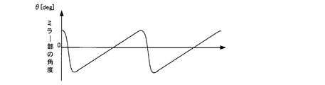
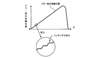
- the signal waveform for driving the mirror portion of the optical scanning element includes a resonance frequency unique to the optical scanning element, resonance vibration occurs in the optical scanning element. If the resonance component causes the inherent resonance component to be superimposed on the oscillation of the mirror portion, the oscillation speed of the mirror portion will fluctuate, resulting in a situation where optical scanning cannot be performed properly (see FIG. 13).
- the drive signal for driving the mirror portion of the optical scanning element is generated by performing a filtering process using a low-pass filter or the like.
- the linearity of the waveform cannot be ensured strictly. For this reason, it may be difficult to drive the mirror portion with high accuracy at a constant angular velocity during the period of scanning the light beam.
- the calculation load is large because a high-order low-pass filter is used.
- the present invention has been made in view of the above-described problems, and reduces the calculation load for generating the drive signal waveform while improving the linearity of the drive signal waveform in the scanning period of the light beam.
- An object of the present invention is to provide an optical scanning device and an image display device that can perform the above-described operation.
- a non-resonant type light having a mirror portion supported by a beam portion from both sides and capable of swinging the mirror portion by twisting displacement of the beam portion.
- the control unit converts the waveform of the drive signal into a sawtooth waveform,
- the waveform during the period in which the light beam is scanned is a linear waveform
- the differential waveform during the period in which the light beam is not scanned is combined with the waveform of one cycle of one frequency or the waveform of a half cycle of two frequencies.
- the mirror unit can be swung with high accuracy at a constant speed, and in the period during which the light beam is not scanned, Since the waveform is formed by connecting the end portions of the half-cycle waveform of the first frequency and the half-cycle waveform of the second frequency, the calculation load can be reduced.
- the waveform of the period during which the light beam is not scanned is formed by a waveform of one cycle of one frequency
- ⁇ L is a differential value of the linear waveform of the sawtooth waveform
- Tch is Of the sawtooth waveform
- the time at the start of the period in which the light beam is not scanned is set
- ⁇ is the ratio (% / 100) of the section of the linear waveform in the sawtooth waveform
- ⁇ m is the maximum amplitude of the drive signal
- the differential value ⁇ (t) of the signal level of the drive signal is May be satisfied.
- the waveform of the period during which the light beam is not scanned is formed by combining the first waveform and the second waveform of a half cycle of two frequencies, and ⁇ L is included in the sawtooth waveform
- Tch is the time at the start of the period in which the luminous flux is not scanned in the sawtooth waveform
- ⁇ is the ratio (% / 100) of the section of the linear waveform in the sawtooth waveform
- ⁇ is the ratio (% / 100) of the first waveform to the first waveform and the second waveform
- ⁇ m is the maximum amplitude of the drive signal
- f is the reciprocal of one period of the sawtooth waveform.
- the optical scanning device further includes a detection unit that detects the displacement of the mirror unit, and the control unit includes a displacement command based on a waveform of the drive signal and a displacement of the mirror unit detected by the detection unit. It is also possible to perform feedback control for detecting the error amount and correcting the drive signal based on the error amount.
- a light source that emits a light beam having an intensity corresponding to an image signal
- a first optical scanning element that scans the light beam emitted from the light source in a first direction at a relatively high speed.
- a mirror part supported by the beam part from both sides, and the mirror part is swung around the swing axis by the torsional displacement of the beam part, and the light beam scanned by the first scanning element is caused by the mirror part.
- An image comprising: a non-resonant type second optical scanning element that scans relatively slowly in a second direction substantially orthogonal to the first direction; and a control unit that controls the first and second optical scanning elements.
- the control unit sets a waveform of a drive signal for swinging the mirror unit of the second optical scanning element as a sawtooth waveform, and out of the sawtooth waveform, a waveform of a period during which the light beam is scanned is a linear waveform.
- the differential waveform of the waveform during the period when the beam is not scanned A period in which one end of a waveform of one frequency or a half period of two frequencies is combined with each other, and both ends of the waveform in a period in which the light flux is not scanned are scanned with the light flux Forming a waveform during a period in which the light beam is not scanned so as to have the same inclination as that of the waveform, and recognizing both ends of the waveform in the period during which the light beam is not scanned, respectively. It is made to continue.
- FIG. 5 is an equivalent circuit of a detection unit configured by the piezoresistive element shown in FIG. 4.
- FIG. It is a figure which shows the change of the resistance value of a piezoresistive element by the displacement of the beam part of the optical scanning element shown in FIG. It is a figure which shows the structure of the control part shown in FIG.
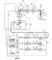
- FIG. 1 is a diagram showing a configuration of an optical scanning device
- FIG. 2 is a diagram showing a waveform of a drive signal
- FIG. 3 is a diagram showing a change in angle of a mirror section.
- the optical scanning device 1 includes a control unit 2 that controls the entire optical scanning device 1 and a light source unit 3 that emits a light beam having an intensity corresponding to a drive signal Sa output from the control unit 2. And an optical scanning element 4 that scans the light beam emitted from the light source unit 3 in a predetermined direction.
- the control unit 2 generates a drive signal Sb that is a drive current for forcibly driving the mirror unit 10 of the optical scanning element 4 in a non-resonant manner, and the current waveform is a sawtooth waveform.
- a signal Sb is applied to the optical scanning element 4.
- the sawtooth drive signal Sb is a signal in which the period of transition from the maximum level to the minimum level is sufficiently shorter than the period of transition from the minimum level to the maximum level.
- the mirror unit 10 of the optical scanning element 4 is configured to rotate around the swing axis Ly at an angle corresponding to the signal level of the drive signal Sb.
- the mirror unit 10 of the optical scanning element 4 is shown in FIG. As shown, it swings in a sawtooth shape around a swing axis Ly described later based on the signal waveform of the drive signal Sb.
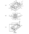
- FIG. 4 is a diagram showing a specific configuration of the optical scanning element 4.
- the optical scanning element 4 includes a mirror part 10 having a reflecting surface 10a, a pair of beam parts 11a and 11b, a pair of support parts 12a and 12b, a fixed part 13a, 13b and a base 14, and the mirror 10 is swung around the swing axis Ly to scan the light flux.
- the pair of beam portions 11a and 11b extends along the swing axis Ly and supports each side of the mirror portion 10 with elasticity, and the mirror portion 10 is supported by the swing displacement Ly by its torsional displacement (twist deformation). It can swing around. Further, the pair of support portions 12a and 12b support the other ends of the pair of beam portions 11a and 11b with elasticity at the central portion thereof, and both fixed portions 13a and 13b fixed to the base 14 at both ends. It is fixed to. Thus, the mirror part 10 is supported by the pair of beam parts 11a and 11b and the pair of support parts 12a and 12b so as to be swingable.
- Permanent magnets 15a and 15b are arranged close to two sides parallel to the swing axis Ly of the mirror unit 10.
- the direction of the magnetic field formed by the permanent magnets 15a and 15b is parallel to the reflecting surface 10a of the mirror unit 10 in a stationary state and is perpendicular to the swing axis Ly.
- a coil 16 is formed on the back surface of the mirror portion 10 opposite to the reflecting surface 10a.
- the electrode of the coil 16 is connected to the control unit 2 via two beam portions 11a and 11b.
- a Lorentz force acts on the lower half of the coil 16 from the swing axis Ly in the drawing as viewed from the front side of the paper, and a Lorentz force acts on the back side of the paper as viewed from the drawing. .
- a rotational torque is generated in the mirror portion 10 about the swing axis Ly. Therefore, by controlling the magnitude of the current of the drive signal Sb output from the control unit 2, the angle around the swing axis Ly of the mirror unit 10 can be controlled.
- the optical scanning element 4 is further provided with piezoresistive elements R1 to R4 as a detection unit 18 for detecting an angle around the swing axis Ly of the mirror unit 10.
- the pair of piezoresistive elements R1 and R3 are disposed symmetrically with respect to the swing axis Ly on the support portion 12a.
- the piezoresistive element R1 is arranged on the support part 12a on the fixed part 13a side, and the piezoresistive element R3 is arranged on the support part 12a on the fixed part 13b side.
- the pair of piezoresistive elements R2 and R4 are disposed symmetrically with respect to the swing axis Ly on the support portion 12b.
- the piezoresistive element R2 is arranged on the support part 12b on the fixed part 13a side, and the piezoresistive element R4 is arranged on the support part 12b on the fixed part 13b side.
- the resistance value of one pair of piezoresistive elements R1 and R3 changes depending on the stress field generated in the vicinity of the swing axis Ly according to the torsional displacement generated in the beam portion 11a, and the other pair of piezoresistive elements.
- the resistance values of the elements R2 and R4 change depending on the stress field generated in the vicinity of the swing axis Ly according to the torsional displacement generated in the beam portion 11b.
- the pair of piezoresistive elements R1 and R3 are arranged in series between the power supply potential Vc and the ground potential GND.
- the pair of piezoresistive elements R4 and R2 are arranged in series with the power supply potential Vc and the ground potential GND. That is, one end of the piezoresistive elements R1 and R4 is connected to the power supply of the power supply potential Vc, and the other end is connected to one end of the piezoresistive elements R2 and R3. The other ends of the piezoresistive elements R2 and R3 are connected to the ground of the ground potential GND.
- FIG. 5 is an equivalent circuit of the detection unit 18 constituted by the piezoresistive elements R1 to R4 shown in FIG. 4 (c).
- the detection unit 18 uses a connection point between a pair of piezoresistive elements R1 and R3 as a first output node N1, and a connection point between the other pair of piezoresistive elements R4 and R2 as a second output node. N2.
- each of the piezoresistive elements R1 to R4 has a characteristic in which the resistance value increases due to compressive stress and the resistance value decreases due to tensile stress
- the resistance value is as follows due to the displacement of the mirror portion 10. Changes.
- the piezoresistive elements R1 to R4 have the same material and the same shape, and the same characteristics.
- the resistance values of the piezoresistive elements R1 and R2 increase due to the compressive stress, and the piezoresistive resistance is increased.
- the resistance values of the elements R3 and R4 decrease due to the tensile stress. Therefore, the voltage VPR + at the first output node N1 decreases, the voltage VPR ⁇ at the second output node N2 increases, and the detection voltage Vd becomes positive.
- the detection voltage Vd increases as the angle ⁇ of the mirror unit 10 around the swing axis Ly increases.
- the detection voltage Vd becomes negative, and the detection is performed as the angle of the mirror section 10 about the swing axis Ly increases.
- the voltage Vd increases.
- the inclination direction of the mirror unit 10 from the equilibrium state shown in FIG. 4 can be found from the polarity of the detection voltage Vd, and the inclination angle of the mirror unit 10 can be found from the magnitude of the detection voltage Vd.
- the control unit 2 detects the actual tilt angle of the mirror unit 10 around the swing axis Ly by the detection voltage Vd.
- control unit 2 generates the drive signal Sb, swings the mirror unit 10 about the swing axis Ly, and reflects the light beam by the reflecting surface 10a of the mirror unit 10 to scan the light beam.
- the configuration is as shown in FIG.
- control unit 2 includes a target command generation unit 21, a comparison dimension conversion unit 22, a subtraction unit 23, and a drive signal generation unit 24.
- the target command generation unit 21 outputs the target angle of the mirror unit 10 according to the direction to be scanned by the optical scanning element 4 as a target angle command.
- the optical scanning device 1 is driven so that the angle of the mirror portion 10 of the optical scanning element 4 is displaced in a sawtooth shape as shown in FIG. 3 by a sawtooth drive signal Sb (see FIG. 2).
- the unit 21 sequentially outputs a target angle command from the target command generating unit 21 so that the angle of the mirror unit 10 is displaced in a sawtooth shape as shown in FIG.
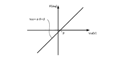
- the comparison dimension conversion unit 22 stores a specified value ⁇ and an offset value ⁇ that define the relationship between the target angle of the mirror unit 10 and the control voltage Vct, and responds to the target angle command output from the target command generation unit 21.
- the control voltage Vct is output.
- the specified value ⁇ and the offset value ⁇ are used to generate the control voltage Vct so that feedback control can be performed by the detection voltage Vd.
- the control voltage Vct and the angle of the mirror unit 10 are in a proportional relationship, and the control voltage Vct is based on the following equation (1) based on the target angle ⁇ . Is calculated.
- the comparison dimension conversion unit 22 stores therein a conversion table that defines the relationship between the target angle of the mirror unit 10 and the control voltage Vct, and the target angle of the mirror unit 10 is determined based on this conversion table. You may make it convert into Vct.
- the subtracting unit 23 subtracts the voltage value of the detection voltage Vd from the voltage value of the control voltage Vct, calculates the differential voltage Vs between the control voltage Vct and the detection voltage Vd, and outputs the differential voltage Vs.
- the drive signal generator 24 generates a drive signal Sb whose current value is increased or decreased according to the differential voltage Vs, and outputs this drive signal Sb to the coil 16 of the optical scanning element 4. That is, when the differential voltage Vs is positive, the drive signal Sb is generated by increasing the current value by a value proportional to the voltage level of the differential voltage Vs. When the differential voltage Vs is negative, the differential voltage Vs is generated. The drive signal Sb is generated by reducing the current value by a value proportional to the voltage level.
- the drive signal generator 24 can be configured by an integrator that integrates the differential voltage Vs, for example.
- the optical scanning element 4 is driven by the drive signal Sb having a current value corresponding to the differential voltage Vs to perform feedback control, whereby the angular displacement of the mirror portion 10 of the optical scanning element 4 is shown in FIG.
- the mirror unit 10 is swung with high accuracy so as to have a sawtooth shape.
- control unit 2 calculates an error between the target angle command (displacement command) by the target command generation unit 21 based on the waveform of the drive signal and the angle (displacement) of the mirror unit 10 detected by the detection unit 18.
- the feedback control for detecting and correcting the drive signal Sb based on the error is performed. Thereby, the mirror part 10 of the optical scanning element 4 is swung with high accuracy.
- the optical scanning element 4 scans the light beam incident on the reflecting surface 10a of the mirror unit 10 when the mirror unit 10 swings around the swing axis Ly (see FIG. 6A).
- the optical scanning element 4 has a resonance mode in which the mirror unit 10 resonates at a predetermined frequency.
- a resonance mode of longitudinal vibration in which the mirror unit 10 swings in a direction orthogonal to the reflecting surface 10a (FIG. 6B), or resonance of lateral vibration in which the mirror unit 10 swings in a direction parallel to the reflecting surface 10a.
- the optical scanning element 4 has a resonance mode
- the drive signal Sb for driving the optical scanning element 4 includes a resonance frequency component unique to the optical scanning element 4
- the optical scanning element 4 The resonance frequency component is superimposed on the oscillation of the mirror unit 10 (see FIG. 13).
- the sawtooth waveform signal is subjected to filtering processing by a low-pass filter.
- the calculation load is large because a high-order low-pass filter is used.
- the mirror unit 10 cannot be displaced with high accuracy at a constant angular velocity. That is, if the sawtooth drive signal is filtered by a low-pass filter, the signal waveform becomes dull as shown in FIG. 9, and the mirror portion cannot be displaced with high accuracy at a constant angular velocity during the light beam scanning period. .
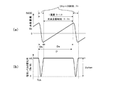
- the target command generation unit 21 sets the waveform of the drive signal Sb as a sawtooth waveform D, and among the sawtooth waveform D, sets the waveform of the light beam scanning period as a linear waveform Da.
- the waveform Db during a period in which the light beam is not scanned (hereinafter referred to as a retrace period) has a first waveform D1 whose differential waveform is a half cycle of the first frequency f1, and a differential waveform thereof is a half cycle of the second frequency f2.
- a waveform Db of a period in which the light beam is not scanned is formed such that the waveform is a combination of the second waveform D2 and both ends of the waveform Db in the retrace period have the same inclination as the inclination of the waveform Da in the light beam scanning period.
- both end portions of the waveform Db in the retrace period (hereinafter referred to as the retrace waveform Db) are made to be continuous with both end portions of the waveform Da in the light beam scanning period.
- the target command generation unit 21 integrates the differential waveform of one cycle of one frequency fa to generate the retrace waveform Db.
- the coupling point between the linear waveform Da and the retrace waveform Db is made to have the same inclination, thereby suppressing the sawtooth waveform D from containing a high frequency component.
- the frequency fa is determined based on the period of the sawtooth waveform D and the linear waveform Da as follows.
- the target command generation unit 21 generates the retrace waveform Db in the retrace period by performing a calculation using a trigonometric function based on the period of the sawtooth waveform D and the linear waveform Da, and integrating the calculation result. To do.
- the inflection value is zero at the connection point between the differential waveform of the linear waveform Da and the differential waveform of the retrace waveform Db, in other words, this connection point takes an extreme value.
- ⁇ L differential value of the signal level of the linear waveform
- Tch time at the start of the retrace period
- ⁇ proportion of the section of the linear waveform Da in the sawtooth waveform
- D % / 100
- the target command generation unit 21 can obtain the calculation result shown in FIG. 10B by calculating this differential value ⁇ (t), and integrating the calculation result as shown in FIG. 10A.
- a drive signal Sb composed of a linear waveform Da and a retrace waveform Db is generated.
- the differential value ⁇ (t) of the signal level of the drive signal Sb is proportional to the angular velocity of the mirror unit 10, and the integral value of the differential value ⁇ (t) means the amount of change in the angle of the mirror unit 10. . Therefore, the high frequency component superimposed on the sawtooth waveform D can be reduced during the light beam scanning period, and the linearity of the drive signal waveform can be improved during the light beam scanning period.
- the drive signal waveform can be generated by a relatively simple calculation using a trigonometric function, the calculation load for the drive signal waveform can be reduced.
- the target command generation unit 21 combines the first waveform D1 whose differential value is a half cycle of the frequency f1 and the second waveform D2 whose differential value is a half cycle of the frequency f2. That is, a retrace waveform Db is generated by integrating a waveform obtained by combining a half cycle waveform of the wave number f1 and a half cycle of the frequency f2.
- the coupling point between the linear waveform Da and the retrace waveform Db and the coupling point between the first waveform D1 and the second waveform D2 are made to have the same inclination, so that the sawtooth waveform D has a high frequency. Including ingredients is suppressed.
- the frequencies f1 and f2 are determined based on the period of the sawtooth waveform D and the linear waveform Da as follows.
- the target command generator 21 generates the retrace waveform Db by performing a calculation using a trigonometric function based on the period of the sawtooth waveform D and the linear waveform Da, and integrating the calculation result.
- the inflection value is zero at the connection point between the differential waveform of the linear waveform Da and the differential waveform of the retrace waveform Db, in other words, this connection point takes an extreme value.
- the linear waveform Da, the first waveform D1, and the second waveform D2 are calculated.
- ⁇ L differential value of the signal level of the linear waveform Da
- Tch time at the start of the retrace period
- ⁇ proportion of the section of the linear waveform Da in the sawtooth waveform D (% / 100)
- ⁇ Ratio of the section of the first waveform D1 in the section of the retrace waveform Db (% / 100)
- ⁇ m Maximum amplitude of drive signal Sb f: Reciprocal of one period T of sawtooth waveform D
- the target command generation unit 21 can obtain the calculation result shown in FIG. 11B by calculating the differential value ⁇ (t), and integrates the calculation result as shown in FIG. 11A.
- a drive signal Sb composed of a linear waveform Da and a retrace waveform Db is generated.
- the differential value ⁇ (t) of the signal level of the drive signal Sb is proportional to the angular velocity of the mirror unit 10, and the integral value of the differential value ⁇ (t) means the amount of change in the angle of the mirror unit 10. . Therefore, the high frequency component superimposed on the sawtooth waveform D can be reduced during the light beam scanning period, and the linearity of the drive signal waveform can be improved during the light beam scanning period.
- the drive signal waveform can be generated by a relatively simple calculation using a trigonometric function, the calculation load for the drive signal waveform can be reduced.
- the image display apparatus 100 includes a control unit 110, a light source unit 120, a scanning unit 140, a second relay optical system 180, a half mirror 185, and the like.
- the control unit 110 includes a drive signal supply unit 111, a main scanning drive signal generation unit 112, a sub-scanning drive signal generation unit 113, and a main control unit 114.
- the drive signal supply unit 111 receives RGB pixel signals 115r, 115g, and 115b for the three primary colors that are elements for forming an image. Generated in pixel units.
- the main scanning drive signal generating unit 112 generates and outputs a main scanning driving signal 116 used in the main scanning unit 160 so that an optical scanning element 161 (described later) of the main scanning unit 160 is in a predetermined scanning range in a resonance state.
- the sub-scanning drive signal generation unit 113 generates and outputs a sawtooth-shaped sub-scanning drive signal 117 used in the sub-scanning unit 170 based on the frequency of the main scanning drive signal 116.
- the light source unit 120 is provided with an R laser driver 121, a G laser driver 122, and a B laser driver 123.
- the laser drivers 121, 122, and 123 supply drive currents to the lasers 124, 125, and 126 based on the R, G, and B drive signals 115r, 115g, and 115b output from the drive signal supply unit 111, respectively.
- Each laser 124, 125, 126 emits laser light whose intensity is modulated in accordance with the drive current supplied from each laser driver 121, 122, 123.
- the R (red) laser light Lr, G (green) laser light Lg, and B (blue) laser light Lb emitted from the lasers 124, 125, and 126 were collimated by collimating optical systems 127, 128, and 129, respectively. Later, the light enters the dichroic mirrors 130, 131, and 132. Thereafter, the laser beams Lr, Lg, and Lb of the three primary colors are wavelength-selectively reflected and transmitted by these dichroic mirrors 130, 131, and 132, reach the coupling optical system 133, and are combined to the optical fiber cable 135. Emitted.
- the laser light emitted to the optical fiber cable 135 is a combination of intensity-modulated laser light of each color.
- the scanning unit 140 includes a collimating optical system 151, a main scanning unit 160, a first relay optical system 165, a sub-scanning unit 170, and the like.
- the collimating optical system 151 converts the laser light generated by the light source unit 120 and emitted through the optical fiber cable 135 into parallel light.
- the main scanning unit 160 and the sub-scanning unit 170 are arranged in the main scanning direction and the sub-scanning direction so that the laser light incident from the optical fiber cable 135 can be projected onto the retina 190b of the user's eye 190 as an image.
- An optical system for scanning The main scanning unit 160 includes an optical scanning element 161 that reciprocally scans incident laser light that has been collimated by the collimating optical system 151 in the main scanning direction.
- the sub-scanning unit 170 scans the optical scanning element 171 that scans in the main scanning direction by the main scanning unit 160 and scans the laser light incident through the first relay optical system 165 at a relatively low speed in the sub-scanning direction.
- This sub-scanning direction is a direction substantially orthogonal to the main scanning direction.
- the main scanning direction can be the horizontal direction and the sub-scanning direction can be the vertical direction.
- the first relay optical system 165 that relays the laser beam between the main scanning unit 160 and the sub-scanning unit 170 converges the laser beam scanned in the main scanning direction by the optical scanning element 161 on the mirror unit of the optical scanning element 171.
- the laser beam is scanned in the sub-scanning direction by the optical scanning element 171.
- the laser beam scanned by the optical scanning element 171 is a half mirror 185 positioned in front of the eye 190 via a second relay optical system 180 in which two lenses 180a and 180b having positive refractive power are arranged in series. And is incident on the user's pupil 190a.
- the image display device 100 is a see-through retinal scanning image display device that forms an image on the retina of the user's eye 190 by superimposing an image according to the image signal S and an outside scene.
- the optical scanning element 171 has the same configuration as that of the optical scanning element 4, and the sub-scanning drive signal generation unit 113 includes the control unit 2 of the optical scanning device 1 described above. Similarly, the optical scanning element 171 is driven. Therefore, the mirror unit 10 can be driven with high accuracy at a constant angular velocity during the period of scanning the light beam, and the calculation load can be reduced.
- laser light that is advantageous in terms of efficiency is used as an example of light flux, but the light flux is not limited to laser light.
- the detection unit for detecting the angle of the mirror part of the optical scanning element is configured by a piezoresistive element, a detection method using a piezoelectric element or a detection method using a change in capacitance may be used.
- the mirror portion 10 is supported by the beam portions 11a and 11b from both sides, and the mirror portion is caused by the torsional displacement of the beam portions 11a and 11b.
- the differential waveform of the waveform Db is a waveform of one cycle of one frequency, or a waveform obtained by combining waveforms of half cycles of two frequencies, and both ends of the waveform of a period in which the light beam is not scanned are respectively
- the luminous flux A waveform for a period in which the light beam is not scanned is formed so as to have the same inclination as the shape inclination, and both end portions of the waveform in the period in which the light beam is not scanned are respectively connected to both end portions of the waveform in the period during which the light beam is scanned. Therefore, the high frequency component superimposed on the sawtooth waveform D can be reduced during the light beam scanning period, and the linearity of the drive signal waveform can be improved.
- the calculation load at the time of the drive signal waveform can be reduced.
- the detection part 18 which detects the displacement of the mirror part 10 is provided, and the control part 2 (110) is based on the waveform of the drive signal Sb (117), and the displacement of the mirror part 10 detected by the detection part 18 And the feedback control for correcting the drive signal Sb (117) based on the error is performed, so that the mirror unit 10 of the optical scanning element 4 (171) can be oscillated with high accuracy.
Landscapes
- Physics & Mathematics (AREA)
- General Physics & Mathematics (AREA)
- Optics & Photonics (AREA)
- Mechanical Optical Scanning Systems (AREA)
- Facsimile Scanning Arrangements (AREA)
- Micromachines (AREA)
- Facsimile Heads (AREA)
Abstract
光束を走査する期間において、駆動信号波形の直線性を向上させつつも、駆動信号波形生成のための演算負荷を小さくする。両側から梁部で支持されたミラー部を有し、梁部の捻れ変位によりミラー部を揺動可能とした非共振型の光走査素子と、駆動信号によりミラー部を揺動させる制御部と、を備え、制御部は、駆動信号の波形を鋸波状波形Dとし、当該鋸波状波形Dのうち、光束を走査する期間の波形を直線波形Daとする一方、光束を走査しない期間の波形Dbの微分波形が、一つの周波数の1周期の波形、又は、2つの周波数の半周期の波形を互いに結合した波形、となり、かつ、当該光束を走査しない期間の波形の両端部のそれぞれが、光束を走査する期間の波形の傾きと同じ傾きとなるように光束を走査しない期間の波形を形成し、光束を走査しない期間の波形の両端部のそれぞれを光束を走査する期間の波形の両端部のそれぞれに連続させた。
Description
本発明は、入射する光束を反射面が形成されたミラー部により所定方向に走査する光走査素子を備えた光走査装置及び画像表示装置に関する。
従来より、入射する光束を反射面が形成されたミラー部により所定方向に走査する光走査素子と、駆動信号により光走査素子のミラー部を揺動軸回りに揺動させる制御部と、を備えた光走査装置や画像表示装置が知られている。
このような光走査装置や画像表示装置に用いられる光走査素子として、梁部で支持されたミラー部を有し、梁部の捻れ変位によりミラー部を揺動軸回りに揺動させてミラー部により光束を走査する光走査素子が知られている(例えば、特許文献1参照)。
しかし、このような光走査素子においては、ミラー部は弾性のある梁部を介して支持部に揺動可能に支持されているため、ミラー部及び梁部で決まる固有の共振周波数が存在してしまう。
このように、光走査素子のミラー部を駆動する信号波形に光走査素子固有の共振周波数が含まれていると、光走査素子において共振振動が発生する。そして、この共振振動によりミラー部の揺動に固有共振の成分が重畳すると、ミラー部の揺動速度が変動してしまい、光走査を適切に行なうことができない事態が生じる(図13参照)。
そこで、従来の光走査装置や画像表示装置では、光走査素子のミラー部を駆動する駆動信号を、ローパスフィルタなどにより前記共振周波数の成分を抑圧するようなフィルタリング処理を行なって生成することにより、共振振動を抑制している(特許文献2参照)。
しかしながら、従来の光走査装置や画像表示装置では、光走査素子のミラー部を駆動する駆動信号を、ローパスフィルタなどによりフィルタリング処理を行って生成しているため、光束を走査する期間において、駆動信号波形の直線性が厳密には確保できておらず、そのため、光束を走査する期間において、一定の角速度でミラー部を高精度に駆動することが困難となる場合がある。しかも、高次のローパスフィルタを用いているために演算負荷が大きいという問題もある。
本発明は、上述したような課題に鑑みてなされたものであり、光束を走査する期間において、駆動信号波形の直線性を向上させつつも、駆動信号波形生成のための演算負荷を小さくすることができる光走査装置及び画像表示装置を提供することを目的とする。
上記目的を達成するために、本発明の1つの態様では、両側から梁部で支持されたミラー部を有し、前記梁部の捻れ変位によりミラー部を揺動可能とした非共振型の光走査素子と、駆動信号を生成して前記ミラー部を揺動させる制御部と、を備えた光走査装置において、前記制御部は、前記駆動信号の波形を鋸波状波形とし、当該鋸波状波形のうち、光束を走査する期間の波形を直線波形とする一方、光束を走査しない期間の波形の微分波形が、一つの周波数の1周期の波形、又は、2つの周波数の半周期の波形を互いに結合した波形、となり、かつ、当該光束を走査しない期間の波形の両端部のそれぞれが、光束を走査する期間の波形の傾きと同じ傾きとなるように前記光束を走査しない期間の波形を形成し、前記光束を走査しない期間の波形の両端部のそれぞれを前記光束を走査する期間の波形の両端部のそれぞれに連続させている。
このように、光束を走査する期間において、駆動信号の波形を直線形状としたため、一定の速度でミラー部を高精度に揺動することができ、しかも、光束を走査しない期間において、駆動信号の波形を、第1周波数の半周期の波形と、第2周波数の半周期の波形とを端部同士を結合することにより形成したので、演算負荷を小さくすることができる。
また、前記光走査装置において、前記光束を走査しない期間の波形を、一つの周波数の1周期の波形により形成しており、ωLを前記鋸波状波形のうち前記直線波形の微分値とし、Tchを前記鋸波状波形のうち光束を走査しない期間の開始時点の時間とし、αを前記鋸波状波形のうち前記直線波形の区間の割合(%/100)とし、θmを前記駆動信号の最大振幅とし、fを前記鋸波状波形の1周期の逆数としたとき、前記駆動信号の信号レベルの微分値ω(t)は、
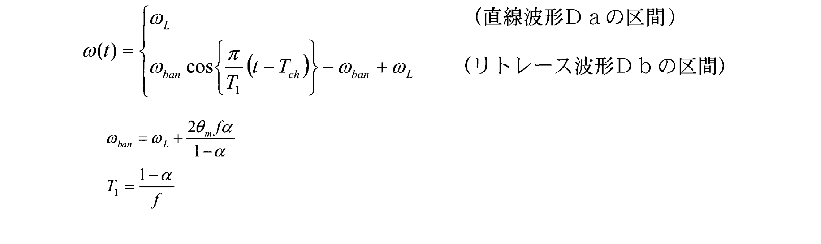
を満たしていてもよい。
を満たしていてもよい。
また、前記光走査装置において、前記光束を走査しない期間の波形を、2つの周波数の半周期の第1波形と第2波形を結合した波形により形成しており、ωLを前記鋸波状波形のうち前記直線波形の微分値とし、Tchを前記鋸波状波形のうち光束を走査しない期間の開始時点の時間とし、αを前記鋸波状波形のうち前記直線波形の区間の割合(%/100)とし、βを前記第1波形及び第2波形の区間のうち前記第1波形の区間の割合(%/100)とし、θmを前記駆動信号の最大振幅とし、fを前記鋸波状波形の1周期の逆数としたとき、前記駆動信号の信号レベルの微分値ω(t)は、
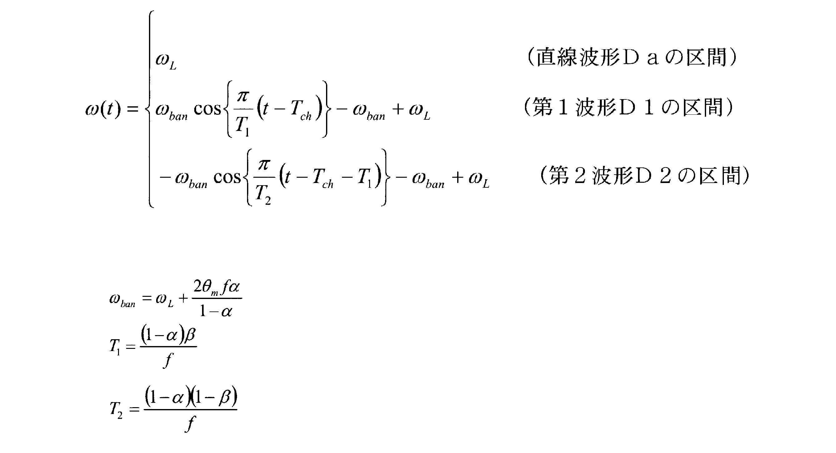
を満たしていてもよい。
を満たしていてもよい。
また、前記光走査装置において、前記ミラー部の変位を検出する検出部を備え、前記制御部は、前記駆動信号の波形を基にした変位指令と前記検出部で検出した前記ミラー部の変位との誤差分を検出し、その誤差分に基づいて駆動信号を補正するフィードバック制御を行ってもよい。
また、本発明のもう1つの態様においては、画像信号に応じた強度の光束を出射する光源と、前記光源から出射された光束を第1方向に相対的に高速に走査する第1光走査素子と、両側から梁部で支持されたミラー部を有し、前記梁部の捻れ変位によりミラー部を揺動軸回りに揺動させて前記第1走査素子により走査された光束を前記ミラー部により第1方向と略直交する第2方向に相対的に低速に走査する非共振型の第2光走査素子と、前記第1及び第2の光走査素子を制御する制御部と、を備えた画像表示装置において、前記制御部は、前記第2の光走査素子のミラー部を揺動させる駆動信号の波形を鋸波状波形とし、当該鋸波状波形のうち、光束を走査する期間の波形を直線波形とする一方、光束を走査しない期間の波形の微分波形が、一つの周波数の1周期の波形、又は、2つの周波数の半周期の波形を互いに結合した波形、となり、かつ、当該光束を走査しない期間の波形の両端部のそれぞれが、光束を走査する期間の波形の傾きと同じ傾きとなるように前記光束を走査しない期間の波形を形成し、前記光束を走査しない期間の波形の両端部のそれぞれを前記光束を走査する期間の波形の両端部のそれぞれに連続させている。
[1.光走査装置]
以下に、本発明に好適な実施形態について図面に基づいて説明する。以下の説明では、まず、光走査装置について説明し、その後、画像表示装置について説明する。
以下に、本発明に好適な実施形態について図面に基づいて説明する。以下の説明では、まず、光走査装置について説明し、その後、画像表示装置について説明する。
[1.1.光走査装置の概要]
まず、本実施形態に係る光走査装置について説明する。図1は光走査装置の構成を示す図、図2は駆動信号の波形を示す図、図3はミラー部の角度変化を示す図である。
まず、本実施形態に係る光走査装置について説明する。図1は光走査装置の構成を示す図、図2は駆動信号の波形を示す図、図3はミラー部の角度変化を示す図である。
図1に示すように、光走査装置1は、当該光走査装置1全体を制御する制御部2と、この制御部2から出力される駆動信号Saに応じた強度の光束を出射する光源部3と、この光源部3から出射された光束を所定方向に走査する光走査素子4とを備えている。
制御部2は、光走査素子4のミラー部10を非共振で強制的に駆動する駆動電流であって、その電流波形が鋸波状波形となる駆動信号Sbを生成するものであり、生成した駆動信号Sbを光走査素子4に印加する。鋸波状の駆動信号Sbは、図2に示すように、最小レベルから最大レベルまで移行する期間に比べ、最大レベルから最小レベルへ移行する期間が十分に短い信号である。光走査素子4のミラー部10は、駆動信号Sbの信号レベルに応じた角度で揺動軸Ly回りに回動するように構成されており、光走査素子4のミラー部10は、図3に示すように、駆動信号Sbの信号波形に基づいて後述する揺動軸Ly回りに鋸波状に揺動する。
[1.2.光走査素子の具体的構成]
次に、光走査素子4の具体的構成について説明する。図4は光走査素子4の具体的構成を示す図である。
次に、光走査素子4の具体的構成について説明する。図4は光走査素子4の具体的構成を示す図である。
図4(a)に示すように、光走査素子4は、反射面10aが形成されたミラー部10と、一対の梁部11a、11bと、一対の支持部12a,12bと、固定部13a,13bと、基台14とを有しており、ミラー部10を揺動軸Ly回りに揺動させて、光束を走査する。
一対の梁部11a、11bは、揺動軸Lyに沿って延伸してミラー部10の両側のそれぞれを弾性を持って支持し、その捻れ変位(捻れ変形)によりミラー部10を揺動軸Ly回りに揺動可能としている。また、一対の支持部12a,12bは、一対の梁部11a,11bのそれぞれの他端をその中央部で弾性を持って支持すると共に両端部が基台14に固着された固定部13a,13bに固定されている。このように、ミラー部10は一対の梁部11a、11bと一対の支持部12a,12bとによりに揺動可能に支持されている。
ミラー部10の揺動軸Lyに平行な2辺に近接して永久磁石15a,15bが配置されている。永久磁石15a,15bが形成する磁界の向きは、静止状態のミラー部10の反射面10aに平行で、揺動軸Lyに直交する方向である。また、図4(b)に示すように、ミラー部10の反射面10aと反対側の裏面にはコイル16が形成されている。コイル16の電極は2つの梁部11a,11bを介して制御部2に接続される。この構成により、コイル16に駆動電流を流すとコイル16にローレンツ力が働く。図面視で揺動軸Lyから下半分のコイル16には例えば紙面の表面側にローレンツ力が働き、図面視で揺動軸Lyから上半分のコイル16には紙面の裏面側にローレンツ力が働く。これにより、ミラー部10には揺動軸Lyを中心として回転トルクが生ずる。従って、制御部2から出力する駆動信号Sbの電流の大きさを制御することにより、ミラー部10の揺動軸Ly回りの角度を制御することができる。
この光走査素子4には、さらに、ミラー部10の揺動軸Ly回りの角度を検出する検出部18として、ピエゾ抵抗素子R1~R4が設けられる。一対のピエゾ抵抗素子R1,R3は、支持部12a上に揺動軸Lyに対して対称配置される。ピエゾ抵抗素子R1は固定部13a側の支持部12a上に配置されており、ピエゾ抵抗素子R3は固定部13b側の支持部12a上に配置されている。同様に、一対のピエゾ抵抗素子R2,R4は、支持部12b上に揺動軸Lyに対して対称配置される。ピエゾ抵抗素子R2は固定部13a側の支持部12b上に配置されており、ピエゾ抵抗素子R4は固定部13b側の支持部12b上に配置されている。
そして、一方の一対のピエゾ抵抗素子R1,R3は、梁部11aに発生する捻れ変位に応じて揺動軸Ly近傍に発生する応力場によって各々その抵抗値が変化し、他方の一対のピエゾ抵抗素子R2,R4は、梁部11bに発生する捻れ変位に応じて揺動軸Ly近傍に発生する応力場によって各々その抵抗値が変化する。
図4(c)に示すように、一対のピエゾ抵抗素子R1,R3は、電源電位Vcと接地電位GND間に直列に配置される。また、同様に、一対のピエゾ抵抗素子R4,R2は、電源電位Vcと接地電位GNDに直列に配置される。すなわち、ピエゾ抵抗素子R1,R4の一端が電源電位Vcの電源に接続され、他端がピエゾ抵抗素子R2,R3の一端に接続される。ピエゾ抵抗素子R2,R3の他端は、接地電位GNDのグランドに接続される。
図5は、図4(c)に示すピエゾ抵抗素子R1~R4により構成される検出部18の等価回路である。この検出部18は、同図に示すように、一対のピエゾ抵抗素子R1,R3の接続点を第1出力ノードN1とし、他の一対のピエゾ抵抗素子R4,R2の接続点を第2出力ノードN2としている。そして、制御部2は、第1出力ノードN1の電圧VPR+と第2出力ノードN2の電圧VPR-とを入力しており、第2出力ノードN2の電圧を基準とした第1出力ノードN1の電圧を検出電圧Vd(=[VPR+]-[VPR-])としている。なお、光走査素子4に駆動信号Sbが印加されていないとき、すなわち駆動信号Sbの電流値が0[A]のとき、ピエゾ抵抗素子R1~R4の抵抗値は変化がなく、ピエゾ抵抗素子R1~R4の初期抵抗値が同一の場合には、検出電圧Vdは0Vとなる。
ここで、各ピエゾ抵抗素子R1~R4は、圧縮応力によりその抵抗値が上昇し、引張応力によりその抵抗値が下降する特性を有するものとすると、ミラー部10の変位により以下のように抵抗値が変化する。なお、ここでは、各ピエゾ抵抗素子R1~R4は、同一材料及び同一形状であり、その特性は同一であるものとする。
例えば、図6(a)に示すように、ミラー部10に揺動軸Ly回りの角度θの傾きが生じたとき、ピエゾ抵抗素子R1,R2は圧縮応力によりその抵抗値が上昇し、ピエゾ抵抗素子R3,R4はその引張応力によりその抵抗値が下降する。そのため、第1出力ノードN1の電圧VPR+は下降し、第2出力ノードN2の電圧VPR-は上昇して、検出電圧Vdは正極性となる。そして、揺動軸Ly回りのミラー部10の角度θが大きくなるほど、検出電圧Vdが大きくなる。一方、図6に示す方向とは逆方向にミラー部10が揺動軸Ly回りに傾いたとき、検出電圧Vdは負極性となり、揺動軸Ly回りのミラー部10の角度が大きくなるほど、検出電圧Vdが大きくなる。
このように、検出電圧Vdの極性により、図4に示す平衡状態からのミラー部10の傾き方向がわかり、検出電圧Vdの大きさによりミラー部10の傾き角がわかる。この原理を利用して、制御部2は、揺動軸Ly回りのミラー部10の実際の傾き角を検出電圧Vdにより検出している。
[1.3.制御部の構成]
制御部2は、上述したように、駆動信号Sbを生成して、ミラー部10を揺動軸Ly回りに揺動させ、ミラー部10の反射面10aにより光束を反射して光束を走査するようにしており、図7に示すように構成されている。
制御部2は、上述したように、駆動信号Sbを生成して、ミラー部10を揺動軸Ly回りに揺動させ、ミラー部10の反射面10aにより光束を反射して光束を走査するようにしており、図7に示すように構成されている。
図7に示すように、制御部2は、目標指令生成部21、比較次元変換部22、減算部23、駆動信号生成部24を有している。
目標指令生成部21は、光走査素子4により走査させようとする方向に応じたミラー部10の目標角度を、目標角度指令として出力する。光走査装置1では、鋸波状の駆動信号Sb(図2参照)により光走査素子4のミラー部10の角度が図3に示すように鋸波状に変位するように駆動しており、目標指令生成部21は、ミラー部10の角度が図3に示すように鋸波状に変位するように、目標角度指令を目標指令生成部21から順次出力する。
比較次元変換部22は、ミラー部10の目標角度と制御電圧Vctとの関係を規定する規定値αとオフセット値βを記憶しており、目標指令生成部21から出力される目標角度指令に応じた制御電圧Vctを出力する。規定値αとオフセット値βは、検出電圧Vdによりフィードバック制御できるように制御電圧Vctを生成するために用いられる。実施形態に係る光走査素子4では、図8に示すように、制御電圧Vctとミラー部10の角度とが比例関係にあり、目標角度θに基づき、以下の式(1)に基づき制御電圧Vctを演算している。
Vct=θ×α+β ・・・(1)
なお、比較次元変換部22において、ミラー部10の目標角度と制御電圧Vctとの関係を規定する変換テーブルを内部に記憶しておき、この変換テーブルに基づき、ミラー部10の目標角度を制御電圧Vctに変換するようにしてもよい。
Vct=θ×α+β ・・・(1)
なお、比較次元変換部22において、ミラー部10の目標角度と制御電圧Vctとの関係を規定する変換テーブルを内部に記憶しておき、この変換テーブルに基づき、ミラー部10の目標角度を制御電圧Vctに変換するようにしてもよい。
減算部23は、制御電圧Vctの電圧値から検出電圧Vdの電圧値を減算して、制御電圧Vctと検出電圧Vdとの差分電圧Vsを演算し、差分電圧Vsを出力する。
駆動信号生成部24は、差分電圧Vsに応じて電流値を増減させた駆動信号Sbを生成し、この駆動信号Sbを光走査素子4のコイル16に出力する。すなわち、差分電圧Vsが正極性の場合には、差分電圧Vsの電圧レベルに比例する値だけ電流値を上げた駆動信号Sbを生成し、差分電圧Vsが負極性の場合には、差分電圧Vsの電圧レベルに比例する値だけ電流値を下げた駆動信号Sbを生成する。この駆動信号生成部24は、例えば、差分電圧Vsを積分する積分器により構成することができる。このように差分電圧Vsに応じた電流値の駆動信号Sbにより光走査素子4を駆動してフィードバック制御するようにしており、これにより光走査素子4のミラー部10の角度変位が図3に示すように鋸波状になるようにミラー部10を精度良く揺動させている。
このように、制御部2は、駆動信号の波形を基にした目標指令生成部21による目標角度指令(変位指令)と検出部18で検出したミラー部10の角度(変位)との誤差分を検出し、その誤差分に基づいて駆動信号Sbを補正するフィードバック制御を行うようにしている。これにより光走査素子4のミラー部10を精度良く揺動するようにしている。
[1.4.駆動信号Sbの生成処理]
光走査素子4は、上述したように、ミラー部10が揺動軸Ly回りに揺動(図6(a)参照)して、ミラー部10の反射面10aに入射する光束を走査するものであるが、この光走査素子4は所定の周波数でミラー部10が共振する共振モードを有している。例えば、ミラー部10が反射面10aと直交する方向へ揺動する縦振動の共振モード(図6(b))や、ミラー部10が反射面10aと平行な方向へ揺動する横振動の共振モード(図6(c))がある。
光走査素子4は、上述したように、ミラー部10が揺動軸Ly回りに揺動(図6(a)参照)して、ミラー部10の反射面10aに入射する光束を走査するものであるが、この光走査素子4は所定の周波数でミラー部10が共振する共振モードを有している。例えば、ミラー部10が反射面10aと直交する方向へ揺動する縦振動の共振モード(図6(b))や、ミラー部10が反射面10aと平行な方向へ揺動する横振動の共振モード(図6(c))がある。
このように、光走査素子4には共振モードがあるため、光走査素子4を駆動する駆動信号Sbに光走査素子4固有の共振周波数成分が含まれている場合には、光走査素子4のミラー部10の揺動に共振周波数の成分が重畳してしまうことになる(図13参照)。
そのため、従来の光走査装置や画像表示装置では、鋸波形信号にローパスフィルタによるフィルタリング処理を行っていた。しかし、高次のローパスフィルタを用いているために演算負荷が大きい。
また、光束を走査する期間(以下、光束走査期間という)において、一定の角速度で高精度にミラー部10を変位させることができない。すなわち、鋸波状の駆動信号にローパスフィルタによるフィルタリング処理を行うと、図9に示すように信号波形が鈍ってしまい、光束走査期間において、一定角速度で高精度にミラー部を変位させることができなくなる。
そこで、上記目標指令生成部21は、図10に示すように、駆動信号Sbの波形を鋸波状波形Dとし、当該鋸波状波形Dのうち、光束走査期間の波形を直線波形Daとする。一方、光束を走査しない期間(以下、リトレース期間という)の波形Dbが、その微分波形が第1周波数f1の半周期となる第1波形D1とその微分波形が第2周波数f2の半周期となる第2波形D2とを結合した波形となり、かつ、リトレース期間の波形Dbの両端部のそれぞれが、光束走査期間の波形Daの傾きと同じ傾きとなるように光束を走査しない期間の波形Dbを形成する。そして、リトレース期間の波形Db(以下、リトレース波形Dbという)の両端部のそれぞれを光束走査期間の波形Daの両端部のそれぞれに連続させるようにしている。
ここで、第1周波数f1と第2周波数f2とは同一周波数(f1=f2)とすることもでき、異なる周波数(f1≠f2)とすることができる。
[1.4.1 f1=f2の場合]
まず、第1周波数f1と第2周波数f2とが同一の周波数faである場合について説明する。この場合、その微分波形が周波数faの半周期となる第1波形とその微分波形が周波数faの半周期となる第2波形とを結合する。すなわち、目標指令生成部21は、一つの周波数faの1周期の微分波形を積分して、リトレース波形Dbを生成する。このとき、直線波形Daとリトレース波形Dbとの結合点は、互いの傾きが同じになるようにすることで、鋸波状波形Dに高周波成分が含まれることを抑制している。この周波数faは、以下のように、鋸波状波形Dの周期と直線波形Daとに基づいて決定されるものである。
まず、第1周波数f1と第2周波数f2とが同一の周波数faである場合について説明する。この場合、その微分波形が周波数faの半周期となる第1波形とその微分波形が周波数faの半周期となる第2波形とを結合する。すなわち、目標指令生成部21は、一つの周波数faの1周期の微分波形を積分して、リトレース波形Dbを生成する。このとき、直線波形Daとリトレース波形Dbとの結合点は、互いの傾きが同じになるようにすることで、鋸波状波形Dに高周波成分が含まれることを抑制している。この周波数faは、以下のように、鋸波状波形Dの周期と直線波形Daとに基づいて決定されるものである。
ここで、目標指令生成部21は、リトレース期間のリトレース波形Dbの生成を、鋸波状波形Dの周期と直線波形Daとに基づいた三角関数による演算を行い、この演算結果を積分することによって生成する。この三角関数では、直線波形Daの微分波形とリトレース波形Dbの微分波形との結合点において変曲値がゼロ、換言すれば、この結合点が極値をとるようにしている。
具体的には、目標指令生成部21は、以下の演算式で、駆動信号Sbにおける信号レベルの微分値ω(t)(=Sb/dt)を演算する。

ここで、
ωL:直線波形Daの信号レベルの微分値
Tch:リトレース期間の開始時点の時間
α:鋸波状波形Dのうち直線波形Daの区間の割合(%/100)
θm:駆動信号Sbの最大振幅
f:鋸波状波形Dの1周期Tの逆数
である。
ここで、
ωL:直線波形Daの信号レベルの微分値
Tch:リトレース期間の開始時点の時間
α:鋸波状波形Dのうち直線波形Daの区間の割合(%/100)
θm:駆動信号Sbの最大振幅
f:鋸波状波形Dの1周期Tの逆数
である。
目標指令生成部21は、この微分値ω(t)の演算により、図10(b)に示す演算結果を得ることができ、この演算結果を積分することによって、図10(a)に示すように直線波形Daとリトレース波形Dbからなる駆動信号Sbを生成する。この駆動信号Sbの信号レベルの微分値ω(t)は、ミラー部10の角速度に比例するものであり、微分値ω(t)の積分値は、ミラー部10の角度の変化量を意味する。従って、光束走査期間において、鋸波状波形Dに重畳する高周波成分を低減することができ、光束走査期間において、駆動信号波形の直線性を向上させることができる。しかも、三角関数を用いた比較的簡単な演算により、駆動信号波形を生成することができるため、駆動信号波形時の演算負荷を小さくすることができる。
[1.4.2 f1≠f2の場合]
次に、第1周波数f1と第2周波数f2とが異なる周波数である場合について説明する。この場合、目標指令生成部21は、その微分値が周波数f1の半周期となる第1波形D1とその微分値が周波数f2の半周期となる第2波形D2とを結合する。すなわち、波数f1の半周期の波形と周波数f2の半周期とを結合した波形を積分して、リトレース波形Dbを生成する。このとき、直線波形Daとリトレース波形Dbとの結合点、第1波形D1と第2波形D2との結合点は、それぞれ互いの傾きが同じになるようにすることで、鋸波状波形Dに高周波成分が含まれることを抑制している。この周波数f1,f2は、以下のように、鋸波状波形Dの周期と直線波形Daとに基づいて決定されるものである。
次に、第1周波数f1と第2周波数f2とが異なる周波数である場合について説明する。この場合、目標指令生成部21は、その微分値が周波数f1の半周期となる第1波形D1とその微分値が周波数f2の半周期となる第2波形D2とを結合する。すなわち、波数f1の半周期の波形と周波数f2の半周期とを結合した波形を積分して、リトレース波形Dbを生成する。このとき、直線波形Daとリトレース波形Dbとの結合点、第1波形D1と第2波形D2との結合点は、それぞれ互いの傾きが同じになるようにすることで、鋸波状波形Dに高周波成分が含まれることを抑制している。この周波数f1,f2は、以下のように、鋸波状波形Dの周期と直線波形Daとに基づいて決定されるものである。
ここで、目標指令生成部21は、リトレース波形Dbの生成を、鋸波状波形Dの周期と直線波形Daとに基づいた三角関数による演算を行い、この演算結果を積分することによって生成する。この三角関数では、直線波形Daの微分波形とリトレース波形Dbの微分波形との結合点において変曲値がゼロ、換言すれば、この結合点が極値をとるようにしている。
具体的には、目標指令生成部21は、以下の演算式で、駆動信号Sbにおける信号レベルの微分値ω(t)(=Sb/dt:駆動信号Sbの微分値)を演算することで、直線波形Daと第1波形D1及び第2波形D2を演算する。
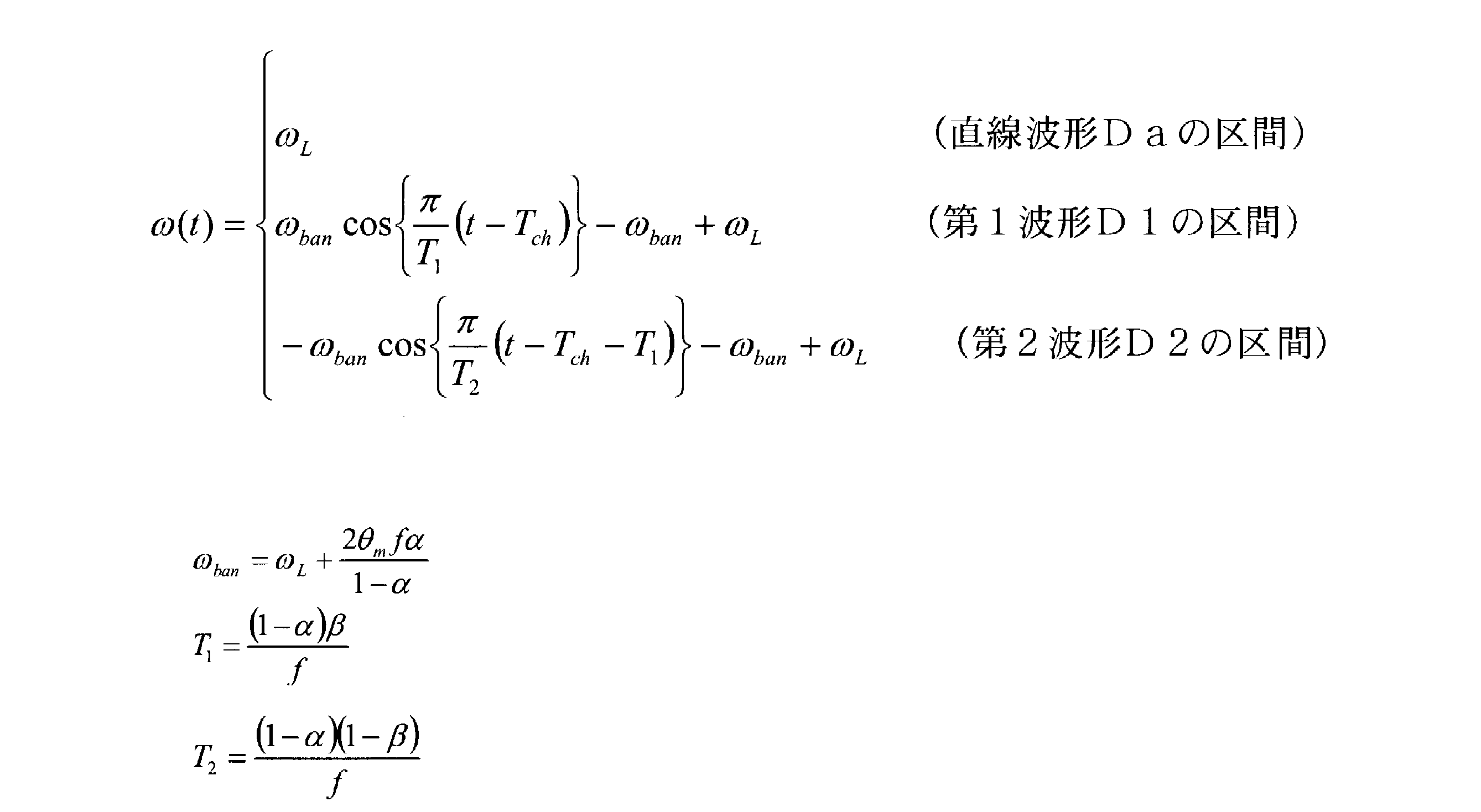
ここで、
ωL:直線波形Daの信号レベルの微分値
Tch:リトレース期間の開始時点の時間
α:鋸波状波形Dのうち直線波形Daの区間の割合(%/100)
β:リトレース波形Dbの区間のうち第1波形D1の区間の割合(%/100)
θm:駆動信号Sbの最大振幅
f:鋸波状波形Dの1周期Tの逆数
である。
ここで、
ωL:直線波形Daの信号レベルの微分値
Tch:リトレース期間の開始時点の時間
α:鋸波状波形Dのうち直線波形Daの区間の割合(%/100)
β:リトレース波形Dbの区間のうち第1波形D1の区間の割合(%/100)
θm:駆動信号Sbの最大振幅
f:鋸波状波形Dの1周期Tの逆数
である。
目標指令生成部21は、この微分値ω(t)の演算により、図11(b)に示す演算結果を得ることができ、この演算結果を積分することによって、図11(a)に示すように直線波形Daとリトレース波形Dbからなる駆動信号Sbを生成する。この駆動信号Sbの信号レベルの微分値ω(t)は、ミラー部10の角速度に比例するものであり、微分値ω(t)の積分値は、ミラー部10の角度の変化量を意味する。従って、光束走査期間において、鋸波状波形Dに重畳する高周波成分を低減することができ、光束走査期間において、駆動信号波形の直線性を向上させることができる。しかも、三角関数を用いた比較的簡単な演算により、駆動信号波形を生成することができるため、駆動信号波形時の演算負荷を小さくすることができる。
[2.画像表示装置]
次に、上述した光走査素子を備えた画像表示装置について説明する。
次に、上述した光走査素子を備えた画像表示装置について説明する。
図12に示すように、本実施形態に係る画像表示装置100は、制御部110、光源部120、走査部140、第2リレー光学系180、ハーフミラー185などを有している。
制御部110は、駆動信号供給部111、主走査駆動信号生成部112、副走査駆動信号生成部113、主制御部114を有している。駆動信号供給部111は、外部から入力された画像信号S(例えば、NTSCコンポジット信号、コンポーネント信号)に基づいて、画像を形成するための要素となる三原色各色のRGB画素信号115r,115g,115bを画素単位で生成する。主走査駆動信号生成部112は、主走査部160の後述する光走査素子161が共振状態で所定走査範囲となるように、主走査部160で使用される主走査駆動信号116を生成して出力する。また、副走査駆動信号生成部113は、主走査駆動信号116の周波数に基づいて、副走査部170で使用される鋸波形状の副走査駆動信号117を生成して出力する。
光源部120には、Rレーザドライバ121,Gレーザドライバ122,Bレーザドライバ123が設けられる。各レーザドライバ121,122,123は、それぞれ駆動信号供給部111から出力されるR,G,B駆動信号115r,115g,115bをもとに、各レーザ124,125,126へそれぞれ駆動電流を供給する。各レーザ124,125,126は、各レーザドライバ121,122,123から供給される駆動電流に応じて強度変調されたレーザ光を出射する。各レーザ124,125,126から出射したR(赤色)レーザ光Lr,G(緑色)レーザ光Lg、B(青色)レーザ光Lbは、コリメート光学系127,128,129によってそれぞれ平行光化された後に、ダイクロイックミラー130,131,132に入射される。その後、これらのダイクロイックミラー130,131,132により、3原色の各レーザ光Lr,Lg,Lbが波長選択的に反射・透過して結合光学系133に達し、合波されて光ファイバケーブル135へ出射される。このように光ファイバケーブル135へ出射されるレーザ光は、強度変調された各色のレーザ光が合波されたものである。
走査部140は、コリメート光学系151、主走査部160、第1リレー光学系165、副走査部170などを有している。
コリメート光学系151は、光源部120で生成され、光ファイバケーブル135を介して出射されるレーザ光を平行光化する。
主走査部160及び副走査部170は、光ファイバケーブル135から入射されたレーザ光を画像として利用者の眼190の網膜190bに投影可能な状態にするために、主走査方向と副走査方向に走査する光学系である。主走査部160は、コリメート光学系151で平行光化されて入射するレーザ光を主走査方向に相対的に高速に往復走査する光走査素子161を有する。また、副走査部170は、主走査部160で主走査方向に走査され、第1リレー光学系165を介して入射するレーザ光を副走査方向に相対的に低速に走査する光走査素子171を有する。この副走査方向は主走査方向に略直交する方向である。例えば、主走査方向を水平方向、副走査方向を垂直方向とすることができる。
主走査部160と副走査部170との間でレーザ光を中継する第1リレー光学系165は、光走査素子161によって主走査方向に走査されたレーザ光を光走査素子171のミラー部に収束させる。そして、このレーザ光が光走査素子171によって副走査方向に走査される。光走査素子171によって走査されたレーザ光は、正の屈折力を持つ2つのレンズ180a,180bが直列配置された第2リレー光学系180を介して、眼190の前方に位置させたハーフミラー185で反射されて利用者の瞳孔190aに入射する。これにより、網膜190b上に画像信号Sに応じた画像が投影され、利用者は瞳孔190aに入射するレーザ光を画像として認識する。また、ハーフミラー185は外光L2を透過して利用者の瞳孔190aに入射させるようにしており、これにより利用者は外光L2に基づく外景にレーザ光L1に基づく画像を重ねた画像を視認することができる。このように画像表示装置100は、画像信号Sに応じた画像と外景とを重ねて利用者の眼190の網膜に結像させる、シースルー型網膜走査型画像表示装置である。
以上のように構成された画像表示装置100において、光走査素子171は、光走査素子4と同様の構成であり、副走査駆動信号生成部113は、上述した光走査装置1の制御部2と同様に、光走査素子171を駆動するようにしている。そのため、光束を走査する期間において、一定の角速度で高精度にミラー部10を駆動することができ、しかも、演算負荷を小さくすることができる。
なお、ここでは、光束の一例として、効率面で有利であるレーザ光を用いているが、光束はレーザ光に限られるものではない。
また、光走査素子のミラー部の角度を検出する検出部を、ピエゾ抵抗素子により構成しているが、圧電素子による検出方法や静電容量の変化による検出方法を用いてもよい。
本発明を、上述してきた実施形態を通して説明したが、本実施形態によれば、両側から梁部11a,11bで支持されたミラー部10を有し、梁部11a,11bの捻れ変位によりミラー部10を揺動可能とした非共振型の光走査素子4(171)と、駆動信号Sb(117)を生成してミラー部10を揺動させる制御部2(110)と、を備え、制御部2(110)は、駆動信号Sb(117)の波形を鋸波状波形Dとし、当該鋸波状波形Dのうち、光束を走査する期間の波形を直線波形Daとする一方、光束を走査しない期間の波形Dbの微分波形が、一つの周波数の1周期の波形、又は、2つの周波数の半周期の波形を互いに結合した波形、となり、かつ、光束を走査しない期間の波形の両端部のそれぞれが、光束を走査する期間の波形の傾きと同じ傾きとなるように光束を走査しない期間の波形を形成し、光束を走査しない期間の波形の両端部のそれぞれを光束を走査する期間の波形の両端部のそれぞれに連続させたので、光束走査期間において、鋸波状波形Dに重畳する高周波成分を低減することができ、駆動信号波形の直線性を向上させることができる。しかも、三角関数を用いた比較的簡単な演算により駆動信号波形を生成することで、駆動信号波形時の演算負荷を小さくすることができる。
また、ミラー部10の変位を検出する検出部18を備え、制御部2(110)は、駆動信号Sb(117)の波形を基にした変位指令と検出部18で検出したミラー部10の変位との誤差分を検出し、その誤差分に基づいて駆動信号Sb(117)を補正するフィードバック制御を行うので、光走査素子4(171)のミラー部10を精度良く揺動することができる。
1 光走査装置
2,110 制御部
4, 161,171 光走査素子
10 ミラー部
10a 反射面
100 画像表示装置
Sb 駆動信号
2,110 制御部
4, 161,171 光走査素子
10 ミラー部
10a 反射面
100 画像表示装置
Sb 駆動信号
Claims (5)
- 両側から梁部で支持されたミラー部を有し、前記梁部の捻れ変位によりミラー部を揺動可能とした非共振型の光走査素子と、駆動信号を生成して前記ミラー部を揺動させる制御部と、を備えた光走査装置において、
前記制御部は、
前記駆動信号の波形を鋸波状波形とし、当該鋸波状波形のうち、光束を走査する期間の波形を直線波形とする一方、光束を走査しない期間の波形の微分波形が、一つの周波数の1周期の波形、又は、2つの周波数の半周期の波形を互いに結合した波形、となり、かつ、当該光束を走査しない期間の波形の両端部のそれぞれが、光束を走査する期間の波形の傾きと同じ傾きとなるように前記光束を走査しない期間の波形を形成し、前記光束を走査しない期間の波形の両端部のそれぞれを前記光束を走査する期間の波形の両端部のそれぞれに連続させた
ことを特徴とする光走査装置。 - 前記光束を走査しない期間の波形を、一つの周波数の1周期の波形により形成しており、
ωLを前記鋸波状波形のうち前記直線波形の微分値とし、Tchを前記鋸波状波形のうち光束を走査しない期間の開始時点の時間とし、αを前記鋸波状波形のうち前記直線波形の区間の割合(%/100)とし、θmを前記駆動信号の最大振幅とし、fを前記鋸波状波形の1周期の逆数としたとき、前記駆動信号の微分値ω(t)は、

を満たすことを特徴とする請求項1に記載の光走査装置。 - 前記光束を走査しない期間の波形を、2つの周波数の半周期の第1波形と第2波形を結合した波形により形成しており、
ωLを前記鋸波状波形のうち前記直線波形の微分値とし、Tchを前記鋸波状波形のうち光束を走査しない期間の開始時点の時間とし、αを前記鋸波状波形のうち前記直線波形の区間の割合(%/100)とし、βを前記第1波形及び第2波形の区間のうち前記第1波形の区間の割合(%/100)とし、θmを前記駆動信号の最大振幅とし、fを前記鋸波状波形の1周期の逆数としたとき、前記駆動信号の微分値ω(t)は、
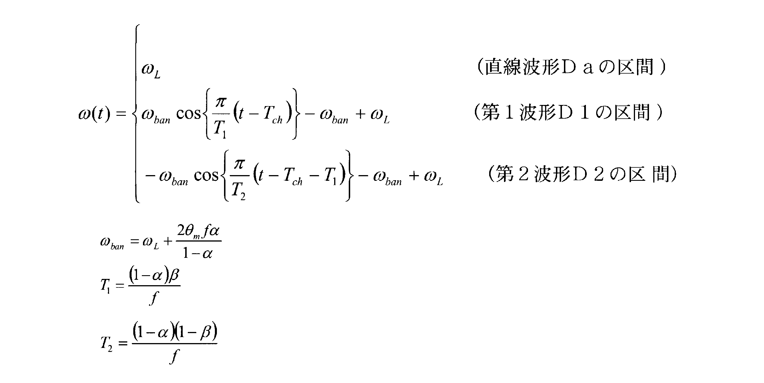
を満たすことを特徴とする請求項1に記載の光走査装置。 - 前記ミラー部の変位を検出する検出部を備え、
前記制御部は、前記駆動信号の波形を基にした変位指令と前記検出部で検出した前記ミラー部の変位との誤差分を検出し、その誤差分に基づいて駆動信号を補正するフィードバック制御を行う
ことを特徴とする請求項1に記載の光走査装置。 - 画像信号に応じた強度の光束を出射する光源と、
前記光源から出射された光束を第1方向に相対的に高速に走査する第1光走査素子と、
両側から梁部で支持されたミラー部を有し、前記梁部の捻れ変位によりミラー部を揺動軸回りに揺動させて前記第1走査素子により走査された光束を前記ミラー部により第1方向と略直交する第2方向に相対的に低速に走査する非共振型の第2光走査素子と、
前記第1及び第2の光走査素子を制御する制御部と、を備えた画像表示装置において、
前記制御部は、
前記第2の光走査素子のミラー部を揺動させる駆動信号の波形を鋸波状波形とし、当該鋸波状波形のうち、光束を走査する期間の波形を直線波形とする一方、光束を走査しない期間の波形の微分波形が、一つの周波数の1周期の波形、又は、2つの周波数の半周期の波形を互いに結合した波形、となり、かつ、当該光束を走査しない期間の波形の両端部のそれぞれが、光束を走査する期間の波形の傾きと同じ傾きとなるように前記光束を走査しない期間の波形を形成し、前記光束を走査しない期間の波形の両端部のそれぞれを前記光束を走査する期間の波形の両端部のそれぞれに連続させた
ことを特徴とする画像表示装置。
Applications Claiming Priority (2)
| Application Number | Priority Date | Filing Date | Title |
|---|---|---|---|
| JP2010-082615 | 2010-03-31 | ||
| JP2010082615A JP2011215324A (ja) | 2010-03-31 | 2010-03-31 | 光走査装置及び画像表示装置 |
Publications (1)
| Publication Number | Publication Date |
|---|---|
| WO2011122410A1 true WO2011122410A1 (ja) | 2011-10-06 |
Family
ID=44712120
Family Applications (1)
| Application Number | Title | Priority Date | Filing Date |
|---|---|---|---|
| PCT/JP2011/056917 Ceased WO2011122410A1 (ja) | 2010-03-31 | 2011-03-23 | 光走査装置及び画像表示装置 |
Country Status (2)
| Country | Link |
|---|---|
| JP (1) | JP2011215324A (ja) |
| WO (1) | WO2011122410A1 (ja) |
Cited By (5)
| Publication number | Priority date | Publication date | Assignee | Title |
|---|---|---|---|---|
| CN107505704A (zh) * | 2017-09-15 | 2017-12-22 | 华中科技大学 | 一种光纤螺旋扫描器的驱动调节方法及装置 |
| CN110297323A (zh) * | 2018-03-22 | 2019-10-01 | 三美电机株式会社 | 促动器以及光扫描装置 |
| CN110389443A (zh) * | 2018-04-18 | 2019-10-29 | 三美电机株式会社 | 扫描驱动装置、光扫描控制装置以及驱动波形生成方法 |
| CN110632753A (zh) * | 2018-06-21 | 2019-12-31 | 华为技术有限公司 | 阶跃驱动信号控制方法和装置 |
| EP2998777B1 (de) * | 2014-09-05 | 2023-02-22 | Fraunhofer-Gesellschaft zur Förderung der angewandten Forschung e.V. | Piezoelektrischer positionssensor für piezoelektrisch angetriebene resonante mikrospiegel |
Families Citing this family (5)
| Publication number | Priority date | Publication date | Assignee | Title |
|---|---|---|---|---|
| JPWO2015125190A1 (ja) * | 2014-02-20 | 2017-03-30 | 株式会社Jvcケンウッド | 画像表示装置および画像表示方法 |
| US9470503B2 (en) | 2014-02-26 | 2016-10-18 | Apple Inc. | Strain-based sensing of mirror position |
| JP7011164B2 (ja) * | 2018-03-15 | 2022-02-10 | ミツミ電機株式会社 | アクチュエータ及び光走査装置 |
| US11004372B2 (en) | 2018-12-11 | 2021-05-11 | Microsoft Technology Licensing, Llc | Controlling a scanning mirror system |
| US11880031B1 (en) | 2020-01-14 | 2024-01-23 | Apple Inc. | Strain-based sensing of dual-axis mirror rotation |
Citations (2)
| Publication number | Priority date | Publication date | Assignee | Title |
|---|---|---|---|---|
| JPH11160434A (ja) * | 1997-11-26 | 1999-06-18 | Mitsubishi Electric Corp | 距離測定装置 |
| JP2006276399A (ja) * | 2005-03-29 | 2006-10-12 | Brother Ind Ltd | 光走査装置、光走査型表示装置及び光走査方法 |
-
2010
- 2010-03-31 JP JP2010082615A patent/JP2011215324A/ja active Pending
-
2011
- 2011-03-23 WO PCT/JP2011/056917 patent/WO2011122410A1/ja not_active Ceased
Patent Citations (2)
| Publication number | Priority date | Publication date | Assignee | Title |
|---|---|---|---|---|
| JPH11160434A (ja) * | 1997-11-26 | 1999-06-18 | Mitsubishi Electric Corp | 距離測定装置 |
| JP2006276399A (ja) * | 2005-03-29 | 2006-10-12 | Brother Ind Ltd | 光走査装置、光走査型表示装置及び光走査方法 |
Cited By (9)
| Publication number | Priority date | Publication date | Assignee | Title |
|---|---|---|---|---|
| EP2998777B1 (de) * | 2014-09-05 | 2023-02-22 | Fraunhofer-Gesellschaft zur Förderung der angewandten Forschung e.V. | Piezoelektrischer positionssensor für piezoelektrisch angetriebene resonante mikrospiegel |
| CN107505704A (zh) * | 2017-09-15 | 2017-12-22 | 华中科技大学 | 一种光纤螺旋扫描器的驱动调节方法及装置 |
| CN107505704B (zh) * | 2017-09-15 | 2019-05-14 | 华中科技大学 | 一种光纤螺旋扫描器的驱动调节方法及装置 |
| CN110297323A (zh) * | 2018-03-22 | 2019-10-01 | 三美电机株式会社 | 促动器以及光扫描装置 |
| CN110297323B (zh) * | 2018-03-22 | 2022-07-01 | 三美电机株式会社 | 促动器以及光扫描装置 |
| CN110389443A (zh) * | 2018-04-18 | 2019-10-29 | 三美电机株式会社 | 扫描驱动装置、光扫描控制装置以及驱动波形生成方法 |
| CN110389443B (zh) * | 2018-04-18 | 2023-08-08 | 三美电机株式会社 | 扫描驱动装置、光扫描控制装置以及驱动波形生成方法 |
| CN110632753A (zh) * | 2018-06-21 | 2019-12-31 | 华为技术有限公司 | 阶跃驱动信号控制方法和装置 |
| CN110632753B (zh) * | 2018-06-21 | 2021-10-01 | 华为技术有限公司 | 阶跃驱动信号控制方法和装置 |
Also Published As
| Publication number | Publication date |
|---|---|
| JP2011215324A (ja) | 2011-10-27 |
Similar Documents
| Publication | Publication Date | Title |
|---|---|---|
| JP2011215324A (ja) | 光走査装置及び画像表示装置 | |
| JP5176823B2 (ja) | 光走査装置、画像表示装置及び光走査装置の駆動方法 | |
| JP5524535B2 (ja) | アクチュエータの駆動装置 | |
| US9251730B2 (en) | Image display apparatus and image scanning apparatus | |
| WO2005093491A1 (ja) | 光走査装置およびそれを備えた画像形成装置 | |
| US10187620B2 (en) | Display device | |
| US7884986B2 (en) | Optical scanning device, optical scanning display device, and optical scanning method | |
| CN104204900A (zh) | 扫描反射镜以及扫描型图像显示装置 | |
| WO2007122974A1 (ja) | 光走査装置及び画像表示装置並びに網膜走査型画像表示装置 | |
| JP5098759B2 (ja) | 画像投影装置 | |
| JP2010237536A (ja) | 画像表示装置 | |
| JP4779534B2 (ja) | 光走査型ディスプレイ | |
| JP2011215398A (ja) | 画像表示装置 | |
| EP2646868A1 (en) | A method for projecting an image | |
| JP2011180277A (ja) | 画像表示装置 | |
| JP4929738B2 (ja) | 光走査装置、光走査装置の制御方法及び画像表示装置 | |
| CN111610627B (zh) | 光扫描装置及其控制方法 | |
| JP2012003051A (ja) | 走査型画像表示装置 | |
| WO2011125494A1 (ja) | 光走査装置及び画像表示装置 | |
| JP5152075B2 (ja) | 駆動信号発生器及びそれを備えた光走査装置並びに画像表示装置 | |
| JP2020106741A (ja) | 光走査装置及びその制御方法 | |
| JP2011215325A (ja) | 光走査装置及び画像表示装置 | |
| JP2011075948A (ja) | 画像表示装置 | |
| WO2011108395A1 (ja) | 光走査装置及びそれを備えた画像表示装置 | |
| JP2010256862A (ja) | ミラーデバイス駆動制御装置およびプロジェクター |
Legal Events
| Date | Code | Title | Description |
|---|---|---|---|
| 121 | Ep: the epo has been informed by wipo that ep was designated in this application |
Ref document number: 11762642 Country of ref document: EP Kind code of ref document: A1 |
|
| NENP | Non-entry into the national phase |
Ref country code: DE |
|
| 122 | Ep: pct application non-entry in european phase |
Ref document number: 11762642 Country of ref document: EP Kind code of ref document: A1 |