WO2011121980A1 - 固体電解コンデンサ - Google Patents
固体電解コンデンサ Download PDFInfo
- Publication number
- WO2011121980A1 WO2011121980A1 PCT/JP2011/001830 JP2011001830W WO2011121980A1 WO 2011121980 A1 WO2011121980 A1 WO 2011121980A1 JP 2011001830 W JP2011001830 W JP 2011001830W WO 2011121980 A1 WO2011121980 A1 WO 2011121980A1
- Authority
- WO
- WIPO (PCT)
- Prior art keywords
- anode
- capacitor element
- cathode
- terminal plate
- electrode portion
- Prior art date
- Legal status (The legal status is an assumption and is not a legal conclusion. Google has not performed a legal analysis and makes no representation as to the accuracy of the status listed.)
- Ceased
Links
Images



Classifications
-
- H—ELECTRICITY
- H01—ELECTRIC ELEMENTS
- H01G—CAPACITORS; CAPACITORS, RECTIFIERS, DETECTORS, SWITCHING DEVICES, LIGHT-SENSITIVE OR TEMPERATURE-SENSITIVE DEVICES OF THE ELECTROLYTIC TYPE
- H01G9/00—Electrolytic capacitors, rectifiers, detectors, switching devices, light-sensitive or temperature-sensitive devices; Processes of their manufacture
- H01G9/15—Solid electrolytic capacitors
-
- H—ELECTRICITY
- H01—ELECTRIC ELEMENTS
- H01G—CAPACITORS; CAPACITORS, RECTIFIERS, DETECTORS, SWITCHING DEVICES, LIGHT-SENSITIVE OR TEMPERATURE-SENSITIVE DEVICES OF THE ELECTROLYTIC TYPE
- H01G9/00—Electrolytic capacitors, rectifiers, detectors, switching devices, light-sensitive or temperature-sensitive devices; Processes of their manufacture
- H01G9/004—Details
- H01G9/008—Terminals
- H01G9/012—Terminals specially adapted for solid capacitors
-
- H—ELECTRICITY
- H01—ELECTRIC ELEMENTS
- H01G—CAPACITORS; CAPACITORS, RECTIFIERS, DETECTORS, SWITCHING DEVICES, LIGHT-SENSITIVE OR TEMPERATURE-SENSITIVE DEVICES OF THE ELECTROLYTIC TYPE
- H01G9/00—Electrolytic capacitors, rectifiers, detectors, switching devices, light-sensitive or temperature-sensitive devices; Processes of their manufacture
- H01G9/004—Details
- H01G9/04—Electrodes or formation of dielectric layers thereon
- H01G9/048—Electrodes or formation of dielectric layers thereon characterised by their structure
-
- Y—GENERAL TAGGING OF NEW TECHNOLOGICAL DEVELOPMENTS; GENERAL TAGGING OF CROSS-SECTIONAL TECHNOLOGIES SPANNING OVER SEVERAL SECTIONS OF THE IPC; TECHNICAL SUBJECTS COVERED BY FORMER USPC CROSS-REFERENCE ART COLLECTIONS [XRACs] AND DIGESTS
- Y02—TECHNOLOGIES OR APPLICATIONS FOR MITIGATION OR ADAPTATION AGAINST CLIMATE CHANGE
- Y02T—CLIMATE CHANGE MITIGATION TECHNOLOGIES RELATED TO TRANSPORTATION
- Y02T10/00—Road transport of goods or passengers
- Y02T10/60—Other road transportation technologies with climate change mitigation effect
- Y02T10/70—Energy storage systems for electromobility, e.g. batteries
Definitions
- the present invention relates to a solid electrolytic capacitor in which a thin metal terminal plate and a capacitor element are combined, and more particularly to a solid electrolytic capacitor in which peeling of the terminal plate from the capacitor element is suppressed.
- Patent Documents 1 to 4 disclose a structure in which a capacitor element and a substrate are combined to reduce the distance from the capacitance forming portion of the solid electrolytic capacitor to the LSI. These solid electrolytic capacitors are configured to supply power from electrodes formed on a substrate.
- the applicant has proposed Japanese Patent Application No. 2009-88320 and International Patent Application PCT / JP2009 / 04035 as novel solid electrolytic capacitors combining a capacitor element and a substrate.
- the capacitor element has a dielectric oxide film layer formed on the inner surface of the concave portion provided in the center of the anode body, and the solid electrolyte layer (as the polymerizable monomer, thiophene, The use of pyrrole or other derivatives is preferred) and a power outlet is formed outside the capacitor element via the cathode portion.
- the capacitor element draws out the cathode electrode to the outside of the solid electrolytic capacitor through the mounting substrate, and the anode around the central portion of the capacitor element is drawn out through the anode portion and the conductor of the mounting substrate. .
- both the anode and the cathode can shorten the current path inside the solid electrolytic capacitor.
- the solid electrolytic capacitor of the international patent application PCT / JP2009 / 04035 includes the following terminal plate as a substrate to be combined with the capacitor element. That is, on the terminal plate, an anode electrode portion and a cathode electrode portion made of a thin metal plate are arranged on the same plane with a gap therebetween. An insulating resin is interposed in the gap between the anode electrode portion and the cathode electrode portion, the anode electrode portion and the cathode electrode portion are electrically insulated by the insulating resin, and both electrode portions are integrated into a sheet shape. .
- Such a terminal plate is superimposed on the connection surface of the capacitor element, and the anode electrode portion of the terminal plate is electrically connected to the anode lead portion of the capacitor element, and the cathode electrode of the terminal plate is electrically connected to the cathode lead portion of the capacitor element.
- the distance from the anode lead portion and the cathode lead portion of the capacitor element to the anode electrode portion and the cathode electrode portion of the terminal plate, which is the current outlet is achieved only by the distance of the thickness of the terminal plate. This is possible, and the current path can be shortened.
- the solid electrolytic capacitor is a normal resin-molded solid electrolytic capacitor or a solid electrolytic capacitor having a substrate in which the front and back of the resin plate are connected by through-hole electrodes, the gas pressure is solid electrolytic. There was no risk of adversely affecting the capacitor.
- a solid electrolytic capacitor in which a capacitor element is mounted on a substrate and the through-hole electrode of the substrate and the anode part and the cathode part of the capacitor element are respectively joined by a conductive adhesive has a high mechanical strength of the board itself, If the adhesion between the resin substrate and the mold resin is good, the gas pressure is relieved by the flexibility of the resin.
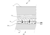
- FIG. 8 is an enlarged cross-sectional view in a state where the capacitor element 10 is mounted on the terminal plate 20, and shows a state where the capacitor element 10 and the terminal plate 20 are joined by the conductive adhesive 30.
- a cathode lead portion 14 including a polymer layer and a graphite layer is formed on one surface of the anode body 11, and the cathode lead portion 14 is the anode body 11 (metal such as aluminum). Facing.
- the side on which the solid electrolyte layer is formed serves as an outlet for gasified unpolymerized monomer and residual solvent. For this reason, a gas pressure is applied to the terminal board 20 by the gas (it shows with the arrow in FIG. 8) discharge
- the terminal plate 20 is a thin metal plate, its elasticity is poor as a material, and it is not possible to expect a gas pressure relaxation effect like a resin.
- the bonding surface side of the conductive adhesive 30 with respect to the terminal board 20 was deformed, and the conductive adhesive 30 was peeled off from the terminal board 20.
- the cathode electrode portion 22 of the terminal plate 20 occupies a large area of the metal foil, and the metal plate is extremely thin, so that a large deformation is likely to occur when a gas pressure is applied. Therefore, the peeling between the conductive adhesive 30 and the terminal board 20 was remarkable.
- the current path is shortened as much as possible to improve the transient response, but it is exposed to high heat during solder reflow.
- the terminal plate 20 made of a thin metal plate is deformed and the conductive adhesive 30 is peeled off from the terminal plate 20, resulting in deterioration of ESR characteristics and further ESL characteristics. .
- the present invention has been proposed in order to solve the above-described problems.
- the current path is short and the transient response is good.
- the capacitor element and the terminal plate made of a thin metal are connected with a conductive adhesive.
- An object of the present invention is to provide a solid electrolytic capacitor that prevents the peeling of an adhesive material and suppresses an increase in ESR characteristics even when bonded.
- the present invention comprises a capacitor element and a terminal plate, and the capacitor element is provided with a cathode part and an anode part on at least one side of an anode body made of a valve metal, and the cathode part is provided with a dielectric.
- An oxide film layer, a solid electrolyte layer, and a cathode lead portion are sequentially formed, and the anode lead portion is led out from the anode portion of the anode body, and the terminal plate is an anode electrode portion and a cathode electrode made of a thin metal plate Are disposed on the same plane with a gap therebetween, and an insulating resin is interposed in the gap between the anode electrode portion and the cathode electrode portion, and the anode electrode portion and the cathode electrode portion are electrically connected by the insulating resin.
- the anode electrode of the terminal plate is connected to the anode lead portion of the capacitor element.
- the cathode electrode part of the terminal plate is electrically connected to the cathode lead part of the capacitor element, respectively, the anode lead part and the anode electrode part, and the cathode lead part and the cathode electrode part Are electrically connected by a conductive adhesive, and the gap between the capacitor element and the terminal plate is filled with an insulating resin.
- the resin since the gap between the electrode lead portion of the capacitor element and the electrode portion of the terminal plate is filled with the insulating resin, the resin enters between the conductive adhesives, and the resin is transferred to the electrode portion. In close contact. Resin has better adhesion to the metal that constitutes the terminal board than conductive adhesive, so even if gas is generated from the capacitor element due to high heat during solder reflow, the gas pressure adheres to the electrode part. The received resin can be received, the terminal plate is not deformed, and the conductive adhesive is not peeled off from the electrode portion, so that an increase in ESR characteristics can be suppressed.
- FIG. 4 is a partially enlarged view of FIG. 3. The partial top view of the capacitor
- Configuration of the present embodiment (1-1) Configuration of the capacitor element 10
- the capacitor element 10 used in the present embodiment has a substantially rectangular aluminum shape with a thickness of about 100 to 500 ⁇ m as shown in FIG. Or a valve metal foil (hereinafter referred to as anode body 11).
- the central portion of the anode body 11 is enlarged by etching to form a porous etching layer 12 on one surface of the anode body 11 (FIG. 1-b).
- a dielectric oxide film serving as a dielectric layer is formed on the etching layer 12, and a cathode lead portion 14 composed of a solid electrolyte layer, a graphite layer, and a silver paste layer is sequentially formed (FIG. 1-c).
- the solid electrolyte layer formed on the dielectric oxide film is formed by sequentially immersing the anode body 11 in the polymerizable monomer solution and the oxidizing agent solution, and pulling up from each solution to advance the polymerization reaction.
- the solid electrolyte layer may be formed by a method of applying or discharging a polymerizable monomer solution and an oxidant solution. Moreover, the method of immersing or apply
- the solid electrolyte layer can also be formed by electrolytic polymerization used in the field of solid electrolytic capacitors, or by applying and drying a conductive polymer solution.
- a solid electrolyte layer can be formed by combining these solid electrolyte formation methods.
- the polymerizable monomer used for forming the solid electrolyte layer thiophene, pyrrole or their derivatives can be preferably used.
- a separation layer 15 is formed on the capacitor element 10 to divide the anode lead portion 13 and the cathode lead portion 14 of the capacitor element 10. After the etching process is completed, the separation layer 15 is coated with an insulating resin and penetrated into the etching layer 12 to insulate the anode lead portion 13 and the etching layer 12.
- the anode lead portion 13 and the cathode lead portion 14 of the capacitor element 10 are preferably on the same plane.
- a metal piece 16 such as aluminum can be bonded to the surface of the anode lead portion 13 for the purpose of adjusting the height of the anode lead portion 13 and the cathode lead portion 14.
- the terminal board 20 in the present embodiment is made of a thin copper plate (copper foil or copper alloy foil) as an example, and the capacitor element 10
- the metal plate constituting the anode electrode portion 21 and the metal plate constituting the cathode electrode portion 22 are insulated by the insulating resin 23.
- the mounting land has substantially the same mounting land as the anode lead portion 13 and the cathode lead portion 14. It is.
- the internal structure of the terminal plate 20 is such that the front and back of a metal plate made of a single copper plate are electrically connected, and the gap between the anode electrode portion 21 and the cathode electrode portion 22 is electrically connected.
- Insulating resin 23 enters the part to insulate it, and integration is achieved by covering part of the surface of the copper plate continuously with the resin in the gap.
- the anode electrode portion 21 made of a thin metal plate and the cathode electrode portion 22 also made of a thin metal plate are arranged on the same plane with a predetermined width gap, and an insulating property is provided in the gap portion between the two.
- a resin 23 is interposed, the anode electrode portion 21 and the cathode electrode portion 22 are electrically insulated by the insulating resin 23, and both electrodes are integrated into a sheet shape.
- the metal plate constituting the terminal plate 20 it is preferable to use a rolled copper foil having a thickness of 15 ⁇ m to 100 ⁇ m.
- the insulating resin 23 has a thickness that protrudes at a predetermined height on both sides of the metal plate constituting the terminal plate 20 so that the anode electrode portion 21 and the cathode electrode portion 22 are integrated reliably. This is desirable.
- the same thickness as that of the metal plate, or the joint portion with the metal plate may be a drum-shaped cross section having a thicker thickness than the metal plate and a thinner central portion.
- a polyester resin or a polyimide resin is used, but is not necessarily limited thereto. Other resins can be used as long as the insulating properties, adhesion to the metal plate, strength, and the like are compatible with the solid electrolytic capacitor to be used.
- the copper plate to be the anode electrode portion 21 and the copper plate to be the cathode electrode portion 22 of the terminal plate 20 are arranged at predetermined positions in a state where they are separated from each other.
- Insulating resin 23 is applied to a predetermined position including a gap portion between the copper plate serving as the anode electrode portion 21 and the copper plate serving as the cathode electrode portion 22 of the terminal plate 20 and thermally cured.
- the insulating resin 23 is applied to the gap between the anode electrode portion 21 and the cathode electrode portion 22 of the copper plate and the periphery of the gap portion, and the thickness of the insulating resin 23 is larger than that of the copper plate. Both are preferably applied so as to protrude with a thickness of a predetermined height. Further, the shape of the exposed portion (mounting land) of the copper plate is made to match the anode lead portion 13 and the cathode lead portion 14 of the capacitor element 10.
- the width of the gap portion can be arbitrarily set according to required characteristics. Specifically, the width of the gap can be made close to about 20 ⁇ m.
- the solid electrolytic capacitor of this embodiment has the capacitor element 10 mounted on a terminal board 20.
- a conductive adhesive 30 such as a silver paste.
- the silver paste is applied to the capacitor element 10 or the terminal plate 20 for adhesion, but at this time, the silver paste may flow to cause a short circuit between the anode and the cathode.
- the terminal board 20 is formed so that the thickness of the insulating resin layer 23 protrudes at a predetermined height on both sides of the copper board. For this reason, the protrusion part of the insulating resin layer 23 comes to dampen the flow of the silver paste, and a short circuit between the anode electrode part 21 and the cathode electrode part 22 can be prevented.
- the height of the protrusion part of the insulating resin 23 is arbitrary, if the protrusion height is high, the effect of blocking the silver paste when the capacitor element 10 is mounted becomes high.
- the gap between the anode electrode portion 21 and the cathode electrode portion 22 is insulated by the insulating resin 23, and the insulating resin 23 is also formed around the gap portion, thereby joining the anode and the cathode.
- Strength is increased.
- the mechanical strength of the terminal plate 20 is improved, and the distance between the anode electrode portion 21 and the cathode electrode portion 22 on the surface on which the capacitor element is mounted can be increased.
- the anode electrode portion 21 and the cathode electrode portion 22 can be more reliably insulated.
- the structural features of the present embodiment are that the anode lead portion 13 and the cathode lead portion 14 of the capacitor element 10 and the terminal plate 20
- the gap between the electrode portions 21 and 22 is filled with an insulating resin 31 such as an epoxy resin. More specifically, when the capacitor element 10 and the terminal plate 20 are bonded and thermally cured, the distance between the capacitor element 10 and the terminal plate 20 is about 20 ⁇ m, and this gap is filled with the insulating resin 31.
- the conductive adhesive 30 is applied to the cathode lead portion 14 of the capacitor element 10 in a dot shape at intervals of about 300 ⁇ m so as to have a diameter of about 300 ⁇ m (5 ⁇ 5 in the example shown in FIG. 5). Place).
- the cathode of the terminal plate from the cathode lead portion of the capacitor element is compared with the case where the capacitor element 10 is attached to the lead frame and resin molded.
- the distance to the electrode part can be made extremely short.
- the terminal plate 20 is a single copper plate whose front and back are integrated, and has more conductive paths than a flexible substrate that is connected through the through hole. Therefore, the electrical resistance between the front and back of the terminal board 20 is small, and the internal resistance of the solid electrolytic capacitor can be reduced.
- the high frequency component of the current is the peripheral edges of the anode electrode portion 21 and the cathode electrode portion 22 of the terminal plate 20.
- the terminal board 20 of the present embodiment has a structure in which the anode electrode portion 21 and the cathode electrode portion 22 are close to each other with a predetermined interval, and particularly in the high frequency region, the anode electrode portion 21 and the cathode electrode portion 22 are close to each other. The effect of canceling the induced magnetic field is large, and the ESL of the solid electrolytic capacitor can be reduced.
- the width of the gap between the anode electrode portion 21 and the cathode electrode portion 22 of the terminal plate 20 can be arbitrarily set according to the required characteristics. In order to obtain the ESL reduction effect of the solid electrolytic capacitor The width of the gap is preferably set in the range of 20 to 200 ⁇ m.
- the bonding strength between the anode electrode portion 21 and the cathode electrode portion 22 is increased, and the machine of the terminal plate 20 is increased.
- the mechanical strength is improved.
- the insulating resin 23 By disposing the insulating resin 23 in the gap portion of the terminal plate 10, the distance between the anode electrode portion 21 and the cathode electrode portion 22 can be increased on the surface on which the capacitor element 10 is mounted.
- the conductive adhesive 30 is applied in the form of dots, a plurality of conductive paths can be formed, contributing to good transient response characteristics.
- the anode electrode portion 21 and the cathode electrode portion 22 are spaced apart from each other, but due to the skin effect when the high-frequency current flows through the conductor, the high-frequency current is generated between the anode electrode portion 21 and the cathode electrode portion 22 of the terminal plate 10. Since the current flows through the peripheral edge, the current paths themselves are close to each other. Therefore, in this embodiment, the ESL reduction effect is not reduced.
- this embodiment has the following advantages. That is, the capacitor element 10 and the electrode portions 21 and 22 of the terminal plate 20 are joined by the conductive adhesive 30, and the gap between the capacitor element 10 and the terminal plate 20 is filled with the insulating resin 31. For this reason, the insulating resin 31 enters between the conductive adhesives 30. The insulating resin 31 has higher adhesion to the electrode portions 21 and 22 of the terminal plate 20 than the conductive adhesive 30 and can firmly adhere the capacitor element 10 and the terminal plate 20.
- the insulating resin 31 is filled around the conductive adhesive 30 applied in the form of dots, the gas pressure can be dispersed and received. Therefore, it is possible to sufficiently relax the gas pressure. As a result, the terminal plate 20 is not likely to be deformed even when a gas pressure is applied, and the peeling of the conductive adhesive 30 from the electrode portions 21 and 22 can be avoided.
- the ESL can be reduced by shortening the current path as much as possible, and at the same time, the separation between the capacitor element 10 and the terminal plate 20 can be avoided. Is also feasible. Thereby, it is possible to provide a solid electrolytic capacitor having excellent transient response and low impedance up to a high frequency region.
- the present invention is not limited to the above-described embodiments, and the filling amount and filling position of the insulating resin, the dimensions and shapes of the constituent members, and the like can be appropriately determined.
- the formation position of the cathode lead portion 14 of the capacitor element 10 is not limited to the center of the anode body 11 and can be changed as appropriate.
- the application shape of the conductive adhesive 30 can be appropriately selected in addition to the dot shape shown in FIG. Specifically, as shown in FIG. 7, the adhesion area can be increased by applying the conductive adhesive 32 in a star shape.
- the cathode lead portion 14 and the cathode electrode portion 22 are connected by the conductive adhesive 30, and the insulating adhesive 31 is connected between the cathode lead portion 14 and the cathode electrode portion 22.
- Any coating shape that forms a gap that can be filled is acceptable. The same applies to the anode lead portion 13 and the anode electrode portion 21.
- a recess is formed in advance in the anode body 11 as a starting material, and an etching layer, a dielectric oxide film, and a solid electrolyte layer are formed inside the recess. It is also possible to adjust the height by forming a graphite layer and a silver paste layer.
- the cathode lead portion 14 including the solid electrolyte layer or the like is formed in the concave portion of the anode body 11, the solid electrolyte layer is surrounded by the concave portion of the anode body 11 made of a metal material.
- the monomer or residual solvent is strongly released toward the opening side of the recess. Even in such a case, peeling of the conductive adhesive 30 is reliably suppressed by filling the insulating resin 31. Therefore, peeling between the capacitor element 10 and the terminal plate 20 can be surely prevented, the electrical resistance inside the solid electrolytic capacitor is not increased, and an increase in ESR characteristics can be suppressed.
- the cathode lead portion 14 is formed in the concave portion of the anode body 11, whereby the cathode electrode portion 22 can be drawn out of the solid electrolytic capacitor via the terminal plate 20.
- the distance from the dielectric oxide film layer of the capacitor element 10 to the external terminal of the solid electrolytic capacitor can be made extremely short.
- the anode body 11 of the capacitor element 10 can be drawn out as the anode electrode portion 21 through the anode portion and the conductor of the terminal plate 20 as the anode portion around the recess. Therefore, both the anode and the cathode have a very short conductive path inside the solid electrolytic capacitor, and the ESL of the solid electrolytic capacitor can be reduced.
Landscapes
- Engineering & Computer Science (AREA)
- Power Engineering (AREA)
- Microelectronics & Electronic Packaging (AREA)
- Fixed Capacitors And Capacitor Manufacturing Machines (AREA)
- Structures For Mounting Electric Components On Printed Circuit Boards (AREA)
Abstract
電流経路が短く過渡応答性が良好であると同時に、コンデンサ素子と薄い金属からなる端子板を導電性接着材にて接合する場合でも、接着材の剥離を防いでESL特性の上昇を抑えた固体電解コンデンサを提供する。陽極引出部13および陰極引出部14に導電性接着材30が塗布され、コンデンサ素子10が端子板20の陽極電極部21および陰極電極部22に接着されている。また、コンデンサ素子10の陽極引出部13および陰極引出部14と、端子板20の電極部21、22との間隙に、エポキシ樹脂などの絶縁樹脂31が充填されている。
Description
本発明は、薄い金属の端子板とコンデンサ素子とを組み合わせた固体電解コンデンサに係り、特に、コンデンサ素子からの端子板の剥離を抑えた固体電解コンデンサに関するものである。
近年、パーソナルコンピュータや通信関連機器は勿論のこと、家庭電化製品や車載用機器なども、情報電子機器としての機能を備えている。このため、様々な電子機器でLSI等のデジタル回路技術が広く用いられている。このようなデジタル回路技術の普及に伴い、充分な速さで電荷供給ができるように過渡応答性に優れ、高周波領域までインピーダンスの低い固体電解コンデンサが望まれている。これは、LSIを動作させるにあたり、大電流・低電圧で動作するLSIの電源電圧安定化に対応するためである。
固体電解コンデンサにおいて過渡応答特性を良好とするためには、LSI等への供給電圧が低下した際に、固体電解コンデンサから大電力を供給することが要求される。したがって、固体電解コンデンサの特性としては、高周波化に対応するためのESR(等価直列抵抗)が低いことはもとより、ESL(等価直列インダクタンス)が低いことが重視される。
固体電解コンデンサにて低ESL化を図るためには、電流経路を極力短くすることが有効である。例えば、特許文献1~4記載の技術では、コンデンサ素子と基板を組み合わせ、固体電解コンデンサの容量形成部からLSIまでの距離を近くした構造が開示されている。これらの固体電解コンデンサでは、基板に形成した電極から電力の供給を行う構成としている。
また、出願人は、コンデンサ素子と基板を組み合わせた新規な固体電解コンデンサとして、特願2009-88320や国際特許出願PCT/JP2009/04035を提案している。このうち、特願2009-88320の固体電解コンデンサにおいて、コンデンサ素子は、陽極体の中央に設けた凹部の内面に誘電体酸化皮膜層を形成し、固体電解質層(重合性モノマーとしては、チオフェン、ピロールまたはその他の誘導体の使用が好適である)および陰極部を介してコンデンサ素子の外部に電力の引き出し口を形成する。
さらに、コンデンサ素子は、搭載基板を介して固体電解コンデンサの外部に陰極電極を引き出すと共に、コンデンサ素子の中央部分の周囲を陽極部とし、この陽極部および搭載基板の導体を介して陽極電極を引き出す。このような固体電解コンデンサによれば、陽極、陰極とも固体電解コンデンサ内部での電流経路を短くすることができる。
また、国際特許出願PCT/JP2009/04035の固体電解コンデンサでは、コンデンサ素子と組み合わせる基板として、次のような端子板を備えている。すなわち、端子板には、薄い金属板からなる陽極電極部および陰極電極部を同一平面上に間隙を保って配置する。これら陽極電極部と陰極電極部の間隙部には絶縁性樹脂を介在させ、絶縁性樹脂により陽極電極部と陰極電極部とを電気的に絶縁すると共に両電極部をシート状に一体化している。
このような端子板をコンデンサ素子の接続面に重ね合わせ、コンデンサ素子の陽極引き出し部に端子板の陽極電極部を、コンデンサ素子の陰極引出部に端子板の陰極電極を、それぞれ電気的に接続する。このような技術によれば、コンデンサ素子の陽極引出部および陰極引出部から、電流の出口である端子板の陽極電極部および陰極電極部までの距離が、端子板の厚さの距離だけで達成可能であり、電流経路の短縮化を図ることができる。
上述した特願2009-88320あるいは国際特許出願PCT/JP2009/04035に開示された技術では、いずれも、固体電解コンデンサの容量形成部から、電力の引き出し口としての電極までの距離が極めて短くなり、また、固体電解コンデンサの薄型化を進めることができる。したがって、電流経路の短縮化を図って低ESL化を進めることができ、過応答特性の良好な固体電解コンデンサが実現可能となる。
ところで、固体電解コンデンサではプリント基板等に実装する際、半田リフロー法を用いるのが一般的である。しかしながら、半田リフロー工程で固体電解コンデンサを高熱(240~260℃程度)にさらすと、コンデンサ素子からガスが発生することがある。これは、コンデンサ素子の陰極引出部において、固体電解質層には未重合モノマーが、グラファイト層や銀ペースト層には溶媒が、それぞれ残留しているので、高熱により未重合モノマーや残留溶媒がガス化するためである。
このようにコンデンサ素子からガスが発生したとしても、通常の樹脂モールドされた固体電解コンデンサ、あるいは樹脂板の表裏をスルーホール電極で連絡した基板を持つ固体電解コンデンサであれば、ガス圧力が固体電解コンデンサに悪影響を与えるおそれはなかった。
つまり、全体がモールド樹脂で被覆された固体電解コンデンサであれば、コンデンサ素子から発生するガス圧力は、モールド樹脂の柔軟性によって緩和される。また、コンデンサ素子を基板に搭載し、基板のスルーホール電極とコンデンサ素子の陽極部、陰極部をそれぞれ導電性接着材で接合した固体電解コンデンサであれば、基板自体の機械的強度が強く、さらには樹脂基板とモールド樹脂の密着性が良好であれば、樹脂の柔軟性によってガスの圧力が緩和される。
しかしながら、コンデンサ素子と端子板とを導電性接着材にて接合した場合、固体電解コンデンサにおいて陰極引出部からガスが発生することで、ESR特性が悪化することが判明した。この原因について出願人が究明したところ、次のような結論を得た。すなわち、半田リフロー工程で固体電解コンデンサが高熱にさらされたことで、この導電性接着材が端子板から剥離することが確認された。その結果、固体電解コンデンサの内部での電気的抵抗が増加し、ESRの上昇を招いていた。
ここで、半田リフロー工程で導電性接着材と端子板の電極部分が剥離する現象に関し、推定されるメカニズムについて、図8を参照して説明する。図8はコンデンサ素子10を端子板20に実装した状態における拡大断面図であって、コンデンサ素子10と端子板20とを導電性接着材30にて接合した状態を示している。
図8に示すように、コンデンサ素子10では、ポリマー層、グラファイト層を含む陰極引出部14を陽極体11の片面に形成しており、この陰極引出部14は陽極体11(アルミニウム等の金属)に面している。このような陽極体11において、固体電解質層が形成された側が、ガス化した未重合モノマーや、残留溶媒の出口となる。このため、固体電解質層から放出されるガス(図8では矢印で図示)によって、端子板20に気体圧力が加わることになる。
このとき、端子板20は薄い金属板なので、素材として弾性が乏しく、樹脂のような気体圧力の緩和効果を期待することができない。その結果、端子板20に対する導電性接着材30の接着面側が変形し、端子板20から導電性接着材30が剥離した。特に、端子板20のうち、陰極電極部22は金属箔の占有面積が大きく、かつ金属板は極めて薄いため、気体圧力が加わると大きな変形が発生し易い。したがって、導電性接着材30と端子板20との剥離が顕著となっていた。
以上述べたように、コンデンサ素子10と端子板20とを導電性接着材30により接合した固体電解コンデンサでは、電流経路を極力短くして過渡応答性が良好となる反面、半田リフロー時に高熱にさらされてコンデンサ素子10から気体が発生すると、薄い金属板からなる端子板20が変形して導電性接着材30が端子板20から剥がれてしまい、ESR特性やさらにはESL特性の悪化を招いていた。
本発明は、上記の問題点を解消するために提案されたものであり、電流経路が短く過渡応答性が良好であると同時に、コンデンサ素子と薄い金属からなる端子板を導電性接着材にて接合する場合でも、接着材の剥離を防いでESR特性の上昇を抑えた固体電解コンデンサを提供することを目的とするものである。
上記目的を達成するために、本発明は、コンデンサ素子および端子板を備え、コンデンサ素子は、弁作用金属からなる陽極体の少なくとも片面に陰極部および陽極部を設け、前記陰極部には誘電体酸化皮膜層、固体電解質層、陰極引出部を順次形成して、前記陽極体の陽極部から陽極引出部を導出して構成し、前記端子板は、薄い金属板からなる陽極電極部および陰極電極部を同一平面上に間隙を保って配置し、前記陽極電極部と前記陰極電極部の間隙部に絶縁性樹脂を介在させ、この絶縁性樹脂により前記陽極電極部と前記陰極電極部とを電気的に絶縁すると共に両電極部をシート状に一体化して構成し、前記コンデンサ素子の接続面に前記端子板を重ね合わせた状態で、前記コンデンサ素子の陽極引出部に前記端子板の前記陽極電極部を、前記コンデンサ素子の陰極引出部に前記端子板の前記陰極電極部を、それぞれ電気的に接続した固体電解コンデンサにおいて、前記陽極引出部と前記陽極電極部、並びに前記陰極引出部と前記陰極電極部を、それぞれ導電性接着材によって電気的に接続すると共に、前記コンデンサ素子と前記端子板の間隙を絶縁樹脂で充填したことを特徴とするものである。
本発明の固体電解コンデンサによれば、コンデンサ素子の電極引出部と端子板の電極部の間隙を絶縁樹脂にて充填したことで、導電性接着材の間に樹脂が入り込み、電極部に樹脂が密着する。樹脂は導電性接着材に比べ、端子板を構成する金属との密着性が良好であるため、半田リフロー時に高熱にさらされてコンデンサ素子から気体が発生しても、気体圧力を電極部に密着した樹脂が受け止めることができ、端子板が変形して電極部から導電性接着材が剥離することがなく、ESR特性の上昇を抑えることができる。
以下、本発明に係る固体電解コンデンサの代表的な実施形態の一例について、図1~図6を参照して具体的に説明する。なお、図8に示した従来例と同一の部材については同一の符号を付している。
(1)本実施形態の構成
(1-1)コンデンサ素子10の構成
本実施形態で用いるコンデンサ素子10は、図1-aに示すような、厚さが100~500μm程度の略長方形状のアルミニウム等の弁金属板または弁金属箔(以下、陽極体11という)から形成される。この陽極体11の中央部をエッチング処理により拡面化処理し、陽極体11の片面に多孔質のエッチング層12を形成する(図1-b)。
(1-1)コンデンサ素子10の構成
本実施形態で用いるコンデンサ素子10は、図1-aに示すような、厚さが100~500μm程度の略長方形状のアルミニウム等の弁金属板または弁金属箔(以下、陽極体11という)から形成される。この陽極体11の中央部をエッチング処理により拡面化処理し、陽極体11の片面に多孔質のエッチング層12を形成する(図1-b)。
陽極体11の両端部の未エッチング部は、コンデンサ素子10の陽極引出部13となる。エッチング層12には誘電体層となる誘電体酸化皮膜を形成し、固体電解質層、グラファイト層及び銀ペースト層からなる陰極引出部14を順次形成する(図1-c)。
この場合、誘電体酸化皮膜の上に形成する固体電解質層は、陽極体11を重合性モノマー溶液と酸化剤溶液に順次浸漬し、各液より引き上げて重合反応を進めることにより形成する。固体電解質層の形成は、重合性モノマー溶液と酸化剤溶液を塗布または吐出する方法によって形成してもよい。また、重合性モノマー溶液と酸化剤を混合した混合溶液に陽極体11を浸漬したり、塗布する方法であってもよい。また、固体電解コンデンサの分野で用いられる電解重合による方法や、導電性高分子溶液を塗布・乾燥によっても固体電解質層を形成することもできる。さらに、これらの固体電解質の形成方法を組み合わせて固体電解質層を形成することもできる。固体電解質層の形成に用いる重合性モノマーとしてはチオフェン、ピロールまたはそれら誘導体を好適に使用することができる。
このコンデンサ素子10には分離層15が形成されており、コンデンサ素子10の陽極引出部13と陰極引出部14を区分している。分離層15は、エッチング処理が終了した後に、絶縁性の樹脂を塗布してエッチング層12に浸透させ、陽極引出部13とエッチング層12の絶縁を図っている。
また、後述する端子板20に上記コンデンサ素子10を搭載する際、コンデンサ素子10の陽極引出部13と陰極引出部14は同一面にあることが好ましい。このため、陽極引出部13と陰極引出部14の高さを調整することを目的として、陽極引出部13の表面にアルミニウム等の金属片16を接合することができる。
(1-2)端子板20の構成
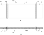
本実施形態における端子板20は、図2-aの平面図に示すように、一例として薄い銅板(銅箔や銅合金箔)を材料とし、コンデンサ素子10の陽極引出部13と陰極引出部14とほぼ合致する搭載ランドを有し、陽極電極部21を構成する金属板と陰極電極部22を構成する金属板が、絶縁性樹脂23によって絶縁されたものである。
本実施形態における端子板20は、図2-aの平面図に示すように、一例として薄い銅板(銅箔や銅合金箔)を材料とし、コンデンサ素子10の陽極引出部13と陰極引出部14とほぼ合致する搭載ランドを有し、陽極電極部21を構成する金属板と陰極電極部22を構成する金属板が、絶縁性樹脂23によって絶縁されたものである。
端子板20の内部構造は、図2-bの断面図に示すように、一枚の銅板から成る金属板の表裏は電気的に導通しており、陽極電極部21と陰極電極部22の間隙部に絶縁性樹脂23が入り込み絶縁を図るとともに、間隙部の樹脂と連続して銅板の表面の一部を覆うことで一体化を図っている。
すなわち、薄い金属板によって構成された陽極電極部21と、同じく薄い金属板によって構成された陰極電極部22を同一平面上に所定の幅の間隙を保って配置し、両者の間隙部分に絶縁性樹脂23を介在させ、この絶縁性樹脂23により陽極電極部21と陰極電極部22とを電気的に絶縁すると共に両電極をシート状に一体化したものである。
端子板20を構成する金属板としては、厚さが15μm~100μmの圧延銅箔を使用することが好ましい。また、絶縁性樹脂23は、端子板20を構成する金属板よりも、その両面とも所定の高さで突出した厚さとすることが陽極電極部21と陰極電極部22とを確実に一体化するという点では望ましい。しかし、金属板と同一の厚さ、あるいは金属板との接合部は金属板よりも厚く中央部は薄くなった鼓型の断面としても良い。絶縁性樹脂23の材質としては、ポリエステル樹脂やポリイミド樹脂を使用するが、必ずしもこれに限定されるものではない。絶縁性、金属板との密着性、強度などが、使用する固体電解コンデンサに適合するものであれば他の樹脂も使用可能である。
以下、このような構成を有する端子板20の製造方法の一例を示す。
(a)端子板20の陽極電極部21となる銅板と陰極電極部22となる銅板を離間させた状態で所定位置に配置する。
(b)絶縁性樹脂23を端子板20の陽極電極部21となる銅板と陰極電極部22となる銅板の間隙部を含む所定位置に塗布し、熱硬化する。この方法により陽極電極部21と陰極電極部22の絶縁を図るとともに、分離した陽極電極部21と陰極電極部21の一体化を図り、端子板20とする。
(a)端子板20の陽極電極部21となる銅板と陰極電極部22となる銅板を離間させた状態で所定位置に配置する。
(b)絶縁性樹脂23を端子板20の陽極電極部21となる銅板と陰極電極部22となる銅板の間隙部を含む所定位置に塗布し、熱硬化する。この方法により陽極電極部21と陰極電極部22の絶縁を図るとともに、分離した陽極電極部21と陰極電極部21の一体化を図り、端子板20とする。
この場合、絶縁性樹脂23の塗布位置は、銅板の陽極電極部21と陰極電極部22の間隙部、および間隙部の周囲部に塗布し、絶縁性樹脂23の厚さが、銅板よりも両面とも所定の高さの厚みで突出するように塗布すると好適である。また、銅板の露出部(搭載ランド)の形状は、コンデンサ素子10の陽極引出部13及び陰極引出部14に合致させた形状とする。
端子板20の陽極電極部21と陰極電極部22を所定位置に配置する際、その間隙部の幅は求められる特性に応じて任意に設定することができる。具体的には間隙部の幅は20μm程度にまで近接させて製造することが可能である。
(1-3)コンデンサ素子の端子板への搭載
図3に示すように、本実施形態の固体電解コンデンサは、前記コンデンサ素子10を端子板20に搭載して成る。コンデンサ素子10を端子板20に搭載するには銀ペースト等の導電性接着剤30により、接着を行うと好適である。この銀ペーストをコンデンサ素子10または端子板20に塗布して接着を図るが、この際に銀ペーストが流動して、陽極と陰極の短絡を引き起こすおそれもある。
図3に示すように、本実施形態の固体電解コンデンサは、前記コンデンサ素子10を端子板20に搭載して成る。コンデンサ素子10を端子板20に搭載するには銀ペースト等の導電性接着剤30により、接着を行うと好適である。この銀ペーストをコンデンサ素子10または端子板20に塗布して接着を図るが、この際に銀ペーストが流動して、陽極と陰極の短絡を引き起こすおそれもある。
しかし、本実施形態では、端子板20には絶縁性樹脂層23の厚さが銅板よりも両面とも所定の高さで突出するように形成されている。このため、絶縁性樹脂層23の突出部が、銀ペーストの流動を堰き止めるようになり、陽極電極部21と陰極電極部22の短絡を防止することができる。なお、絶縁性樹脂23の突出部の高さは任意であるが、突出する高さが高ければ、コンデンサ素子10を搭載した際の銀ペーストを堰き止める効果が高くなる。
さらに、本実施形態では、陽極電極部21と陰極電極部22の間隙部を絶縁性樹脂23によって絶縁するとともに、間隙部の周囲にも絶縁性樹脂23を形成することで、陽極と陰極の接合強度を高めている。その結果、端子板20の機械的強度が向上するとともに、コンデンサ素子を搭載する面での陽極電極部21と陰極電極部22の距離を離すことができる。その結果、端子板20にコンデンサ素子10を搭載し導電性接着剤30で接合した際に、陽極電極部21と陰極電極部22の絶縁をより確実に図ることができる。
(1-4)コンデンサ素子と端子板との接合構造
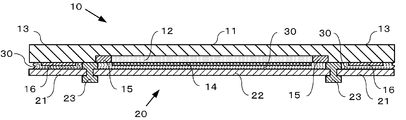
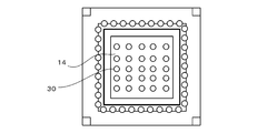
本実施形態の構成上の特徴は、図4に示すように、コンデンサ素子10の陽極引出部13および陰極引出部14と、端子板20の電極部21、22との間隙に、エポキシ樹脂などの絶縁樹脂31が充填された点にある。より詳しくは、コンデンサ素子10と端子板20を接合し熱硬化したとき、コンデンサ素子10と端子板20の間隔は20μm程度となるが、この間隙に絶縁樹脂31が充填される。なお、導電性接着材30は、直径300μm程度となるように、ほぼ300μmの間隔で、コンデンサ素子10の陰極引出部14に点状に塗布されている(図5に示した例では5×5箇所)。
本実施形態の構成上の特徴は、図4に示すように、コンデンサ素子10の陽極引出部13および陰極引出部14と、端子板20の電極部21、22との間隙に、エポキシ樹脂などの絶縁樹脂31が充填された点にある。より詳しくは、コンデンサ素子10と端子板20を接合し熱硬化したとき、コンデンサ素子10と端子板20の間隔は20μm程度となるが、この間隙に絶縁樹脂31が充填される。なお、導電性接着材30は、直径300μm程度となるように、ほぼ300μmの間隔で、コンデンサ素子10の陰極引出部14に点状に塗布されている(図5に示した例では5×5箇所)。
(2)本実施形態の作用効果
以上のような本実施形態の作用効果は次の通りである。すなわち、本実施形態によれば、コンデンサ素子10の陽極引出部13及び陰極引出部14から、電流の出口である端子板20の陽極電極部21及び陰極電極部22までの距離は、端子板20の厚さだけの距離で達成することができ、電流経路の短縮化を図ることができる。
以上のような本実施形態の作用効果は次の通りである。すなわち、本実施形態によれば、コンデンサ素子10の陽極引出部13及び陰極引出部14から、電流の出口である端子板20の陽極電極部21及び陰極電極部22までの距離は、端子板20の厚さだけの距離で達成することができ、電流経路の短縮化を図ることができる。
特に、端子板20の厚さは、15μm程度の銅板を用いることが可能なことから、コンデンサ素子10をリードフレームに取付けて樹脂モールドした場合に比べ、コンデンサ素子の陰極引出部から端子板の陰極電極部までの距離を極めて短くすることができる。また、端子板20は表裏が一体となった一枚の銅板であり、スルーホールによって表裏を連絡したフレキシブル基板よりも導通経路が多い。そのため、端子板20の表裏の間の電気抵抗は小さく、固体電解コンデンサの内部抵抗の低減が可能となる。
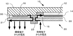
また、固体電解コンデンサを高周波回路の中で使用した場合、図6の拡大断面図に示すように、表皮効果によって、電流の高周波成分は端子板20の陽極電極部21と陰極電極部22の周縁部を流れる。本実施例の端子板20は陽極電極部21と陰極電極部22が所定の間隔をもって近接した構造となっており、特に高周波領域においては、陽極電極部21と陰極電極部22が近接することによる誘導磁界の相殺効果が大きく、固体電解コンデンサのESLの低減を図ることができる。この端子板20の陽極電極部21と陰極電極部22との間隙部の幅は、求められる特性に応じて任意に設定することが可能であるが、固体電解コンデンサのESL低減効果を得るためには、間隙部の幅は20~200μmの範囲に設定することが好適である。
本実施形態では、陽極電極部21と陰極電極部22の間隙部の周囲に絶縁性樹脂23を形成することで、陽極電極部21と陰極電極部22の接合強度が高まり、端子板20の機械的強度が向上する。絶縁性樹脂23を端子板10の間隙部に配置することで、コンデンサ素子10を搭載する面において陽極電極部21と陰極電極部22の距離を離すことができる。これにより、端子板20にコンデンサ素子10を搭載し導電性接着剤30で接合した際に、陽極電極部21と陰極電極部22の絶縁をより確実に図ることができる。また、導電性接着材30はドット状に塗布しているので、複数の導電経路を形成することができ、良好な過渡応答特性に寄与することができる。
なお、陽極電極部21と陰極電極部22は離間した形状となっているが、高周波電流が導体を流れる際の表皮効果によって、高周波電流は端子板10の陽極電極部21と陰極電極部22の周縁部を流れるため、両者の電流路自体は近接している。そのため、本実施例において、ESL低減効果が減少することはない。
さらに、本実施形態では、次のようなメリットがある。すなわち、コンデンサ素子10と端子板20の電極部21、22とを導電性接着材30により接合した上で、コンデンサ素子10と端子板20の間隙に絶縁樹脂31を充填している。このため、絶縁樹脂31が導電性接着材30の間に入り込む。絶縁樹脂31は、導電性接着材30に比べて、端子板20の電極部21、22との密着性が高く、コンデンサ素子10と端子板20を強固に密着させることができる。
したがって、半田リフロー時に高熱にさらされたことで、コンデンサ素子10の陰極引出部14から、ガス化した未重合モノマーや残留溶媒が、薄い金属の端子板20に向かって放出されても、ガスの圧力を、電性接着材30および電極部21、22と密着した絶縁樹脂31が受け止めることができる。
さらに、絶縁樹脂31はドット状に塗布された導電性接着材30の周囲に充填されるため、ガス圧力を分散させて受け止めることができる。したがって、気体圧力を十分に緩和することが可能である。この結果、端子板20は気体圧力が加わっても変形するおそれがなく、電極部21、22からの導電性接着材30の剥離を回避することができる。
以上説明したように、本実施形態によれば、電流経路を極力短くしたことで低ESL化を進めることができると同時に、コンデンサ素子10と端子板20との剥離を回避できるため、低ESR化も実現可能である。これにより、過渡応答性に優れ、高周波領域までインピーダンスの低い固体電解コンデンサを提供することができる。
(3)他の実施形態
本発明は、以上の実施形態に限定されるものではなく、絶縁樹脂の充填量や充填位置、構成部材の寸法や形状などは適宜自由である。例えば、コンデンサ素子10の陰極引出部14の形成位置は陽極体11中央に限らず、適宜変更可能である。また、導電性接着材30の塗布形状としては、図5に示したドット状以外にも、適宜選択可能である。具体的には図7に示すように導電性接着材32を星型にべた塗りすることで、接着面積の増大を図ることができる。つまり、陰極引出部14と陰極電極部22とを導電性接着剤30にて接続しているが、この導電性接着剤30を陰極引出部14と陰極電極部22との間に、絶縁樹脂31が充填可能な間隙を形成するような塗布形状であればよい。なお、陽極引出部13と陽極電極部21についても同様である。
本発明は、以上の実施形態に限定されるものではなく、絶縁樹脂の充填量や充填位置、構成部材の寸法や形状などは適宜自由である。例えば、コンデンサ素子10の陰極引出部14の形成位置は陽極体11中央に限らず、適宜変更可能である。また、導電性接着材30の塗布形状としては、図5に示したドット状以外にも、適宜選択可能である。具体的には図7に示すように導電性接着材32を星型にべた塗りすることで、接着面積の増大を図ることができる。つまり、陰極引出部14と陰極電極部22とを導電性接着剤30にて接続しているが、この導電性接着剤30を陰極引出部14と陰極電極部22との間に、絶縁樹脂31が充填可能な間隙を形成するような塗布形状であればよい。なお、陽極引出部13と陽極電極部21についても同様である。
なお、陽極引出部13と陰極引出部14の高さを調整するために、出発材料である陽極体11に予め凹部を形成し、この凹部の内部にエッチング層、誘電体酸化皮膜、固体電解質層、グラファイト層、銀ペースト層を形成して、高さを調整することも可能である。
このように、陽極体11の凹部に固体電解質層などを含む陰極引出部14を形成した場合、固体電解質層は金属材料からなる陽極体11の凹部に囲われているため、ガス化した未重合モノマーや残留溶媒が凹部の開口部側に向かって強く放出されることが多い。このような場合であっても、絶縁樹脂31の充填により導電性接着材30の剥離は確実に抑制される。そのため、コンデンサ素子10と端子板20との剥離を確実に防ぐことができ、固体電解コンデンサの内部での電気的抵抗が増加することがなく、ESR特性の上昇を抑えることができる。
しかも、上記実施形態では、陽極体11の凹部に陰極引出部14を形成したことで、端子板20を介して固体電解コンデンサの外部に陰極電極部22を引き出すことができる。このような固体電解コンデンサでは、コンデンサ素子10の誘電体酸化皮膜層から、固体電解コンデンサの外部端子までの距離を極めて短くすることができる。
さらに、コンデンサ素子10の陽極体11は凹部周囲を陽極部とし、この陽極部および端子板20の導体を介して、陽極電極部21として引き出すことができる。したがって、陽極、陰極ともに固体電解コンデンサの内部での導電経路が極めて短くなり、固体電解コンデンサの低ESL化を図ることができる。
10…コンデンサ素子
11…陽極体
12…エッチング層
13…陽極引出部
14…陰極引出部
15…分離層
16…金属片
20…端子板
21…陽極電極部
22…陰極電極部
23…絶縁性樹脂
30、32…導電性接着材
31…絶縁樹脂
11…陽極体
12…エッチング層
13…陽極引出部
14…陰極引出部
15…分離層
16…金属片
20…端子板
21…陽極電極部
22…陰極電極部
23…絶縁性樹脂
30、32…導電性接着材
31…絶縁樹脂
Claims (4)
- コンデンサ素子および端子板を備え、コンデンサ素子は、弁作用金属からなる陽極体の少なくとも片面に陰極部および陽極部を設け、前記陰極部には誘電体酸化皮膜層、固体電解質層、陰極引出部を順次形成して、該陰極部の周囲の前記陽極体の陽極部から陽極引出部を導出して構成し、前記端子板は、薄い金属板からなる陽極電極部および陰極電極部を同一平面上に間隙を保って配置し、前記陽極電極部と前記陰極電極部の間隙部に絶縁性樹脂を介在させ、この絶縁性樹脂により前記陽極電極部と前記陰極電極部とを電気的に絶縁すると共に両電極部をシート状に一体化して構成し、前記コンデンサ素子の接続面に前記端子板を重ね合わせた状態で、前記コンデンサ素子の陽極引出部に前記端子板の前記陽極電極部を、前記コンデンサ素子の陰極引出部に前記端子板の前記陰極電極部を、それぞれ電気的に接続した固体電解コンデンサにおいて、
前記陽極引出部と前記陽極電極部、並びに前記陰極引出部と前記陰極電極部を、それぞれ導電性接着材によって電気的に接続すると共に、前記コンデンサ素子と前記端子板の間隙を絶縁樹脂で充填したことを特徴とする固体電解コンデンサ。 - 前記コンデンサ素子は、前記陽極体の中央に凹部を形成し、この凹部内部に前記陰極引出部を形成し、前記凹部周囲の陽極体の端面を前記陽極引出部としたことを特徴とする請求項1に記載の固体電解コンデンサ。
- 前記導電性接着材を複数個所に塗布したことを特徴とする請求項1または2に記載の固体電解コンデンサ。
- 前記導電性接着材をドット状に複数塗布したことを特徴とする請求項3に記載の固体電解コンデンサ。
Applications Claiming Priority (2)
| Application Number | Priority Date | Filing Date | Title |
|---|---|---|---|
| JP2010-084586 | 2010-03-31 | ||
| JP2010084586A JP5526949B2 (ja) | 2010-03-31 | 2010-03-31 | 固体電解コンデンサ |
Publications (1)
| Publication Number | Publication Date |
|---|---|
| WO2011121980A1 true WO2011121980A1 (ja) | 2011-10-06 |
Family
ID=44711743
Family Applications (1)
| Application Number | Title | Priority Date | Filing Date |
|---|---|---|---|
| PCT/JP2011/001830 Ceased WO2011121980A1 (ja) | 2010-03-31 | 2011-03-28 | 固体電解コンデンサ |
Country Status (3)
| Country | Link |
|---|---|
| JP (1) | JP5526949B2 (ja) |
| TW (1) | TWI478187B (ja) |
| WO (1) | WO2011121980A1 (ja) |
Cited By (1)
| Publication number | Priority date | Publication date | Assignee | Title |
|---|---|---|---|---|
| JP2014203850A (ja) * | 2013-04-01 | 2014-10-27 | 日本ケミコン株式会社 | 固体電解コンデンサ及びその製造方法 |
Families Citing this family (1)
| Publication number | Priority date | Publication date | Assignee | Title |
|---|---|---|---|---|
| JP6492423B2 (ja) * | 2014-06-09 | 2019-04-03 | 日本ケミコン株式会社 | 固体電解コンデンサの製造方法 |
Citations (3)
| Publication number | Priority date | Publication date | Assignee | Title |
|---|---|---|---|---|
| JP2003158042A (ja) * | 2001-11-21 | 2003-05-30 | Japan Carlit Co Ltd:The | 三端子薄型アルミ固体電解コンデンサ |
| JP2009231337A (ja) * | 2008-03-19 | 2009-10-08 | Nec Tokin Corp | 固体電解コンデンサ |
| JP2009295645A (ja) * | 2008-06-02 | 2009-12-17 | Nippon Chemicon Corp | 固体電解コンデンサ |
-
2010
- 2010-03-31 JP JP2010084586A patent/JP5526949B2/ja active Active
-
2011
- 2011-03-28 WO PCT/JP2011/001830 patent/WO2011121980A1/ja not_active Ceased
- 2011-03-31 TW TW100111331A patent/TWI478187B/zh active
Patent Citations (3)
| Publication number | Priority date | Publication date | Assignee | Title |
|---|---|---|---|---|
| JP2003158042A (ja) * | 2001-11-21 | 2003-05-30 | Japan Carlit Co Ltd:The | 三端子薄型アルミ固体電解コンデンサ |
| JP2009231337A (ja) * | 2008-03-19 | 2009-10-08 | Nec Tokin Corp | 固体電解コンデンサ |
| JP2009295645A (ja) * | 2008-06-02 | 2009-12-17 | Nippon Chemicon Corp | 固体電解コンデンサ |
Cited By (1)
| Publication number | Priority date | Publication date | Assignee | Title |
|---|---|---|---|---|
| JP2014203850A (ja) * | 2013-04-01 | 2014-10-27 | 日本ケミコン株式会社 | 固体電解コンデンサ及びその製造方法 |
Also Published As
| Publication number | Publication date |
|---|---|
| JP5526949B2 (ja) | 2014-06-18 |
| TW201218226A (en) | 2012-05-01 |
| JP2011216742A (ja) | 2011-10-27 |
| TWI478187B (zh) | 2015-03-21 |
Similar Documents
| Publication | Publication Date | Title |
|---|---|---|
| JP4440911B2 (ja) | 固体電解コンデンサ | |
| US8213160B2 (en) | Solid electrolytic capacitor and method of manufacturing same | |
| JP2770636B2 (ja) | チップ型固体電解コンデンサ | |
| JP5007677B2 (ja) | 固体電解コンデンサ及びその製造方法 | |
| JP2014203850A (ja) | 固体電解コンデンサ及びその製造方法 | |
| JP5874280B2 (ja) | 固体電解コンデンサの製造方法 | |
| JP4508193B2 (ja) | 実装基板、実装体とそれを用いた電子機器 | |
| JP5526949B2 (ja) | 固体電解コンデンサ | |
| JP2009224688A (ja) | 固体電解コンデンサ | |
| WO2002078026A1 (en) | Solid electrolytic capacitor and method of manufacturing the capacitor | |
| JP4915856B2 (ja) | 固体電解コンデンサ | |
| CN111095452A (zh) | 固体电解电容器及其制造方法 | |
| JP5210672B2 (ja) | コンデンサ部品 | |
| JP4337423B2 (ja) | 回路モジュール | |
| US8724295B2 (en) | Solid electrolytic capacitor | |
| JP2010040960A (ja) | 固体電解コンデンサ | |
| JP2012182291A (ja) | 固体電解コンデンサ | |
| JPH06333789A (ja) | 低インピーダンス四端子型固体電解コンデンサ | |
| JP6492424B2 (ja) | 固体電解コンデンサの製造方法 | |
| JP5206008B2 (ja) | 固体電解コンデンサ及びその製造方法 | |
| JP5428471B2 (ja) | 固体電解コンデンサ及びその製造方法 | |
| JP2002299159A (ja) | 電源用レギュレータ | |
| JP2010219128A (ja) | 固体電解コンデンサ | |
| JP2005243889A (ja) | 固体電解コンデンサおよびその製造方法 | |
| JP2002299162A (ja) | 電源用レギュレータ |
Legal Events
| Date | Code | Title | Description |
|---|---|---|---|
| 121 | Ep: the epo has been informed by wipo that ep was designated in this application |
Ref document number: 11762228 Country of ref document: EP Kind code of ref document: A1 |
|
| NENP | Non-entry into the national phase |
Ref country code: DE |
|
| 122 | Ep: pct application non-entry in european phase |
Ref document number: 11762228 Country of ref document: EP Kind code of ref document: A1 |