WO2011111404A1 - 表示装置 - Google Patents
表示装置 Download PDFInfo
- Publication number
- WO2011111404A1 WO2011111404A1 PCT/JP2011/050057 JP2011050057W WO2011111404A1 WO 2011111404 A1 WO2011111404 A1 WO 2011111404A1 JP 2011050057 W JP2011050057 W JP 2011050057W WO 2011111404 A1 WO2011111404 A1 WO 2011111404A1
- Authority
- WO
- WIPO (PCT)
- Prior art keywords
- substrate
- display device
- terminal
- contact portion
- reference signal
- Prior art date
- Legal status (The legal status is an assumption and is not a legal conclusion. Google has not performed a legal analysis and makes no representation as to the accuracy of the status listed.)
- Ceased
Links
Images






Classifications
-
- G—PHYSICS
- G02—OPTICS
- G02F—OPTICAL DEVICES OR ARRANGEMENTS FOR THE CONTROL OF LIGHT BY MODIFICATION OF THE OPTICAL PROPERTIES OF THE MEDIA OF THE ELEMENTS INVOLVED THEREIN; NON-LINEAR OPTICS; FREQUENCY-CHANGING OF LIGHT; OPTICAL LOGIC ELEMENTS; OPTICAL ANALOGUE/DIGITAL CONVERTERS
- G02F1/00—Devices or arrangements for the control of the intensity, colour, phase, polarisation or direction of light arriving from an independent light source, e.g. switching, gating or modulating; Non-linear optics
- G02F1/01—Devices or arrangements for the control of the intensity, colour, phase, polarisation or direction of light arriving from an independent light source, e.g. switching, gating or modulating; Non-linear optics for the control of the intensity, phase, polarisation or colour
- G02F1/13—Devices or arrangements for the control of the intensity, colour, phase, polarisation or direction of light arriving from an independent light source, e.g. switching, gating or modulating; Non-linear optics for the control of the intensity, phase, polarisation or colour based on liquid crystals, e.g. single liquid crystal display cells
- G02F1/133—Constructional arrangements; Operation of liquid crystal cells; Circuit arrangements
- G02F1/1333—Constructional arrangements; Manufacturing methods
- G02F1/1345—Conductors connecting electrodes to cell terminals
-
- G—PHYSICS
- G02—OPTICS
- G02F—OPTICAL DEVICES OR ARRANGEMENTS FOR THE CONTROL OF LIGHT BY MODIFICATION OF THE OPTICAL PROPERTIES OF THE MEDIA OF THE ELEMENTS INVOLVED THEREIN; NON-LINEAR OPTICS; FREQUENCY-CHANGING OF LIGHT; OPTICAL LOGIC ELEMENTS; OPTICAL ANALOGUE/DIGITAL CONVERTERS
- G02F1/00—Devices or arrangements for the control of the intensity, colour, phase, polarisation or direction of light arriving from an independent light source, e.g. switching, gating or modulating; Non-linear optics
- G02F1/01—Devices or arrangements for the control of the intensity, colour, phase, polarisation or direction of light arriving from an independent light source, e.g. switching, gating or modulating; Non-linear optics for the control of the intensity, phase, polarisation or colour
- G02F1/13—Devices or arrangements for the control of the intensity, colour, phase, polarisation or direction of light arriving from an independent light source, e.g. switching, gating or modulating; Non-linear optics for the control of the intensity, phase, polarisation or colour based on liquid crystals, e.g. single liquid crystal display cells
- G02F1/133—Constructional arrangements; Operation of liquid crystal cells; Circuit arrangements
- G02F1/136—Liquid crystal cells structurally associated with a semi-conducting layer or substrate, e.g. cells forming part of an integrated circuit
- G02F1/1362—Active matrix addressed cells
- G02F1/136286—Wiring, e.g. gate line, drain line
-
- G—PHYSICS
- G11—INFORMATION STORAGE
- G11C—STATIC STORES
- G11C19/00—Digital stores in which the information is moved stepwise, e.g. shift registers
- G11C19/28—Digital stores in which the information is moved stepwise, e.g. shift registers using semiconductor elements
-
- G—PHYSICS
- G09—EDUCATION; CRYPTOGRAPHY; DISPLAY; ADVERTISING; SEALS
- G09G—ARRANGEMENTS OR CIRCUITS FOR CONTROL OF INDICATING DEVICES USING STATIC MEANS TO PRESENT VARIABLE INFORMATION
- G09G2310/00—Command of the display device
- G09G2310/02—Addressing, scanning or driving the display screen or processing steps related thereto
- G09G2310/0264—Details of driving circuits
- G09G2310/0286—Details of a shift registers arranged for use in a driving circuit
Definitions
- the present invention relates to a display device.
- This application claims priority on March 10, 2010 based on Japanese Patent Application No. 2010-053650 filed in Japan, the contents of which are incorporated herein by reference.
- a display device for example, a display device using a liquid crystal material or an organic electroluminescent material as a display medium layer, switching is performed for each of a plurality of pixels on a two-dimensional surface formed by a liquid crystal layer or an organic EL layer in order to increase the display capacity.
- An active matrix display device provided with an element is used.
- a counter data supply type liquid crystal display device in which an active element is provided for each pixel has also been proposed.
- This counter data supply type liquid crystal display device supplies data (video) signals to a plurality of stripe-shaped data electrodes provided on the counter substrate side among a pair of substrates arranged so as to sandwich a liquid crystal layer.
- a reference signal voltage common voltage
- FIG. 10 is a diagram showing the basic structure of this type of counter data supply type liquid crystal display device.
- pixel electrodes 101 are arranged in a matrix so as to correspond to the display area of one substrate 100 that sandwiches the liquid crystal layer.
- a common bus line 103 is connected to the source side of the switching element 102 connected to each pixel electrode 101 arranged in the row direction (X direction in FIG. 10).
- a gate bus line 105 is connected to the gate side of the switching elements 102 arranged in the row direction.
- a plurality of stripe-shaped data bus lines 107 extending in the column direction (Y direction in FIG. 10) are formed on the liquid crystal layer side of the opposite substrate 106 sandwiching the liquid crystal layer.
- An aggregate terminal portion 108 connected to the plurality of gate bus lines 105 is formed on the other substrate 100. Further, an aggregate terminal portion 109 connected to the plurality of data bus lines 107 is formed on the other substrate 106.
- a board such as a flexible printed circuit (FPC) on which a driving IC or the like is mounted, or the driving IC can be directly crimped and connected to the terminal portions 108 and 109.
- FPC flexible printed circuit
- the counter data supply type liquid crystal display device having the structure shown in FIG. 10 has a reference signal voltage (common to the common bus line 103 to the pixel electrode 101 via the switching element 102 turned on by the input from the gate bus line 105. Voltage) is applied. In addition, a corresponding data (video) signal is input to each of the plurality of data bus lines 107, and the liquid crystal present in the intersection region between the data bus lines 107 and the pixel electrodes 101 is driven to display.
- a reference signal voltage common to the common bus line 103 to the pixel electrode 101 via the switching element 102 turned on by the input from the gate bus line 105. Voltage
- a corresponding data (video) signal is input to each of the plurality of data bus lines 107, and the liquid crystal present in the intersection region between the data bus lines 107 and the pixel electrodes 101 is driven to display.
- the counter data supply type liquid crystal display device having the basic structure shown in FIG. 10 it is necessary to attach an FPC board and a driving IC to both of the
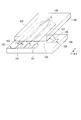
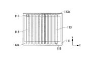
- FIGS. 11 shows the first substrate 111 on the opposite side
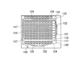
- FIG. 12 shows the second substrate 112 on the side where the switching elements are provided
- FIG. 13 shows an outline of the wiring structure when the two substrates are bonded together.
- a plurality of stripe-shaped data electrodes 113 extending in the column direction (Y direction) are provided on the liquid crystal layer side of the first substrate 111.
- a first end 113a and a second end 113b are formed at both ends in the length direction of each data electrode 113.
- a connection pad 115 is formed on the first end side, and a connection pad 116 is formed on the second end side.
- a plurality of pixel electrodes 117 are formed in a matrix on the liquid crystal layer side of the second substrate 112, and switching elements (not shown) electrically connected to the pixel electrodes 117 are formed.
- a plurality of stripe-shaped scanning lines 118 extending in the row direction along the pixel electrodes 117 and reference signal lines 119 arranged in parallel to the scanning lines 118 are formed. Has been.
- a seal portion 120 having a rectangular frame shape in plan view is formed outside the region where the display pixel electrodes 117 are arranged in a matrix.
- the substrates 111 and 112 are bonded to each other through the seal portion 120, and a liquid crystal layer is sandwiched and sealed between the substrates.
- an input terminal 121 is formed on one end side of the scanning line 118 and an input terminal 122 is formed on one end side of the reference signal line 119 so as to be drawn out of the seal portion 120 on the second substrate 112, and these terminals are shown in FIG. As shown, it is connected to a driving IC 123 mounted on the second substrate 112.
- connection pads 124 are provided along the upper side and the lower side of the seal portion 120, and these are the first substrate in a state where both substrates are bonded as shown in FIG.
- the data electrode input terminal 125 is formed on the connection pad 124 on the lower side of the second substrate 112 so as to be drawn to the outside of the seal portion 120, and these terminals are connected to the data electrodes 113 of the second substrate 112.
- Two driving ICs 126 mounted on the substrate 112 are connected.
- a spare wiring 130 for wiring correction is formed on the second substrate 112.
- each of the plurality of switching elements is formed between the reference signal line 119 and the pixel electrode 117, and is switched on by the input from the scanning line 118.
- a reference signal voltage common voltage
- a data (video) signal corresponding to each of the plurality of data electrodes 113 is input to each of the plurality of data electrodes 113 and displayed.
- the number of pixels of a recent digital television which is an application field of a liquid crystal display device, tends to increase, such as 1920 ⁇ 1080 or 1440 ⁇ 1080.
- the total number of data bus lines is 1980 ⁇ 3 when considering RGB display for color display for each pixel including wiring other than screen display. Is starting to be formed. If the counter data supply type liquid crystal display device having the structure shown in FIGS. 11 to 13 is applied to such a full HD compatible display panel, the total number of connection pads 116 and 124 formed on the counter substrate side is also increased. It becomes a huge number. In addition, a large number of locations for conducting the connection pads 116 and 124 are formed between the two substrates.
- the present invention was devised in view of the above problems, and its object is to provide a connection pad between a pair of substrates when a counter data supply type liquid crystal display device is applied to a panel structure having a large number of pixels.
- the display device of the present invention has been made in view of the above circumstances, and includes a first substrate, a second substrate disposed so as to face the first substrate, the first substrate, and the first substrate.
- a display medium layer provided between the substrate and a plurality of stripe-shaped data electrodes extending in a column direction on the first substrate, and a part of each of the data electrodes
- a first board-side terminal set part that is formed on the first board and that receives a data signal corresponding to each of the plurality of data electrodes; and the first board-side terminal set part
- the plurality of scanning lines and the plurality of reference signal lines, the plurality of pixel electrodes arranged in a matrix, and the plurality of scanning lines are turned on / off, and the plurality of reference signal lines and the plurality of reference signal lines are extended.
- a plurality of switching elements provided between the pixel electrode and a gate driver formed on the second substrate having a plurality of output terminals and connecting the output terminals to the scanning line;
- Contact portions are formed, and the first substrate and the second substrate are arranged so that the pixel electrodes arranged in a matrix and the data electrodes formed in a stripe are opposed to each other.
- the common bus line contact portion of the first substrate and the reference signal line contact portion of the second substrate are electrically connected, and the signal line contact portion of the first substrate and the The input terminal contact portion of the second substrate is electrically connected.
- the scanning line is scanned by the gate driver, and the switching element provided along the corresponding scanning line is turned on / off, and the reference is transmitted via the switching element in the on state.
- a reference signal voltage is applied to the pixel electrode from a signal line, and a corresponding data signal is input to each of the plurality of data electrodes, and the display is interposed between the pixel electrode and the data electrode to which the voltage is applied. It is possible to adopt a configuration characterized by controlling and displaying the transmittance of the medium layer.
- it can be set as the structure formed by connecting the flexible printed circuit board which mounted drive IC or drive IC to the said 1st board
- the gate driver includes a plurality of cascade-connected shift registers, each of which includes a clock input terminal, a signal input terminal, and an output terminal.
- a plurality of clock signals having different phases are supplied to the output circuit to switch the voltage at the output terminal between a high value and a low value.
- a scan start signal is input to the first-stage shift register
- a scan completion signal is input to a stage shift register
- the plurality of clock signals, the scan start signal, and the scan completion signal are input via an input terminal contact portion formed on the second substrate. It is good also as a structure.
- the number of conductive portions and the number of inter-substrate connection portions between the substrates that sandwich the display medium layer can be significantly reduced.
- a driving element such as a driving IC
- the display device can be driven. Therefore, it is necessary to separately provide the driving elements on both substrates. On the other hand, there is an effect that the drive element can be easily attached.
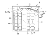
- FIG. 1A is a configuration diagram illustrating a display device according to an embodiment of the present invention.
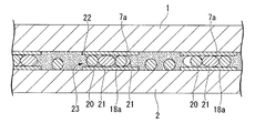
- FIG. 1B is a cross-sectional view illustrating an example of a conductive portion between substrates.
- FIG. 2 is a configuration diagram illustrating an example of a circuit configuration of a counter substrate provided in the display device of the embodiment.
- FIG. 3 is a configuration diagram illustrating an example of a circuit configuration of an element-side substrate provided in the display device of the embodiment.
- FIG. 4 is a diagram showing an equivalent circuit configuration of a portion including a pixel electrode and a switching element in the circuit configuration of the element side substrate provided in the display device of the embodiment.
- FIG. 5 is a configuration diagram showing an example of a circuit configuration when both substrates provided in the display device of the embodiment are integrated.
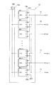
- FIG. 6 is a block circuit diagram showing an example of a multistage shift register when driving the display device of the embodiment.
- 7 is a circuit diagram illustrating an example of a transistor arrangement structure in each stage of the shift register illustrated in FIG.
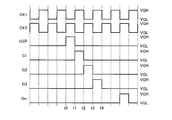
- FIG. 8 is a waveform diagram showing an example of input / output terminal voltages in the circuit of the shift register shown in FIG.
- FIG. 9 is a waveform diagram showing an example of drive waveforms and output pulses applied to the display device from the circuit shown in FIG.
- FIG. 10 is a block diagram showing an example of the basic structure of the counter data supply type liquid crystal display device.
- FIG. 11 is a configuration diagram showing the structure on the counter substrate side in the conventional structure example of the counter data supply type liquid crystal display device.
- FIG. 12 is a block diagram showing a structure on the element substrate side in a conventional structure example of a counter data supply type liquid crystal display device.
- FIG. 13 is a configuration diagram showing a circuit configuration when both substrates are integrated in a conventional structural example of a counter data supply type liquid crystal display device.
- FIG. 1A is a diagram showing an outline of both substrates in a state where both substrates are opposed to each other and wirings formed on both the substrates.
- FIG. 1B is a schematic cross-sectional view illustrating an example of the inter-substrate conductive portion.
- FIG. 2 is a diagram showing the wiring of the counter substrate.
- FIG. 3 is a diagram showing wiring of the element side substrate.
- FIG. 4 is a diagram showing a wiring structure around the pixel electrode.
- FIG. 5 is a schematic diagram showing an entire circuit as a display device when both substrates are combined.
- FIG. 6 shows a configuration example of a gate driver circuit applicable to the display device of this embodiment, and
- FIG. 7 shows an example of the internal transistor circuit.
- the display device A of the present embodiment is configured such that a rectangular first substrate 1 and a second substrate 2 face each other so as to sandwich a liquid crystal layer as a display medium layer.
- a sealing material a is disposed around the first substrate 1 and the second substrate 2. The liquid crystal layer is sealed between both the substrates 1 and 2 and the sealing material a.
- FIG. 1A shows the main parts of the wiring elements and electrode portions formed on the substrates 1 and 2.
- the first substrate 1 is usually composed of a transparent glass substrate or the like, but the second substrate 2 is a transparent substrate or a reflective substrate depending on whether the display method is a transmissive display type or a reflective display type. Select and use either non-transparent substrate.
- a plurality of stripe-shaped data electrodes (data lines) 3 extending in the column direction (Y direction in FIG. 1A) are provided on the surface of the first substrate 1 on the display medium layer side.
- the length direction one end 3a side of these data electrodes 3 is extended to the peripheral side of the first substrate 1 via the extension wiring 4, and the first substrate side terminal assembly 5 is formed at the peripheral side central side. Has been.
- the first board-side terminal assembly 5 is partitioned as a drive IC 25 (described later) or a flexible printed circuit board (FPC board) on which a drive IC and an electronic component are mounted, and the like.
- the driving IC 25 is fixed to the first substrate 1 and drives the plurality of data electrodes 3 on the first substrate 1 side.
- the first substrate 1 shown in FIG. 2 is a diagram in which the first substrate 1 shown in FIG. 1A is transmissively displayed and the wiring structure is mainly displayed. Therefore, the first substrate 1 shown in FIG. The left and right sides are displayed opposite to the view seen from the side.
- the common bus line contact portion 6 is disposed on the right side and the signal line contact portion 7 is disposed on the left side with respect to the plurality of arranged data electrodes 3. Is done.
- the common bus line contact portion 6 includes a terminal pad 6 a formed on the display medium layer side of the first substrate 1, and the terminal pad 6 a is connected to the first substrate side terminal assembly portion via an extension wiring 8. 5 and connected to the driving IC 25.
- the signal line contact portion 7 includes four terminal pads 7 a formed on the display medium layer side of the first substrate 1. These terminal pads 7 a are connected to the first board-side terminal assembly 5 via the extension wiring 9 and connected to the driving IC 25.
- a plurality of rectangular pixel electrodes 10 are formed in a matrix on the surface (upper surface) of the second substrate 2 on the display medium layer side as shown in FIGS. 1A and 3.
- pixel electrodes 10 a plurality of pixel electrodes 10 arranged at predetermined intervals in the column direction (Y direction) are arranged so as to correspond to the data electrodes 3 on the first substrate 1 side, and in the row direction.
- the interval between the pixel electrodes 10 arranged in the (X direction) is equal to the interval between the data electrodes 3 formed on the first substrate 1.
- a display device is configured by arranging an arbitrary number n of pixel electrodes in a matrix in the row direction. For example, in the case of a display device with a resolution of the full HD standard, the number of n is 1980 ⁇ 3 as a color display configuration using RGB color filters. Note that the arrangement number of the m ⁇ n pixel electrodes 10 in this embodiment can be adjusted as appropriate according to the resolution required for the display device, and thus this embodiment is merely an example.
- An appropriate number of arrays may be employed in accordance with the required resolution of the display device.
- a plurality of scanning lines 11 extending in the row direction (X direction) and a plurality of reference signal lines 12 extending in the row direction are provided.
- the pixel electrodes 10 are arranged along a matrix.
- Each scanning line 11 passes near the pixel electrode 10 and extends to the end side of the second substrate 2, and in the column direction (Y direction) on the right end side of the second substrate 2 shown in FIG. 1A.
- Each is connected to an output terminal of the gate driver 13 arranged so as to extend.
- FIG. 3 shows a state in which m scanning lines 11 are connected to the output terminal side of the gate driver 13, so that these scanning lines 11 are indicated with G1 to Gm for convenience. did.
- a switching element 15 such as a thin film transistor (TFT) element is disposed between each scanning line 11 and the pixel electrode 10 adjacent thereto. As shown in FIG. 4, the gate G of each switching element 15 is connected to the scanning line 11, and the drain D of each switching element 15 is connected to the pixel electrode 10.
- TFT thin film transistor
- the reference signal line 12 is formed along the row direction so as to pass through the vicinity of each pixel electrode 10 in parallel with the scanning line 11 as shown in FIGS. 1A and 4, and the switching element in the vicinity of each pixel electrode 10.
- the reference signal lines 12 are connected to an extension wiring 16 formed on the left end side of the second substrate 2.
- the extension wiring 16 is formed to extend in the column direction on the left end side of the second substrate 2, extends to a corner portion on the left end side of the second substrate 2, and has a reference signal line contact having a terminal pad 17 a at that position.
- a portion 17 is formed.
- the terminal pad 17a is formed in the same position as that of the terminal pad 6a formed on the first substrate 1 side in a state where the first substrate 1 and the second substrate 2 are arranged to face each other. It is a position that overlaps visually.
- the gate driver along the column direction (Y direction) of the second substrate 2 at a position corresponding to the one end side of the second substrate 2 and the one end side of the scanning line 11. 13 is disposed, and an input terminal contact portion 18 is formed in the vicinity of one end of the gate driver 13.
- Four terminal pads 18a are formed in the input terminal contact portion 18, and the four terminal pads 18a are connected to one end (input terminal side) of the gate driver 13 by connection lines 19a to 19d.
- the formation positions of these terminal pads 18a are the positions of the four terminal pads 7a formed on the first substrate 1 side in a state where the first substrate 1 and the second substrate 2 are arranged to face each other. It is a position that overlaps in a plan view.
- the conductive structure with the terminal pad 18a is the structure shown in FIG. 1B. That is, the spherical spacer 20 and the anisotropic conductive particles 21 are connected by the conductive material 23 having a structure in which a predetermined amount is dispersed inside the resin material 22. 1B shows the cross-sectional structure of the three terminal pads 18a and terminal pads 7a formed on the substrate 2, the terminal pads 6a of the first substrate 1 and the terminal pads 17a of the second substrate 2 are shown. Also in the connection portion, the terminal pad has an equivalent structure in which one terminal pad is formed on each substrate.
- the anisotropic conductive particles 21 are composed of composite particles in which a conductive layer such as Au is coated on the surface of a plastic particle having a predetermined particle size, and the first substrate 1 and the second substrate 2 Is interposed between the terminal pad 6a of the first substrate 1 and the terminal pad 17a of the second substrate 2 by the pressure applied when joining them, and is elastically deformed itself so that both are electrically connected. Connected. Further, the connection between the terminal pad 7a of the first substrate 1 and the terminal pad 18a of the second substrate 2 is also a connection structure using the conductive material 23.
- the anisotropic conductive particles 21 contained in the conductive material 23 is D particles / mm 2
- this blending amount is an example, and it is a matter of course that the conductive material 23 may be configured by blending a necessary and sufficient number for the low resistance connection as the display device A.
- the first substrate 1 and the second substrate 2 are opposed to each other with the display medium layer interposed therebetween, and the second substrate 2
- the reference signal line 12 of the substrate 2 is electrically connected to the first substrate-side terminal assembly 5 via the extension wiring 16, the terminal pad 17a, the conductive material 23, the terminal pad 6a, and the extension wiring 8, and the driving IC 25 Is electrically connected.
- the drive signal input terminal 13 a side of the gate driver 13 is electrically connected to the first substrate-side terminal assembly 5 via the connection line 19, the terminal pad 18 a, the conductive material 23, the terminal pad 7 a, and the extension wiring 9. Are electrically connected to the driving IC 25.
- a driving IC 25 for driving the display device A of the present application is terminal-connected to the first substrate-side terminal assembly 5 in the first substrate 1.
- the driving IC 25 supplies data signals to the plurality of data electrodes 3 on the first substrate 1 side, and issues a selection command as to which of the scanning lines 11 is to be selected to the gate driver 13. Has a function of applying a reference signal voltage.
- the driving IC 25 connected to the first board-side terminal assembly 5 may have a single IC configuration.
- the driving IC 25 may be a composite driving module in which a driving IC and other electronic components are mounted on an FPC board or the like.
- a sealing material a disposed between the substrates 1 and 2 for sealing liquid crystal is formed in a rectangular frame shape in plan view so as to surround the periphery of the pixel electrodes 10 arranged in a matrix. ing.
- Each side of the sealing material a is disposed on the inner side of the gate driver 13 and the terminal pad 18 a on the side where the gate driver 13 and the terminal pad 18 a are disposed on the substrate 2. Further, each side of the sealing material a is disposed on the inner side of the terminal pad 17a on the side where the terminal pad 17a is disposed on the substrate 2. In addition, each side of the sealing material a is disposed on the inner side of the substrate 1 on the side where the driving IC 25 is disposed, with respect to the installation position of the driving IC 25.
- a color filter in which RGB colors are arranged is normally arranged between the first substrate 1 and the data electrode 3.
- the description was omitted.
- a liquid crystal display device using a color-filter-on-array technology in which a color filter is provided on the second substrate 2 side is also provided.
- a structure provided on the substrate 2 side can also be employed.
- FIG. 6 is a block circuit diagram showing an example of the gate driver 13 having a basic structure in which the shift register SR is connected in multiple stages.
- the gate driver 13 includes a plurality of substantially identical cascade-connected first to m-th shift registers SR1 to SRm, each of which has a clock input terminal CKA and an output terminal. Q and input terminals S and R are provided. As shown in FIG.
- the clock signal CK1 is input to the clock input terminal CKA of the odd-numbered shift register SR such as the first, third, and fifth stages via the connection line 19a, and the second,
- the clock signal CK2 is input to the clock input terminal CKA of the even-numbered shift register SR as in the fourth and sixth stages through the connection line 19b.
- the scan start signal GSP1 is input to the input terminal S of the first-stage shift register SR1 through the connection line 19c.
- the branch output from the output terminal Q of the shift register SR of the next stage is inputted to the input terminal R of the shift register SR of each stage after the first stage.
- the branch output from the output terminal Q of the preceding shift register SR is input to the input terminal S of the second and subsequent stage shift registers SR.
- the scan completion signal GEP1 is input to the input terminal R of the last-stage shift register SRm via the connection line 19d.
- the output terminals Q of the first to m-th shift registers SR are connected to the scanning lines 11 formed on the substrate 2.
- the driving IC 25 connected to the first substrate-side terminal assembly 5 is configured to have the capability of generating the clock signal, the scanning start signal, and the scanning completion signal in addition to the capability of supplying the data signal.
- the driving IC 25 includes only a data signal supply capability, and a flexible printed circuit board including other element parts and a pulse generator in addition to the driving IC 25 is connected to the first board-side terminal assembly 5. It is also good.
- FIG. 7 An example of an internal transistor circuit structure in each shift register SR shown in FIG. 6 is shown in FIG.
- transistors M1 to M11 made of n-type TFTs are formed on the substrate 2 and connected to each other by wiring.
- a clock signal is input to the source of the transistor M1, and the drain of the transistor M2 is connected to the gate of the transistor M1 via the netA.
- the bias voltage VDD is applied to the source of the transistor M2, and the previous output (S (Gm-1)) is input to the gate of the transistor M2.
- the drain of the transistor M1 is connected to the gate of the transistor M11 via the output terminal Q.
- a capacitor C1 is connected between the output terminal Q and the node netA.
- the node netA is connected to the source of the transistor M3, and the gate of the transistor M3 is connected to the source of the transistor M7 and the gates of the transistors M4 and M8 via the node netB.
- the node netB is connected to the node netC through the capacitor C2.
- the node netC is connected to the source of the transistor M9, the source of the transistor M11, and the drain of the transistor M10, and a bias voltage VDD is applied to the source of the transistor M10.
- the transistor M8 shown in FIG. 7 is designed so that the transistor characteristics are similar to those of the transistor M3 or M4.
- W / L (channel width / channel length) of the transistors M3, M4, and M8 is made uniform, or in addition to the above, the layout arrangement of at least one of the transistors M3 and M4 and the transistor M8 is made close. It is possible to take the structure.
- the threshold voltage Vth of the transistors M3, M4, and M8 is the same (immediately before the circuit is operated), and the threshold value after the circuit is continuously operated for a certain period. The same applies to the voltage shift amount (Vth + ⁇ , ⁇ > 0).
- the scan start signal GSP1 or the output signal of the previous stage is input to the input terminal S of the shift register SR1.
- two drive pulses CK1 or CK2 having different phases are input to the clock signal input terminal CKA of the shift register SR of each stage.
- the drive pulse CK1 is input to the clock input terminal CKA of the odd-numbered shift register SR
- the drive pulse CK2 is input to the clock input terminal CKA of the even-numbered shift register SR.
- the signal output from the output terminal Q of the shift register SR at each stage is applied to the corresponding scanning lines G1 to Gm, and is output to the input terminal S of the shift register SR at the next stage.
- the potential of the scan start signal GSP1 becomes VGH.
- the transistors M2, M7, and M9 are turned on.
- the potential of the node netA is set to the potential VGH of the power supply line VDD. Therefore, the transistor M1 is in a conducting state, but the terminal voltage at the output terminal Q remains VGL because the terminal voltage at the input terminal CKA is VGL. Further, the transistor M7 becomes conductive, and the gate and drain of the transistor M8 are short-circuited, so that the transistor M8 is in a diode connection state.
- Vth_M8 is a threshold voltage of the transistor M8, and Vth_M8> 0 and Vth_M8> VGL.
- the voltage of the scan start signal GSP changes to VGL
- the voltage of the drive pulse CK1 changes to VGH.
- the transistors M2, M7, and M9 are turned off.
- the drain terminal voltage of the transistor M1 is set to VGH, the potential of the node netA is pulled up from VGH by the parasitic capacitance between the gate and drain of the transistor M1, and therefore the potential of the node netA is higher than VGH. (Ideally a voltage that is twice that of VGH, but does not increase to that voltage due to factors such as parasitic capacitance, resistance, etc. at node netA, input terminal CKA, output terminal Q, and transistor M1) .
- the potential VGH of the input terminal CKA is output to the output terminal Q through the transistor M1, the potential is applied to the corresponding scan line G1, and the scan line G1 is selected until the potential of the drive pulse CK1 changes to VGL at time t2. It becomes a state.
- the transistor M11 becomes conductive, the node netC becomes the source terminal voltage VGL of the transistor M11, and the state at time t0 can be maintained.
- the node netC can maintain the state at the time t0
- the node netB which is the other terminal of the capacitor C2
- the transistors M3 and M4 are turned off.
- the shift register SR2 This is the same as the state of the shift register SR1 at time t0.
- the voltage of the input terminal CKA is set to VGL.
- the potential of the node netA is higher than VGH and the drain terminal of the transistor M1 is set to VGL, current flows from the source terminal to the drain terminal of the transistor M1, and the drain terminal (output) of the transistor M1
- the potential at terminal Q) drops to VGL. Therefore, the potential of the scanning line G1 also drops to VGL, and the scanning line G1 is in a non-selected state. As a result, the transistor M11 is turned off.
- VGH is applied to the input terminal CKA
- the state is the same as at time t1 of the first-stage shift register SR1
- VGH is applied to the scanning line G2.
- the scanning line G2 is selected.
- VGL is applied to the input terminal R of the shift register SR1, and the transistor M10 is turned on, so that the node netC is set to the voltage VGH of the power supply line VDD. Accordingly, the voltage at the other terminal node netB of the capacitor C2 increases from the state at time t1 by the voltage increase at the node netC (VGH ⁇ VGL).
- the voltage of netB is Vth_M8 + VGH ⁇ VGL, and the transistors M3 and M4 are turned on. Accordingly, the potential of the node netA is set to the source terminal voltage VGL of the transistor M3, and the transistor M1 is turned off.
- the third-stage shift register SR3 is in the same state as the time t1 of the second-stage shift register SR2.
- the drive pulse CK1 changes to VGH
- the drive pulse CK2 changes to VGL.
- the voltage of the input terminal CKA in the first-stage shift register SR1 is set to VGH. Therefore, the gate terminal voltage (netA) of the transistor M1 is set to VGL, and the transistor M1 becomes non-conductive and the output terminal Q is maintained at VGL which is the source terminal voltage of the transistor M4.
- the second-stage shift register SR2 is in a state similar to that at time t2 of the first-stage shift register, VGL is applied to the scan line G2, and the scan line G2 is in a non-selected state.
- VGH is applied to the input terminal CKA, and a state similar to that at time t1 of the second-stage shift register SR2 is obtained. Therefore, since VGH is applied to the scanning line G3, the scanning line G3 is selected.
- the m-th shift register SRm at time t is the time t ⁇ of the previous stage (the previous stage) shift register SRm-1. 1 (the state is shifted), and functions as a shift register.
- the voltage at the input terminal R of the shift register SR1 rises to VGH, the transistor M10 becomes conductive, and netC It is impossible for the voltage to rise to VGH.
- the scanning terminal signal GEP1 is input to the input terminal R of the shift register SRm after the same state as the state of the shift register SR1 at the time t1, the state of the shift register SR1 at the time t2 is obtained. Accordingly, the scanning lines G1 to Gm can be terminated by setting the scanning line Gm by the shift register SRm to a non-selected state.
- the operation as the gate driver 13 can be performed by selectively scanning the scan lines G1 to Gm again in accordance with the next timing scan.
- the scanning lines 11 can be sequentially scanned in the display device A of the present embodiment. Therefore, in the display device A of the present embodiment, data signals are input to the plurality of data electrodes 3 of the first substrate 1 from the driving IC 25 connected to the first substrate-side terminal assembly 5, and the gate driver 13 is connected.
- the scanning line 11 is selected by driving to turn on the necessary switching element 15 and at the same time, a reference signal voltage (common voltage) is applied from the reference signal line 12 to the pixel electrode 10 connected to the switching element 15.
- a reference signal voltage common voltage
- the input terminal contact portion 18 connected to the driving signal input terminal of the gate driver 13 is several, for example, four connection lines. 19a to 19d. Therefore, it is not necessary to establish conduction with the conductive material between the first substrate 1 and the second substrate 2 for all the scanning lines 11, and if the number of conductive portions between the substrates is substantially four, the structure of the present embodiment. Can be realized. Thereby, the number of connections between the substrates can be greatly reduced.
- connection lines 19a are required. Since the connection between the scanning line substrates 1 and 2 can be completed by the conduction of ⁇ 19d, it contributes to significant labor saving. Further, if a driving element such as a driving IC is connected only to the first substrate side terminal assembly 5 on the first substrate 1 side, the display device A can be driven. In contrast to the conventional structure in which the drive elements need to be provided individually, there is an effect that the drive elements can be easily attached.
- the display device according to the present invention is suitable for a high-resolution display device such as full HD, and can improve the yield by reducing the number of conductive portions connected between the substrates.
Landscapes
- Physics & Mathematics (AREA)
- Nonlinear Science (AREA)
- Mathematical Physics (AREA)
- Chemical & Material Sciences (AREA)
- Crystallography & Structural Chemistry (AREA)
- General Physics & Mathematics (AREA)
- Optics & Photonics (AREA)
- Engineering & Computer Science (AREA)
- Microelectronics & Electronic Packaging (AREA)
- Liquid Crystal (AREA)
- Control Of Indicators Other Than Cathode Ray Tubes (AREA)
Abstract
Description
本願は、2010年3月10日に、日本に出願された特願2010-053650号に基づき優先権を主張し、その内容をここに援用する。
また、STN液晶表示装置型の改良タイプとして、画素毎にアクティブ素子を設けた構成の対向データ供給型の液晶表示装置も提案されている。
この対向データ供給型の液晶表示装置は、液晶層を挟持するように配置されている一対の基板のうち、対向基板側に設けられたストライプ状の複数のデータ電極にデータ(映像)信号が供給されるとともに、他方の基板側に設けられた複数のスイッチング素子を介してそれらのスイッチング素子に接続された画素電極に基準信号電圧(共通電圧)が供給されるタイプの液晶表示装置として知られている。
しかし、図10に示す基本構造の対向データ供給型液晶表示装置では、基板100、106の両方にそれぞれFPC基板や駆動用ICを装着して端子同士を圧着し接続する作業が必要になり、両方の基板に対する圧着作業の工程数の増加による液晶表示装置のコストアップが想定される問題がある。
このタイプの対向データ供給型液晶表示装置の一構造例を図11~図13に示す。
図11は対向側の第1基板111を示し、図12はスイッチング素子を設ける側の第2基板112を示し、図13は両基板を貼り合わせた場合の配線構造の概要を示す。
図11に示す如く第1基板111の液晶層側に列方向(Y方向)に延びたストライプ状の複数のデータ電極113が設けられている。また、各データ電極113の長さ方向両端に第1端部113aと第2端部113bが形成されている。また、第1端部側には接続パッド115が、第2端部側には接続パッド116が形成されている。
次に、図13に示す如く第2基板112の液晶層側にはマトリクス状に複数の画素電極117が形成されるとともに、各画素電極117に電気的に接続された図示略のスイッチング素子が形成されている。更に、第2基板112の液晶層側において各画素電極117に沿って行方向に延びたストライプ状の複数の走査線118と、該走査線118と平行に配置された基準信号線119とが形成されている。
このようなフルHD対応の表示パネルに対し、前述の図11~図13に示す構造の対向データ供給型液晶表示装置を適用しようとすると、対向基板側に形成する接続パッド116、124の総数も膨大な数となる。また、接続パッド116、124を導通するための箇所が両基板間に多数形成されることとなる。そのため、液晶パネル製造時の歩留まりの低下が懸念される。
例えば、液晶パネルの対になる基板間のパッド接続を行うためには、特許文献1にも記載の如く、プラスチックビーズ等のスペーサと異方性導電粒子を熱硬化型の樹脂中に混合し分散させてなる導通材を用い、液晶層を挟持するための基板を貼り合わせる際の圧力と温度条件を制御して対向させた基板の接続パッドどうしの間に配置した導通材を介し、接続パッドどうしの電気的接続を取っている。しかしながら、上述の如く接続パッド数が多くなると、接続不良を生じる確率が高くなり、歩留まりが低下するおそれがある。
(3)本発明において、前記第1の基板側端子集合部に駆動用ICあるいは駆動用ICを搭載したフレキシブルプリント基板が接続されてなる構成とすることができる。
(5)本発明において、前記第1の基板のコモンバスラインコンタクト部と前記第2の基板の基準信号線コンタクト部が、スペーサと異方性導電粒子とを樹脂中に分散させてなる導通材であって、前記第1の基板と前記第2の基板間に介装された導通材により電気的に接続されてなる構成とすることができる。
また、第1の基板側にのみ駆動用ICなどの駆動用素子の接続を行えば、表示装置の駆動ができるようになるので、両方の基板に個別に駆動用素子を設ける必要があった構造に対し、駆動用素子の取り付けも容易となる効果がある。
本実施形態の表示装置は、対になる基板間に液晶層などの表示媒体層が挟持される形態の対向データ供給型表示装置に適用される。図1Aは、両方の基板を対向させた状態の両基板と両基板に形成されている配線の概要を示す図である。図1Bは、基板間導通部分の一例を示す断面略図である。図2は、対向側基板の配線を示す図である。図3は、素子側基板の配線を示す図である。図4は、画素電極まわりの配線構造を示す図である。図5は、両基板を組み合わせた場合の表示装置としての全体回路を示す略図である。なお、図6に本実施形態の表示装置に適用可能なゲートドライバ回路の一構成例を示し、図7にその内部トランジスタ回路の一例を示す。
図1A、図2に示すように第1の基板1の表示媒体層側の面に、列方向(図1AのY方向)に延びたストライプ状の複数のデータ電極(データ線)3が設けられ、これらデータ電極3の長さ方向一端部3a側を第1の基板1の周辺部側に延長配線4を介し延出させて該周辺部中央側に第1の基板側端子集合部5が形成されている。この第1の基板側端子集合部5には後述する駆動用IC25あるいは駆動用ICと電子部品を搭載したフレキシブルプリント基板(FPC基板)等が端子接合される領域として区画されたものである。駆動用IC25は第1の基板1に固着され、第1の基板1側の複数のデータ電極3を駆動する。
なお、図2に示す第1の基板1は、図1Aに示す第1の基板1を透過表示して配線構造を主体として表示した図であるので、図1Aに示す第1の基板1を底面側から見た図とは左右が逆に表示してある。図1Aに示す第1の基板1を実際に底面から見た場合、配列された複数のデータ電極3に対し、コモンバスラインコンタクト部6は右側に配置され、信号ラインコンタクト部7は左側に配置される。
前記信号ラインコンタクト部7は、第1の基板1の表示媒体層側に形成された4つの端子パッド7aを具備している。そして、これらの各端子パッド7aが延長配線9を介して前記第1の基板側端子集合部5に接続され、駆動用IC25に接続されている。
これらの画素電極10のうち、列方向(Y方向)に所定の間隔をあけて配列された複数の画素電極10が第1の基板1側のデータ電極3と対応するように配置され、行方向(X方向)に配列されている画素電極10の間隔は第1の基板1に形成されているデータ電極3の間隔と同等とされている。なお、図1Aでは画素電極10の配列状態を簡略記載したので3つの画素電極のみを表記しているが、実際には適用する表示装置の解像度に合わせて図3に示す如く列方向に任意数m個、行方向に任意数n個の画素電極をマトリクス状に配置して表示装置が構成されている。これが例えば、フルHD規格の解像度の表示装置の場合、RGB方式のカラーフィルタを用いたカラー表示構成としてn数が1980×3となる。なお、この実施形態におけるm×n個の画素電極10の配列個数は表示装置に求められる解像度に応じて適宜調整できるので、本実施形態では一例を示したに過ぎない。要求される表示装置の解像度に合わせて適宜の数の配列を採用すれば良い。
次に、第2の基板2においてマトリクス状に配列されている画素電極10の近傍には、行方向(X方向)に延びる複数の走査線11と、行方向に延びる複数の基準信号線12が、マトリクス状に配列された各画素電極10に沿うように形成されている。
また、各走査線11とそれに近接する画素電極10との間に薄膜トランジスタ(TFT)素子などのスイッチング素子15が配置されている。また、図4に示す如く各スイッチング素子15のゲートGが走査線11に接続され、各スイッチング素子15のドレインDが画素電極10に接続されている。
即ち、球状のスペーサ20と異方性導電粒子21とを樹脂材22の内部に所定量分散させた構造の導通材23により接続されている。なお、図1Bでは基板2に3つ形成されている端子パッド18aと端子パッド7aの部分の断面構造を示したが、第1の基板1の端子パッド6aと第2の基板2の端子パッド17aの接続部分においても両基板に端子パッドが1つずつ形成された同等構造である。
そして、第1の基板1における第1の基板側端子集合部5に、本願の表示装置Aを駆動するための駆動用IC25が端子接続されている。この駆動用IC25は、第1の基板1側の複数のデータ電極3にデータ信号を供給するとともに、ゲートドライバ13に対しいずれかの走査線11を選択するのか選択指令を出し、基準信号線12に対して基準信号電圧を印加する機能を有する。
図1Aに示す如く前記基板1、2間に配置されて液晶を封止するためのシール材aは、マトリクス状に配列された画素電極10の周囲を囲むように平面視矩形枠状に形成されている。このシール材aの各辺は、基板2においてゲートドライバ13と端子パッド18aが配置されている側においてはゲートドライバ13及び端子パッド18aよりも内側に配置されている。また、シール材aの各辺は、基板2において端子パッド17aが配置されている側においては端子パッド17aよりも内側に配置されている。また、シール材aの各辺は、基板1において駆動用IC25が配置されている側においては駆動用IC25の設置位置よりも内側に配置されている。
図6はシフトレジスタSRを多段接続してなる基本構造からなるゲートドライバ13の一例を示すブロック回路図である。
この例のゲートドライバ13は、実質的に同一の複数のカスケード接続された第1~第m段のシフトレジスタSR1~SRmが配置されてなり、各シフトレジスタSRにそれぞれクロック入力端子CKAと出力端子Qと入力端子S、Rが各々設けられている。
図6に示すように第1段、第3段、第5段の如く奇数段のシフトレジスタSRのクロック入力端子CKAに、接続線19aを介してクロック信号CK1が入力され、第2段、第4段、第6段の如く偶数段のシフトレジスタSRのクロック入力端子CKAに、接続線19bを介してクロック信号CK2が入力される。また、第1段のシフトレジスタSR1の入力端子Sに接続線19cを介して走査スタート信号GSP1が入力される。また、第1段以降の各段のシフトレジスタSRの入力端子Rに次段のシフトレジスタSRの出力端子Qからの分岐出力が入力される。また、第2段以降のシフトレジスタSRの入力端子Sに前段のシフトレジスタSRの出力端子Qからの分岐出力が入力される。また、最終段のシフトレジスタSRmの入力端子Rには接続線19dを介して走査完了信号GEP1が入力される。
そして、前記第1段~第m段のシフトレジスタSRの各出力端子Qは基板2に形成されている各走査線11に接続されている。
図7に示すトランジスタ回路では、n型TFTからなるトランジスタM1~M11が基板2上に形成され相互に配線接続されている。トランジスタM1のソースにクロック信号が入力され、トランジスタM1のゲートにnetAを介してトランジスタM2のドレインが接続されている。また、トランジスタM2のソースにバイアス電圧VDDが印加され、トランジスタM2のゲートに前段の出力(S(Gm-1))が入力される。
トランジスタM1のドレインには出力端子Qを介してトランジスタM11のゲートが接続されている。また、出力端子QとノードnetAとの間にキャパシタC1が接続されている。
また、ノードnetAにはトランジスタM3のソースが接続され、トランジスタM3のゲートがノードnetBを介してトランジスタM7のソース及びトランジスタM4、M8のゲートに接続されている。また、ノードnetBは、キャパシタC2を介しノードnetCに接続されている。このノードnetCにトランジスタM9のソースとトランジスタM11のソースとトランジスタM10のドレインとが接続され、トランジスタM10のソースにバイアス電圧VDDが印加されている。
ここで、図7に示す回路においては簡略化のため、トランジスタM3、M4、M8の初期(回路を動作させる直前の)閾値電圧Vthが同じであり、ある期間回路を動作させ続けた後の閾値電圧シフト量(Vth+α、α>0)も同様であるとする。
そして、各段のシフトレジスタSRの出力端子Qから出力された信号は、それぞれ該当する走査ラインG1~Gmへ印加され、また次段のシフトレジスタSRの入力端子Sに出力される。
まず、時刻t0において走査スタート信号GSP1の電位がVGHとなる。この電位が第1段目のシフトレジスタSR1の入力端子Sに印加されると、トランジスタM2およびM7、M9が導通状態となる。このとき、ノードnetAの電位は電源線VDDの電位VGHに設定される。
従って、トランジスタM1は導通状態となるが、入力端子CKAの端子電圧がVGLのため、出力端子Qの端子電圧はVGLのままである。また、トランジスタM7が導通状態となり、トランジスタM8のゲート・ドレイン間が短絡されるため、トランジスタM8がダイオード接続状態となる。
従って、トランジスタM8のゲート・ドレイン端子(ノードnetB)からトランジスタM8のソース端子へ電流が流れ込み、ノードnetBは徐々に降下し、その電圧がVGL+Vth_M8となるまで降下し続ける。ここで、Vth_M8はトランジスタM8の閾値電圧であり、Vth_M8>0かつVth_M8>VGLである。
また、トランジスタM9が導通状態のためノードnetCはトランジスタM9のソース端子の電圧VGLに設定される。
また、トランジスタM1のドレイン端子電圧がVGHに設定されるため、トランジスタM1のゲート・ドレイン間に寄生する容量によってノードnetAの電位がVGHからプルアップされるため、ノードnetAの電位はVGHより大きい電位に設定される(理想的にはVGHの2倍の電圧になるが、ノードnetA、入力端子CKA、出力端子Q、トランジスタM1それぞれに寄生する容量、抵抗などの要因により、その電圧まで上がらない)。
また、次段のシフトレジスタSR2の入力端子Sには、シフトレジスタSR1の出力端子電圧Qの電圧が印加され、入力端子CKAには駆動パルスCK2の電圧が印加されるため、シフトレジスタSR2は、シフトレジスタSR1の時刻t0における状態と同様になる。
また、このとき次段のシフトレジスタSR2においては、入力端子CKAにVGHが印加され、1段目のシフトレジスタSR1の時刻t1と同様の状態となり、走査ラインG2にはVGHが印加されるため、走査ラインG2が選択状態となる。
これにより、シフトレジスタSR1は、入力端子RにVGLが印加され、トランジスタM10が導通状態となるため、ノードnetCが電源線VDDの電圧VGHに設定される。従って、キャパシタC2のもう一方の端子ノードnetBの電圧は、時刻t1の状態から、ノードnetCの電圧上昇分(VGH-VGL分)だけ上昇する。このとき、VGH>VGLの関係にあるため、netBの電圧は、Vth_M8+VGH-VGLとなり、トランジスタM3、M4が導通状態となる。よって、ノードnetAの電位がトランジスタM3のソース端子電圧VGLに設定され、トランジスタM1が非導通状態となる。
また、3段目のシフトレジスタSR3においては、2段目のシフトレジスタSR2の時刻t1と同様の状態となる。
2段目のシフトレジスタSR2は、1段目のシフトレジスタの時刻t2と同様の状態となり、走査ラインG2にVGLが印加され、走査ラインG2は非選択状態となる。
このとき3段目のシフトレジスタSR3においては、入力端子CKAにVGHが印加され、2段目のシフトレジスタSR2の時刻t1と同様の状態となる。よって、走査ラインG3にはVGHが印加されるため、走査ラインG3が選択状態となる。
また、最終段のシフトレジスタSRmにおいては、次の段のシフトレジスタが存在しないため、例えば時刻t2においてシフトレジスタSR1の入力端子Rの電圧がVGHに上昇し、トランジスタM10が導通状態となり、netCの電圧がVGHにまで上昇する、ということが起こり得ない。
従って、シフトレジスタSRmの入力端子Rには、時刻t1のシフトレジスタSR1の状態と同様の状態となった後、走査完了信号GEP1を入力することで、時刻t2におけるシフトレジスタSR1の状態となる。これによりシフトレジスタSRmによる走査ラインGmを非選択状態として走査ラインG1~Gmを走査終了させることができる。そして、次のタイミングの走査に合わせて再度走査ラインG1~Gmを選択走査することで、ゲートドライバ13としての動作を行うことができる。
Ids=W/L×μ×Cox×(Vgs-Vth_M8-Vds/2)×Vds…(1)式
ただし、(1)式において、μ:移動度、Cox:ゲート酸化膜容量、Vgs:ゲート・ソース間電圧、Vth:閾値電圧、Vds:ドレイン・ソース間電圧を示す。
Ids=W/L×μ×Cox×{(Vth_M8+VGH-VGL)+VGL-Vth_M8-Vds/2)×Vds
=W/L×μ×Cox×(VGH-Vds/2)×Vds・・・(2)式
つまり、トランジスタM8の閾値電圧に依存しない。この(2)式はトランジスタM3、M4について書き換えた式に対しても同様であることから、閾値シフトに関して無関係(トランジスタ駆動能力の劣化は無い)と言える。
従って、図7に示すトランジスタ回路を有するシフトレジスタSRを用いることで個々のトランジスタが閾値シフトを引き起こした場合にでも、シフトレジスタSRとしての機能を保つことができる。
従って、本実施形態の表示装置Aにおいて、第1の基板側端子集合部5に接続される駆動用IC25から第1の基板1の複数のデータ電極3にデータ信号を入力し、ゲートドライバ13を駆動して走査線11の選択を行ない、必要なスイッチング素子15をオン状態にすると同時に、スイッチング素子15に接続された画素電極10に対して基準信号線12から基準信号電圧(共通電圧)を印加することで、信号入力されたデータ線3と基準信号電圧が印加された画素電極10との交差部分に存在されている液晶層の液晶分子などの配向を制御し、光の透過率を制御して目的の映像などの表示を行うことができる。
従って、フルHD対応解像度の高精細表示装置において、走査線の数が極めて多い表示装置の構造であっても、基板間接続部の数を大幅に削減できることにより、歩留まりの向上効果を期待できる。例えば、高解像度の表示装置の場合、RGB方式のカラーフィルタを用いたカラー表示構成を考慮して数100本~数1000本もの走査線が必要な構造であっても、4本の接続線19a~19dの導通で走査線用の基板1、2間の接続を完成できるので、大幅な省力化に寄与する。
また、第1の基板1側の第1の基板側端子集合部5にのみ駆動用ICなどの駆動用素子の接続を行えば、表示装置Aの駆動ができるため、両方の基板1、2に個別に駆動用素子を設ける必要があった従来構造に対し、駆動用素子の取り付けも容易となる効果がある。
2 第2の基板
3 データ電極
4 延長配線
5 第1の基板側端子集合部
6 コモンバスラインコンタクト部
6a 端子パッド
7 信号ラインコンタクト部
8、9 延長配線
10 画素電極
11 走査線
12 基準信号線
13 ゲートドライバ
13a 駆動用信号入力端子
15 スイッチング素子
G ゲート
S ソース
D ドレイン
17 基準信号線コンタクト部
17a 端子パッド
18 入力端子コンタクト部
18a 端子パッド
19 接続線
19a、19b、19c、19d 接続線
21 異方性導電粒子
25 駆動用IC
Claims (5)
- 第1の基板と、前記第1の基板に対向するように配置された第2の基板と、前記第1の基板と第2の基板との間に設けられた表示媒体層とを有する表示装置であって、
前記第1の基板に、列方向に延びるストライプ形状の複数のデータ電極と、これらの各データ電極の一部から延出形成されて前記第1の基板に形成され、前記複数のデータ電極のそれぞれに対応するデータ信号が入力される第1の基板側端子集合部と、該第1の基板側端子集合部に接続するように前記第1の基板に形成されたコモンバスラインコンタクト部と、前記第1の基板側端子集合部に接続するように前記第1の基板に形成された信号ラインコンタクト部とが設けられるとともに、
前記第2の基板に、行方向に延びる、複数の走査線および複数の基準信号線と、マトリクス状に配置された複数の画素電極と、前記複数の走査線によってオン/オフが制御され、かつ、前記複数の基準信号線と前記複数の画素電極との間に設けられた複数のスイッチング素子と、複数の出力端子を有するとともにこれらの出力端子を前記走査線に接続して前記第2の基板に形成されたゲートドライバと、このゲートドライバの駆動用信号入力端子に接続するように前記第2の基板に形成された入力端子コンタクト部と、前記複数の基準信号線に接続するように前記第2の基板に形成された基準信号線コンタクト部とが形成され、
前記第1の基板と前記第2の基板が前記マトリクス状に配置された画素電極と前記ストライプ状に形成されたデータ電極とを対向させて配置された状態において、前記第1の基板のコモンバスラインコンタクト部と前記第2の基板の基準信号線コンタクト部とが電気的に接続されるとともに、前記第1の基板の信号ラインコンタクト部と前記第2の基板の入力端子コンタクト部が電気的に接続されてなることを特徴とする表示装置。 - 前記走査線を前記ゲートドライバにより走査して対応する走査線に沿って設けられている前記スイッチング素子のオン/オフ制御がなされ、オン状態のスイッチング素子を介して前記基準信号線から前記画素電極に基準信号電圧が印加されるとともに、前記複数のデータ電極にはそれぞれに対応するデータ信号が入力され、電圧印加された画素電極とデータ電極との間に介在された表示媒体層の透過率を制御して表示することを特徴とする請求項1に記載の表示装置。
- 前記第1の基板側端子集合部に駆動用ICあるいは駆動用ICを搭載したフレキシブルプリント基板が接続されてなることを特徴とする請求項1または2に記載の表示装置。
- 前記ゲートドライバが、カスケード接続された複数段のシフトレジスタを備えて構成され、各シフトレジスタにクロック入力端子及び信号入力端子と出力端子が形成され、前記シフトレジスタが、それらに位相の異なる複数のクロック信号が供給されて前記出力端子の電圧を高い値か、低い値かに切り替えるための出力回路であり、第1段のシフトレジスタに走査スタート信号が入力され、最終段のシフトレジスタに走査完了信号が入力されるように構成され、前記複数のクロック信号と前記走査スタート信号及び走査完了信号が前記第2の基板に形成された入力端子コンタクト部を介し入力される構成であることを特徴とする請求項1~3のいずれかに記載の表示装置。
- 前記第1の基板のコモンバスラインコンタクト部と前記第2の基板の基準信号線コンタクト部が、スペーサと異方性導電粒子とを樹脂中に分散させてなる導通材であって、前記第1の基板と前記第2の基板間に介装された導通材により電気的に接続されてなることを特徴とする請求項1~4のいずれか1項に記載の表示装置。
Priority Applications (3)
| Application Number | Priority Date | Filing Date | Title |
|---|---|---|---|
| US13/582,776 US20120327060A1 (en) | 2010-03-10 | 2011-01-05 | Display device |
| CN201180012660.6A CN102792357B (zh) | 2010-03-10 | 2011-01-05 | 显示装置 |
| JP2012504341A JP5344776B2 (ja) | 2010-03-10 | 2011-01-05 | 表示装置 |
Applications Claiming Priority (2)
| Application Number | Priority Date | Filing Date | Title |
|---|---|---|---|
| JP2010-053650 | 2010-03-10 | ||
| JP2010053650 | 2010-03-10 |
Publications (1)
| Publication Number | Publication Date |
|---|---|
| WO2011111404A1 true WO2011111404A1 (ja) | 2011-09-15 |
Family
ID=44563235
Family Applications (1)
| Application Number | Title | Priority Date | Filing Date |
|---|---|---|---|
| PCT/JP2011/050057 Ceased WO2011111404A1 (ja) | 2010-03-10 | 2011-01-05 | 表示装置 |
Country Status (4)
| Country | Link |
|---|---|
| US (1) | US20120327060A1 (ja) |
| JP (1) | JP5344776B2 (ja) |
| CN (1) | CN102792357B (ja) |
| WO (1) | WO2011111404A1 (ja) |
Cited By (2)
| Publication number | Priority date | Publication date | Assignee | Title |
|---|---|---|---|---|
| JP2017521717A (ja) * | 2014-07-17 | 2017-08-03 | 深▲セン▼市華星光電技術有限公司 | ブーストラップ機能を具えるゲート電極駆動回路 |
| JP2024170451A (ja) * | 2019-08-21 | 2024-12-10 | 京東方科技集團股▲ふん▼有限公司 | 表示基板及びその製造方法、表示装置 |
Families Citing this family (9)
| Publication number | Priority date | Publication date | Assignee | Title |
|---|---|---|---|---|
| US20130001546A1 (en) * | 2010-03-26 | 2013-01-03 | Tsuyoshi Kamada | Display device and method for producing array substrate for display device |
| CN104424876B (zh) * | 2013-08-22 | 2018-07-20 | 北京京东方光电科技有限公司 | 一种goa单元、goa电路及显示装置 |
| KR20160087043A (ko) * | 2015-01-12 | 2016-07-21 | 삼성디스플레이 주식회사 | 터치 센서를 포함하는 표시 장치 |
| US10586495B2 (en) * | 2016-07-22 | 2020-03-10 | Semiconductor Energy Laboratory Co., Ltd. | Display device and electronic device |
| TWI688812B (zh) * | 2018-11-21 | 2020-03-21 | 友達光電股份有限公司 | 顯示裝置 |
| CN110082965A (zh) * | 2019-04-08 | 2019-08-02 | 深圳市华星光电半导体显示技术有限公司 | 框胶硬化装置 |
| CN110047854B (zh) * | 2019-05-08 | 2021-02-23 | 深圳市华星光电半导体显示技术有限公司 | 显示面板及显示装置 |
| US12120918B2 (en) | 2019-06-28 | 2024-10-15 | Semiconductor Energy Laboratory Co., Ltd. | Display device |
| JP7441838B2 (ja) * | 2019-06-28 | 2024-03-01 | 株式会社半導体エネルギー研究所 | 表示装置 |
Citations (5)
| Publication number | Priority date | Publication date | Assignee | Title |
|---|---|---|---|---|
| JPH0616945U (ja) * | 1992-08-04 | 1994-03-04 | カシオ計算機株式会社 | 液晶表示装置 |
| WO2002039179A1 (en) * | 2000-11-08 | 2002-05-16 | Citizen Watch Co., Ltd. | Liquid crystal display apparatus |
| JP2003216062A (ja) * | 2002-01-18 | 2003-07-30 | Sharp Corp | 表示装置 |
| JP2006220702A (ja) * | 2005-02-08 | 2006-08-24 | Seiko Epson Corp | 液晶表示装置の製造方法、液晶表示装置および電子機器 |
| WO2009093352A1 (ja) * | 2008-01-24 | 2009-07-30 | Sharp Kabushiki Kaisha | 表示装置及び表示装置の駆動方法 |
Family Cites Families (5)
| Publication number | Priority date | Publication date | Assignee | Title |
|---|---|---|---|---|
| FR2553218B1 (fr) * | 1983-10-07 | 1987-09-25 | Commissariat Energie Atomique | Ecran d'affichage a matrice active sans croisement des lignes et des colonnes d'adressage |
| US7088330B2 (en) * | 2000-12-25 | 2006-08-08 | Sharp Kabushiki Kaisha | Active matrix substrate, display device and method for driving the display device |
| JP2002333639A (ja) * | 2001-03-08 | 2002-11-22 | Sharp Corp | 液晶表示装置 |
| JP4225777B2 (ja) * | 2002-02-08 | 2009-02-18 | シャープ株式会社 | 表示装置ならびにその駆動回路および駆動方法 |
| JP5130916B2 (ja) * | 2008-01-08 | 2013-01-30 | 三菱電機株式会社 | アクティブマトリクス用走査線駆動回路 |
-
2011
- 2011-01-05 CN CN201180012660.6A patent/CN102792357B/zh not_active Expired - Fee Related
- 2011-01-05 WO PCT/JP2011/050057 patent/WO2011111404A1/ja not_active Ceased
- 2011-01-05 JP JP2012504341A patent/JP5344776B2/ja not_active Expired - Fee Related
- 2011-01-05 US US13/582,776 patent/US20120327060A1/en not_active Abandoned
Patent Citations (5)
| Publication number | Priority date | Publication date | Assignee | Title |
|---|---|---|---|---|
| JPH0616945U (ja) * | 1992-08-04 | 1994-03-04 | カシオ計算機株式会社 | 液晶表示装置 |
| WO2002039179A1 (en) * | 2000-11-08 | 2002-05-16 | Citizen Watch Co., Ltd. | Liquid crystal display apparatus |
| JP2003216062A (ja) * | 2002-01-18 | 2003-07-30 | Sharp Corp | 表示装置 |
| JP2006220702A (ja) * | 2005-02-08 | 2006-08-24 | Seiko Epson Corp | 液晶表示装置の製造方法、液晶表示装置および電子機器 |
| WO2009093352A1 (ja) * | 2008-01-24 | 2009-07-30 | Sharp Kabushiki Kaisha | 表示装置及び表示装置の駆動方法 |
Cited By (3)
| Publication number | Priority date | Publication date | Assignee | Title |
|---|---|---|---|---|
| JP2017521717A (ja) * | 2014-07-17 | 2017-08-03 | 深▲セン▼市華星光電技術有限公司 | ブーストラップ機能を具えるゲート電極駆動回路 |
| JP2024170451A (ja) * | 2019-08-21 | 2024-12-10 | 京東方科技集團股▲ふん▼有限公司 | 表示基板及びその製造方法、表示装置 |
| JP7827790B2 (ja) | 2019-08-21 | 2026-03-10 | 京東方科技集團股▲ふん▼有限公司 | 表示基板及びその製造方法、表示装置 |
Also Published As
| Publication number | Publication date |
|---|---|
| US20120327060A1 (en) | 2012-12-27 |
| CN102792357A (zh) | 2012-11-21 |
| CN102792357B (zh) | 2014-11-26 |
| JP5344776B2 (ja) | 2013-11-20 |
| JPWO2011111404A1 (ja) | 2013-06-27 |
Similar Documents
| Publication | Publication Date | Title |
|---|---|---|
| JP5344776B2 (ja) | 表示装置 | |
| US8471981B2 (en) | Display apparatus and display set having the same | |
| KR102034112B1 (ko) | 액정 디스플레이 장치와 이의 구동방법 | |
| US10073556B2 (en) | Liquid crystal display device with touch panel | |
| JP4668892B2 (ja) | 液晶表示装置及びその駆動方法 | |
| US10593281B2 (en) | Drive circuit, display device, and drive method | |
| CN110658658B (zh) | 图像显示装置 | |
| US8054393B2 (en) | Liquid crystal display device | |
| CN113393790A (zh) | 显示面板的驱动方法、装置及显示装置 | |
| US8619014B2 (en) | Liquid crystal display device | |
| CN107077821B (zh) | 有源矩阵基板及包含其之显示装置 | |
| CN106328082A (zh) | 显示装置 | |
| CN109308884B (zh) | 无驱动芯片的显示装置 | |
| CN119137536B (zh) | 阵列基板、驱动方法和显示装置 | |
| JP4163611B2 (ja) | 液晶表示装置 | |
| JP5172212B2 (ja) | 液晶表示装置 | |
| JP2017040881A (ja) | 駆動回路、表示装置及び駆動方法 | |
| JP2010054527A (ja) | 表示装置及びその表示駆動方法 | |
| CN113393788A (zh) | 显示面板的驱动方法、装置及显示装置 | |
| CN102136242A (zh) | 平面显示面板、像素电路及压差驱动元件的驱动方法 | |
| CN118016022A (zh) | 栅极驱动电路、阵列基板及显示面板 | |
| US20090059106A1 (en) | Liquid crystal device, driving method of liquid crystal device, integrated circuit device for driving liquid crystal device, and electronic apparatus | |
| CN119943001B (zh) | 显示装置 | |
| JP4919607B2 (ja) | 液晶表示装置 | |
| US12008972B2 (en) | Display device |
Legal Events
| Date | Code | Title | Description |
|---|---|---|---|
| WWE | Wipo information: entry into national phase |
Ref document number: 201180012660.6 Country of ref document: CN |
|
| 121 | Ep: the epo has been informed by wipo that ep was designated in this application |
Ref document number: 11753067 Country of ref document: EP Kind code of ref document: A1 |
|
| WWE | Wipo information: entry into national phase |
Ref document number: 2012504341 Country of ref document: JP |
|
| WWE | Wipo information: entry into national phase |
Ref document number: 13582776 Country of ref document: US |
|
| NENP | Non-entry into the national phase |
Ref country code: DE |
|
| 122 | Ep: pct application non-entry in european phase |
Ref document number: 11753067 Country of ref document: EP Kind code of ref document: A1 |