WO2011111193A1 - 無線装置及び無線送信制御方法 - Google Patents
無線装置及び無線送信制御方法 Download PDFInfo
- Publication number
- WO2011111193A1 WO2011111193A1 PCT/JP2010/054043 JP2010054043W WO2011111193A1 WO 2011111193 A1 WO2011111193 A1 WO 2011111193A1 JP 2010054043 W JP2010054043 W JP 2010054043W WO 2011111193 A1 WO2011111193 A1 WO 2011111193A1
- Authority
- WO
- WIPO (PCT)
- Prior art keywords
- unit
- signal
- signal level
- power amplifier
- correction
- Prior art date
- Legal status (The legal status is an assumption and is not a legal conclusion. Google has not performed a legal analysis and makes no representation as to the accuracy of the status listed.)
- Ceased
Links
Images



Classifications
-
- H—ELECTRICITY
- H03—ELECTRONIC CIRCUITRY
- H03G—CONTROL OF AMPLIFICATION
- H03G3/00—Gain control in amplifiers or frequency changers
- H03G3/20—Automatic control
- H03G3/30—Automatic control in amplifiers having semiconductor devices
- H03G3/3036—Automatic control in amplifiers having semiconductor devices in high-frequency amplifiers or in frequency-changers
- H03G3/3042—Automatic control in amplifiers having semiconductor devices in high-frequency amplifiers or in frequency-changers in modulators, frequency-changers, transmitters or power amplifiers
-
- H—ELECTRICITY
- H04—ELECTRIC COMMUNICATION TECHNIQUE
- H04B—TRANSMISSION
- H04B1/00—Details of transmission systems, not covered by a single one of groups H04B3/00 - H04B13/00; Details of transmission systems not characterised by the medium used for transmission
- H04B1/02—Transmitters
- H04B1/04—Circuits
- H04B1/0458—Arrangements for matching and coupling between power amplifier and antenna or between amplifying stages
Definitions
- the present invention relates to a wireless device and a wireless transmission control method.
- a wireless device such as a mobile phone transmits a signal of a predetermined power to a base station.
- a wireless device such as a mobile phone transmits a signal of a predetermined power to a base station.
- the wireless device controls the power to be transmitted to the base station based on the power set in the TPC.
- TPC Transmission Power Control
- a circuit such as a coupler in the wireless device feeds back a traveling wave output from the power amplifier to the control unit.
- a control unit controls the gain of a variable gain amplifier (VGA) arranged in front of the power amplifier based on the fed-back traveling wave.
- VGA variable gain amplifier
- the controller adjusts the power of the signal input to the power amplifier by controlling the gain of the variable gain amplifier, and as a result, adjusts the power of the signal output from the power amplifier.
- APC Auto Power Control
- the load (impedance) of the antenna installed in the wireless device fluctuates when an obstacle such as a human body approaches or contacts the antenna.
- a reflected wave is generated from the antenna in the direction of the power amplifier, and as a result, distortion occurs in the signal output from the power amplifier.
- a signal transmitted from the wireless device to the base station deteriorates.
- some conventional wireless apparatuses are provided with an isolator for blocking the reflected wave between the power amplifier and the antenna.
- a technique for suppressing distortion of the output signal of the power amplifier without using an isolator has been proposed.
- a radio apparatus has been proposed that variably controls a power supply voltage applied to a power amplifier based on the power of a reflected signal and the phase of the reflected signal. Such a radio apparatus suppresses distortion generated in a transmission signal without using an isolator even when a load fluctuation occurs in the antenna.
- the above prior art has a problem that power consumption increases. Specifically, the above-described wireless device without an isolator controls APC control and the voltage applied to the power amplifier even when the transmission power is low or the load fluctuation of the antenna is small. That is, since the conventional wireless device performs APC control and applied voltage control even when the transmission signal is not distorted, power consumption may increase.
- the disclosed technology has been made in view of the above, and an object thereof is to provide a wireless device and a wireless transmission control method capable of reducing power consumption.
- a wireless device disclosed in the present application is a power amplifier that amplifies an input signal and outputs the amplified signal to an antenna, an acquisition unit that acquires a signal level of a transmission signal specified from an external device, and the power amplifier A reflected wave detection unit that detects a reflected wave reflected from the antenna toward the power amplifier, and a reflected wave detected by the reflected wave detection unit.
- a correction unit that corrects the voltage applied to the power amplifier according to the signal level of the power amplifier, and determines whether the signal level acquired by the acquisition unit is equal to or higher than a first threshold, and the signal level is When the value is equal to or higher than the first threshold, the determination unit determines whether the signal level of the reflected wave detected by the reflected wave detection unit is equal to or higher than the second threshold, and the determination unit The correction unit is stopped when it is determined that the signal level of the transmission signal is lower than the first threshold, or when the signal level of the reflected wave is determined to be lower than the second threshold by the determination unit. And a stop unit to perform.
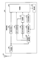
- FIG. 1 is a block diagram illustrating a configuration example of a wireless device according to the first embodiment.
- FIG. 2 is a block diagram illustrating a configuration example of a wireless device according to the second embodiment.
- FIG. 3 is a block diagram illustrating a configuration example of the control unit illustrated in FIG. 2.
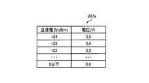
- FIG. 4 is a diagram illustrating an example of the power supply unit control table.
- FIG. 5 is a diagram illustrating an example of the power supply unit correction table.
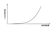
- FIG. 6 is a diagram illustrating the relationship between the antenna load fluctuation and the correction unit output.
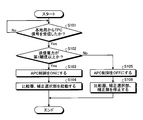
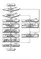
- FIG. 7 is a flowchart illustrating a start / stop processing procedure of APC control performed by the wireless device according to the second embodiment.
- FIG. 8 is a flowchart illustrating a transmission processing procedure performed by the wireless apparatus according to the second embodiment.
- FIG. 1 is a block diagram illustrating a configuration example of a wireless device according to the first embodiment.
- the wireless device 100 illustrated in FIG. 1 is a communication device such as a mobile phone or a PDA (Personal Digital Assistant).
- the wireless device 100 includes an antenna 101, a power amplifier 102, an acquisition unit 103, a reflected wave detection unit 104, a correction unit 105, a determination unit 106, and a stop unit 107.
- the antenna 101 emits a transmission signal into the air and receives a signal transmitted from an external device.
- the power amplifier 102 amplifies the input signal and outputs the amplified signal to the antenna 101.
- the acquisition unit 103 acquires the signal level of the transmission signal of the wireless device 100 designated from the external device.
- “signal level” indicates, for example, signal power or voltage.
- the antenna 101 receives a signal including TPC from an external device such as a base station.
- the acquisition unit 103 acquires the signal level of the signal transmitted by the wireless device 100 from the signal including the TPC received by the antenna 101.
- a signal including TPC may be referred to as a “TPC signal”.
- the reflected wave detection unit 104 detects a reflected wave in which a part of a traveling wave that is a signal output to the antenna 101 by the power amplifier 102 is reflected from the antenna 101 toward the power amplifier 102.
- the correction unit 105 corrects the voltage applied to the power amplifier 102 according to the signal level of the reflected wave detected by the reflected wave detection unit 104. For example, the correction unit 105 corrects so that the voltage applied to the power amplifier 102 increases as the signal level of the reflected wave increases.
- the determination unit 106 determines whether the signal level acquired by the acquisition unit 103 is equal to or higher than the first threshold value. When the signal level is equal to or higher than the first threshold, the determination unit 106 determines whether the signal level of the reflected wave detected by the reflected wave detection unit 104 is equal to or higher than the second threshold.
- the stopping unit 107 is used when the determination unit 106 determines that the signal level of the transmission signal is lower than the first threshold, or when the determination unit 106 determines that the signal level of the reflected wave is lower than the second threshold.
- the correction unit 105 is stopped.
- the correction unit 105 does not correct the voltage applied to the power amplifier 102 when the transmission signal level of the wireless device 100 specified by the external device is smaller than the first threshold value.
- the correction unit 105 determines that the reflected wave signal level is lower than the second threshold value, the power amplifier 102 The applied voltage is not corrected.
- the correction unit 105 applies the voltage applied to the power amplifier 102 when the transmission signal level specified from the external device is equal to or higher than the first threshold value and the signal level of the reflected wave is equal to or higher than the second threshold value. Correct.
- the wireless device 100 when the signal level of the transmission signal designated by the external device is smaller than the first threshold, the wireless device 100 according to the first embodiment stops the correction unit 105 and switches to the power amplifier 102. The applied voltage is not corrected. The reason why the applied voltage is not corrected when the signal level of the transmission signal is smaller than the first threshold will be described below.
- the power amplifier 102 is more likely to cause temperature fluctuations as the power of the input signal is larger, and as a result, there is a higher possibility of outputting a signal including distortion. That is, as the signal level specified from the external device is larger, the signal level of the signal input to the power amplifier 102 is higher, so that the power amplifier 102 is more likely to output a signal including distortion.
- the distortion characteristic of the power amplifier 102 improves as the voltage applied to the power amplifier 102 increases. That is, distortion included in the output signal of the power amplifier 102 is suppressed as the voltage applied to the power amplifier 102 is higher. Therefore, for example, the correction unit 105 corrects the distortion included in the output signal of the power amplifier 102 by correcting the voltage applied to the power amplifier 102 as the signal level specified by the external device increases. Suppress.
- the power amplifier 102 is less likely to output a signal including distortion when a signal smaller than a predetermined signal level is input. This is because the power amplifier 102 is unlikely to generate nonlinear distortion and out-of-band radiation due to saturation when the signal level of the input signal is smaller than a predetermined value. That is, when the signal level designated from the external device is small, the power amplifier 102 is unlikely to output a signal including distortion.
- the wireless device 100 stops the correction unit 105 and does not correct the voltage applied to the power amplifier 102. Even when the signal level specified by the external device is small, the power amplifier 102 may output a signal including distortion. However, when the signal level of the input signal is small, the power amplifier 102 is unlikely to output a signal that does not satisfy the conditions defined between the radio apparatus 100 and the base station.
- the first threshold value is a signal level threshold value of a transmission signal designated from an external device. For example, even when the correction process by the correction unit 105 is not performed, if the signal level of the transmission signal specified by the external device is smaller than the first threshold, the wireless device 100 is in communication with the base station.
- the first threshold value is set so that a signal satisfying the protocol can be transmitted.
- the radio apparatus 100 stops the correction unit 105 when the signal level of the reflected wave is smaller than the second threshold value even if the signal level of the transmission signal is equal to or higher than the first threshold value.
- the voltage applied to the power amplifier 102 is not corrected. This is because the smaller the signal level of the reflected wave is, the smaller the load variation of the antenna 101 is, and the possibility that the power amplifier 102 outputs a signal including distortion is low.
- the second threshold value is a threshold value of the reflected wave signal level. For example, even when correction processing by the correction unit 105 is not performed, if the signal level of the reflected wave is smaller than the second threshold, the radio apparatus 100 transmits a signal that satisfies the protocol with the base station.
- a second threshold is set so that it is possible.
- the wireless device 100 uses the power amplifier 102 when the signal level specified by the external device is equal to or higher than the first threshold and the signal level of the reflected wave is equal to or higher than the second threshold. Correct the applied voltage. This is because there is a high possibility that the power amplifier 102 outputs a signal including distortion under such conditions. Thereby, the radio
- the radio apparatus 100 stops the correction unit 105 and applies it to the power amplifier 102 when the possibility that distortion is generated in the signal output from the power amplifier 102 is low.
- the voltage is not corrected. That is, when there is a low possibility that distortion occurs in the signal output from the power amplifier 102, the radio apparatus 100 does not increase the voltage applied to the power amplifier 102, so that power consumption can be reduced.
- the radio apparatus 100 corrects the voltage applied to the power amplifier 102 when there is a high possibility that the signal output from the power amplifier 102 is distorted. Thereby, the radio
- FIG. 2 is a block diagram illustrating a configuration example of a wireless device according to the second embodiment.
- the wireless device 200 illustrated in FIG. 2 is a communication device such as a mobile phone or a PDA.
- the wireless device 200 includes an antenna 201, an antenna sharing unit 202, and a reception circuit unit 203.
- the antenna 201 transmits / receives various signals to / from an external device.
- the antenna 201 emits a transmission signal into the air.
- the antenna 201 receives a signal transmitted from an external device.
- the antenna sharing unit 202 makes the antenna 201 usable for both signal transmission and reception. Specifically, antenna sharing section 202 outputs a transmission signal input from directional coupler 240 described later to antenna 201. Further, the antenna sharing unit 202 outputs a signal received by the antenna 201 to the reception circuit unit 203.
- the receiving circuit unit 203 performs various processes on the signal received by the antenna 201. For example, the reception circuit unit 203 performs demodulation processing on the received signal.
- the receiving circuit unit 203 in the second embodiment receives at least a TPC signal from the base station and outputs the received TPC signal to the control unit 280 described later.
- the radio apparatus 200 includes a transmission circuit unit 210, a power amplifier 220, a power supply unit 230, a directional coupler 240, a traveling wave detection unit 250, and a reflected wave detection unit 260. , A division unit 270 and a control unit 280.
- the transmission circuit unit 210 generates a signal and outputs the generated signal to the power amplifier 220.
- the transmission circuit unit 210 according to the second embodiment includes a variable gain amplifier.
- the transmission circuit unit 210 outputs the generated signal to the power amplifier 220 via the variable gain amplifier.
- the gain of the variable gain amplifier included in the transmission circuit unit 210 is controlled by the control unit 280 described later.
- the power amplifier 220 amplifies the signal input from the transmission circuit unit 210 and outputs the amplified signal to the directional coupler 240.
- the power supply unit 230 applies a voltage to the power amplifier 220. Note that the voltage applied to the power amplifier 220 by the power supply unit 230 is controlled by the control unit 280 described later.
- a signal received by the antenna 201 is output to the receiving circuit unit 203 via the antenna sharing unit 202.
- the transmission signal output from the transmission circuit unit 210 is output to the antenna 201 via the power amplifier 220, the directional coupler 240, and the antenna sharing unit 202.
- part of the signal output from the antenna sharing unit 202 to the antenna 201 is reflected by the antenna 201.
- the reflected wave reflected by the antenna 201 is output from the antenna 201 toward the directional coupler 240.
- the directional coupler 240 acquires a traveling wave from the power amplifier 220 toward the antenna 201 and a reflected wave from the antenna 201 toward the directional coupler 240. Then, the directional coupler 240 outputs a traveling wave to the traveling wave detection unit 250 and outputs a reflected wave to the reflected wave detection unit 260.
- the directional coupler 240 is, for example, a coupler.
- the traveling wave detector 250 detects the traveling wave input from the directional coupler 240. For example, the traveling wave detection unit 250 detects the voltage of the traveling wave as the signal level of the traveling wave. Then, traveling wave detection unit 250 outputs the acquired traveling wave voltage to division unit 270 and also outputs it to control unit 280.
- the reflected wave detection unit 260 detects the reflected wave input from the directional coupler 240. For example, the reflected wave detection unit 260 acquires the voltage of the reflected wave as the signal level of the reflected wave. Then, the reflected wave detection unit 260 outputs the acquired reflected wave voltage to the division unit 270.
- the division unit 270 calculates the ratio of the reflected wave signal level to the traveling wave signal level. Specifically, the division unit 270 divides the traveling wave signal level input from the traveling wave detection unit 250 by the reflected wave signal level input from the reflected wave detection unit 260. Then, division unit 270 outputs the division result to control unit 280.
- the control unit 280 performs APC control and processing for correcting the voltage applied to the power amplifier 220.
- the control unit 280 in the second embodiment stops the APC control and the applied voltage correction process based on the TPC signal, the signal level of the traveling wave, the division result calculated by the division unit 270, and the like.
- the processing by the control unit 280 will be described in detail with reference to FIG.
- FIG. 3 is a block diagram illustrating a configuration example of the control unit 280 illustrated in FIG.
- the control unit 280 includes an operation control unit 281, an ADC (Analog Digital Converter) 282, a comparator 283, an input level control unit 284, a correction value storage unit 285, and a correction selection unit 286.
- the operation control unit 281 determines whether or not the signal level set in the TPC signal input from the receiving circuit unit 203 illustrated in FIG. Then, the operation control unit 281 performs control for starting or stopping a comparator 283 and a correction selection unit 286, which will be described later, based on the determination result.
- the operation control unit 281 determines whether the signal level of the transmission signal set in the TPC signal is equal to or higher than the first threshold value. To do. Then, the operation control unit 281 transmits an activation signal to the comparator 283 and the correction selection unit 286 when the signal level of the transmission signal set in the TPC signal is equal to or higher than the first threshold value. As a result, the comparator 283 and the correction selection unit 286 are activated.
- the operation control unit 281 transmits a stop signal to the comparator 283 and the correction selection unit 286. Thereby, the comparator 283 and the correction selection unit 286 are stopped.
- the ADC 282 converts a value obtained by dividing the traveling wave signal level by the reflected wave signal level into a digital signal. Specifically, the ADC 282 converts the division result input from the division unit 270 from an analog signal to a digital signal, and outputs the converted digital signal to the comparator 283.
- the comparator 283 is, for example, a comparator, and determines whether the division result by the division unit 270 illustrated in FIG. Then, the comparator 283 performs control for starting or stopping a correction unit 288 described later based on the determination result.
- the comparator 283 determines whether or not the division result is equal to or greater than a second threshold value.
- the comparator 283 transmits an activation signal to the correction unit 288 when the division result by the division unit 270 is greater than or equal to the second threshold value.
- the comparator 283 notifies the input level control unit 284 and the correction selection unit 286 that the division result by the division unit 270 is equal to or greater than the second threshold value.
- the comparator 283 transmits a stop signal to the correction unit 288 when the division result by the division unit 270 is smaller than the second threshold value. At this time, the comparator 283 notifies the input level control unit 284 and the correction selection unit 286 that the division result by the division unit 270 is smaller than the second threshold value.
- the comparator 283 is subjected to start control or stop control by the operation control unit 281.
- the comparator 283 receives an activation signal from the operation control unit 281, the comparator 283 is activated and performs control to activate or deactivate the correction unit 288.
- the comparator 283 receives a stop signal from the operation control unit 281, the comparator 283 also stops itself after stopping the correction unit 288.
- the input level control unit 284, the correction value storage unit 285, and the correction selection unit 286 perform APC control. Specifically, the input level control unit 284, the correction value storage unit 285, and the correction selection unit 286 adjust the gain of the variable gain amplifier included in the transmission circuit unit 210, and thereby the signal of the signal input to the power amplifier 220 Adjust the level.
- the input level control unit 284, the correction value storage unit 285, and the correction selection unit 286 will be described below.
- the input level control unit 284 calculates a gain correction value for correcting the gain of the variable gain amplifier included in the transmission circuit unit 210 according to the signal level of the traveling wave input from the traveling wave detection unit 250 shown in FIG. . Then, the input level control unit 284 outputs the calculated gain correction value to the correction selection unit 286. Further, when the comparator 283 determines that the division result by the division unit 270 is smaller than the second threshold value, the input level control unit 284 outputs the gain correction value output to the correction selection unit 286 as the correction value storage unit 285. To store.
- the input level control unit 284 holds a gain adjustment table in which a traveling wave voltage and a gain correction value are stored in association with each other for each predetermined signal level. Then, the input level control unit 284 acquires a gain correction value corresponding to the traveling wave voltage from the gain adjustment table corresponding to the signal level set in the TPC signal. Then, the input level control unit 284 outputs the acquired gain correction value to the correction selection unit 286.
- the input level control unit 284 includes a gain adjustment table T1 corresponding to the signal level “A1”, a gain adjustment table T2 corresponding to the signal level “A2”, and a gain adjustment table T3 corresponding to the signal level “A3”. Is held. It is assumed that the signal level of the transmission signal set in the TPC signal is “A1”. In such a case, the input level control unit 284 acquires a gain correction value corresponding to the traveling wave voltage from the gain adjustment table T1, and outputs the acquired gain correction value to the correction selection unit 286.
- the input level control unit 284 acquires a gain correction value corresponding to the traveling wave voltage from the gain adjustment table T2, and acquires a gain correction value corresponding to the traveling wave voltage from the gain adjustment table T3. . Then, the input level control unit 284 calculates an intermediate value between the two acquired gain correction values, and outputs the calculated gain correction value to the correction selection unit 286. As described above, when the input level control unit 284 does not hold the gain adjustment table corresponding to the signal level of the transmission signal set in the TPC signal, the input level control unit 284 acquires the gain correction value from the plurality of gain adjustment tables. And interpolating the acquired gain correction value.
- the correction value storage unit 285 stores the gain correction value calculated by the input level control unit 284. As described above, the correction value storage unit 285 stores the gain correction value of the variable gain amplifier by the input level control unit 284 when it is determined that the division result by the division unit 270 is smaller than the second threshold value.
- the correction selection unit 286 uses the gain correction value input from the input level control unit 284 or the gain correction value stored in the correction value storage unit 285 to use the variable gain of the transmission circuit unit 210. Adjust the gain of the amplifier.
- the correction selection unit 286 uses the gain correction value input from the input level control unit 284 when the comparator 283 determines that the division result by the division unit 270 is smaller than the second threshold value. To adjust the gain of the variable gain amplifier. On the other hand, when the comparator 283 determines that the division result by the division unit 270 is equal to or greater than the second threshold, the correction selection unit 286 uses the gain correction value stored in the correction value storage unit 285, Adjust the gain of the variable gain amplifier.
- the reason for adjusting the gain of the variable gain amplifier based on the division result by the division unit 270 will be described.
- the division result by the division unit 270 is equal to or greater than the second threshold value, it indicates that the load fluctuation of the antenna 201 is large. Therefore, the power amplifier 220 is highly likely to output a signal including distortion. That is, when the division result by the division unit 270 is equal to or greater than the second threshold value, there is a high possibility that the output signal of the power amplifier 220 is degraded.
- the input level control unit 284 performs APC control to thereby input the signal input to the power amplifier 220. Increase the signal level.
- the power amplifier 102 is more likely to output a signal including distortion as the signal level of the input signal is larger. That is, when the output signal of the power amplifier 220 is deteriorated, the input signal of the power amplifier 220 rises, and as a result, the distortion included in the output signal of the power amplifier 220 may increase.
- the input level control unit 284 in the second embodiment stores the gain correction value output to the correction selection unit 286 in the correction value storage unit 285 when the division result by the division unit 270 is smaller than the second threshold value. deep.
- the division result by the division unit 270 is smaller than the second threshold value, it indicates that the load fluctuation of the antenna 201 is small. Therefore, the power amplifier 220 is unlikely to output a signal including distortion. That is, the gain correction value stored in the correction value storage unit 285 is unlikely to cause a large fluctuation in the input signal of the power amplifier 220.
- the correction selection unit 286 stores the gain correction value calculated by the input level control unit 284 in the correction value storage unit 285 when the division result by the division unit 270 is equal to or greater than the second threshold value.
- the input signal of the power amplifier 220 is adjusted using the gain correction value.
- the correction selection unit 286 can prevent the signal level of the signal input to the power amplifier 220 from being raised, and as a result, suppress the occurrence of distortion in the output signal of the power amplifier 220. Can do.
- the gain adjustment table stores the voltage of the traveling wave and the gain correction value for correcting the gain of the variable gain amplifier and adjusts the gain of the variable gain amplifier using the gain correction value.
- the gain adjustment table may store the traveling wave voltage and the gain of the variable gain amplifier in association with each other.
- the input level control unit 284 acquires a gain corresponding to the voltage of the traveling wave from the gain adjustment table, and outputs the acquired gain to the correction selection unit 286.
- the input level control unit 284 stores the gain to be output to the correction selection unit 286 in the correction value storage unit 285 when the division result by the division unit 270 is smaller than the second threshold value. Then, the correction selection unit 286 applies either the gain input from the input level control unit 284 or the gain stored in the correction value storage unit 285 to the variable gain amplifier.
- the correction unit 288 and the adder 289 perform applied voltage correction processing using various types of information stored in the memory 287.
- the memory 287, the correction unit 288, and the adder 289 will be described.
- the memory 287 is a storage device that stores various types of information, and includes a power supply unit control table 287a and a power supply unit correction table 287b.
- the power supply unit control table 287a stores a voltage value to be applied to the power amplifier 220 in association with the power value of the signal.
- FIG. 4 shows an example of the power supply unit control table 287a.
- the power supply control table 287a has items such as “transmission power” and “voltage”. “Transmission power” indicates the signal level of the transmission signal set in the TPC signal. In the example shown in FIG. 4, it is assumed that the power value of the transmission signal is set in the TPC signal. “Voltage” indicates a voltage value applied to the power amplifier 220.
- the power supply unit control table 287a illustrated in FIG. 4 stores a value in [dBm] in “transmission power” and stores a value in [V] in “voltage”.
- the power supply unit control table 287a illustrated in FIG. 4 applies a voltage of 3.5 [V] to the power amplifier 220 when the power value of the transmission signal set in the TPC signal is 24 [dBm]. It shows that it is applied.
- the power supply unit control table 287a illustrated in FIG. 4 indicates that the power amplifier 220 has 3.4 [V] when the power value of the transmission signal set in the TPC signal is 23 [dBm]. It shows that a voltage is applied.
- the power supply unit correction table 287b stores the correction value of the voltage applied to the power amplifier 220 in association with the ratio of the reflected wave signal level to the traveling wave signal level.
- FIG. 5 shows an example of the power supply unit correction table 287b.
- the power supply correction table 287b has items such as “divider output” and “power supply voltage correction amount”. “Division unit output” indicates a value output by the division unit 270. That is, the “divider output” indicates the ratio of the reflected wave signal level to the traveling wave signal level. “Power supply voltage correction amount” indicates a correction value of a voltage applied to the power amplifier 220.
- the power supply unit correction table 287b illustrated in FIG. 5 stores a value in [V] units as the “power supply voltage correction amount”.
- the power supply unit correction table 287b illustrated in FIG. 5 indicates that when “1” is output from the division unit 270, the voltage applied to the power amplifier 220 is corrected by ZZ [V]. Further, for example, when “0.95” is output from the division unit 270, the power supply unit correction table 287b illustrated in FIG. 5 corrects the voltage applied to the power amplifier 220 by YY [V]. Show.
- the correction unit 288 calculates a correction value for the voltage applied to the power amplifier 220 based on the division result calculated by the division unit 270. Specifically, when the division result of the division unit 270 is input from the ADC 282, the correction unit 288 acquires a power supply voltage correction amount corresponding to the division result from the power supply unit correction table 287b. Then, the correction unit 288 outputs the acquired power supply voltage correction amount to the adder 289.
- the adder 289 outputs a voltage applied to the power amplifier 220 to the power supply unit 230. Specifically, the adder 289 acquires a voltage corresponding to the power value of the transmission signal set in the TPC signal from the power supply unit control table 287a. Then, the adder 289 adds the voltage value acquired from the power supply unit control table 287a and the voltage value input from the correction unit 288, and outputs the addition result to the power supply unit 230. As a result, the power supply unit 230 applies the voltage input from the adder 289 to the power amplifier 220.
- the power supply unit control table 287a stores various types of information shown in FIG. 4
- the power supply unit correction table 287b stores various types of information shown in FIG.
- the ADC 282 outputs 0.8.
- the power value of the transmission signal set in the TPC signal is 22 [dBm].
- the correction unit 288 acquires the power supply voltage correction amount “XX” corresponding to the division unit output “0.8” from the power supply unit correction table 287b, and adds the acquired power supply voltage correction amount “XX” to the adder.
- the adder 289 acquires the voltage “3.3” corresponding to the transmission power “22” from the power supply unit control table 287a.
- the adder 289 adds 3.3 [V] acquired from the power supply unit control table 287a and XX [V] input from the correction unit 288, and adds 3.3 + XX [V] after the addition to the power supply.
- the power supply unit 230 applies 3.3 + XX [V] to the power amplifier 220.
- the “second threshold value” in the second embodiment is a threshold value of a division result by the division unit 270. For example, even when correction processing by the correction unit 288 is not performed, if the division result by the division unit 270 is smaller than the second threshold value, the wireless device 200 outputs a signal that satisfies the protocol with the base station. A second threshold is set so that transmission is possible.
- FIG. 6 is a diagram illustrating the relationship between the antenna load fluctuation and the correction unit output. 6 indicates the load fluctuation amount of the antenna 201, and the vertical axis illustrated in FIG. 6 indicates the correction amount of the applied voltage output by the correction unit 288.
- the correction amount of the applied voltage output from the correction unit 288 increases as the load fluctuation amount of the antenna 201 increases. That is, the power supply unit 230 applies a higher voltage to the power amplifier 220 as the load fluctuation amount of the antenna 201 increases. This is because distortion increases in the output signal of the power amplifier 220 as the load fluctuation amount of the antenna 201 increases.
- the correction unit 288 performs control so that a higher voltage is applied to the power amplifier 220 as the load fluctuation amount of the antenna 201 becomes larger. Therefore, the distortion characteristic of the power amplifier 220 is improved, and the distortion in the power amplifier 220 is increased. Can be prevented.
- FIG. 7 is a flowchart illustrating an APC control start / stop processing procedure performed by the wireless apparatus 200 according to the second embodiment.
- the operation control unit 281 determines that the signal level of the transmission signal set in the TPC signal is the first level. It is determined whether or not the threshold value is 1 or more (step S102).
- the operation control unit 281 turns on APC control (Step S103).
- the operation control unit 281 activates the comparator 283 and the correction selection unit 286 by transmitting activation signals to the comparator 283 and the correction selection unit 286 (step S104). That is, radio apparatus 200 performs APC control when the signal level of the transmission signal set in the TPC signal is equal to or higher than the first threshold.
- the operation control unit 281 turns off the APC control (Step S105).
- the operation control unit 281 stops the comparator 283 and the correction selection unit 286 by transmitting a stop signal to the comparator 283 and the correction selection unit 286 (step S106).
- the comparator 283 that has received the stop signal from the operation control unit 281 transmits the stop signal to the correction unit 288 to stop the correction unit 288 (step S106), and also stops itself. That is, when the signal level of the transmission signal set in the TPC signal is smaller than the first threshold, radio apparatus 200 does not perform APC control and processing for correcting the voltage applied to power amplifier 220.
- FIG. 8 is a flowchart illustrating a transmission processing procedure performed by the wireless device 200 according to the second embodiment.
- Step S201 when the APC control is ON (Yes at Step S201), the comparator 283 of the control unit 280 determines whether or not the division result by the division unit 270 is equal to or greater than the second threshold ( Step S202).
- the comparator 283 activates the correction unit 288 by transmitting an activation signal to the correction unit 288 (Step S203).
- the correction selection unit 286 performs APC control using the gain correction value stored in the correction value storage unit 285 (step S204). Specifically, the correction selection unit 286 uses the gain correction value stored in the correction value storage unit 285 to adjust the gain of the variable gain amplifier included in the transmission circuit unit 210.
- the correction unit 288 acquires the power supply voltage correction amount corresponding to the division result of the division unit 270 from the power supply unit correction table 287b (step S205). Also, the adder 289 acquires a voltage corresponding to the power value of the transmission signal set in the TPC signal from the power supply unit control table 287a (step S206). Then, the adder 289 adds the voltage acquired from the power supply unit control table 287a and the power supply voltage correction amount acquired by the correction unit 288 (step S207).
- the power supply unit 230 applies the voltage input from the adder 289 to the power amplifier 220 (step S208). Specifically, the power supply unit 230 applies to the power amplifier 220 a voltage obtained by adding the power supply voltage correction amount acquired in step S205 to the voltage acquired in step S206.
- the comparator 283 stops the correction unit 288 by transmitting a stop signal to the correction unit 288 (Step S209). ).
- the correction selection unit 286 performs APC control using the gain correction value calculated by the input level control unit 284 (step S210). Specifically, the correction selection unit 286 uses the gain correction value input from the input level control unit 284 to adjust the gain of the variable gain amplifier included in the transmission circuit unit 210.
- the adder 289 acquires a voltage corresponding to the power value of the transmission signal set in the TPC signal from the power supply unit control table 287a (step S211). Then, the power supply unit 230 applies the voltage input from the adder 289 to the power amplifier 220 (step S208). Specifically, the power supply unit 230 applies the voltage acquired in step S211 to the power amplifier 220.
- the adder 289 performs the process at Step S211. Then, the power supply unit 230 applies the voltage acquired in step S211 to the power amplifier 220 (step S208). When the APC control is OFF, the correction unit 288 is stopped as shown in step S106 of FIG. 7, and thus the voltage applied to the power amplifier 220 is not corrected.
- the radio apparatus 200 does not perform the APC control and the process of correcting the voltage applied to the power amplifier 220 when the signal level set for the TPC signal is small. .
- the wireless device 200 does not perform the applied voltage correction process when the load fluctuation of the antenna 201 is small.
- the radio apparatus 200 performs APC control when the signal level set for the TPC signal is large. Then, when performing APC control, the wireless device 200 determines whether or not to perform the applied voltage correction process depending on the load variation of the antenna 201.
- the radio apparatus 200 stops the circuits such as the correction unit 288 and the like when the possibility that distortion is included in the output signal of the power amplifier 220 is low, thereby reducing power consumption. it can. Furthermore, when there is a low possibility that distortion is included in the output signal of the power amplifier 220, the radio apparatus 200 does not increase the voltage applied to the power amplifier 220, so that power consumption can be reduced. Further, when there is a high possibility that distortion is included in the output signal of power amplifier 220, radio apparatus 200 corrects the voltage applied to power amplifier 220, so that the distortion characteristics of power amplifier 220 can be improved. . As a result, the wireless device 200 can suppress distortion included in the transmission signal. From the above, the radio apparatus 200 according to the second embodiment can suppress distortion of the transmission signal and reduce power consumption.
- the wireless device 200 is calculated by the input level control unit 284 when the transmission power is larger than the first threshold and the division result by the division unit 270 is smaller than the second threshold.
- the gain correction value is stored in the correction value storage unit 285.
- the wireless device 200 stores the gain correction value stored in the correction value storage unit 285. Is used to perform APC control and apply voltage correction processing. That is, when the transmission power is large and the load fluctuation of the antenna 201 is large, the radio apparatus 200 improves the distortion characteristics of the power amplifier 220 by the applied voltage correction process and is set to the TPC signal by APC control.
- the signal of the signal level is transmitted. As a result, the wireless device 200 can transmit a high-quality signal even when the signal level of the transmission signal is large and the load fluctuation of the antenna 201 is large.
- the operation control unit 281 illustrated in FIG. 3 has the input level control unit together with the comparator 283 and the correction selection unit 286. 284 may be stopped.
- each component of each illustrated apparatus is functionally conceptual, and does not necessarily need to be physically configured as illustrated.
- the specific form of distribution / integration of each device is not limited to that shown in the figure, and all or a part thereof may be functionally or physically distributed or arbitrarily distributed in arbitrary units according to various loads or usage conditions. Can be integrated and configured.
- the traveling wave detection unit 250 and the reflected wave detection unit 260 illustrated in FIG. 2 may be integrated.
Landscapes
- Transmitters (AREA)
- Amplifiers (AREA)
Abstract
無線装置が、入力される信号を増幅してアンテナへ出力する電力増幅器と、外部装置から指定される送信信号の信号レベルを取得する取得部と、アンテナから電力増幅器へ向けて反射された反射波を検波する反射波検波部と、反射波の信号レベルに応じて、電力増幅器に印加される電圧を補正する補正部と、取得部によって取得された信号レベルが第1の閾値よりも小さい場合や、反射波の信号レベルが第2の閾値よりも小さい場合に、補正部を停止する停止部とを有する。
Description
本発明は、無線装置及び無線送信制御方法に関する。
従来、携帯電話機等の無線装置は、所定の電力の信号を基地局へ送信する。例えば、無線装置は、基地局からTPC(Transmission Power Control)を含む信号を受信した場合に、かかるTPCに設定されている電力に基づいて、基地局へ送信する電力を制御する。
このような無線装置には、温度変動等により自装置内の電力増幅器(PA:Power Amplifier)の利得が変動する場合であっても、アンテナから発射される信号の電力を一定に保つ処理を行うものがある。具体的には、無線装置内のカップラ等の回路が、電力増幅器から出力される進行波を制御部へフィードバックする。かかる制御部は、フィードバックされた進行波に基づいて、電力増幅器の前段に配置される可変利得増幅器(VGA:Variable Gain Amplifier)の利得を制御する。制御部は、可変利得増幅器の利得を制御することにより、電力増幅器に入力される信号の電力を調整し、その結果、電力増幅器から出力される信号の電力を調整する。なお、以下では、進行波に基づいて、可変利得増幅器の利得を制御する処理を「APC(Auto Power Control)制御」と表記する場合がある。
ところで、無線装置に設置されているアンテナは、人体等の障害物がアンテナに近接又は接触すると、負荷(インピーダンス)が変動する。アンテナの負荷が変動すると、アンテナから電力増幅器方向に反射波が発生し、その結果、電力増幅器から出力される信号に歪みが発生する。このことは、無線装置から基地局へ送信される信号が劣化するという問題を招く。このようなアンテナの負荷変動による送信信号の歪みを抑制するために、従来の無線装置には、電力増幅器とアンテナとの間に、反射波を遮断するアイソレータが配置されるものがある。
しかし、近年では、無線装置の小型化が望まれているために、アイソレータを用いずに電力増幅器の出力信号の歪みを抑制する技術が提案されている。例えば、反射信号の電力及び反射信号の位相に基づいて、電力増幅器に印加する電源電圧を可変制御する無線装置が提案されている。かかる無線装置は、アンテナに負荷変動が発生する場合であっても、アイソレータを用いることなく、送信信号に発生する歪みを抑制する。
しかしながら、上記の従来技術には、消費電力が増大するという問題がある。具体的には、上記のアイソレータ非搭載の無線装置は、送信電力が低い場合や、アンテナの負荷変動が小さい場合であっても、APC制御や電力増幅器への印加電圧を制御する。すなわち、上記従来の無線装置は、送信信号に歪みが発生しない場合であっても、APC制御や印加電圧制御を行うので、消費電力が増大するおそれがある。
開示の技術は、上記に鑑みてなされたものであって、消費電力を低減することができる無線装置及び無線送信制御方法を提供することを目的とする。
本願の開示する無線装置は、一つの態様において、入力される信号を増幅してアンテナへ出力する電力増幅器と、外部装置から指定される送信信号の信号レベルを取得する取得部と、前記電力増幅器によって前記アンテナへ出力された信号である進行波の一部が前記アンテナから前記電力増幅器へ向けて反射された反射波を検波する反射波検波部と、前記反射波検波部によって検波された反射波の信号レベルに応じて、前記電力増幅器に印加される電圧を補正する補正部と、前記取得部によって取得された信号レベルが第1の閾値以上であるか否かを判定し、該信号レベルが第1の閾値以上である場合には、前記反射波検波部によって検波された反射波の信号レベルが第2の閾値以上であるか否かを判定する判定部と、前記判定部によって前記送信信号の信号レベルが第1の閾値よりも小さいと判定された場合や、前記判定部によって反射波の信号レベルが第2の閾値よりも小さいと判定された場合に、前記補正部を停止する停止部とを備える。
本願の開示する無線装置の一つの態様によれば、消費電力を低減することができるという効果を奏する。
以下に、本願の開示する無線装置及び無線送信制御方法の実施例を図面に基づいて詳細に説明する。なお、この実施例により本願の開示する無線装置及び無線送信制御方法が限定されるものではない。
まず、図1を用いて、実施例1に係る無線装置の構成について説明する。図1は、実施例1に係る無線装置の構成例を示すブロック図である。図1に示した無線装置100は、例えば、携帯電話機やPDA(Personal Digital Assistant)等の通信装置である。図1に示すように、無線装置100は、アンテナ101と、電力増幅器102と、取得部103と、反射波検波部104と、補正部105と、判定部106と、停止部107とを有する。
アンテナ101は、送信信号を空中へ発射したり、外部装置から送信された信号を受信したりする。電力増幅器102は、入力される信号を増幅してアンテナ101へ出力する。取得部103は、外部装置から指定される無線装置100の送信信号の信号レベルを取得する。なお、以下の実施例において、「信号レベル」とは、例えば、信号の電力や電圧等を示す。
例えば、アンテナ101は、基地局等の外部装置からTPCを含む信号を受信する。かかる場合に、取得部103は、アンテナ101によって受信されたTPCを含む信号から、無線装置100が送信する信号の信号レベルを取得する。なお、以下では、TPCを含む信号を「TPC信号」と表記する場合がある。
反射波検波部104は、電力増幅器102によってアンテナ101へ出力された信号である進行波の一部がアンテナ101から電力増幅器102へ向けて反射された反射波を検波する。
補正部105は、反射波検波部104によって検波された反射波の信号レベルに応じて、電力増幅器102に印加される電圧を補正する。例えば、補正部105は、反射波の信号レベルが大きいほど、電力増幅器102に印加される電圧が大きくなるように補正する。
判定部106は、取得部103によって取得された信号レベルが第1閾値以上であるか否かを判定する。そして、判定部106は、かかる信号レベルが第1閾値以上である場合には、反射波検波部104によって検波された反射波の信号レベルが第2閾値以上であるか否かを判定する。
停止部107は、判定部106によって送信信号の信号レベルが第1閾値よりも小さいと判定された場合や、判定部106によって反射波の信号レベルが第2閾値よりも小さいと判定された場合に、補正部105を停止する。
すなわち、実施例1における補正部105は、外部装置から指定される無線装置100の送信信号レベルが第1閾値よりも小さい場合には、電力増幅器102に印加される電圧を補正しない。また、補正部105は、外部装置から指定される無線装置100の送信信号レベルが第1閾値以上であっても、反射波の信号レベルが第2閾値よりも小さい場合には、電力増幅器102に印加される電圧を補正しない。言い換えれば、補正部105は、外部装置から指定される送信信号レベルが第1閾値以上であり、かつ、反射波の信号レベルが第2閾値以上である場合に、電力増幅器102に印加される電圧を補正する。
上述してきたように、実施例1に係る無線装置100は、外部装置から指定される送信信号の信号レベルが第1閾値よりも小さい場合には、補正部105を停止して、電力増幅器102に印加する電圧を補正しない。以下に、送信信号の信号レベルが第1閾値よりも小さい場合に印加電圧を補正しない理由を説明する。
一般に、電力増幅器102は、入力される信号の電力が大きいほど温度変動等が発生しやすく、その結果、歪みを含む信号を出力する可能性が高い。すなわち、外部装置から指定される信号レベルが大きいほど、電力増幅器102に入力される信号の信号レベルが大きくなるので、電力増幅器102は、歪みを含む信号を出力する可能性が高い。ここで、電力増幅器102の歪み特性は、電力増幅器102への印加電圧が高いほど向上する。すなわち、電力増幅器102の出力信号に含まれる歪みは、電力増幅器102への印加電圧が高いほど抑制される。よって、補正部105は、例えば、外部装置から指定される信号レベルが大きいほど、電力増幅器102に印加される電圧が大きくなるように補正することで、電力増幅器102の出力信号に含まれる歪みを抑制する。
しかし、電力増幅器102は、所定の信号レベルよりも小さい信号が入力される場合には、歪みを含む信号を出力する可能性が低い。これは、電力増幅器102は、入力信号の信号レベルが所定値よりも小さい場合には、非線形歪みと、飽和に起因する帯域外輻射とが発生しにくいからである。つまり、外部装置から指定される信号レベルが小さい場合には、電力増幅器102は、歪みを含む信号を出力する可能性が低い。
そこで、実施例1に係る無線装置100は、外部装置から指定される信号レベルが第1閾値よりも小さい場合には、補正部105を停止して、電力増幅器102に印加する電圧を補正しない。なお、外部装置から指定される信号レベルが小さい場合であっても、電力増幅器102は、歪みを含む信号を出力する可能性もある。しかし、入力信号の信号レベルが小さい場合には、電力増幅器102が、無線装置100と基地局との間で規定されている条件を満たさない信号を出力する可能性は低い。
なお、上記の第1閾値は、外部装置から指定される送信信号の信号レベルの閾値である。例えば、補正部105による補正処理が行われない場合であっても、外部装置から指定される送信信号の信号レベルが第1閾値よりも小さい場合には、無線装置100が基地局との間における規約を満たす信号を送信できるように、第1閾値が設定される。
また、実施例1に係る無線装置100は、送信信号の信号レベルが第1閾値以上であっても、反射波の信号レベルが第2閾値よりも小さい場合には、補正部105を停止して、電力増幅器102に印加する電圧を補正しない。これは、反射波の信号レベルが小さいほど、アンテナ101の負荷変動が小さいことを示しており、電力増幅器102が歪みを含む信号を出力する可能性が低いからである。
なお、上記の第2閾値は、反射波の信号レベルの閾値である。例えば、補正部105による補正処理が行われない場合であっても、反射波の信号レベルが第2閾値よりも小さい場合には、無線装置100が基地局との間における規約を満たす信号を送信できるように、第2閾値が設定される。
また、実施例1に係る無線装置100は、外部装置から指定される信号レベルが第1閾値以上であり、かつ、反射波の信号レベルが第2閾値以上である場合には、電力増幅器102に印加する電圧を補正する。これは、かかる条件の場合には、電力増幅器102が歪みを含む信号を出力する可能性が高いからである。これにより、無線装置100は、送信信号の歪みを抑制することができる。
以上のように、実施例1に係る無線装置100は、電力増幅器102から出力される信号に歪みが発生する可能性が低い場合には、補正部105を停止して、電力増幅器102に印加する電圧を補正しない。つまり、無線装置100は、電力増幅器102から出力される信号に歪みが発生する可能性が低い場合には、電力増幅器102に印加する電圧を高くしないので、消費電力を低減することができる。また、無線装置100は、電力増幅器102から出力される信号に歪みが発生する可能性が高い場合には、電力増幅器102に印加する電圧を補正する。これにより、無線装置100は、送信信号の歪みを抑制するとともに、消費電力を低減することができる。
次に、実施例2では、APC制御を行う無線装置の例について説明する。具体的には、実施例2では、TPC信号や反射波に基づいて、APC制御及び印加電圧補正処理を停止させる例について説明する。
[実施例2に係る無線装置の構成]
まず、図2を用いて、実施例2に係る無線装置の構成について説明する。図2は、実施例2に係る無線装置の構成例を示すブロック図である。図2に示した無線装置200は、例えば、携帯電話機やPDA等の通信装置である。図2に示すように、無線装置200は、アンテナ201と、アンテナ共用部202と、受信回路部203を有する。
まず、図2を用いて、実施例2に係る無線装置の構成について説明する。図2は、実施例2に係る無線装置の構成例を示すブロック図である。図2に示した無線装置200は、例えば、携帯電話機やPDA等の通信装置である。図2に示すように、無線装置200は、アンテナ201と、アンテナ共用部202と、受信回路部203を有する。
アンテナ201は、外部装置との間で各種信号を送受する。例えば、アンテナ201は、送信信号を空中へ発射する。また、例えば、アンテナ201は、外部装置から送信される信号を受信する。
アンテナ共用部202は、アンテナ201を信号送受信の双方に使用可能にする。具体的には、アンテナ共用部202は、後述する方向性結合器240から入力される送信信号をアンテナ201へ出力する。また、アンテナ共用部202は、アンテナ201によって受信される信号を受信回路部203へ出力する。
受信回路部203は、アンテナ201によって受信される信号に対して各種処理を行う。例えば、受信回路部203は、受信信号に対して復調処理等を施す。なお、実施例2における受信回路部203は、少なくとも基地局からTPC信号を受信し、受信したTPC信号を後述する制御部280へ出力する。
また、図2に示すように、無線装置200は、送信回路部210と、電力増幅器220と、電源部230と、方向性結合器240と、進行波検波部250と、反射波検波部260と、除算部270と、制御部280とを有する。
送信回路部210は、信号を生成し、生成した信号を電力増幅器220へ出力する。図2では図示することを省略したが、実施例2における送信回路部210は、可変利得増幅器を有する。送信回路部210は、生成した信号を可変利得増幅器を介して電力増幅器220へ出力する。なお、送信回路部210が有する可変利得増幅器の利得は、後述する制御部280によって制御される。
電力増幅器220は、送信回路部210から入力される信号を増幅して、増幅した信号を方向性結合器240へ出力する。電源部230は、電力増幅器220に電圧を印加する。なお、電源部230によって電力増幅器220に印加される電圧は、後述する制御部280によって制御される。
ここで、図2に示した無線装置200内で伝搬する信号の例について説明する。まず、アンテナ201によって受信された信号は、アンテナ共用部202を介して、受信回路部203へ出力される。続いて、送信回路部210から出力される送信信号は、電力増幅器220と、方向性結合器240と、アンテナ共用部202とを介してアンテナ201へ出力される。このとき、アンテナ共用部202からアンテナ201へ出力された信号の一部は、アンテナ201で反射される。アンテナ201で反射された反射波は、アンテナ201から方向性結合器240へ向けて出力される。
方向性結合器240は、電力増幅器220からアンテナ201へ向かう進行波と、アンテナ201から方向性結合器240へ向かう反射波とを取得する。そして、方向性結合器240は、進行波を進行波検波部250へ出力し、反射波を反射波検波部260へ出力する。なお、方向性結合器240は、例えば、カップラ等である。
進行波検波部250は、方向性結合器240から入力された進行波を検波する。例えば、進行波検波部250は、進行波の信号レベルとして、進行波の電圧を検波する。そして、進行波検波部250は、取得した進行波の電圧を除算部270へ出力するとともに、制御部280へ出力する。
反射波検波部260は、方向性結合器240から入力された反射波を検波する。例えば、反射波検波部260は、反射波の信号レベルとして、反射波の電圧を取得する。そして、反射波検波部260は、取得した反射波の電圧を除算部270へ出力する。
除算部270は、進行波の信号レベルに対する反射波の信号レベルの割合を算出する。具体的には、除算部270は、進行波検波部250から入力された進行波の信号レベルを、反射波検波部260から入力された反射波の信号レベルにより除算する。そして、除算部270は、除算結果を制御部280へ出力する。
制御部280は、APC制御や、電力増幅器220に印加する電圧を補正する処理を行う。また、実施例2における制御部280は、TPC信号や、進行波の信号レベル、除算部270によって算出された除算結果等に基づいて、APC制御や印加電圧補正処理を停止する。制御部280による処理については、図3を用いて詳述する。
[実施例2における制御部280の構成]
次に、図3を用いて、実施例2における制御部280の構成について説明する。図3は、図2に示した制御部280の構成例を示すブロック図である。図3に示すように、制御部280は、動作制御部281と、ADC(Analog Digital Convertor)282と、比較器283と、入力レベル制御部284と、補正値記憶部285と、補正選択部286と、メモリ287と、補正部288と、加算器289とを有する。
次に、図3を用いて、実施例2における制御部280の構成について説明する。図3は、図2に示した制御部280の構成例を示すブロック図である。図3に示すように、制御部280は、動作制御部281と、ADC(Analog Digital Convertor)282と、比較器283と、入力レベル制御部284と、補正値記憶部285と、補正選択部286と、メモリ287と、補正部288と、加算器289とを有する。
動作制御部281は、図2に示した受信回路部203から入力されるTPC信号に設定されている信号レベルが第1閾値以上であるか否かを判定する。そして、動作制御部281は、判定結果に基づいて、後述する比較器283及び補正選択部286を起動又は停止する制御を行う。
具体的には、動作制御部281は、受信回路部203からTPC信号が入力された場合に、かかるTPC信号に設定されている送信信号の信号レベルが第1閾値以上であるか否かを判定する。そして、動作制御部281は、TPC信号に設定されている送信信号の信号レベルが第1閾値以上である場合には、比較器283及び補正選択部286へ起動信号を送信する。これにより、比較器283及び補正選択部286は起動する。
一方、動作制御部281は、TPC信号に設定されている送信信号の信号レベルが第1閾値よりも小さい場合には、比較器283及び補正選択部286へ停止信号を送信する。これにより、比較器283及び補正選択部286は停止する。
ADC282は、進行波の信号レベルを反射波の信号レベルにより除算した値をデジタル信号に変換する。具体的には、ADC282は、除算部270から入力される除算結果をアナログ信号からデジタル信号に変換し、変換後のデジタル信号を比較器283へ出力する。
比較器283は、例えば、コンパレータであり、図2に示した除算部270による除算結果が第2閾値以上であるか否かを判定する。そして、比較器283は、判定結果に基づいて、後述する補正部288を起動又は停止する制御を行う。
具体的には、比較器283は、ADC282から除算部270による除算結果が入力された場合に、かかる除算結果が第2閾値以上であるか否かを判定する。そして、比較器283は、除算部270による除算結果が第2閾値以上である場合には、補正部288へ起動信号を送信する。また、比較器283は、入力レベル制御部284及び補正選択部286に対して、除算部270による除算結果が第2閾値以上である旨を通知する。
一方、比較器283は、除算部270による除算結果が第2閾値よりも小さい場合には、補正部288へ停止信号を送信する。このとき、比較器283は、入力レベル制御部284及び補正選択部286に対して、除算部270による除算結果が第2閾値よりも小さい旨を通知する。
なお、上述したように、比較器283は、動作制御部281によって起動制御又は停止制御が行われる。比較器283は、動作制御部281から起動信号を受信した場合には、起動して、補正部288を起動又は停止する制御を行う。一方、比較器283は、動作制御部281から停止信号を受信した場合には、補正部288を停止した後に自身も停止する。
入力レベル制御部284、補正値記憶部285、補正選択部286は、APC制御を行う。具体的には、入力レベル制御部284、補正値記憶部285、補正選択部286は、送信回路部210が有する可変利得増幅器の利得を調整することにより、電力増幅器220に入力される信号の信号レベルを調整する。以下に、入力レベル制御部284、補正値記憶部285、補正選択部286について説明する。
入力レベル制御部284は、図2に示した進行波検波部250から入力される進行波の信号レベルに応じて、送信回路部210が有する可変利得増幅器の利得を補正する利得補正値を算出する。そして、入力レベル制御部284は、算出した利得補正値を補正選択部286へ出力する。また、入力レベル制御部284は、比較器283によって除算部270による除算結果が第2閾値よりも小さいと判定された場合には、補正選択部286へ出力する利得補正値を補正値記憶部285に格納する。
例えば、入力レベル制御部284は、所定の信号レベル毎に、進行波の電圧と利得補正値とが対応付けて記憶されている利得調整テーブルを保持する。そして、入力レベル制御部284は、TPC信号に設定されている信号レベルに対応する利得調整テーブルから、進行波の電圧に対応する利得補正値を取得する。そして、入力レベル制御部284は、取得した利得補正値を補正選択部286へ出力する。
上記の入力レベル制御部284による入力レベル制御について、例を挙げて説明する。例えば、入力レベル制御部284が、信号レベル「A1」に対応する利得調整テーブルT1と、信号レベル「A2」に対応する利得調整テーブルT2と、信号レベル「A3」に対応する利得調整テーブルT3とを保持しているものとする。そして、TPC信号に設定されている送信信号の信号レベルが「A1」であるものとする。かかる場合に、入力レベル制御部284は、利得調整テーブルT1から、進行波の電圧に対応する利得補正値を取得し、取得した利得補正値を補正選択部286へ出力する。
また、TPC信号に設定されている送信信号の信号レベルが「A2」と「A3」との中間値であるものとする。かかる場合には、入力レベル制御部284は、利得調整テーブルT2から進行波の電圧に対応する利得補正値を取得するとともに、利得調整テーブルT3から進行波の電圧に対応する利得補正値を取得する。そして、入力レベル制御部284は、取得した2個の利得補正値の中間値を算出し、算出した利得補正値を補正選択部286へ出力する。このように、入力レベル制御部284は、TPC信号に設定されている送信信号の信号レベルに対応する利得調整テーブルを保持していない場合には、複数の利得調整テーブルから利得補正値を取得して、取得した利得補正値を補間する。
補正値記憶部285は、入力レベル制御部284によって算出された利得補正値を記憶する。上述したように、補正値記憶部285は、除算部270による除算結果が第2閾値よりも小さいと判定された場合に、入力レベル制御部284によって可変利得増幅器の利得補正値が格納される。
補正選択部286は、入力レベル制御部284から入力される利得補正値、又は、補正値記憶部285に記憶されている利得補正値のいずれか一方を用いて、送信回路部210が有する可変利得増幅器の利得を調整する。
具体的には、補正選択部286は、比較器283によって除算部270による除算結果が第2閾値よりも小さいと判定された場合には、入力レベル制御部284から入力される利得補正値を用いて、可変利得増幅器の利得を調整する。一方、補正選択部286は、比較器283によって除算部270による除算結果が第2閾値以上であると判定された場合には、補正値記憶部285に記憶されている利得補正値を用いて、可変利得増幅器の利得を調整する。
このように除算部270による除算結果に基づいて可変利得増幅器の利得を調整する理由について説明する。除算部270による除算結果が第2閾値以上である場合には、アンテナ201の負荷変動が大きいことを示しているので、電力増幅器220は、歪みを含む信号を出力する可能性が高い。つまり、除算部270による除算結果が第2閾値以上である場合には、電力増幅器220の出力信号は劣化している可能性が高い。
このとき、電力増幅器220の出力信号の信号レベルが、TPC信号に設定されている信号レベルよりも小さい場合、入力レベル制御部284は、APC制御を行うことにより、電力増幅器220に入力される信号の信号レベルを大きくする。上述したように、電力増幅器102は、入力信号の信号レベルが大きいほど、歪みを含む信号を出力する可能性が高い。すなわち、電力増幅器220の出力信号が劣化している場合には、電力増幅器220の入力信号が上昇し、その結果、電力増幅器220の出力信号に含まれる歪みが増大するおそれがある。
そこで、実施例2における入力レベル制御部284は、除算部270による除算結果が第2閾値よりも小さい場合には、補正選択部286へ出力する利得補正値を補正値記憶部285に格納しておく。除算部270による除算結果が第2閾値よりも小さい場合には、アンテナ201の負荷変動が小さいことを示しているので、電力増幅器220は、歪みを含む信号を出力する可能性が低い。つまり、補正値記憶部285に記憶されている利得補正値は、電力増幅器220の入力信号を大きく変動させる可能性が低い。
そして、補正選択部286は、除算部270による除算結果が第2閾値以上である場合には、入力レベル制御部284によって算出される利得補正値を用いずに、補正値記憶部285に記憶されている利得補正値を用いて、電力増幅器220の入力信号を調整する。これにより、補正選択部286は、電力増幅器220に入力される信号の信号レベルを上昇させることを防止することができ、その結果、電力増幅器220の出力信号に歪みが発生することを抑制することができる。
なお、実施例2では、利得調整テーブルが、進行波の電圧と、可変利得増幅器の利得を補正する利得補正値とを記憶し、利得補正値によって可変利得増幅器の利得を調整する例を示した。しかし、利得調整テーブルは、進行波の電圧と、可変利得増幅器の利得とを対応付けて記憶してもよい。かかる場合には、入力レベル制御部284は、利得調整テーブルから、進行波の電圧に対応する利得を取得し、取得した利得を補正選択部286へ出力する。また、入力レベル制御部284は、除算部270による除算結果が第2閾値よりも小さい場合には、補正選択部286へ出力する利得を補正値記憶部285に格納する。そして、補正選択部286は、入力レベル制御部284から入力される利得、又は、補正値記憶部285に記憶されている利得のいずれか一方を可変利得増幅器に適用する。
補正部288、加算器289は、メモリ287に記憶されている各種情報を用いて、印加電圧補正処理を行う。以下に、メモリ287、補正部288、加算器289について説明する。
メモリ287は、各種情報を記憶する記憶デバイスであり、電源部制御テーブル287aと、電源部補正テーブル287bとを有する。電源部制御テーブル287aは、信号の電力値に対応付けて、電力増幅器220に印加する電圧値を記憶する。図4に、電源部制御テーブル287aの一例を示す。
図4に示した例では、電源部制御テーブル287aは、「送信電力」、「電圧」といった項目を有する。「送信電力」は、TPC信号に設定されている送信信号の信号レベルを示す。図4に示した例では、TPC信号には、送信信号の電力値が設定されているものとする。また、「電圧」は、電力増幅器220に印加する電圧値を示す。なお、図4に例示した電源部制御テーブル287aは、「送信電力」に[dBm]単位の値を記憶し、「電圧」に[V]単位の値を記憶する。
例えば、図4に示した電源部制御テーブル287aは、TPC信号に設定されている送信信号の電力値が24[dBm]である場合には、電力増幅器220に3.5[V]の電圧を印加することを示している。また、例えば、図4に示した電源部制御テーブル287aは、TPC信号に設定されている送信信号の電力値が23[dBm]である場合には、電力増幅器220に3.4[V]の電圧を印加することを示している。
電源部補正テーブル287bは、進行波の信号レベルに対する反射波の信号レベルの割合に対応付けて、電力増幅器220に印加する電圧の補正値を記憶する。図5に、電源部補正テーブル287bの一例を示す。
図5に示した例では、電源部補正テーブル287bは、「除算部出力」、「電源電圧補正量」といった項目を有する。「除算部出力」は、除算部270によって出力される値を示す。すなわち、「除算部出力」は、進行波の信号レベルに対する反射波の信号レベルの割合を示す。また、「電源電圧補正量」は、電力増幅器220に印加する電圧の補正値を示す。なお、図5に例示した電源部補正テーブル287bは、「電源電圧補正量」に[V]単位の値を記憶する。
例えば、図5に示した電源部補正テーブル287bは、除算部270から「1」が出力される場合には、電力増幅器220に印加する電圧をZZ[V]だけ補正することを示している。また、例えば、図5に示した電源部補正テーブル287bは、除算部270から「0.95」が出力される場合には、電力増幅器220に印加する電圧をYY[V]だけ補正することを示している。
補正部288は、除算部270によって算出された除算結果に基づいて、電力増幅器220に印加される電圧の補正値を算出する。具体的には、補正部288は、ADC282から除算部270の除算結果を入力された場合に、電源部補正テーブル287bから、かかる除算結果に対応する電源電圧補正量を取得する。そして、補正部288は、取得した電源電圧補正量を加算器289へ出力する。
加算器289は、電源部230に対して、電力増幅器220に印加する電圧を出力する。具体的には、加算器289は、電源部制御テーブル287aから、TPC信号に設定されている送信信号の電力値に対応する電圧を取得する。そして、加算器289は、電源部制御テーブル287aから取得した電圧値と、補正部288から入力される電圧値とを加算し、加算結果を電源部230に出力する。これにより、電源部230は、加算器289から入力される電圧を電力増幅器220に印加する。
上記の加算器289による処理について、例を挙げて説明する。ここでは、電源部制御テーブル287aは、図4に示した各種情報を記憶し、電源部補正テーブル287bは、図5に示した各種情報を記憶しているものとする。また、ADC282が0.8を出力するものとする。また、TPC信号に設定されている送信信号の電力値が22[dBm]であるものとする。
かかる場合に、補正部288は、電源部補正テーブル287bから、除算部出力「0.8」に対応する電源電圧補正量「XX」を取得し、取得した電源電圧補正量「XX」を加算器289へ出力する。また、加算器289は、電源部制御テーブル287aから、送信電力「22」に対応する電圧「3.3」を取得する。そして、加算器289は、電源部制御テーブル287aから取得した3.3[V]と、補正部288から入力されたXX[V]とを加算し、加算後の3.3+XX[V]を電源部230へ出力する。そして、電源部230は、3.3+XX[V]を電力増幅器220に印加する。
なお、実施例2における「第2閾値」は、除算部270による除算結果の閾値である。例えば、補正部288による補正処理が行われない場合であっても、除算部270による除算結果が第2閾値よりも小さい場合には、無線装置200が基地局との間における規約を満たす信号を送信できるように、第2閾値が設定される。
次に、図6を用いて、アンテナ201の負荷変動と補正部288の出力との関係について説明する。図6は、アンテナ負荷変動と補正部出力との関係を示す図である。図6に示した横軸は、アンテナ201の負荷変動量を示し、図6に示した縦軸は、補正部288によって出力される印加電圧の補正量を示す。
図6に示すように、アンテナ201の負荷変動量が大きくなるほど、補正部288から出力される印加電圧の補正量は大きくなる。すなわち、電源部230は、アンテナ201の負荷変動量が大きくなるほど、電力増幅器220に高い電圧を印加することになる。これは、アンテナ201の負荷変動量が大きくなるほど、電力増幅器220の出力信号に歪みが発生するからである。このように、補正部288は、アンテナ201の負荷変動量が大きくなるほど、電力増幅器220に高い電圧が印加されるように制御するので、電力増幅器220の歪み特性を向上させ、電力増幅器220において歪みが発生することを防止することができる。
[APC制御の起動停止処理手順]
次に、図7を用いて、実施例2に係る無線装置200によるAPC制御の起動停止処理の手順について説明する。図7は、実施例2に係る無線装置200によるAPC制御の起動停止処理手順を示すフローチャートである。
次に、図7を用いて、実施例2に係る無線装置200によるAPC制御の起動停止処理の手順について説明する。図7は、実施例2に係る無線装置200によるAPC制御の起動停止処理手順を示すフローチャートである。
図7に示すように、無線装置200の受信回路部203によってTPC信号が受信された場合に(ステップS101肯定)、動作制御部281は、TPC信号に設定されている送信信号の信号レベルが第1閾値以上であるか否かを判定する(ステップS102)。
そして、動作制御部281は、TPC信号に設定されている送信信号の信号レベルが第1閾値以上である場合には(ステップS102肯定)、APC制御をONにする(ステップS103)。
具体的には、動作制御部281は、比較器283及び補正選択部286へ起動信号を送信することにより、比較器283及び補正選択部286を起動する(ステップS104)。すなわち、無線装置200は、TPC信号に設定されている送信信号の信号レベルが第1閾値以上である場合には、APC制御を行う。
一方、動作制御部281は、TPC信号に設定されている送信信号の信号レベルが第1閾値よりも小さい場合には(ステップS102否定)、APC制御をOFFにする(ステップS105)。
具体的には、動作制御部281は、比較器283及び補正選択部286へ停止信号を送信することにより、比較器283及び補正選択部286を停止する(ステップS106)。このとき、動作制御部281から停止信号を受信した比較器283は、補正部288に対して停止信号を送信することにより、補正部288を停止して(ステップS106)、自身も停止する。すなわち、無線装置200は、TPC信号に設定されている送信信号の信号レベルが第1閾値よりも小さい場合には、APC制御と、電力増幅器220への印加電圧を補正する処理を行わない。
[送信処理手順]
次に、図8を用いて、実施例2に係る無線装置200による送信処理の手順について説明する。図8は、実施例2に係る無線装置200による送信処理手順を示すフローチャートである。
次に、図8を用いて、実施例2に係る無線装置200による送信処理の手順について説明する。図8は、実施例2に係る無線装置200による送信処理手順を示すフローチャートである。
図8に示すように、APC制御がONである場合に(ステップS201肯定)、制御部280の比較器283は、除算部270による除算結果が第2閾値以上であるか否かを判定する(ステップS202)。
そして、比較器283は、除算部270による除算結果が第2閾値以上である場合には(ステップS202肯定)、補正部288へ起動信号を送信することにより、補正部288を起動する(ステップS203)。
そして、補正選択部286は、補正値記憶部285に記憶されている利得補正値を用いて、APC制御を行う(ステップS204)。具体的には、補正選択部286は、補正値記憶部285に記憶されている利得補正値を用いて、送信回路部210が有する可変利得増幅器の利得を調整する。
また、補正部288は、電源部補正テーブル287bから、除算部270の除算結果に対応する電源電圧補正量を取得する(ステップS205)。また、加算器289は、電源部制御テーブル287aから、TPC信号に設定されている送信信号の電力値に対応する電圧を取得する(ステップS206)。そして、加算器289は、電源部制御テーブル287aから取得した電圧と、補正部288によって取得された電源電圧補正量とを加算する(ステップS207)。
そして、電源部230は、加算器289から入力される電圧を電力増幅器220に印加する(ステップS208)。具体的には、電源部230は、ステップS206において取得された電圧に、ステップS205において取得された電源電圧補正量が加算された電圧を電力増幅器220に印加する。
一方、比較器283は、除算部270による除算結果が第2閾値よりも小さい場合には(ステップS202否定)、補正部288へ停止信号を送信することにより、補正部288を停止する(ステップS209)。
そして、補正選択部286は、入力レベル制御部284によって算出された利得補正値を用いて、APC制御を行う(ステップS210)。具体的には、補正選択部286は、入力レベル制御部284から入力される利得補正値を用いて、送信回路部210が有する可変利得増幅器の利得を調整する。
また、加算器289は、電源部制御テーブル287aから、TPC信号に設定されている送信信号の電力値に対応する電圧を取得する(ステップS211)。そして、電源部230は、加算器289から入力される電圧を電力増幅器220に印加する(ステップS208)。具体的には、電源部230は、ステップS211において取得された電圧を電力増幅器220に印加する。
また、APC制御がOFFである場合には(ステップS201否定)、加算器289は、ステップS211における処理を行う。そして、電源部230は、ステップS211において取得された電圧を電力増幅器220に印加する(ステップS208)。なお、APC制御がOFFである場合には、図7のステップS106に示すように、補正部288は停止しているので、電力増幅器220に印加される電圧は補正されない。
[実施例2の効果]
上述してきたように、実施例2に係る無線装置200は、TPC信号に設定されている信号レベルが小さい場合には、APC制御と、電力増幅器220への印加電圧を補正する処理とを行わない。また、無線装置200は、TPC信号に設定されている信号レベルが大きい場合であっても、アンテナ201の負荷変動が小さい場合には、印加電圧補正処理を行わない。言い換えれば、無線装置200は、TPC信号に設定されている信号レベルが大きい場合には、APC制御を行う。そして、無線装置200は、APC制御を行う場合に、アンテナ201の負荷変動によって印加電圧補正処理を行うか否かを決定する。
上述してきたように、実施例2に係る無線装置200は、TPC信号に設定されている信号レベルが小さい場合には、APC制御と、電力増幅器220への印加電圧を補正する処理とを行わない。また、無線装置200は、TPC信号に設定されている信号レベルが大きい場合であっても、アンテナ201の負荷変動が小さい場合には、印加電圧補正処理を行わない。言い換えれば、無線装置200は、TPC信号に設定されている信号レベルが大きい場合には、APC制御を行う。そして、無線装置200は、APC制御を行う場合に、アンテナ201の負荷変動によって印加電圧補正処理を行うか否かを決定する。
これにより、実施例2に係る無線装置200は、電力増幅器220の出力信号に歪みが含まれる可能性が低い場合には、補正部288等の回路を停止するので、消費電力を低減することができる。さらに、無線装置200は、電力増幅器220の出力信号に歪みが含まれる可能性が低い場合には、電力増幅器220に印加する電圧を高くしないので、消費電力を低減することができる。また、無線装置200は、電力増幅器220の出力信号に歪みが含まれる可能性が高い場合には、電力増幅器220に印加する電圧を補正するので、電力増幅器220の歪み特性を向上させることができる。その結果、無線装置200は、送信信号に含まれる歪みを抑制することができる。以上のことから、実施例2に係る無線装置200は、送信信号の歪みを抑制することができるとともに、消費電力を低減することができる。
また、実施例2に係る無線装置200は、送信電力が第1閾値よりも大きく、かつ、除算部270による除算結果が第2閾値よりも小さい場合には、入力レベル制御部284によって算出される利得補正値を補正値記憶部285に格納しておく。そして、無線装置200は、送信電力が第1閾値よりも大きく、かつ、除算部270による除算結果が第2閾値以上になった場合には、補正値記憶部285に記憶されている利得補正値を用いてAPC制御を行うとともに、印加電圧補正処理を行う。つまり、無線装置200は、送信電力が大きく、かつ、アンテナ201の負荷変動が大きい場合には、印加電圧補正処理によって電力増幅器220の歪み特性を向上させるとともに、APC制御によってTPC信号に設定されている信号レベルの信号を送信する。これにより、無線装置200は、送信信号の信号レベルが大きく、かつ、アンテナ201の負荷変動が大きい場合であっても、高品質な信号を送信することができる。
なお、上記実施例2では、TPC信号に設定されている送信信号の信号レベルが第1閾値よりも小さい場合に、比較器283及び補正選択部286を停止する例を示した。しかし、図3に示した動作制御部281は、TPC信号に設定されている送信信号の信号レベルが第1閾値よりも小さい場合には、比較器283及び補正選択部286とともに、入力レベル制御部284を停止してもよい。
また、図示した各装置の各構成要素は機能概念的なものであり、必ずしも物理的に図示の如く構成されていることを要しない。すなわち、各装置の分散・統合の具体的形態は図示のものに限られず、その全部または一部を、各種の負荷や使用状況などに応じて、任意の単位で機能的または物理的に分散・統合して構成することができる。例えば、図2に示した進行波検波部250と反射波検波部260とは統合されてもよい。
100 無線装置
101 アンテナ
102 電力増幅器
103 取得部
104 反射波検波部
105 補正部
106 判定部
107 停止部
200 無線装置
201 アンテナ
202 アンテナ共用部
203 受信回路部
210 送信回路部
220 電力増幅器
230 電源部
240 方向性結合器
250 進行波検波部
260 反射波検波部
270 除算部
280 制御部
281 動作制御部
282 ADC
283 比較器
284 入力レベル制御部
285 補正値記憶部
286 補正選択部
287 メモリ
287a 電源部制御テーブル
287b 電源部補正テーブル
288 補正部
289 加算器
101 アンテナ
102 電力増幅器
103 取得部
104 反射波検波部
105 補正部
106 判定部
107 停止部
200 無線装置
201 アンテナ
202 アンテナ共用部
203 受信回路部
210 送信回路部
220 電力増幅器
230 電源部
240 方向性結合器
250 進行波検波部
260 反射波検波部
270 除算部
280 制御部
281 動作制御部
282 ADC
283 比較器
284 入力レベル制御部
285 補正値記憶部
286 補正選択部
287 メモリ
287a 電源部制御テーブル
287b 電源部補正テーブル
288 補正部
289 加算器
Claims (5)
- 入力される信号を増幅してアンテナへ出力する電力増幅器と、
外部装置から指定される送信信号の信号レベルを取得する取得部と、
前記電力増幅器によって前記アンテナへ出力された信号である進行波の一部が前記アンテナから前記電力増幅器へ向けて反射された反射波を検波する反射波検波部と、
前記反射波検波部によって検波された反射波の信号レベルに応じて、前記電力増幅器に印加される電圧を補正する補正部と、
前記取得部によって取得された信号レベルが第1の閾値以上であるか否かを判定し、該信号レベルが第1の閾値以上である場合には、前記反射波検波部によって検波された反射波の信号レベルが第2の閾値以上であるか否かを判定する判定部と、
前記判定部によって前記送信信号の信号レベルが第1の閾値よりも小さいと判定された場合や、前記判定部によって反射波の信号レベルが第2の閾値よりも小さいと判定された場合に、前記補正部を停止する停止部と
を備えたことを特徴とする無線装置。 - 前記進行波を検波する進行波検波部と、
前記進行波検波部によって検波された進行波の信号レベルに応じて、前記電力増幅器に入力される信号の信号レベルを制御する入力レベル制御部と
をさらに備え、
前記停止部は、前記取得部によって取得された信号レベルが第1の閾値よりも小さい場合に、前記入力レベル制御部を停止するとともに、前記補正部を停止することを特徴とする請求項1に記載の無線装置。 - 前記判定部によって反射波の信号レベルが第2の閾値よりも小さいと判定された場合に、前記入力レベル制御部によって制御された信号レベルを所定の記憶部に格納する格納部をさらに備え、
前記入力レベル制御部は、前記判定部によって反射波の信号レベルが第2の閾値以上であると判定された場合に、前記格納部によって前記記憶部に格納された信号レベルを用いて入力レベル制御を行うことを特徴とする請求項2に記載の無線装置。 - 前記進行波検波部によって検波された進行波の信号レベルを前記反射波検波部によって検波された反射波の信号レベルにより除算する除算部をさらに備え、
前記判定部は、前記除算部によって算出された除算結果が所定の閾値以上であるか否かを判定し、
前記停止部は、前記判定部によって前記除算結果が所定の閾値よりも小さいと判定された場合に、前記補正部を停止することを特徴とする請求項1に記載の無線装置。 - 入力される信号を増幅してアンテナへ出力する電力増幅器を有する無線装置を制御する無線送信制御方法であって、
前記無線装置が、
外部装置から指定される送信信号の信号レベルを取得する取得ステップと、
前記電力増幅器によって前記アンテナへ出力された信号である進行波の一部が前記アンテナから前記電力増幅器へ向けて反射された反射波を検波する反射波検波ステップと、
前記取得ステップによって取得された送信信号の信号レベルが第1の閾値以上であるか否かを判定し、該信号レベルが第1の閾値以上である場合には、前記反射波検波ステップによって検波された反射波の信号レベルが第2の閾値以上であるか否かを判定する判定ステップと、
前記判定ステップによって前記送信信号の信号レベルが第1の閾値よりも小さいと判定された場合や、前記判定ステップによって反射波の信号レベルが第2の閾値よりも小さいと判定された場合に、前記反射波検波ステップによって検波された反射波の信号レベルに応じて、前記電力増幅器に印加される電圧を補正する補正ステップと、
を含んだことを特徴とする無線送信制御方法。
Priority Applications (1)
| Application Number | Priority Date | Filing Date | Title |
|---|---|---|---|
| PCT/JP2010/054043 WO2011111193A1 (ja) | 2010-03-10 | 2010-03-10 | 無線装置及び無線送信制御方法 |
Applications Claiming Priority (1)
| Application Number | Priority Date | Filing Date | Title |
|---|---|---|---|
| PCT/JP2010/054043 WO2011111193A1 (ja) | 2010-03-10 | 2010-03-10 | 無線装置及び無線送信制御方法 |
Publications (1)
| Publication Number | Publication Date |
|---|---|
| WO2011111193A1 true WO2011111193A1 (ja) | 2011-09-15 |
Family
ID=44563035
Family Applications (1)
| Application Number | Title | Priority Date | Filing Date |
|---|---|---|---|
| PCT/JP2010/054043 Ceased WO2011111193A1 (ja) | 2010-03-10 | 2010-03-10 | 無線装置及び無線送信制御方法 |
Country Status (1)
| Country | Link |
|---|---|
| WO (1) | WO2011111193A1 (ja) |
Citations (4)
| Publication number | Priority date | Publication date | Assignee | Title |
|---|---|---|---|---|
| JPH03234127A (ja) * | 1990-02-08 | 1991-10-18 | Icom Inc | 送信機の保護回路 |
| JP2001244754A (ja) * | 2000-03-02 | 2001-09-07 | Daihen Corp | 高周波電源 |
| JP2005136933A (ja) * | 2003-10-31 | 2005-05-26 | Hitachi Hybrid Network Co Ltd | 自動利得制御装置 |
| JP2006246304A (ja) * | 2005-03-07 | 2006-09-14 | Matsushita Electric Ind Co Ltd | 増幅回路制御装置、増幅回路制御方法、及び無線通信装置 |
-
2010
- 2010-03-10 WO PCT/JP2010/054043 patent/WO2011111193A1/ja not_active Ceased
Patent Citations (4)
| Publication number | Priority date | Publication date | Assignee | Title |
|---|---|---|---|---|
| JPH03234127A (ja) * | 1990-02-08 | 1991-10-18 | Icom Inc | 送信機の保護回路 |
| JP2001244754A (ja) * | 2000-03-02 | 2001-09-07 | Daihen Corp | 高周波電源 |
| JP2005136933A (ja) * | 2003-10-31 | 2005-05-26 | Hitachi Hybrid Network Co Ltd | 自動利得制御装置 |
| JP2006246304A (ja) * | 2005-03-07 | 2006-09-14 | Matsushita Electric Ind Co Ltd | 増幅回路制御装置、増幅回路制御方法、及び無線通信装置 |
Similar Documents
| Publication | Publication Date | Title |
|---|---|---|
| JP6178489B2 (ja) | 雑音調整を有するetシステム | |
| KR100722727B1 (ko) | 인접채널 전력저지용의 일정 마진을 유지하기 위한최대송신전력의 조절 | |
| US8000659B2 (en) | Polar modulation transmission apparatus | |
| US8659358B2 (en) | Amplifier, transmission apparatus, and gate voltage determination method | |
| WO2013028913A1 (en) | Radio frequency amplifier noise reduction system | |
| WO2011148584A1 (ja) | 送信回路及び送信方法 | |
| JP2005354378A (ja) | 送信装置 | |
| CN102195582A (zh) | 一种自动增益控制方法及装置 | |
| US7312655B2 (en) | Apparatus and method for controlling bias adaptation bias of a high power amplifier | |
| WO2011111193A1 (ja) | 無線装置及び無線送信制御方法 | |
| JP2017184073A (ja) | 電力増幅装置及びその制御方法 | |
| JP5499794B2 (ja) | 電力増幅装置 | |
| JP2013247501A (ja) | 電力増幅装置 | |
| WO2015052803A1 (ja) | 電力増幅器 | |
| JP2006121420A (ja) | 無線通信機および送信電力制御方法 | |
| JP2017017639A (ja) | 無線送信システム及び信号伝送方法 | |
| JP4828971B2 (ja) | 無線装置 | |
| KR20070021794A (ko) | 이동 단말기의 출력 전력을 제어하는 장치 및 그 방법 | |
| US9660679B2 (en) | Method, system and apparatus for automatic gain control in direct-conversion receiver | |
| US12603665B2 (en) | Transmitter and related gain control method | |
| US8274329B2 (en) | Signal compensation device and communication apparatus | |
| CN117318735A (zh) | 传输器与相关增益控制方法 | |
| JP2018078532A (ja) | 基地局および歪補償方法 | |
| KR102262717B1 (ko) | 자동 이득 제어 장치 및 그 방법 | |
| JP2006246304A (ja) | 増幅回路制御装置、増幅回路制御方法、及び無線通信装置 |
Legal Events
| Date | Code | Title | Description |
|---|---|---|---|
| 121 | Ep: the epo has been informed by wipo that ep was designated in this application |
Ref document number: 10847423 Country of ref document: EP Kind code of ref document: A1 |
|
| NENP | Non-entry into the national phase |
Ref country code: DE |
|
| 122 | Ep: pct application non-entry in european phase |
Ref document number: 10847423 Country of ref document: EP Kind code of ref document: A1 |
|
| NENP | Non-entry into the national phase |
Ref country code: JP |