WO2011108884A2 - 금속산화물 박막 및 그 제조 방법, 금속산화물 박막용 용액 - Google Patents
금속산화물 박막 및 그 제조 방법, 금속산화물 박막용 용액 Download PDFInfo
- Publication number
- WO2011108884A2 WO2011108884A2 PCT/KR2011/001506 KR2011001506W WO2011108884A2 WO 2011108884 A2 WO2011108884 A2 WO 2011108884A2 KR 2011001506 W KR2011001506 W KR 2011001506W WO 2011108884 A2 WO2011108884 A2 WO 2011108884A2
- Authority
- WO
- WIPO (PCT)
- Prior art keywords
- hydroxide
- metal
- thin film
- oxide thin
- metal hydroxide
- Prior art date
- Legal status (The legal status is an assumption and is not a legal conclusion. Google has not performed a legal analysis and makes no representation as to the accuracy of the status listed.)
- Ceased
Links
Images


Classifications
-
- H—ELECTRICITY
- H10—SEMICONDUCTOR DEVICES; ELECTRIC SOLID-STATE DEVICES NOT OTHERWISE PROVIDED FOR
- H10F—INORGANIC SEMICONDUCTOR DEVICES SENSITIVE TO INFRARED RADIATION, LIGHT, ELECTROMAGNETIC RADIATION OF SHORTER WAVELENGTH OR CORPUSCULAR RADIATION
- H10F71/00—Manufacture or treatment of devices covered by this subclass
- H10F71/138—Manufacture of transparent electrodes, e.g. transparent conductive oxides [TCO] or indium tin oxide [ITO] electrodes
-
- F—MECHANICAL ENGINEERING; LIGHTING; HEATING; WEAPONS; BLASTING
- F24—HEATING; RANGES; VENTILATING
- F24S—SOLAR HEAT COLLECTORS; SOLAR HEAT SYSTEMS
- F24S70/00—Details of absorbing elements
- F24S70/20—Details of absorbing elements characterised by absorbing coatings; characterised by surface treatment for increasing absorption
-
- Y—GENERAL TAGGING OF NEW TECHNOLOGICAL DEVELOPMENTS; GENERAL TAGGING OF CROSS-SECTIONAL TECHNOLOGIES SPANNING OVER SEVERAL SECTIONS OF THE IPC; TECHNICAL SUBJECTS COVERED BY FORMER USPC CROSS-REFERENCE ART COLLECTIONS [XRACs] AND DIGESTS
- Y02—TECHNOLOGIES OR APPLICATIONS FOR MITIGATION OR ADAPTATION AGAINST CLIMATE CHANGE
- Y02E—REDUCTION OF GREENHOUSE GAS [GHG] EMISSIONS, RELATED TO ENERGY GENERATION, TRANSMISSION OR DISTRIBUTION
- Y02E10/00—Energy generation through renewable energy sources
- Y02E10/50—Photovoltaic [PV] energy
Definitions
- the present invention relates to a metal oxide thin film and a method for manufacturing the same, and more particularly, to a metal oxide thin film solution that can implement a transparent electronic device by low temperature heat treatment, a metal oxide thin film formed using the same and a method for manufacturing the same.
- the thin film transistor element is basically composed of a semiconductor material, an electrode material and a dielectric material, and recently, a component of this representative device is applied to a new concept device such as a transparent transistor, a transparent memory, or a transparent electrode by applying a transparent metal oxide in the visible region.
- a component of this representative device is applied to a new concept device such as a transparent transistor, a transparent memory, or a transparent electrode by applying a transparent metal oxide in the visible region.
- a transparent semiconductor material inorganic zinc oxide (ZnO) has a wide energy band gap and excellent light transmittance, which has attracted much attention as a channel layer of active regions in thin film transistors.
- the transistor In the case of layers, it has to have high insulation capacity and proper dielectric constant, and in the case of electrode materials, it has to have high conductivity and low resistivity.
- the transistor may be manufactured in a solution process on a transparent polymer substrate other than glass to provide a breakthrough method for implementing a flexible transparent transistor.
- expressing each of the above-described required characteristics even under low temperature heat treatment of 350 ° C. or less is very important for high quality device implementation.
- the manufacture of a thin film transistor using an oxide thin film and a combination thereof, which can express excellent properties by low temperature heat treatment using a solution state material is very sensitive to the composition of the solution, the heat treatment temperature after coating and the method.
- Solutions generally consist of precursors (organic metals, metal salts, etc.) that can implement metal oxides, solvents that can dissolve them, stabilizers for improving solubility, and other additives for coating and viscosity control.
- the chemical decomposition reaction process and reaction temperature differ depending on the type of precursor used, and thus crystallinity and purity of the oxide thin film formed are determined. Is determined.
- a method for fabricating an oxide semiconductor through a low temperature solution process is mostly a technique by vacuum deposition.
- a number of reports on the sol-gel method, colloidal particle method, organic-metal deposition method, etc. have been reported. Heat treatment and post treatment processes were required.
- This unstable characteristic causes a very big problem in terms of stability as a switching transistor, and thus shows properties that are difficult to apply to a real device.
- the present invention has been made under the foregoing technical background, and an object of the present invention is to provide a semiconducting oxide thin film having improved stability against bias (field) stress and heat generation stress caused by negative voltage.
- An object of the present invention is to provide a metal oxide thin film that can be formed at a low temperature by a simple process.
- Still another object of the present invention is to provide a method for manufacturing an electronic device such as a thin film transistor by using a 350 ° C. or lower, for example, 250 ° C. to 350 ° C. low temperature solution process.
- Still another object of the present invention is to provide a method for manufacturing an electronic device capable of expressing high performance and high stability at low temperature by a simple process.
- Composition for a metal oxide thin film according to an embodiment of the present invention is a metal hydroxide; And, an acid group titrant for controlling the solubility of the metal hydroxide, the concentration of the metal hydroxide is 0.05 to 40 mol / L.
- the acid group titrant may be selected from ammonia, tetra methyl ammonium hydroxide, methylamine, urea, acetic acid, hydrochloric acid, nitric acid, sulfuric acid, hydrogen peroxide and combinations thereof.
- the metal hydroxide may be aluminum hydroxide (Al (OH) 3 ), zinc hydroxide (Zn (OH) 2 ), gallium hydroxide (Ga (OH) 3 ), indium hydroxide (In (OH) 3 ), tin It may include a first metal hydroxide selected from hydroxide (Sn (OH) 4 ) and a combination thereof.
- the metal hydroxide may be aluminum hydroxide (Al (OH) 3 ), zinc hydroxide (Zn (OH) 2 ), gallium hydroxide (Ga (OH) 3 ), indium hydroxide (In (OH) 3 ), tin Yttrium hydroxide (Y (OH) 3 ), zirconium hydroxide (Zr (OH) 4 ), hafnium hydroxide (Hf) to improve the bias stability and the first metal hydroxide selected from hydroxide (Sn (OH) 4 ) and combinations thereof (OH) 4 ), scandium hydroxide (Sc (OH) 3 ), gallium hydroxide (Ga (OH) 3 ), lanthanum hydroxide (La (OH) 3 ) and a second metal hydroxide selected from combinations thereof can do.
- the first metal hydroxide and the second metal hydroxide may be included in a molar ratio of 1: 0 to 0.2.
- the metal hydroxide may be aluminum hydroxide (Al (OH) 3 ), zinc hydroxide (Zn (OH) 2 ), gallium hydroxide (Ga (OH) 3 ), indium hydroxide (In (OH) 3 ), tin Hydroxide (Sn (OH) 4 ) and a first metal hydroxide selected from a combination thereof, yttrium hydroxide (Y (OH) 3 ), zirconium hydroxide (Zr (OH) 4 ), and hafnium hydroxide (Hf) to improve bias stability
- it may further include a third metal hydroxide selected from a combination of these materials.
- the metal hydroxide may be aluminum hydroxide (Al (OH) 3 ), zinc hydroxide (Zn (OH) 2 ), gallium hydroxide (Ga (OH) 3 ), indium hydroxide (In (OH) 3 ), tin Hydroxide (Sn (OH) 4 ) and a first metal hydroxide selected from the combination thereof and lithium hydroxide (Li (OH), titanium oxide (Ti (OH)), and combinations thereof for improved performance at low temperatures It may include a third metal hydroxide selected from.
- the first metal hydroxide and the third metal hydroxide may be included in a molar ratio of 1: 0 to 0.02.
- the metal hydroxide is zirconium hydroxide (Zr (OH) 4 ), hafnium hydroxide (Hf (OH) 4 ), aluminum hydroxide (Al (OH) 3 ), yttrium hydroxide (Y (OH) 3 ), And a fourth metal hydroxide selected from gadolinium hydroxide (Gd (OH) 3 ), lanthanum hydroxide (La (OH) 3 ), and combinations thereof.
- Oxide thin film formation method is a metal hydroxide dissolved in an aqueous or non-aqueous solvent; And applying a composition for an oxide thin film comprising an acidic acid titrant for controlling solubility of the metal hydroxide on a substrate; And, the step of heat-treating the substrate to which the composition is applied.
- the substrate may be a flexible substrate, a transparent substrate or a glass substrate.
- Metal oxide thin film according to an embodiment of the present invention is a metal hydroxide dissolved in an aqueous or non-aqueous solvent;
- the oxide thin film composition including an acidic acid titrant for controlling the solubility of the metal hydroxide may be formed by applying a heat treatment to a substrate.
- the substrate may be a flexible substrate, a transparent substrate or a glass substrate.
- the metal oxide thin film may be used as an active layer of a thin film transistor.
- Composition for the oxide thin film is: aluminum hydroxide (Al (OH) 3 ), zinc hydroxide (Zn (OH) 2 ), gallium hydroxide (Ga (OH) 3 ), Indium hydroxide (In (OH) 3 ), a first metal hydroxide selected from tin hydroxide (Sn (OH) 4 ) and a combination thereof; Yttrium hydroxide (Y (OH) 3 ), zirconium hydroxide (Zr (OH) 4 ), hafnium hydroxide (Hf (OH) 4 ), scandium hydroxide (Sc (OH) 3 ), gallium hydroxide (Ga (OH) 3 ), Lanthanum hydroxide (La (OH) 3 ) and a second metal hydroxide selected from combinations thereof; A third metal hydroxide selected from lithium hydroxide (Li (OH), titanium oxide (Ti (OH)), and a combination thereof; and an acid group titrant for controlling solubility of the metal hydroxides
- the first metal hydroxide, the second metal hydroxide and the third metal hydroxide may be included in a molar ratio of 1: 0 to 0.2: 0 to 0.2.
- the first metal hydroxide, the second metal hydroxide and the third metal hydroxide may be included in a molar ratio of 1: 0 to 0.02: 0 to 0.02.
- the acid group titrant may be selected from ammonia, tetra methyl ammonium hydroxide, methylamine, urea, acetic acid, hydrochloric acid, nitric acid, sulfuric acid, hydrogen peroxide and combinations thereof.
- the metal oxide thin film according to the embodiment of the present invention includes: a first metal selected from aluminum, zinc, gallium, indium, tin, and combinations thereof; A second metal selected from yttrium, zirconium, hafnium, scandium, gallium, lanthanum, and combinations thereof; And a third metal selected from lithium, titanium, and combinations thereof, wherein the first metal, the second metal, and the third metal are included in a ratio of atoms of 1: 0 to 0.2: 0 to 0.2.
- the first metal, the second metal and the third metal are included in the ratio of the number of atoms of 1: 0 to 0.02: 0 to 0.02.
- a semiconductor, insulator, and conductor thin film constituting an electronic device using a metal hydroxide is formed at a low temperature through a simple process, and printing, spinning, coating, etc. may be used as a thin film forming method.
- the present invention can be used to manufacture thin film transistors, solar cells, various sensors and memory devices.
- the semiconducting oxide thin film according to the present invention effectively compensates for the disadvantages of inferior device stability and reproducibility due to an electric field application effect, thereby simultaneously exhibiting operational stability and excellent semiconductor properties.
- a high stability device is realized by effectively controlling the movement of the threshold voltage due to heat generated when a negative bias field is applied. Complementary excellent semiconductor device performance is possible.
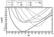
- 1 is a graph showing the change in solubility according to acidity and basic degree (pH) for various metal elements.
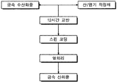
- Figure 2 is a process diagram showing the manufacturing step of the metal oxide thin film according to the present invention.
- 3A to 3C are graphs showing thin film transistor transfer characteristics according to heat treatment temperature of the zinc oxide thin film formed through Example 1 of the present invention.
- 4a to 7b are IV and CV graphs showing the performance according to the microwave oven heat treatment temperature of the ZrO x insulation layer formed in Example 1 of the present invention.
- Example 8 is a photograph showing a ZnO-based transparent thin film transistor array manufactured according to Example 1 of the present invention.
- 9A to 9D are graphs showing thin film transistor transfer characteristics according to zirconium concentration of the zirconium zinc oxide thin film formed through Example 4 of the present invention.
- 10A to 10D are graphs showing a change in performance according to time variation in applying positive bias stress according to the zirconium concentration of the zirconium zinc oxide thin film formed through Example 4 of the present invention.
- 11a to 11c are graphs showing the thin film transistor transfer characteristics according to the yttrium concentration of the yttrium zinc oxide thin film formed through the fifth embodiment of the present invention.
- 12A to 12C are graphs showing a change in performance according to a time variation in applying a positive bias stress according to the yttrium concentration of the yttrium zinc oxide thin film formed through Example 5 of the present invention.
- Example 13 is a graph comparing the change in the threshold voltage over time for the yttrium zinc oxide thin film formed through Example 5 of the present invention.
- FIG. 14 is a graph showing a change in threshold voltage with time of applying negative bias and thermal stress to the yttrium zinc oxide thin film formed through Example 5 of the present invention.
- 15A to 15C are graphs showing thin film transistor transfer characteristics according to lithium concentration of a lithium zinc oxide thin film formed through Example 6 of the present invention.
- FIG. 16 is a graph showing thin film transistor transfer characteristics of a lithium and zirconium zinc oxide thin film formed through Example 7 of the present invention.
- FIG. 17 is a graph showing a change in performance according to a change in time for applying a positive bias stress of a lithium and zirconium zinc oxide thin film formed through Example 7 of the present invention.
- Embodiments of the present invention can express semiconductor, insulator and conductor characteristics through low temperature process by using metal hydroxide which is close to oxide as a starting material and does not generate residual organic matter when forming thin film by solution method.
- metal hydroxide which is close to oxide as a starting material and does not generate residual organic matter when forming thin film by solution method.
- a transparent oxide thin film and a method of forming the same are proposed.
- metal hydroxide aluminum hydroxide (Al (OH) 3 ), zinc hydroxide (Zn (OH) 2 ), gallium hydroxide (Ga (OH) 3 ), indium hydroxide (In (OH) 3 ) ), Tin hydroxide (Sn (OH) 4 ) or a combination thereof may be used.
- metal hydroxide for semiconductor may be included in a concentration of 0.05 to 40 mol / L, a concentration of 0.05 to 20 mol / L, a concentration of 0.05 to 10 mol / L.
- Yttrium, zirconium, hafnium, scandium, gallium, lanthanum, or a combination thereof may be added for bias and / or temperature stability of the semiconductor thin film.
- Positive bias stress and negative bias of oxide semiconductor thin film, performance instability with temperature (change of threshold voltage according to voltage application and heat) are alleviated by the addition of these elements yttrium, zirconium, hafnium, scandium, gallium, lanthanum It can be removed to express a stable semiconductor characteristics.
- lithium, titanium, or a combination thereof may be added for high performance of the semiconductor thin film. Due to their addition, high performance semiconductor devices can be manufactured.
- metal elements elements for stabilization: Y, Zr, Hf, Sc, Ga, La
- elements for improving performance: Li, Ti a semiconductor capable of producing stable and high performance can be produced.
- These two kinds of elements are the above-mentioned aluminum hydroxide (Al (OH) 3 ), zinc hydroxide (Zn (OH) 2 ), gallium hydroxide (Ga (OH) 3 ), indium hydroxide (In (OH) 3 ), tin hydroxide (Sn (OH) 4 ) may be included as a mole number of 0 to 2, 0 to 20 compared to 100 moles of metal hydroxide for semiconductors. For example, precipitation may occur when the number of moles of zinc is greater than 20, compared to 100 moles of zinc hydroxide.
- Yttrium, zirconium, hafnium, scandium, gallium, lanthanum elements may be added in hydroxide form.
- Yttrium hydroxide (Y (OH) 3 ), zirconium hydroxide (Zr (OH) 4 ), hafnium hydroxide (Hf (OH) 4 ), scandium hydroxide (Sc (OH) 3 ), gallium hydroxide (Ga ( OH) 3 ) and lanthanum hydroxide (La (OH) 3 ) are more effective in the Y, Zr, Hf, Sc, Ga, and La elements, which can cause relatively strong ion defects with oxygen than the Zn, Sn, and In elements.
- the semiconductor film is stabilized and is not significantly influenced by positive, negative bias and heat stress, so that the gate voltage is applied for a long time, or the effect of changing the threshold voltage even in the case of repeated application or heat application is greatly reduced.
- the inventors also confirmed that lithium hydroxide Li (OH) and titanium hydroxide (Ti (OH)) increase the number of electron carriers when a certain amount of Li and Ti metal elements are added to improve the performance.
- zirconium hydroxide (Zr (OH) 4 ), hafnium hydroxide (Hf (OH) 4 ), aluminum hydroxide (Al (OH) 3 ), yttrium hydroxide (Y (OH) 3 ), gadolinium hydroxide (Gd (OH) 3 ), lanthanum hydroxide (La (OH) 3 ) or a combination thereof may be used.
- zinc hydroxide (Zn (OH) 2 ), indium hydroxide (In (OH) 3 ), tin hydroxide (Sn (OH) 4 ), aluminum hydroxide (Al (OH) 3 ) or Combinations of these can be used.
- the inventors of the present invention can dissolve most of the metal hydroxide corresponding to the oxide required in the transparent electronic device without an additional stabilizer under acidic or basic conditions, and the thin film prepared therefrom is, for example, at a low temperature of 200 ° C to 250 ° C. It was confirmed that the change to the corresponding oxide at °C.
- the metal hydroxide in order to enable such a change reaction at a cryogenic temperature (about 140 ° C.), by using microwave heat treatment, the metal hydroxide can selectively and effectively absorb microwave energy to promote the change into the oxide.
- a cryogenic temperature about 140 ° C.
- a thin film expressing semiconducting, insulating, and conductive properties can be prepared by directly using a high purity metal hydroxide as a starting material without undergoing a precipitation process from a metal salt.
- an oxide film starting from a complex material such as a metal salt, metal alkoxide, or metal-organic compound used in a solution process the thin film formation process and steps are complicated.
- metals, salts and alkoxides attached thereto they are reacted through sol-gel reactions through hydrolysis and condensation processes. It may act as an impeding factor or impede the electrical properties, which can be removed only by the high temperature heat treatment, resulting in the formation of an oxide thin film exhibiting device performance only through the high temperature heat treatment.
- the metal hydroxide which is a starting material proposed in the present invention can be dissolved at an appropriate pH condition, and can be dissolved in a thin film only through pyrolysis and dehydroxylation at low temperature without complicated multi-step reaction such as desorption and decomposition of additional organic materials. It is possible to form a high quality oxide film without impurities such as organic matter or anion remaining.
- Appropriate acid group titrants can be used to dissolve metal hydroxides without the need for a separate stabilizer.
- the acid group titrant may be included, for example, at a concentration of 0.05 to 40 mol / L.
- ammonia tetramethyl ammonium hydroxide, methylamine, urea, acetic acid, hydrochloric acid, nitric acid, sulfuric acid, hydrogen peroxide, or a combination thereof can be used.
- these precursors effectively increase the mobility of atoms in the material from the microwave, thereby promoting the dehydration reaction, removing impurities, and improving crystallinity.
- the reaction completion is more efficient than in the heat treatment method, and improved performance can be achieved at low temperatures.
- FIG. 2 shows a step of manufacturing a metal oxide thin film according to the present invention.
- the metal hydroxide is dissolved in an aqueous or non-aqueous solvent containing an acid / base titrant and stabilized through stirring to prepare a precursor solution for the metal oxide thin film.
- a zinc oxide (ZnO) thin film can be obtained using zinc hydroxide as a starting material of a semiconducting thin film, and an aluminum hydroxide, gallium hydroxide, indium hydroxide, tin hydroxide, or a combination thereof is used as a starting material.
- Aluminum-zinc oxide (AZO), tin-zinc oxide (ZTO), gallium-tin-zinc oxide (GSZO), indium-zinc oxide (IZO) thin films, and the like can be obtained.
- yttrium hydroxide (Y (OH) 3 ), zirconium hydroxide (Zr (OH) 4 ), hafnium hydroxide (Hf (OH) 4 ), scandium hydroxide (Sc (OH) 3 ), gallium hydroxide ( Thin films of ZrZnO, YZnO, GaZnO, ScZnO, HfZnO, LaZnO and the like can be obtained using Ga (OH) 3 ), lanthanum hydroxide (La (OH) 3 ), or a combination thereof.
- LiZnO and TiZnO thin films can be obtained using lithium hydroxide Li (OH), titanium hydroxide Ti (OH) or a combination thereof.
- a thin film of LiZrZnO, LiYZnO, LiGaZnO, LiScZnO, LiHfZnO, or LiLaZnO may be obtained using a combination of the above-described metal hydroxide for improving stability and metal hydroxide for improving performance in order to obtain a high performance and high stability thin film.
- zirconia zirconia (ZrO 2 ), hafnia (HfO 2 ), alumina (Al 2 O 3 ) made of zirconium hydroxide, hafnium hydroxide, aluminum hydroxide, lanthanum hydroxide, gadolinium hydroxide, yttrium hydroxide, etc. ), Lanthanum (La 2 O 3 ), gadolia (Gd 2 O 3 ), yttria (Y 2 O 3 ) thin film.
- ITO indium tin oxide
- I 2 O 3 indium oxide
- SnO 2 tin oxide
- zinc oxide through indium hydroxide, tin hydroxide, zinc hydroxide, aluminum hydroxide or a combination thereof
- Aluminum oxide (AlZnO) thin films can be fabricated.
- the acid group titrant mixed to improve the solubility of the metal hydroxide may vary depending on the metal hydroxide used. Specifically, ammonia, tetra methyl ammonium hydroxide, methylamine, urea, acetic acid, hydrochloric acid, nitric acid, sulfuric acid, hydrogen peroxide and the like may be used as the acid group titrant, but are not necessarily limited to these materials. A more effective titrant may form a complex with dissolved metal ions to increase the solubility, and the more capable of being decomposed at low temperature, the better properties can be expressed.
- the acid group titrant may be included, for example, at a concentration of 0.05 to 40 mol / L.
- the stirring step can last 12 hours or longer.
- the stirred solution forms a thin film or patterned film on the substrate through spin coating or inkjet printing or the like.
- a microwave heat treatment is performed to change the metal hydroxide into a metal oxide.
- Heat treatment step in the embodiment of the present invention was maintained in the microwave oven heat treatment output 2KW, frequency: 2.45GHz, the heat treatment temperature range of 100 ⁇ 400 °C, the heat treatment atmosphere was maintained in a vacuum or reducing atmosphere.
- Microwave heat treatment can accelerate the phase change reaction through time and selective heating than conventional heat treatment, so it can be processed short time at low temperature, and efficient heat treatment of various methods such as continuous microwave heat treatment and microwave heat treatment by pulse method Can be converted in a manner.
- the obtained oxide thin film can be subsequently added secondary annealing in various atmosphere conditions at a temperature of 100 ⁇ 300 °C as needed.
- the solution in which the metal hydroxide is dissolved may use an aqueous solvent or a non-aqueous solvent.
- Aqueous veins may be used alone or in admixture with water, and ammonia, tetramethyl ammonium hydroxide, methylamine, urea, acetic acid, hydrochloric acid, nitric acid, sulfuric acid, aqueous hydrogen peroxide solution, or a combination thereof may be used.
- the aqueous solvent may be used alone or in a mixed state with water, and an aqueous ammonia solution, an aqueous hydrogen peroxide solution, or the like, or a combination thereof may be used.
- the non-aqueous organic solvent may be used alone or in admixture with water, for example n-butyl acetate.
- 2-methoxy-1-methylethylacetate (PGMEA), 1-methoxy-2-propanol (PGME), 1-propanol , 1-butanol and the like can be used.
- the characteristics of the oxide thin film and its utility as a semiconductor, an insulator, and a conductor according to the present invention will be described in detail through specific examples.
- Zinc hydroxide Zn (OH) 2
- the precursor was highly soluble in basic so that the zinc hydroxide was dissolved in an aqueous ammonia solution and then stirred at room temperature for 12 hours to prepare a semiconducting solution.
- the solution was spin coated onto a substrate to prepare a thin film, which was then heat treated using a conventional heat treatment and microwave oven. Since zinc hydroxide dehydration occurs at about 120 ° C., it is possible to express semiconductor performance at 120 ° C. or higher.
- the microwave oven has made it possible to realize oxide thin film transistors having excellent semiconductor characteristics at the same temperature than conventional heat treatment methods.
- a thin film transistor having a bottom gate / top contact structure was formed using the zinc oxide thin film obtained after the heat treatment.
- 3A to 3C are thin film transistor transfer characteristics of a zinc oxide (ZnO) thin film formed through Example 1 (FIG. 3A: 140 ° C, FIG. 3B: 220 ° C, and 3C: 320 ° C). This is a graph.
- ZnO zinc oxide
- Each graph is spin-coated Zn (OH) 2 solution dissolved in ammonia water and heat-treated by microwave oven at different heat treatment temperatures, while changing V g from -40V to 40V while maintaining V d at a constant value of 20V. It is a measurement of the transmission characteristics. Specific device characteristic values are shown in Table 1 below. The device characteristic values are the best performance at the lowest temperatures based on the results reported in the paper so far.
- Zirconium hydroxide (Zr (OH) 4 ) was used as a starting material, and since the precursor has high solubility in basic, the dielectric solution was prepared by dissolving zirconium hydroxide in an aqueous ammonia solution and stirring at room temperature for 12 hours. The solution was spin coated onto a substrate to prepare a thin film, which was then heat treated using a conventional heat treatment and microwave oven. It was found that insulation properties were expressed at 250 ° C or higher. The microwave oven has made it possible to realize an oxide thin film having excellent insulation properties at the same temperature than the conventional heat treatment method.
- 4A-7A and 4B-7B are microwave oven heat treatment temperatures (FIGS. 4A, 4B: 250 ° C, 5A, 5B: 300 ° C, 6A, 6B: 350 ° C, and 7A, 7B: 400 ° C).
- IV and CV graphs showing the performance of the ZrO x insulating layer.
- dielectric properties (insulation strength, dielectric constant) of the zirconium oxide thin film according to the heat treatment temperature were measured and shown in Table 2.
- Dielectric strength (MV / cm) Dielectric constant Dielectric constant (K) 250 °C 0.56 9.97 300 °C 0.98 9.8 350 °C 1.39 11.0 400 °C 1.68 9.2
- ITO or AZO electrode material prepared by the solution method using a metal hydroxide starting material on a PES (Polyethersulfone) substrate or a glass substrate by spin coating, and then using a zirconium hydroxide (Zr (OH) 4 ) as a starting material
- Zr (OH) 4 zirconium hydroxide
- a dielectric solution was prepared by the method and applied by spin coating to form a ZrO x dielectric film. Depart Zn (OH) 2 on it
- the solution prepared as a material was applied by spin coating, then heat-treated at 140 ° C., and finally, the ITO or AZO solution was patterned, or the aluminum electrode was deposited by evaporation. A transparent flexible device formed through the above was produced.
- FIG. 8 is a photograph showing a ZnO-based transparent thin film transistor array fabricated according to the present embodiment, and it is possible to fabricate a device capable of expressing electrical characteristics comparable to that of a transparent, conventional vacuum deposition crystalline Si-based device on a flexible PES substrate. Confirmed.
- Zinc hydroxide (Zn (OH) 2 ) and zirconium hydroxide (Zr (OH) 4 ) were used as starting materials. Since this precursor is basic in solubility, in order to further improve stability after dissolving zinc hydroxide in aqueous ammonia solution Zirconium hydroxide was dissolved at varying concentrations. At this time, the molar ratio (atomic ratio) of zinc and zirconium was such that the mole number of the zirconium precursor was 0, 0.5, 1, 2 when the number of moles of the zinc precursor was 100. That is, the ratio of the number of atoms of zinc to zirconium was 1: 0, 1: 0.005, 1: 0.01, 1: 0.02.
- the washed substrate was dried with an IR-Lamp for 30 minutes to remove moisture, and then irradiated with UV-Lamp for 1 hour to modify the surface to be hydrophilic.
- the solution was spin coated onto a substrate to prepare a thin film, and then heat-treated using a hot plate. Dehydration of zinc hydroxide occurs at about 120 ° C., and dehydration of zirconium hydroxide occurs at about 250 ° C., so that semiconductor performance can be expressed above 250 ° C.
- the addition of zirconium hydroxide has made it possible to realize oxide thin film transistors having superior bias stability at the same temperature than semiconductors manufactured using only pure zinc hydroxide.
- a thin film transistor having a bottom gate / top contact structure was formed using a zirconium zinc oxide thin film obtained after the heat treatment.
- FIG. 9A to 9D are added by changing the molar concentration of the zirconium metal element of the zirconium oxide (ZrZnO) thin film formed through Example 4 (Fig. 9A: 0%, Fig. 9B: 0.5%, Fig. 9C: 1%, Fig. 9d: 2%) A graph showing a transfer curve of a thin film transistor.
- ZrZnO zirconium metal element of the zirconium oxide
- the gate voltage was applied to the ZnO semiconductor film prepared in Example 4 and the ZrZnO composition semiconductor film prepared by adding the Zr element for 500 seconds, and the change in device performance according to the bias stress was shown in 10a to 10d, respectively.
- the threshold voltage does not increase significantly but shows a stable appearance.
- the threshold voltage increases as the bias stress is applied.
- Table 4 below shows a change in threshold voltage.
- the threshold voltage shows little change with little change.
- Zinc hydroxide (Zn (OH) 2 ), yttrium hydroxide (Y (OH) 3 ) were used as starting materials. Since the precursor is solubility in basic, to dissolve zinc hydroxide in aqueous ammonia solution to further improve stability Yttrium hydroxide was dissolved. At this time, the molar ratio (atomic ratio) of zinc and yttrium was such that the mole number of the zirconium precursor was 0, 0.5, 1, 2 when the mole number of the zinc precursor was 100. Thereafter, the mixture was stirred at room temperature for 12 hours to prepare a semiconducting solution.
- the substrate was treated by the same experimental method as described in Example 4, and then the solution was spin coated onto the substrate to prepare a thin film, which was then heat treated using a hot plate.
- Dehydration of zinc hydroxide occurs at about 120 ° C. and dehydration of yttrium hydroxide occurs at about 280 ° C., so that the semiconductor performance can be expressed above 300 ° C.
- the addition of yttrium hydroxide has made it possible to realize oxide thin film transistors having an excellent amount of bias stability at the same temperature than semiconductors manufactured using only pure zinc hydroxide.
- the oxide thin film transistor has a high stability under negative bias and thermal stress.
- a thin film transistor having a bottom gate / top contact structure was formed using the yttrium zinc oxide thin film obtained after the heat treatment.
- 11A to 11C are thin films added by varying the yttrium metal element molar concentration of the yttrium zinc oxide (YZnO) thin film formed through Example 5 (Fig. 11a: 0.5%, Fig. 11b: 1%, and Fig. 11c: 2%) This graph shows the transfer curve of a transistor.
- YZnO yttrium zinc oxide
- the mobility of the yttrium zinc (YZnO) thin film having a yttrium elemental molar concentration of 0.5% shows a very good mobility of 1.93 cm 2 / Vs, an operating voltage of 3.9 V and a flashing ratio of 10 7 . Very good operating characteristics. Therefore, it was confirmed that a semiconductor film having excellent operating characteristics can be produced through a solution process. However, when yttrium metal ions were added, the mobility was slightly decreased, similar to the case of zirconium addition in Example 4.
- the gate voltage was applied for 500 seconds to the ZnO semiconductor film prepared in Example 2 and the YZnO-containing semiconductor film prepared by adding the Y element, and the change in device performance according to the bias stress was shown in FIGS. 12A to 12C, respectively.
- the threshold voltage did not increase significantly and showed a stable state similar to the device to which the zirconium metal element added in Example 4 was added.
- Table 7 is a table showing the amount of change in the threshold voltage, YZnO thin film, unlike the ZnO can be seen that the low value with little change in the threshold voltage, even if bias stress is applied.
- FIG. 13 is a table showing the amount of change in the threshold voltage according to the change of time.
- the threshold voltage is increased by applying a positive bias stress.
- FIGS. 14A to 14B the negative bias and thermal stress for the semiconductor films of the two compositions are applied for two hours, and the change is shown in FIGS. 14A to 14B.
- the threshold voltage is almost unchanged and stable, whereas in the case of Ynn-containing ZnO (FIG. 14A) thin film, the threshold is applied with negative bias and thermal stress. It was confirmed that the voltage dropped.
- Zinc hydroxide (Zn (OH) 2 ), Lithium hydroxide (Li (OH)) were used as starting materials. Since this precursor is basic in solubility, it is necessary to dissolve zinc hydroxide in aqueous ammonia solution to further improve mobility. Lithium hydroxide was dissolved. At this time, the molar ratio (atomic ratio) of zinc and lithium was such that the mole number of the zirconium precursor was 0, 0.5, 1, and 2 when the mole number of the zinc precursor was 100. Thereafter, the mixture was stirred at room temperature for 12 hours to prepare a semiconducting solution. After the substrate was treated as in Example 4, the solution was spin coated onto the substrate to prepare a thin film, and then heat-treated using a hot plate.
- Dehydration of zinc hydroxide occurs at about 120 ° C., and dehydration of lithium hydroxide occurs at about 300 ° C., so that semiconductor performance can be expressed at 300 ° C. or higher.
- the addition of lithium hydroxide enables the implementation of oxide thin film transistors having superior semiconductor performance at the same temperature than semiconductors manufactured using only pure zinc hydroxide.
- a thin film transistor having a bottom gate / top contact structure was formed using a lithium zinc oxide (LiZnO) thin film obtained after the heat treatment.
- LiZnO lithium zinc oxide
- FIG. 15A to 15C are thin films added by changing the molar concentration of the elemental lithium element of the lithium zinc oxide (LiZnO) thin film formed through Example 6 (FIG. 15A: 0.5%, FIG. 15B: 1%, and FIG. 15C: 2%)
- This graph shows the transfer curve of a transistor.
- Each graph is spin-coated Zn (OH) 2 , Li (OH) solution dissolved in ammonia water, heat-treated at 350 ° C using a hot plate, and V d is constant value of 20V while changing V g from -40V to 40V.
- the transfer characteristics were measured while maintaining the Specific device characteristic values are shown in Table 9 below.
- the mobility of the transistor with 1% lithium metal element molarity of lithium zinc (LiZnO) thin film showed very good results as 10.5 cm 2 / Vs, the operating voltage was 1.2 V and the flashing ratio was 10 8 . Very good operating characteristics. Therefore, it was confirmed that a semiconductor film having excellent operating characteristics can be produced through a solution process. In addition, as the lithium ions were added, the mobility and on / off current ratio increased significantly and then decreased again.
- Zinc hydroxide (Zn (OH) 2 ), zirconium hydroxide (Zr (OH) 4 , Lithium hydroxide (Li (OH)) were used as starting materials. Since these precursors are basic in solubility, zinc hydroxide was dissolved in aqueous ammonia solution. Afterwards, zirconium hydroxide was dissolved to further improve stability, and lithium hydroxide was dissolved to improve performance.
- the molar ratios of zinc, zirconium, and lithium (atomic ratios) were determined by the number of moles of zinc precursors of 100. The molar number was 1 and the molar number of the lithium precursor was 0.5, that is, the molar ratio (atomic ratio) of zinc, zirconium, and lithium was set to 1: 0.01: 0.005.
- the substrate was processed in the same manner as in Example 4.
- the solution was spin coated onto a substrate to prepare a thin film, and then heat-treated using a hot plate.
- Dehydration of zinc hydroxide occurs at about 120 ° C, dehydration at about 300 ° C for lithium hydroxide, and dehydration at about 250 ° C for zirconium hydroxide. It is possible.
- the addition of lithium and zirconium hydroxides makes it possible to realize oxide thin film transistors having superior semiconductor performance and high stability at the same temperature than semiconductors manufactured using only pure zinc hydroxide.
- FIG. 16A through 16B illustrate transfer curves of zirconium oxide and zirconium zinc (ZrLiZnO) thin films formed in Example 7 according to the addition of zirconium and lithium metal elements, according to heat treatment temperature (FIG. 16a: 350 ° C. : 300 ° C. 16C 250 ° C.) Graph.
- Each graph is spin-coated Zn (OH) 2 , Li (OH), Zr (OH) 4 solution dissolved in ammonia water and heat-treated for 2 hours at each temperature using a hot plate, and then V g from -40V to 40V.
- V d is a measurement of the transfer characteristics while maintaining a constant value of 20 V. Specific device characteristic values are shown in Table 11 below.
- the mobility of zirconium and lithium zinc (LiZnO) thin film transistors heat treated at 350 ° C is very good as 10.5 cm 2 / Vs, and the operating voltage is 1.2 V and the flashing ratio is 10 8 . Characteristics.
- Example 4 When the zirconium metal ions described above did not show a slight decrease in mobility, the results showed that the device performance increased as compared with the pure zinc oxide semiconductor as lithium ions were added.
- the gate voltage is applied to the ZnO semiconductor film made in Example 1 and the LiZrZnO composition made by adding Li and Zr elements made in Example 7 for 500 seconds to change the device performance according to the bias stress.
- 17A 350 ° C
- 17B 300 ° C
- 17C 250 ° C
- Table 12 is a table showing the amount of change in the threshold voltage. In the case of the YZnO thin film, unlike ZnO, even when bias stress is applied, it can be seen that the value of the threshold voltage shows little change.
- the threshold voltage change does not increase as much as about 4.1V, but the ZnO thin film containing lithium or zirconium is about 12V due to the bias stress. It can be seen that it shows an unstable state such as a large increase in the threshold voltage. This trend can be seen that maintained even in the case of the LiZrZnO thin film heat-treated at 300 °C.
- the metal oxide thin film according to the present invention is a thin film transistor of various structures, for example, bottom gate-bottom contact, bottom gate-top contact, top gate-top contact It can be applied to the structure of gate-top contact, top gate-bottom contact, etc., and can also be used in various electronic devices, optical devices, sensors, etc. using thin films.
- the present invention relates to a metal oxide thin film and a method for manufacturing the same, and in particular, to realize high mobility by low temperature heat treatment, excellent stability of operation and reproducibility when applying an electric field, and transparent electronic device at 350 ° C. or less to be applicable to a plastic substrate.
- the present invention can be applied to large area glass substrates, plastic substrates, flexible substrates and the like.
Landscapes
- Thin Film Transistor (AREA)
- Oxygen, Ozone, And Oxides In General (AREA)
- Liquid Deposition Of Substances Of Which Semiconductor Devices Are Composed (AREA)
- Inorganic Compounds Of Heavy Metals (AREA)
Abstract
본 발명은 수계 또는 비수계 용매에 용해된 금속수산화물과, 상기 금속수산화물의 용해도를 제어하기 위한 산염기 적정제를 포함하는 금속산화물 반도체 박막용 용액을 제공한다. 또한 다른 금속 수산화물 첨 가를 통하여 소자의 안정성을 향상 시키고, 추가 적으로 다른 금속 수산화물 첨가를 통하여 소자의 반도체적 성능을 향상 시키기 위한 용액을 합성한다. 상기 용액을 기판에 도포하고 각종 열처리 장비를 이용하여 열처리하여 저온에서 고품질의 금속산화물 박막을 얻을 수 있다. 상기 박막은 광학적으로 투명하여 각종 전자 소자용 박막이나 태양전지, 각종 센서, 메모리 소자 등에 활용될 수 있다.
Description
본 발명은 금속산화물 박막 및 그 제조 방법에 관한 것으로서, 상세하게는 저온 열처리로 투명 전자 소자를 구현할 수 있는 금속산화물 박막용 용액, 이를 이용하여 형성한 금속산화물 박막 및 그 제조 방법에 관한 것이다.
액정 표시 장치, 유기 발광 다이오드 등의 박막형 디스플레이에 대한 수요와 관심이 증가되면서, 최근에는 양질의 디바이스를 얻기 위한 노력이 급증하고 있다. 디스플레이 구동 소자로 그동안 실리콘을 기반으로 한 반도체소자 물질이 주로 연구되어 왔다.
실리콘은 물성 특성, 수명, 성능 안정성 측면에서 장점이 있는 반면, 박막을 형성하기 위해서 진공 증착과 레이저 어닐링 공정 등이 요구되며, 이를 위한 고가의 장비가 디스플레이 제작 원가를 상승시키고 있다. 이러한 관점에서 최근 금속 산화물 물질을 반도체 채널층으로 사용하는 노력이 이루어지고 있는데 금속 산화물은 투명한 소자로의 가능성을 갖고 있다.
박막 트랜지스터 소자는 기본적으로 반도체 물질, 전극 물질 그리고 유전체 물질로 이루어져 있으며, 최근에는 이 대표적인 소자의 구성 요소를 가시광 영역에서 투명한 금속 산화물을 적용하여, 투명 트랜지스터, 투명 메모리, 투명 전극 등의 신개념 소자로의 연구가 진행되고 있다. 대표적인 투명 반도체 재료로서 무기 아연산화물 (ZnO)은 에너지 밴드갭이 넓고 광투과도가 우수하여 박막 트랜지스터에서 활성 영역의 채널 층으로 이용하는데 큰 관심을 받고 있으며, 지르코니아 (ZrO2), 알루미나 (Al2O3), 실리카 (SiO2), 티타니아 (TiO2) 등은 높은 절연특성으로 인해 박막 트랜지스터에서 절연막 재료로 많이 사용되고 있다. 또한, 인듐이나 주석 같은 금속의 산화물의 경우는 투명하면서도 높은 전도도를 유지하기 때문에 트랜지스터의 전극 및 터치스크린 등 투명 전극 재료로 많은 연구가 이루어지고 있다.
그러나 우수한 특성에도 불구하고, 이러한 산화물 박막을 형성하기 위해서는 스퍼터링, 펄스 레이저 증착 (PLD) 등의 고 비용 진공 공정이 요구되는 단점이 있다. 따라서 대량 생산이 가능하고 저비용 제조 공정인 용액 기반 기술, 즉 스핀 코팅, 잉크젯 프린팅, 오프셋 프린팅, 그라비아 프린팅 등의 방법으로 박막트랜지스터를 제조하는 방법이 필요하다. 이러한 용액 공정에 사용되는 전구체 물질은 박막 트랜지스터 각각의 구성 요소에 적합한 성능, 예를 들어 반도체 물질 같은 경우는 높은 이동도와 우수한 스위칭 특성, 그리고 높은 점멸 비 (I
on
/
off ) 를 갖추어야만 하며, 절연층 같은 경우는 높은 절연능력과 적절한 유전상수를, 전극 물질의 경우는 높은 전도도와 낮은 비저항을 갖추어야 한다. 더불어 저온에서 각 구성 요소를 형성할 수 있으면서 투명도를 유지한다면 유리 이외의 투명 고분자 기판 위에서도 트랜지스터를 용액 공정으로 제조하여 유연성(flexible) 투명 트랜지스터를 구현할 수 있는 획기적인 방법을 제공할 수 있을 것이다.
특히, 350℃ 이하의 저온 열처리 하에서도 전술한 각각의 요구 특성을 발현하는 것은 고품위 소자 구현을 위하여 매우 중요하다. 그러나 용액 상태 물질을 이용하여 저온 열처리로 우수한 특성을 발현할 수 있는 산화물 박막과 이들을 조합하여 박막 트랜지스터를 제조하는 일은 용액의 조성, 코팅 후 열처리 온도 및 방법에 매우 민감하게 영향을 받게 된다. 용액은 일반적으로 금속 산화물을 구현할 수 있는 전구체 (유기 금속, 금속염 등), 이를 녹일 수 있는 용매, 용해도 향상을 위한 안정화제 (Complexing Agent) 및 기타 코팅성 및 점도 제어를 위한 첨가제로 구성된다. 사용되는 전구체의 종류에 따라 화학적 분해 반응 과정 및 반응 온도가 차이가 생기며, 그에 따라 형성되는 산화물 박막의 결정화도, 순도 등이 결정되며, 또한 안정화제 및 기타 첨가제의 종류에 따라서 유기물 분해 온도 및 잔류량이 결정된다. 일반적으로 금속-유기 화합물, 금속 알콕사이드, 금속염 등을 사용하는 졸-겔법 및 금속-유기 화합물 용액법 (Metallorganic Deposition, MOD) 의 경우는 전구체의 분해 및 산화물 생성 반응이 주로 400℃ 이상의 고온이 필요하여, 저온형 플렉서블 기판에 적용하기 어려우며, 비교적 고온에서 사용 가능한 유리 기판의 경우에도 휨 및 들뜸이 생겨서 다음 공정 진행 시에 오정렬(misalignment) 및 균열 등이 발생한다. 그래서 현재는 치밀화(pre-compaction) 공정을 통해서 반도체 공정 전 미리 열처리를 진행하지만 이런 공정 또한 추가공정이고 대형 유리 기판의 경우에는 적용하기 어려운 문제점이 있다.
종래 저온 용액 공정을 통한 산화물 반도체를 제작하기 위한 방법은 진공증착에 의한 기술이 대부분이며, 근래에 들어 졸-겔법, 콜로이드 입자법, 유기-금속 증착법 등에 대한 다수의 보고가 있었으나, 대부분 400℃ 이상의 열처리 및 후처리 공정이 필요하였다.
한편, 산화물 반도체의 경우 산화물 반도체에 첨가된 전이 금속은 환원되어 박막 내에 산소 결함과 함께 캐리어 농도를 증가시킬 수 있다. 그 결과 박막의 전도성을 높여주는 역할을 하여 이동도의 한계를 극복하는 대안이 되기도 하지만, 계속해서 양의 바이어스 스트레스(Bias stress) 를 가하게 되면, 즉 지속 적으로 양의 게이트 전압을 가해 주거나 반복적으로 전압을 가해 구동 시키면 소자의 문턱 전압이 양의 방향으로 크게 변화 되는 문제가 발생한다. 또한, 종래의 LCD, OLED 등의 디스플레이의 경우 OFF 되어 있는 소자의 경우 지속 적으로 음의 게이트 전압을 가해 주면 열이 발생 하고 이로 인해 문턱 전압이 음의 방향을 변화 되는 문제가 발생한다.
이러한 불안정한 특성은 스위칭 역할을 하는 트랜지스터로서의 안정성 측면에서 매우 큰 문제점을 가져오게 되어 실제 디바이스에 적용하기 어려운 물성을 나타낸다.
본 발명은 전술한 기술적 배경하에서 창안된 것으로, 본 발명의 목적은 바이어스 (전계) 스트레스 및 음의 전압에 의한 열 발생 스트레스에 대한 안정성이 개선된 반도체성 산화물 박막을 제공하는 것이다.
본 발명의 목적은 간단한 공정에 의하여 저온으로 형성할 수 있는 금속산화물 박막을 제공하는 것이다.
본 발명의 다른 목적은 용액 공정에 의하여 반도체 박막을 제조할 수 있는
새로운 금속산화물 박막용 용액 및 그 제조 방법을 제공하는 것이다.
본 발명의 또 다른 목적은 유연성 기판에 형성할 수 있으며 광학적으로 투명한 박막 제조 방법을 제공하는 것이다.
본 발명의 또 다른 목적은 350℃ 이하, 예를 들어 250℃ ~ 350℃ 저온 용액 공정에 의하여 박막트랜지스터 등의 전자 소자를 제조하는 방법을 제공하는 것이다.
본 발명의 또 다른 목적은 간단한 공정에 의하여 저온에서 고 성능 및 고 안정성을 발현 할 수 있는 전자 소자를 제조하는 방법을 제공 하는 것이다.
기타, 본 발명의 다른 목적 및 기술적 특징은 이하의 상세한 설명에서 더욱 구체적으로 제시될 것이다.
본 발명의 실시 예에 따른 금속 산화물 박막용 조성물은 금속수산화물; 그리고, 상기 금속수산화물의 용해도를 제어하기 위한 산염기 적정제를 포함하며, 상기 금속수산화물의 농도는 0.05 ~ 40 mol/L이다.
일 실시 예에서, 상기 산염기 적정제는 암모니아, 테트라 메틸 암모니움 수산화물, 메틸아민, 우레아, 아세트산, 염산, 질산, 황산, 과산화수소 및 이들의 조합에서 선택될 수 있다.
일 실시 예에서, 상기 금속수산화물은 알루미늄 수산화물 (Al(OH)3), 아연 수산화물 (Zn(OH)2), 갈륨 수산화물 (Ga(OH)3),인듐 수산화물 (In(OH)3), 주석 수산화물(Sn(OH)4) 및 이들을 조합한 물질 중에서 선택되는 제1 금속수산화물을 포함할 수 있다.
일 실시 예에서, 상기 금속수산화물은 알루미늄 수산화물 (Al(OH)3), 아연 수산화물 (Zn(OH)2), 갈륨 수산화물 (Ga(OH)3),인듐 수산화물 (In(OH)3), 주석 수산화물(Sn(OH)4) 및 이들을 조합한 물질 중에서 선택되는 제1 금속수산화물 및 바이어스 안정성 향상을 위해 이트륨 수산화물 (Y(OH)3), 지르코늄 수산화물 (Zr(OH)4), 하프늄 수산화물 (Hf(OH)4), 스칸듐 수산화물 (Sc(OH)3), 갈륨 수산화물 (Ga(OH)3), 란탄니움 수산화물 (La(OH)3) 및 이들을 조합한 물질 중에서 선택되는 제2 금속수산화물을 포함할 수 있다.
일 실시 예에서, 상기 제1 금속수산화물 및 상기 제2 금속수산화물은 1 : 0 ~ 0.2의 몰비로 이하로 포함될 수 있다.
일 실시 예에서 상기 제1 금속수산화물 및 상기 제2 금속수산화물은 1 : 0 ~ 0.02의 몰비로 이하로 포함될 수 있다.
일 실시 예에서, 상기 금속수산화물은 알루미늄 수산화물 (Al(OH)3), 아연 수산화물 (Zn(OH)2), 갈륨 수산화물 (Ga(OH)3),인듐 수산화물 (In(OH)3), 주석 수산화물(Sn(OH)4) 및 이들을 조합한 물질 중에서 선택되는 제1 금속수산화물, 바이어스 안정성 향상을 위해 이트륨 수산화물 (Y(OH)3), 지르코늄 수산화물 (Zr(OH)4), 하프늄 수산화물 (Hf(OH)4), 스칸듐 수산화물 (Sc(OH)3), 갈륨 수산화물 (Ga(OH)3), 란탄니움 수산화물 (La(OH)3) 및 이들을 조합한 물질 중에서 선택되는 제2 금속수산화물 및 저온에서의 성능향상을 위해 리튬 수산화물 (Li(OH), 티타늄 산화물(Ti(OH)), 및 이들을 조합한 물질 중에서 선택되는 제3 금속수산화물을 더 포함할 수 있다.
일 실시 예에서, 상기 제1 금속수산화물, 상기 제2 금속수산화물 및 상기 제3 금속수산화물은 1: 0 ~ 0.2 :0 ~ 0.2의 몰비로 포함될 수 있다.
일 실시 예에서, 상기 제1 금속수산화물, 상기 제2 금속수산화물 및 상기 제3 금속수산화물은 1: 0 ~ 0.02 :0 ~ 0.02의 몰비로 포함될 수 있다.
일 실시 예에서, 상기 금속수산화물은 알루미늄 수산화물 (Al(OH)3), 아연 수산화물 (Zn(OH)2), 갈륨 수산화물 (Ga(OH)3),인듐 수산화물 (In(OH)3), 주석 수산화물(Sn(OH)4) 및 이들을 조합한 물질 중에서 선택되는 제1 금속수산화물 및 저온에서의 성능향상을 위해 리튬 수산화물 (Li(OH), 티타늄 산화물(Ti(OH)), 및 이들을 조합한 물질 중에서 선택되는 제3 금속수산화물을 포함할 수 있다.
일 실시 예에서, 상기 제1 금속수산화물 및 상기 제3 금속수산화물은 1: 0 ~ 0.2의 몰비로 포함될 수 있다.
일 실시 예에서, 상기 제1 금속수산화물 및 상기 제3 금속수산화물은 1: 0 ~ 0.02의 몰비로 포함될 수 있다.
일 실시 예에서, 상기 금속수산화물은 지르코늄 수산화물 (Zr(OH)4), 하프늄 수산화물 (Hf(OH)4), 알루미늄 수산화물 (Al(OH)3), 이트리움 수산화물 (Y(OH)3), 가돌리늄 수산화물 (Gd(OH)3), 란탄니움 수산화물 (La(OH)3) 및 이들의 조합에서 선택되는 제4 금속수산화물을 포함할 수 있다.
본 발명의 실시 예에 따른 산화물 박막 형성 방법은 수계 또는 비수계 용매에 용해된 금속수산화물; 그리고, 상기 금속수산화물의 용해도를 제어하기 위한 산염기 적정제를 포함하는 산화물 박막용 조성물을 기판에 도포하는 단계; 그리고, 상기 조성물이 도포된 기판을 열처리하는 단계를 포함한다.
일 실시 예에서, 상기 열처리는 100℃ ~ 350℃의 범위에서 진공 또는 환원 분위기 하에서 수행될 수 있다.
일 실시 예에서, 상기 기판은 유연성 기판, 투명 기판 또는 유리기판일 수 있다.
일 실시 예에서, 상기 열처리는 핫플레이트, 컨벡션 오븐, 박스로, 또는 마이크로웨이브를 사용하여 수행될 수 있다.
본 발명의 일 실시 예에 따른 금속 산화물 박막은 수계 또는 비수계 용매에 용해된 금속수산화물; 그리고, 상기 금속수산화물의 용해도를 제어하기 위한 산염기 적정제를 포함하는 산화물 박막용 조성물을 기판에 도포하고 열처리하여 형성될 수 있다.
일 실시 예에서, 상기 기판은 유연성 기판, 투명 기판 또는 유리기판일 수 있다.
일 실시 예에서, 상기 금속 산화물 박막은 박막 트랜지스터의 활성층으로 사용될 수 있다.
본 발명의 실시 예에 따른 산화물 박막용 조성물은: 알루미늄 수산화물 (Al(OH)3), 아연 수산화물 (Zn(OH)2), 갈륨 수산화물 (Ga(OH)3),인듐 수산화물 (In(OH)3), 주석 수산화물(Sn(OH)4) 및 이들을 조합한 물질 중에서 선택되는 제1 금속수산화물; 이트륨 수산화물 (Y(OH)3), 지르코늄 수산화물 (Zr(OH)4), 하프늄 수산화물 (Hf(OH)4), 스칸듐 수산화물 (Sc(OH)3), 갈륨 수산화물 (Ga(OH)3), 란탄니움 수산화물 (La(OH)3) 및 이들을 조합한 물질 중에서 선택되는 제2 금속수산화물; 리튬 수산화물 (Li(OH), 티타늄 산화물(Ti(OH)), 및 이들을 조합한 물질 중에서 선택되는 제3 금속수산화물; 그리고 상기 금속수산화물들의 용해도를 제어하기 위한 산염기 적정제를 포함하며, 상기 금속수산화물들의 전체 농도는 0.05 ~ 10 mol/L인 것을 특징으로 한다.
일 실시 예에서, 상기 제1 금속수산화물, 상기 제2 금속수산화물 및 상기 제3 금속수산화물은 1 : 0 ~ 0.2 : 0 ~ 0.2의 몰비로 포함될 수 있다.
일 실시 예에서, 상기 제1 금속수산화물, 상기 제2 금속수산화물 및 상기 제3 금속수산화물은 1 : 0 ~ 0.02 : 0 ~ 0.02의 몰비로 포함될 수 있다.
일 실시 예에서, 상기 산염기 적정제는 암모니아, 테트라 메틸 암모니움 수산화물, 메틸아민, 우레아, 아세트산, 염산, 질산, 황산, 과산화수소 및 이들의 조합에서 선택될 수 있다.
본 발명의 실시 예에 따른 금속 산화물 박막은: 알루미늄, 아연, 갈륨, 인듐, 주석 및 이들을 조합한 물질 중에서 선택되는 제1 금속; 이트륨, 지르코늄, 하프늄, 스칸듐, 갈륨, 란탄니움 및 이들을 조합한 물질 중에서 선택되는 제2 금속; 리튬, 티타늄 및 이들을 조합한 물질 중에서 선택되는 제3 금속을 포함하며, 상기 제1 금속, 제2 금속 및 제3 금속은 1: 0 ~ 0.2 : 0 ~ 0.2의 원자수의 비로 포함된다.
일 실시 예에서, 상기 제1 금속, 제2 금속 및 제3 금속은 1: 0 ~ 0.02 : 0 ~ 0.02의 원자수의 비로 포함된다.
본 발명에 따르면 금속수산화물을 이용하여 전자 소자를 구성하는 반도체, 절연체, 전도체 박막을 간단한 공정을 통하여 저온에서 형성하며, 박막 형성 방법으로 프린팅, 스피닝, 코팅 방식 등을 이용할 수 있다.
본 발명을 활용하여 박막 트랜지스터, 태양전지, 각종 센서 및 메모리 소자 등을 제조할 수 있다.
본 발명에 따르면 용액 공정만으로 각종 전자 소자의 구현이 가능하여 전자 소자 제조 비용을 크게 낮출 수 있고 특히 유연성 소자, 광학적으로 투명한 전자 소자의 구현이 가능하다.
본 발명에 따른 반도체성 산화물 박막은 전계 인가 효과로 소자 안정성 및 재현성이 떨어지는 단점을 효과적으로 보완하여 동작 안성성과 우수한 반도체 물성을 동시에 발현 가능하다.
본 발명에 따르면 Y, Zr, Hf, Sc, Ga, La 등을 첨가할 경우 음의 바이어스 전계 인가시 발생하는 열에 의한 문턱전압의 음의 방향으로 이동을 효과적으로 제어하여 고 안정성 소자를 구현하는 단점을 보완하는 우수한 반도체 소자 성능 발현이 가능하다.
또한 성능을 향상시키기 위한 금속(Li, Ti) 첨가 시 저온에서도 고성능 발현이 가능하다.
도 1은 각종 금속 원소에 대하여 산성, 염기성 정도(pH)에 따른 용해도 변화를 보인 그래프.
도 2는 본 발명에 따른 금속산화물 박막의 제조 단계를 보인 공정도.
도 3a 내지 3c는 본 발명의 실시예 1을 통해 형성한 산화아연 박막의 열처리 온도에 따른 박막트랜지스터 전달 특성을 보인 그래프.
도 4a 내지 7b는 본 발명의 실시 예1을 통해 형성한 ZrOx 절연층의 마이크로웨이브 오븐 열처리 온도에 따른 성능을 보인 I-V 및 C-V 그래프.
도 8은 본 발명의 실시예1에 따라 제작된 ZnO 기반 투명 박막트랜지스터 어레이를 보인 사진.
도 9a 내지 9d는 본 발명의 실시예 4를 통해 형성한 지르코늄 산화아연 박막의 지르코늄 농도에 따른 박막트랜지스터 전달 특성을 보인 그래프.
도 10a 내지 10d는 본 발명의 실시예 4를 통해 형성한 지르코늄 산화아연 박막의 지르코늄 농도에 따른 양의 바이어스 스트레스를 가하는 시간 변화에 따른 성능 변화를 보인 그래프.
도 11a 내지 11c는 본 발명의 실시예 5를 통해 형성한 이트륨 산화아연 박막의 이트륨 농도에 따른 박막트랜지스터 전달 특성을 보인 그래프.
도 12a 내지 12c는 본 발명의 실시예 5를 통해 형성한 이트륨 산화아연 박막의 이트륨 농도에 따른 양의 바이어스 스트레스를 가하는 시간 변화에 따른 성능 변화를 보인 그래프.
도 13은 본 발명의 실시예 5를 통해 형성한 이트륨 산화아연 박막에 대하여 시간의 경과에 따른 문턱전압이 변화를 비교한 그래프.
도 14는 본 발명의 실시예 5를 통해 형성한 이트륨 산화아연 박막에 대하여 음의 바이어스 및 열적 스트레스를 가하는 시간에 따른 문턱 전압의 변화를 나타내는 그래프.
도 15a 내지 15c는 본 발명의 실시예 6을 통해 형성한 리튬 산화아연 박막의 리튬 농도에 따른 박막트랜지스터 전달 특성을 보인 그래프.
도 16은 본 발명의 실시예 7을 통해 형성한 리튬, 지르코늄 산화아연 박막의 박막트랜지스터 전달 특성을 보인 그래프.
도 17은 본 발명의 실시예 7을 통해 형성한 리튬, 지르코늄 산화아연 박막의 양의 바이어스 스트레스를 가하는 시간 변화에 따른 성능 변화를 보인 그래프.
본 발명의 실시 예들은 용액법으로 박막을 형성할 때 출발물질로서 산화물과 가까우며 잔류 유기물이 발생하지 않는 금속수산화물(metal hydroxide)을 사용함으로써 저온 공정을 통해 반도체, 절연체, 전도체 특성을 발현할 수 있는 투명 산화물 박막 및 그 형성 방법을 제안한다.
산화물 반도체 박막을 형성하기 위해서, 금속수산화물로서, 알루미늄 수산화물 (Al(OH)3), 아연 수산화물 (Zn(OH)2), 갈륨 수산화물 (Ga(OH)3), 인듐 수산화물 (In(OH)3), 주석 수산화물(Sn(OH)4) 또는 이들의 조합이 사용될 수 있다. 이와 같은 반도체용 금속수산화물은 0.05 ~ 40 mol/L의 농도로, 0.05 ~ 20 mol/L의 농도, 0.05 ~ 10 mol/L의 농도로 포함될 수 있다.
반도체 박막의 바이어스 및/또는 온도 안정성을 위해서 이트륨, 지르코늄, 하프늄, 스칸듐, 갈륨, 란탄니움, 또는 이들의 조합이 첨가될 수 있다. 산화물 반도체 박막의 양의 바이어스 스트레스 및 음의 바이어스, 온도에 따른 성능 불안정성(전압 인가 및 열에 따른 문턱 전압의 변동)이 이들 원소 이트륨, 지르코늄, 하프늄, 스칸듐, 갈륨, 란탄니움 등의 첨가에 따라 완화 내지는 제거될 수 있어 안정적인 반도체 특성을 발현할 수 있다.
또 반도체 박막의 고성능을 위해서 리튬, 티타늄, 또는 이들의 조합이 첨가될 수 있다. 이들의 첨가로 인해 고성능 반도체 소자를 제작할 수 있다.
이 두 가지 종류의 금속 원소 (안정화 향상용 원소 : Y, Zr, Hf, Sc, Ga, La), (성능 향상용 원소 : Li, Ti) 첨가를 통해 안정적이며 고성능 발현이 가능한 반도체를 제작할 수 있다. 이들 두 종류의 원소는 전술한 알루미늄 수산화물 (Al(OH)3), 아연 수산화물 (Zn(OH)2), 갈륨 수산화물 (Ga(OH)3), 인듐 수산화물 (In(OH)3), 주석 수산화물(Sn(OH)4) 같은 반도체용 금속수산화물 몰수 100 대비 몰수 0 내지 2, 0 내지 20으로 포함될 수 있다. 예를 들어 아연 수산화물 몰수 100 대비 몰수 20을 초과하여 포함될 경우에 석출이 될 수 있다.
이트륨, 지르코늄, 하프늄, 스칸듐, 갈륨, 란탄니움 원소는 수산화물 형태로 첨가될 수 있다. 본 발명에서 제안하는 이트륨 수산화물 (Y(OH)3), 지르코늄 수산화물 (Zr(OH)4), 하프늄 수산화물 (Hf(OH)4), 스칸듐 수산화물 (Sc(OH)3), 갈륨 수산화물 (Ga(OH)3), 란탄니움 수산화물 (La(OH)3) 의 경우는 Zn, Sn, In 원소들에 비하여 산소와 비교적 강한 이온 결함을 할 수 있는 Y, Zr, Hf, Sc, Ga, La 원소에 의해 반도체 막이 안정화되어 양, 음 바이어스 및 열에 의한 스트레스에 의한 영향을 크게 받지 않아 오랜 시간 게이트 전압이 인가되거나, 반복적 인가, 열의 인가의 경우에도 문턱전압이 변화하는 효과가 크게 줄어 든다.
본 발명자들은 또한 리튬 수산화물 Li(OH),티타늄 수산화물(Ti(OH))의 경우 Li, Ti 금속 원소의 일정량 첨가 시 전자 캐리어(electron carrier) 수를 증가시켜 성능을 향상시키는 효과를 확인하였다.
한편, 절연체 박막을 형성하기 위해서 금속수산화물로서, 지르코늄 수산화물 (Zr(OH)4), 하프늄 수산화물 (Hf(OH)4), 알루미늄 수산화물 (Al(OH)3), 이트리움 수산화물 (Y(OH)3), 가돌리늄 수산화물 (Gd(OH)3), 란탄니움 수산화물 (La(OH)3) 또는 이들을 조합이 사용될 수 있다.
한편 전도체 박막을 형성하기 위해서 금속수산화물로서 아연 수산화물 (Zn(OH)2), 인듐 수산화물 (In(OH)3), 주석 수산화물 (Sn(OH)4), 알루미늄 수산화물(Al(OH)3) 또는 이들의 조합이 사용될 수 있다.
본 발명의 발명자들은 투명 전자 소자에서 필요한 산화물에 대응되는 금속수산화물 대부분은 산성 또는 염기성 조건 하에서 별도의 안정화제 없이 용해가 가능하며, 이로부터 제조한 박막은 비교적 저온에서 예를 들어 최저 200℃ ~ 250℃에서 해당 산화물로 변화가 가능함을 확인하였다.
또한 이러한 변화 반응을 극저온(약 140℃)에서 가능하도록 하기 위해서 본 발명에서는 마이크로웨이브 열처리를 이용함으로써 금속수산화물이 선택적으로 그리고 효과적으로 마이크로웨이브 에너지를 흡수하여 산화물로 변화를 촉진할 수 있었다. 그 결과, 플라스틱 기판 위에서도 유연성 투명 전자 소자를 구현할 수 있었다.
특히, 본 발명에서는, 금속염으로부터 침전 과정을 거치지 않고, 직접 고순도의 금속수산화물을 출발 물질로 하여 반도체성, 절연성, 전도성 특성을 발현하는 박막을 제조할 수 있었다.
용액 공정에서 사용하는 금속염, 금속 알콕사이드, 금속-유기 화합물과 같은 복잡한 물질을 출발 물질로 한 산화막 같은 경우, 박막 형성 과정 및 단계가 복잡하다. 금속과 그에 붙어 있는 염이나 알콕사이드 같은 경우 졸-겔 반응을 통해 가수 분해(hydrolysis), 축합(condensation) 과정을 거치면서 반응을 하게 되고, 이 과정에서 만들어지는 박막 상에 유기물이나 음이온은 산화막 형성을 방해되는 요인 또는 전기적 특성을 저해하는 불순물로 작용할 수 있으며, 이는 고온 열처리를 통해서만 제거할 수 있어 결과적으로 고온 열처리를 통해서만 소자 성능이 발현되는 산화물 박막을 형성할 수 있게 된다.
반면, 본 발명에서 제안하는 출발 물질인 금속수산화물은 적절한 pH 조건에서 용해가 가능하며, 부가적인 유기물의 탈착 및 분해 과정과 같은 복잡 다단계 반응 없이, 저온에서 열분해 및 탈수 반응(dehydroxylation)만을 통해 박막에 잔류하는 유기물이나 음이온 같은 불순물 없이 고품질의 산화막을 형성할 수 있다. 적절한 산염기 적정제를 사용하여 별도의 안정화제를 사용하지 않고서도 금속수산화물을 용해시킬 수 있다. 산염기 적정제는 예를 들어 0.05 ~ 40 mol/L의 농도로 포함될 수 있다. 산염기 적정제로는 암모니아, 테트라 메틸 암모니움 수산화물, 메틸아민, 우레아, 아세트산, 염산, 질산, 황산, 과산화수소, 또는 이들의 조합을 사용할 수 있다.
도 1은 각종 금속 원소에 대하여 산성, 염기성 정도(pH)에 따른 용해도 변화를 보인 것으로, 이러한 결과로부터 pH를 변화시켜 금속수산화물의 용해도를 제어할 수 있으며, 용액 공정을 통하여 반도체, 절연체, 전도체 특성을 나타내는 금속 산화물을 구현하는데 적용 가능한 금속 원소군을 판별할 수 있다.
또한, 마이크로웨이브 열처리(microwave annealing)를 이용하는 경우 이들 전구체는 효과적으로 마이크로웨이브로부터 물질 내의 원자의 이동성을 크게 증가시켜 탈수화 반응 촉진, 불순물제거, 결정성 향상 등을 통하여 기존의 핫플레이트 또는 오븐을 이용한 열처리 방식에서보다 매우 효율적인 반응 완결이 이루어져 향상된 성능 구현을 저온에서 달성할 수 있다.
도 2에 본 발명에 따른 금속산화물 박막의 제조 단계를 도시하였다. 금속수산화물(metal hydroxide)을 산염기 적정제(acid/base titrant)를 포함하는 수계 또는 비수계 용매에 용해시키고, 교반(stirring)을 통하여 안정화시키는 단계를 거쳐 금속 산화물 박막용 전구체 용액을 제조한다.
본 발명에 있어서 금속수산화물은 최종적인 금속 산화물에 요구되는 물성에 따라 다양한 물질이 사용될 수 있다. 예를 들어, 반도체성 박막의 출발 물질로 아연 수산화물을 사용하여 산화아연(ZnO) 박막을 얻을 수 있으며, 또한 알루미늄 수산화물, 갈륨 수산화물, 인듐 수산화물, 주석 수산화물 또는 이들을 조합한 복합 물질을 출발 물질로 사용하여 알루미늄-아연 산화물(AZO), 주석-아연 산화물(ZTO), 갈륨-주석-아연 산화물(GSZO), 인듐-아연 산화물(IZO) 박막 등을 얻을 수 있다.
또한 바이어스 안정성을 향상시키기 위해서 이트륨 수산화물 (Y(OH)3), 지르코늄 수산화물 (Zr(OH)4), 하프늄 수산화물 (Hf(OH)4), 스칸듐 수산화물 (Sc(OH)3), 갈륨 수산화물 (Ga(OH)3), 란탄니움 수산화물 (La(OH)3) 또는 이들을 조합한 물질을 사용하여 ZrZnO, YZnO, GaZnO, ScZnO, HfZnO, LaZnO 등의 박막을 얻을 수 있다.
또한, 저온에서의 이동도 등의 성능을 향상시키기 위해서 리튬 수산화물 Li(OH), 티타늄수산화물 Ti(OH) 또는 이들을 조합한 물질을 사용하여 LiZnO, TiZnO 박막을 얻을 수 있다.
또한 고성능 및 고 안정성 박막을 얻기 위해서 위에 전술한 안정성 향상을 위한 금속수산화물과 성능 향상을 위한 금속수산화물을 조합한 물질을 사용하여 LiZrZnO, LiYZnO, LiGaZnO, LiScZnO, LiHfZnO, LiLaZnO 등의 박막을 얻을 수 있다.
유전체 박막을 위해서는 지르코늄 수산화물, 하프늄 수산화물, 알루미늄 수산화물, 란탄니움 수산화물, 가돌리늄 수산화물, 이트리움 수산화물 등을 출발물질로 사용하여 만든 지르코니아 (ZrO2),하프니아 (HfO2),알루미나 (Al2O3),란탄니아 (La2O3),가돌리아 (Gd2O3),이트리아 (Y2O3)박막을 얻을 수 있다.
전극 등의 전도체 형성을 위해서는 인듐 수산화물, 주석 수산화물, 아연 수산화물, 알루미늄 수산화물 또는 이들의 조합을 통해 인듐-주석 산화물 (ITO), 인듐산화물(I2O3),주석 산화물(SnO2),아연-알루미늄 산화물 (AlZnO) 박막을 제작할 수 있다.
금속수산화물의 용해도 향상을 위해 혼합되는 산염기 적정제는 사용되는 금속수산화물에 따라 달라질 수 있다. 구체적으로, 암모니아, 테트라 메틸 암모니움 수산화물, 메틸아민, 우레아, 아세트산, 염산, 질산, 황산, 과산화수소 등을 산염기 적정제로 사용할 수 있으나 반드시 이 물질들에 한정될 필요는 없다. 보다 효과적인 적정제로는 용해된 금속이온과 착화합물(complex)을 형성하여 용해도를 높일 수 있으며, 저온에서 분해될 수 있는 것일수록 우수한 특성을 발현할 수 있다. 산염기 적정제는 예를 들어 0.05 ~ 40 mol/L의 농도로 포함될 수 있다.
교반 단계는 12 시간 혹은 그 이상으로 지속할 수 있다. 교반된 용액은 스핀 코팅 또는 잉크젯 프린팅 등을 통하여 박막 또는 패턴화된 막을 기판에 형성한다. 박막 또는 막 패턴 형성 후 금속수산화물을 금속산화물로 변화시키기 위하여 마이크로웨이브 열처리를 수행한다.
본 발명의 실시예에서 열처리 단계는 마이크로웨이브 오븐 내에서 열처리출력 2KW, 주파수: 2.45GHz 를 유지하였으며, 열처리 온도의 범위는 100 ~ 400℃, 열처리 분위기는 진공 또는 환원 분위기를 유지하였다. 마이크로웨이브 열처리는 기존의 일반적인 열처리 보다 시간 및 선택적 가열을 통하여 상변화 반응 등을 촉진할 수 있어 저온에서 단시간 처리가 가능하며, 연속적 마이크로웨이브 열처리, 펄스 방식에 의한 마이크로웨이브 열처리 등 다양한 방식의 효율적 열처리 방식으로 변환될 수 있다. 얻어진 산화물 박막은 필요에 따라 후속적으로 100 ~ 300℃ 온도에서 다양한 분위기 상태에서 2차 어닐링을 추가할 수 있다.
본 발명에 있어서, 금속수산화물이 용해되는 용액은 수계 용매 또는 비수계 용매를 사용할 수 있다.
수계 용맥는 단독 혹은 물과 혼합된 상태로 사용할 수 있으며, 암모니아, 테트라 메틸 암모니움 수산화물, 메틸아민, 우레아, 아세트산, 염산, 질산, 황산, 과산화수소 수용액, 또는 이들의 조합이 사용될 수 있다.
수계 용매는 휘발되는 온도가 다른 유기 성분이 분해 제거되는 온도보다 낮고 금속수산화물의 반응 온도보다 낮아 잔류 유기 성분으로 작용하지 않는 반면, 박막 형성 시 코팅성을 향상시키거나 박막 계면(반도체-유전체 계면)에 트랩 사이트를 형성하기 위하여 이용될 수 있다.
수계 용매는 단독 혹은 물과 혼합된 상태로 사용될 수 있으며, 암모니아 수용액, 과산화수소 수용액 등 또는 이들의 조합이 사용될 있다.
비수계 유기 용매는 단독 또는 물과 혼합한 상태로 사용할 수 있으며, 예를 들어 n-부틸아세테이트(n-Butyl acetate). 2-메톡시-1-메틸에틸아세테이트(2-methoxy-1-methylethylacetate : PGMEA), 1-메톡시-2-프로판올(1-Methoxy-2-propanol : PGME), 1-프로판올(1-Propanol), 1-부탄올(1-Butanol) 등이 이용될 수 있다.
이하에서는 구체적인 실시예를 통하여 본 발명에 따른 산화물 박막의 특성 및 반도체, 절연체, 전도체로의 활용성을 상세하게 제시한다.
실시예
1. 산화아연(
ZnO
) 반도체 박막의 제조
아연 수산화물(Zn(OH)2)출발 물질로 사용하였고, 이 전구체는 염기성에서 용해도가 높으므로 암모니아 수용액에 아연 수산화물을 용해시킨 후 상온에서 12시간 동안 교반하여 반도체성 용액을 제조하였다. 이 용액을 기판에 스핀 코팅하여 박막을 제조한 후 일반적 방식의 열처리와 마이크로웨이브 오븐을 사용하여 열처리하였다. 아연 수산화물은 약 120℃에서 탈수반응(dehydration) 이 일어나므로 120℃ 이상에서 반도체 성능의 발현이 가능하다. 마이크로웨이브 오븐은 기존 열처리 방식보다 동일한 온도에서 우수한 반도체 특성의 산화물 박막 트랜지스터를 구현 가능케 하였다.
열처리 후 얻어진 산화아연 박막을 이용하여 바텀게이트/탑컨택(bottom gate/top contact) 구조의 박막트랜지스터를 형성하였다.
도 3a 내지 3c는 실시예 1을 통해 형성한 산화아연(ZnO) 박막의 열처리 온도에 따른 (도 3a: 140℃, 도 3b: 220℃, 도 3c: 320℃) 박막트랜지스터 전달 특성(transfer curve)을 보인 그래프이다.
각 그래프는 암모니아수에 녹인 Zn(OH)2 용액을 스핀 코팅하고 마이크로웨이브 오븐을 이용하여 열처리 온도별로 열처리한 다음, Vg를 -40V 에서 40V 까지 변화시키면서 Vd는 20V의 일정한 값으로 유지한 채로 전달 특성을 측정한 것이다. 구체적인 소자 특성값은 아래의 표 1에 제시하였다. 소자 특성값은 현재까지 논문에 보고된 결과를 기준으로 할 때 최저 온도에서 최고 성능이라고 할 수 있다.
표 1
| 온도 | 140℃ | 220℃ | 320℃ |
| 이동도(cm2/Vs) | 1.75 | 2.75 | 5.72 |
| 문턱전압(Vth)(V) | 8.04 | 6.7 | 2.93 |
| 서브문턱기울기(subthreshold slope)(V/dec) | 0.74 | 0.55 | 0.86 |
| 점멸비(On/off ratio) | 107 | 107 | 107 |
실시예
2.
ZrO
x
유전체 박막의 제조
지르코늄 수산화물 (Zr(OH)4)을 출발 물질로 사용하였고, 이 전구체는 염기성에서 용해도가 높으므로 암모니아 수용액에 지르코늄 수산화물을 용해시킨 후 상온에서 12시간 동안 교반하여 유전체성 용액을 제조하였다. 이 용액을 기판에 스핀 코팅하여 박막을 제조한 후 일반적 방식의 열처리와 마이크로웨이브 오븐을 사용하여 열처리하였다. 250℃ 이상에서 절연 특성이 발현됨을 파악하였다. 마이크로웨이브 오븐은 기존 열처리 방식보다 동일한 온도에서 우수한 절연 특성의 산화물 박막을 구현 가능케 하였다.
열처리 후 얻어진 지르코늄산화물 박막에 대하여 유전 특성을 조사하였다. 도 4a 내지 7a 및 도 4b 내지 7b는 마이크로웨이브 오븐 열처리 온도에 따른 (도 4a, 4b: 250℃, 도 5a, 5b: 300℃, 도 6a, 6b: 350℃, 도 7a, 7b: 400℃) ZrOx절연층의 성능을 나타내는 I-V 및 C-V 그래프이다. 또한, 열처리 온도에 따른 지르코늄산화물 박막의 유전체 특성(절연 내력, 유전 상수)을 측정하여 표 2에 나타내었다.
표 2
| 절연내력: Dielectric strength (MV/cm) | 유전상수: Dielectric constant (K) | |
| 250℃ | 0.56 | 9.97 |
| 300℃ | 0.98 | 9.8 |
| 350℃ | 1.39 | 11.0 |
| 400℃ | 1.68 | 9.2 |
실시예
3. 전 용액 공정을 통한 투명 트랜지스터 제조
PES(Polyethersulfone) 기판 또는 유리 기판 위에 금속수산화물 출발물질을 이용하여 용액법으로 제조한 ITO 또는 AZO 전극물질을 스핀코팅으로 도포한 다음, 지르코늄 수산화물 (Zr(OH)4)을 출발물질로 이용하여 용액법으로 유전체 용액을 제조하고 스핀코팅으로 도포하여 ZrOx유전체막을 형성하였다. 그 위에 Zn(OH)2를 출발
물질로 사용하여 제조한 용액을 스핀코팅을 이용해 도포한 후 140℃에서 열처리를 한 후, 최종적으로 ITO 또는 AZO 용액을 패터닝 하거나, 또는 증발법을 이용하여 알루미늄 전극을 증착함으로써 전체 층들이 용액 공정을 통하여 형성된 투명한 유연성 소자를 제작하였다.
도 8은 본 실시예에 따라 제작된 ZnO 기반 투명 박막트랜지스터 어레이를 보인 사진이며, 유연성 PES 기판 위에서 투명하면서도 기존의 진공증착 결정질 Si 기반 소자와 필적할만한 전기적 특성을 발현할 수 있는 소자 제작이 가능함을 확인하였다.
실시예
4. 산화 지르코늄 아연(
ZrZnO
) 반도체 박막의 제조
아연 수산화물(Zn(OH)2), 지르코늄 수산화물 (Zr(OH)4) 출발 물질로 사용하였고, 이 전구체는 염기성에서 용해도가 있으므로 암모니아 수용액에 아연 수산화물을 용해시킨 후 추가 적으로 안정성을 향상 시키기 위해 지르코늄 수산화물을 농도를 변화 시키며 용해 시켰다. 이 때 아연과 지르코늄의 몰비(원자수비)는 아연 전구체의 몰수를 100이라 할 때 지르코늄 전구체의 몰수가 0, 0.5, 1, 2가 되도록 하였다. 즉 아연 대 지르코늄의 원자수의 비를 1: 0, 1: 0.005, 1: 0.01, 1: 0.02로 하였다.
그 후, 상온에서 12시간 동안 교반하여 반도체성 용액을 제조하였다. 위의 용액을 스핀코팅 하기 전에 100nm 두께의 SiO2가 형성되어 있는 과도핑 실리콘 기판(Heavily Doped Silicon Substrate)을 피라나 용액(Sulfur Acid : Hydroperoxide = 4:1)에서 5분간 초음파 처리를 통하여 세척하고, Methyl alchohol, Iso-propyl alcohol (IPA), Ethyl alcohol, DI-Water 의 순서로 같은 방법으로 세정하였다.
세척이 끝난 기판은 IR-Lamp로 30분간 건조하여 수분을 제거한 후, UV-Lamp로 UV를 1시간 조사하여 표면을 친수성으로 개질 하였다. 이 용액을 기판에 스핀 코팅하여 박막을 제조한 후 핫플레이트를 사용하여 열처리하였다. 아연 수산화물은 약 120℃에서 탈수반응(dehydration) 이 일어나고 지르코늄 수산화물의 경우 약 250℃에서 탈수 반응이 일어나므로 250℃ 이상에서 반도체 성능의 발현이 가능하다. 지르코늄 수산화물 첨가는 기존 순수한 아연 수산화물만을 이용해 제작한 반도체 보다 동일한 온도에서 우수한 바이어스 안정성을 갖는 산화물 박막 트랜지스터를 구현 가능케 하였다.
열처리 후 얻어진 산화 지르코늄 아연 박막을 이용하여 바텀게이트/탑컨택 (bottom gate/top contact) 구조의 박막트랜지스터를 형성하였다.
도 9a 내지 9d는 실시예 4를 통해 형성한 산화 지르코늄 아연(ZrZnO) 박막의 지르코늄 금속 원소 몰 농도를 변화시켜 첨가한 (도 9a: 0%, 도 9b: 0.5%, 도 9c: 1%, 도 9d: 2%) 박막트랜지스터 전달 특성(transfer curve)을 보인 그래프이다.
각 그래프는 암모니아수에 녹인 Zn(OH)2, Zr(OH)4 용액을 스핀 코팅하고 핫플레이트를 이용하여 350℃ 에서 두 시간 동안 열처리한 다음, Vg를 -40V 에서 40V 까지 변화시키면서 Vd는 20V의 일정한 값으로 유지한 채로 전달 특성을 측정한 것이다. 구체적인 소자 특성값은 아래의 표 3에 제시하였다.
표 3
| 지르코늄 도핑 몰비(dopping mol ratio) | 0% | 0.5% | 1% | 2% |
| 이동도(cm2/Vs) | 2.08 | 1.82 | 1.74 | 1.23 |
| 문턱전압(Vth)(V) | 3.7 | 4.1 | 4.5 | 7.2 |
| 점멸비(On/off ratio) | 107 | 107 | 107 | 106 |
이 성능 측정에 의하면 350℃ 제작한 순수한 산화 아연 박막 트랜지스터 의 경우 이동도가 2.08 cm2/Vs로서 매우 우수한 결과를 보이고 있고, 작동 전압이 4.1 V 이며 점멸비가 107로서 매우 우수한 동작 특성을 나타내었다. 따라서, 뛰어난 동작 특성의 반도체 막을 용액 공정을 통해서 제작 할 수 있음을 확인하였다. 다만 지르코늄 금속 이온 첨가 시 이동도가 조금 하락하는 결과를 확인 하였다.
또한, 실시예 4를 통해 만들어진 ZnO 반도체 막과 Zr 원소를 첨가하여 제작한 ZrZnO 조성의 반도체 막에 대하여 500 초 동안 게이트 전압을 걸어 주어 바이어스 스트레스에 따른 소자 성능 변화를 각각 10a 내지 10d에 도시 하였다. 지르코늄이 포함된 ZrZnO 박막의 경우 문턱 전압이 크게 상승하지 않고 안정적인 모습을 보임에 반하여, 지르코늄을 넣지 않은 ZnO 박막의 경우 바이어스 스트레스를 가함에 따라 문턱 전압이 상승하는 것을 확인할 수 있다.
아래 표 4는 문턱전압의 변화량을 나타낸 표로써, ZrZnO 박막의 경우, ZnO 와 달리 바이어스 스트레스를 가하여도, 문턱 전압의 변화가 거의 없이 낮은 수치를 나타 내는 것을 볼 수 있다.
표 4
| 지르코늄 도핑 몰비(dopping mol ratio) | 문턱전압 변화(ΔVth) |
| 0% | ~12V |
| 0.5% | ~8V |
| 1% | ~4.6V |
| 2% | ~4.8V |
또한 저온공정에서의 안정성 향상을 확인하기 위한 목적으로, ZrZnO 박막 형성이 가능한 온도인 250℃에서 제작된 트랜지스터에서 지르코늄 이온 첨가에 의해 바이어스 스트레스를 가하여도 문턱 전압의 변화량이 줄어드는지 확인하기 위하여 위와 동일한 방법으로 실험을 진행 한 결과, 표 5에서 볼 수 있듯이 문턱 전압의 변화량이 줄어들다가 포화되는 경향이 있는 것을 확인할 수 있다. 즉 지르코늄의 추가로 인해서 소자의 안정성이 향상하는 것을 확인할 수 있다.
표 5
| 지르코늄 도핑 몰비(dopping mol ratio) | 문턱전압 변화(ΔVth) |
| 0% | ~13.1V |
| 0.5% | ~9.2V |
| 1% | ~5.2V |
| 2% | ~6.7V |
실시예
5. 이트륨 도핑을 통한 고 안정성 산화 이트륨 아연(
YZnO
) 박막 반도체 박막의 제조
아연 수산화물(Zn(OH)2), 이트륨 수산화물 (Y(OH)3) 출발 물질로 사용하였고, 이 전구체는 염기성에서 용해도가 있으므로 암모니아 수용액에 아연 수산화물을 용해시킨 후 추가 적으로 안정성을 향상 시키기 위해 이트륨 수산화물을 용해 시켰다. 이 때 아연과 이트륨의 몰비(원자수비)는 아연 전구체의 몰수를 100이라 할 때 지르코늄 전구체의 몰수가 0, 0.5, 1, 2가 되도록 하였다. 그 후, 상온에서 12시간 동안 교반하여 반도체성 용액을 제조하였다. 기판을 실시예 4에 기술된 방법과 동일한 실험 방법으로 처리 한 뒤 이 용액을 기판에 스핀 코팅하여 박막을 제조한 후 핫플레이트를 사용하여 열처리하였다. 아연 수산화물은 약 120℃에서 탈수반응(dehydration) 이 일어나고 이트륨 수산화물의 경우 약 280℃에서 탈수 반응이 일어나므로 300℃ 이상에서 반도체 성능의 발현이 가능하다. 이트륨 수산화물 첨가는 기존 순수한 아연 수산화물만을 이용해 제작한 반도체 보다 동일한 온도에서 우수한 양의 바이어스 안정성을 갖는 산화물 박막 트랜지스터를 구현 가능케 하였다. 또한, 추가적으로 음의 바이어스 및 열적 스트레스 하에서 높은 안정성을 갖는 산화물 박막 트랜지스터를 구현 가능케 했다.
열처리 후 얻어진 산화 이트륨 아연 박막을 이용하여 바텀게이트/탑컨택 (bottom gate/top contact) 구조의 박막트랜지스터를 형성하였다.
도 11a 내지 11c는 실시예 5를 통해 형성한 산화 이트륨 아연(YZnO) 박막의 이트륨 금속 원소 몰 농도를 변화 시켜 첨가한 (도 11a: 0.5%, 도 11b: 1%, 도 11c: 2%) 박막트랜지스터 전달 특성(transfer curve)을 보인 그래프이다.
각 그래프는 암모니아수에 녹인 Zn(OH)2, Y(OH)3 용액을 스핀 코팅하고 핫플레이트를 350℃ 이용하여 열처리한 다음, Vg를 -40V 에서 40V 까지 변화시키면서 Vd는 20V의 일정한 값으로 유지한 채로 전달 특성을 측정한 것이다. 구체적인 소자 특성값은 아래의 표 6에 제시하였다.
이 성능 측정에 의하면 이트륨 아연(YZnO) 박막의 이트륨 금속 원소 몰 농도가 0.5%인 트랜지스터의 이동도가 1.93 cm2/Vs 로서 매우 우수한 결과를 보이고 있고, 작동 전압이 3.9 V 이며 점멸비가 107 로서 매우 우수한 동작 특성을 나타내었다. 따라서, 뛰어난 동작 특성의 반도체 막을 용액 공정을 통해서 제작할 수 있음을 확인하였다. 하지만 이트륨 금속 이온 첨가 시 실시예 4 에서의 지르코늄 첨가의 경우와 동일 하게 이동도가 조금 하락 하는 결과를 확인 하였다.
표 6
| 이트륨 도핑 몰비(mol ratio) | 0% | 0.5% | 1% | 2% |
| 이동도(cm2/Vs) | 2.08 | 1.93 | 1.81 | 1.21 |
| 문턱전압(V) | 3.7 | 3.9 | 4.1 | 8.2 |
또한, 실시예 2을 통해 만들어진 ZnO 반도체 막과 Y 원소를 첨가하여 제작한 YZnO 조성의 반도체 막에 대하여 500 초 동안 게이트 전압을 걸어 주어 바이어스 스트레스에 따른 소자 성능 변화를 각각 도 12a 내지 12c에 도시 하였다. 이트륨이 포함된 YZnO 박막의 경우 문턱 전압이 크게 상승하지 않고 실시예 4에서 진행한 지르코늄 금속 원소를 첨가한 소자 와 유사하게 안정적인 모습을 보이는 것을 확인 하였다. 표 7은 문턱전압의 변화량을 나타낸 표로써, YZnO 박막의 경우, ZnO 와 달리 바이어스 스트레스를 가하여도, 문턱 전압의 변화가 거의 없이 낮은 수치를 나타 내는 것을 볼 수 있다.
표 7
| 이트륨 도핑 몰비(dopping mol ratio) | 문턱전압 변화(ΔVth) |
| 0% | ~12V |
| 0.5% | ~4.3V |
| 1% | ~3.87V |
| 2% | ~5.98V |
또한, 저온공정에서의 안정성 향상을 확인하기 위한 목적으로, YZnO 박막 형성이 가능한 온도인 300℃에서 제작된 트랜지스터에서 이트륨 이온 첨가에 의해 바이어스 스트레스를 가하여도 문턱 전압의 변화량이 줄어드는지 확인 하기 위하여 위와 동일한 방법으로 실험을 진행 한 결과 표 8에서 볼 수 있듯이 문턱 전압 변화량이 줄어 들다가 다시 늘어나는 경향이 있음을 확인 할 수 있다. 즉, 이트륨 이온의 첨가로 소자의 안정성이 향상되는 것을 확인할 수 있다.
표 8
| 이트륨 도핑 몰비(dopping mol ratio) | 문턱전압 변화(ΔVth) |
| 0% | ~12.6V |
| 0.5% | ~6.3V |
| 1% | ~4.87V |
| 2% | ~8.1V |
도13 은 각 각 시간의 변화에 따른 문턱 전압의 변화량을 나타낸 표로써, YZnO 박막의 경우 양의 바이어스를 장시간 가하여도 문턱 전압의 변화가 거의 없이 낮은 수치를 계속 나타내는데 반해, 이트륨을 넣지 않은 ZnO 박막의 경우 양의 바이어스 스트레스를 가함에 따라 문턱 전압이 상승하는 것을 확인 할 수 있다.
또한, 두 조성의 반도체 막에 대한 음의 바이어스 및 열 적 스트레스를 두 시간 동안 가하며 그에 따른 변화를 도 14a 내지 14b 에 도시하였다. 이트륨이 포함된 YZnO(도 14b) 박막의 경우 문턱 전압이 거의 변화하지 않고 안정적인 모습을 보임에 반하여, 이트륨을 넣지 않은 ZnO(도 14a) 박막의 경우 음의 바이어스 및 열 적 스트레스를 가함에 따라 문턱 전압이 하락하는 것을 확인할 수 있었다.
실시예
6.
리륨
도핑을 통한 고성능 산화
리륨
아연(
LiZnO
) 반도체 박막의 제조
아연 수산화물(Zn(OH)2), 리륨 수산화물 (Li(OH)) 출발 물질로 사용하였고, 이 전구체는 염기성에서 용해도가 있으므로 암모니아 수용액에 아연 수산화물을 용해시킨 후 추가 적으로 이동도를 향상 시키기 위해 리튬 수산화물을 용해 시켰다. 이 때 아연과 리튬의 몰비(원자수비)는 아연 전구체의 몰수를 100이라 할 때 지르코늄 전구체의 몰수가 0, 0.5, 1, 2가 되도록 하였다. 그 후, 상온에서 12시간 동안 교반하여 반도체성 용액을 제조하였다. 기판은 실시 예 4와 같이 처리 한 뒤 이 용액을 기판에 스핀 코팅하여 박막을 제조한 후 핫플레이트를 사용하여 열처리하였다. 아연 수산화물은 약 120℃에서 탈수반응(dehydration) 이 일어나고 리튬 수산화물의 경우 약 300℃에서 탈수 반응이 일어나므로 300℃ 이상에서 반도체 성능의 발현이 가능하다. 리튬 수산화물 첨가는 기존 순수한 아연 수산화물만을 이용해 제작한 반도체 보다 동일한 온도에서 우수한 반도체적 성능을 갖는 산화물 박막 트랜지스터를 구현 가능케 하였다.
열처리 후 얻어진 산화 리튬 아연(LiZnO) 박막을 이용하여 바텀게이트/탑컨택 (bottom gate/top contact) 구조의 박막트랜지스터를 형성하였다.
도 15a 내지 15c는 실시예 6을 통해 형성한 산화 리륨 아연(LiZnO) 박막의 리륨 금속 원소 몰 농도를 변화시켜 첨가한 (도 15a: 0.5%, 도 15b: 1%, 도 15c: 2%) 박막트랜지스터 전달 특성(transfer curve)을 보인 그래프이다.
각 그래프는 암모니아수에 녹인 Zn(OH)2, Li(OH) 용액을 스핀 코팅하고 핫플레이트를 이용하여 350도에서 열처리한 다음, Vg를 -40V 에서 40V 까지 변화시키면서 Vd는 20V의 일정한 값으로 유지한 채로 전달 특성을 측정한 것이다. 구체적인 소자 특성값은 아래의 표 9에 제시하였다.
표 9
| 리튬 도핑 몰비(dopping mol ratio) | 0% | 0.5% | 1% | 2% |
| 이동도(cm2/Vs) | 2.08 | 4.7 | 10.5 | 4.68 |
| 문턱전압(Vth)(V) | 3.7 | 2.9 | 1.2 | 3.1 |
| 점멸비(On/off ratio) | 107 | 108 | 108 | 108 |
이 성능 측정에 의하면 리튬 아연(LiZnO)박막의 리튬 금속 원소 몰농도가 1%인 트랜지스터의 이동도가 10.5 cm2/Vs 로서 매우 우수한 결과를 보이고 있고, 작동 전압이 1.2 V 이며 점멸비가 108 로서 매우 우수한 동작 특성을 나타내었다. 따라서, 뛰어난 동작 특성의 반도체 막을 용액 공정을 통해서 제작 할 수 있음을 확인하였다. 또한 리튬 이온을 첨가 함에 따라 이동도 및 on/ off current ratio 가 현격히 증가하다가 다시 감소되는 결과를 확인할 수 있었다.
또한, 저온공정에서의 이동도 향상을 확인하기 위한 목적으로, LiZnO 박막 형성이 가능한 온도인 300℃에서 제작된 트랜지스터에서 리튬 이온 첨가에 의해 이동도 및 on / off current ratio 가 향상되는지를 확인하기 위하여 위와 동일한 방법으로 실험을 진행 한 결과 표 10에서 볼 수 있듯이 리튬 아연(LiZnO)박막의 리튬 금속 원소 몰농도가 1%인 트랜지스터에서 이동도 3.22 cm2/Vs, 작동 전압 11.28 V, 점멸비가 107 로서 아연(ZnO)박막 대비 우수한 결과를 보이고 있으나 350℃ 대비 그 효과가 떨어짐을 확인할 수 있다.
표 10
| 리튬 도핑 몰비(dopping mol ratio) | 0% | 0.5% | 1% | 2% |
| 이동도(cm2/Vs) | 1.87 | 2.34 | 3.22 | 2.94 |
| 문턱전압(Vth)(V) | 11.41 | 8.95 | 11.28 | 12.09 |
| 점멸비(On/off ratio) | 107 | 107 | 107 | 107 |
실시 예: 7 .
리륨
및 지르코늄 도핑을 통한
고 성능
고 안정성 산화 지르코늄, 리튬 아연(
ZrLiZnO
) 반도체 박막의 제조
아연 수산화물(Zn(OH)2), 지르코늄 수산화물(Zr(OH)4, 리륨 수산화물 (Li(OH))을 출발 물질로 사용하였고, 이들 전구체는 염기성에서 용해도가 있으므로 암모니아 수용액에 아연 수산화물을 용해시킨 후 추가 적으로 안정성을 향상시키기 위해 지르코늄 수산화물을, 성능을 향상 시키기 위해 리튬 수산화물을 용해 시켰다. 이 때 아연, 지르코늄 그리고 리튬의 몰비(원자수비)는 아연 전구체의 몰수를 100이라 할 때 지르코늄 전구체의 몰수가 1, 리튬 전구체의 몰수가 0.5가 되도록 하였다. 즉, 아연, 지르코늄 및 리튬의 몰비(원자수비)를 1: 0.01: 0.005가 되도록 하였다.
그 후, 상온에서 12시간 동안 교반하여 반도체성 용액을 제조하였다. 기판은 실시예 4 에서 제시한 방법과 동일하게 처리 하였다. 이 용액을 기판에 스핀 코팅하여 박막을 제조한 후 핫플레이트를 사용하여 열처리하였다. 아연 수산화물은 약 120℃에서 탈수반응(dehydration) 이 일어나고 리튬 수산화물의 경우 약 300℃에서 탈수 반응이 일어나며, 지르코늄 수산화물의 경우 약 250℃에서 탈수 반응이 진행 되므로, 300℃ 이상에서 반도체 성능의 발현이 가능하다. 리튬, 지르코늄 수산화물 첨가는 기존 순수한 아연 수산화물만을 이용해 제작한 반도체 보다 동일한 온도에서 우수한 반도체적 성능을 갖고 높은 안정성을 갖는 산화물 박막 트랜지스터를 구현 가능케 하였다.
저온 공정에서의 리튬 수산화물 및 지르코늄 수산화물 첨가에 의한 효과를 확인하기 위해 350℃, 300℃, 250℃ 열처리 후 얻어진 산화 리튬 아연(ZrLiZnO) 박막을 이용하여 바텀게이트/탑컨택 (bottom gate/top contact) 구조의 박막트랜지스터를 형성하였다.
도 16a 내지 16b는 실시예 7을 통해 형성한 산화 지르코늄, 리튬 아연(ZrLiZnO) 박막의 지르코늄, 리튬 금속 원소 첨가에 따른 박막트랜지스터 전달 특성(transfer curve)을 열처리 온도 별 (도 16a: 350℃ 도 16b: 300℃ 도 16c 250℃) 그래프이다. 각 그래프는 암모니아수에 녹인 Zn(OH)2, Li(OH), Zr(OH)4 용액을 스핀 코팅하고 핫플레이트를 이용하여 각각의 온도에서 2시간 열처리 한 다음, Vg를 -40V 에서 40V 까지 변화시키면서 Vd는 20V의 일정한 값으로 유지한 채로 전달 특성을 측정한 것이다. 구체적인 소자 특성값은 아래의 표 11에 제시하였다.
표 11
| 열처리 온도 | 이동도Mobility(cm2/Vs) | 문턱전압Vth(V) | 점멸비On/off ratio | |
| ZnO | 350℃ | 2.08 | 3.7 | 107 |
| ZnO | 300℃ | 1.87 | 11.41 | 107 |
| ZnO | 250℃ | 0.89 | 12.4 | 107 |
| ZrLiZnO | 350℃ | 5.69 | 1.7 | 107 |
| ZrLiZnO | 300℃ | 3.2 | 8.7 | 107 |
| ZrLiZnO | 250℃ | 2.87 | 9.8 | 107 |
이 성능 측정에 의하면 350℃에서 열처리 된 지르코늄, 리튬 아연(LiZnO)박막 트랜지스터의 이동도가 10.5 cm2/Vs 로서 매우 우수한 결과를 보이고 있고, 작동 전압이 1.2 V 이며 점멸비가 108 로서 매우 우수한 동작 특성을 나타내었다. 실시예 4 기술한 지르코늄 금속 이온 첨가 시 이동도가 조금 하락 하는 결과를 보이지 않고 리튬 이온을 첨가함에 따라 소자적 성능이 순수한 산화 아연 산화물 반도체에 비해 상승하는 성능을 보이는 결과를 확인할 수 있었다. 300℃에서 열처리 된 지르코늄, 리튬 아연(LiZnO)박막 트랜지스터의 경우 지르코늄 금속 이온 첨가에 따른 소자적 성능 저하를 리튬 금속 이온 첨가에 따라 보완하여 순수한 산화 아연 산화물 반도체에 비해 소자적 성능이 향상되는 경향은 유지되나 350℃ 대비 성능 향상 정도가 떨어짐을 확인할 수 있다.
또한, 실시예 1을 통해 만들어진 ZnO 반도체 막과 실시예 7을 통해 만들어진 Li, Zr 원소를 첨가하여 제작한 LiZrZnO 조성의 반도체 막에 대하여 500 초 동안 게이트 전압을 걸어 주어 바이어스 스트레스에 따른 소자 성능 변화를 각각 도 17a (350℃), 도 17b (300℃), 도 17c(250℃)에 도시 하였다. 표 12는 문턱전압의 변화량을 나타낸 표로써, YZnO 박막의 경우, ZnO 와 달리 바이어스 스트레스를 가하여도, 문턱 전압의 변화가 거의 없이 낮은 수치를 나타내는 것을 볼 수 있다.
표 12
| ZnO | ZrLiZnO | ZnO | ZrLiZnO | |
| 열처리 온도 | 350℃ | 350℃ | 300℃ | 300℃ |
| 문턱전압변화 | ~12V | ~4.1V | ~12.6V | ~6.1V |
리튬, 지르코늄이 포함된 350℃ 열처리된 LiZrZnO 박막의 경우 문턱 전압 변화가 4.1V 정도로 크게 상승하지 않고 안정적인 모습을 보임에 반하여 리튬, 지르코늄을 넣지 않은 ZnO 박막의 경우 바이어스 스트레스를 가함에 따라 12 V 정도로 문턱 전압이 크게 상승하는 등 불안정한 모습을 보여 주는 것을 확인할 수 있다. 이러한 경향은 300℃ 열처리 된 LiZrZnO 박막의 경우에서도 유지됨을 확인할 수 있다.
본 발명에 따른 금속산화물 박막은 다양한 구조의 박막트랜지스터, 예를 들어 바텀게이트-바텀컨택(bottom gate-bottom contact), 바텀게이트-탑컨택(bottom gate-top contact), 탑게이트-탑컨택(top gate-top contact), 탑게이트-바텀컨택(top gate-bottom contact)의 구조 등에 모두 적용할 수 있으며, 그 밖에도 박막을 이용한 여러가지 전자 소자, 광소자, 센서 등에 이용될 수 있을 것이다.
이상에서 실시예를 통하여 본 발명을 예시적으로 설명하였으나, 본 발명은 이와 같은 특정 실시예에만 한정되는 것은 아니며 본 발명에서 제시한 기술적 사상, 구체적으로는 특허청구범위에 기재된 범주 내에서 다양한 형태로 수정, 변경, 또는 개선될 수 있을 것이다.
본 발명은 금속산화물 박막 및 그 제조 방법에 관한 것으로, 상세하게는 저온 열처리로 높은 이동도를 구현 하며, 전계 인가시 동작 안정성 및 재현성이 우수하며 플라스틱 기판에 적용 가능하도록 350℃ 이하에서 투명 전자 소자를 구현할 수 있는 금속산화물 박막용 용액, 이를 이용하여 형성한 금속산화물 박막 트랜지스터 및 그 제조 방법을 제안한다.
본 발명은 대면적 유리기판, 플라스틱 기판, 플렉시블 기판 등에 적용할 수 있다.
Claims (34)
- 금속수산화물; 그리고,상기 금속수산화물의 용해도를 제어하기 위한 산염기 적정제를 포함하며,상기 금속수산화물의 농도는 0.05 ~ 40 mol/L인 것을 특징으로 하는 산화물 박막용 조성물.
- 제1항에 있어서,상기 금속수산화물은 알루미늄 수산화물 (Al(OH)3), 아연 수산화물 (Zn(OH)2), 갈륨 수산화물 (Ga(OH)3), 인듐 수산화물 (In(OH)3), 주석 수산화물(Sn(OH)4) 및 이들을 조합한 물질 중에서 선택되는 제1 금속수산화물을 포함하는 것을 특징으로 하는 산화물 박막용 조성물.
- 제2항에 있어서,상기 금속수산화물은 바이어스 안정성 향상을 위해 이트륨 수산화물 (Y(OH)3), 지르코늄 수산화물 (Zr(OH)4), 하프늄 수산화물 (Hf(OH)4), 스칸듐 수산화물 (Sc(OH)3), 갈륨 수산화물 (Ga(OH)3), 란탄니움 수산화물 (La(OH)3) 및 이들을 조합한 물질 중에서 선택되는 제2 금속수산화물을 더 포함하는 것을 특징으로 하는 산화물 박막용 조성물.
- 제3항에 있어서,상기 제1 금속수산화물 및 상기 제2 금속수산화물은 1: 0 ~ 0.2의 몰비로 포함되는 것을 특징으로 하는 산화물 박막용 조성물.
- 제4항에 있어서,상기 제1 금속수산화물 및 상기 제2 금속수산화물은 1: 0 ~ 0.02의 몰비로 포함되는 것을 특징으로 하는 산화물 박막용 조성물.
- 제3항에 있어서,상기 산염기 적정제는 암모니아, 테트라 메틸 암모니움 수산화물, 메틸아민, 우레아, 아세트산, 염산, 질산, 황산, 과산화수소 및 이들의 조합에서 선택되는 것을 특징으로 하는 산화물 박막용 조성물.
- 제3항에 있어서,상기 금속수산화물은 저온에서의 성능향상을 위해 리튬 수산화물 (Li(OH), 티타늄 산화물(Ti(OH)), 및 이들을 조합한 물질 중에서 선택되는 제3 금속수산화물을 더 포함하는 것을 특징으로 하는 산화물 박막용 조성물.
- 제7항에 있어서,상기 제1 금속수산화물, 상기 제2 금속수산화물 및 상기 제3 금속수산화물은 1: 0 ~ 0.2: 0 ~ 0.2 몰비로 포함되는 것을 특징으로 하는 산화물 박막용 조성물.
- 제8항에 있어서,상기 제1 금속수산화물은 아연 수산화물 (Zn(OH)2)인 것을 특징으로 하는 산화물 박막용 조성물.
- 제8항에 있어서,상기 산염기 적정제는 암모니아, 테트라 메틸 암모니움 수산화물, 메틸아민, 우레아, 아세트산, 염산, 질산, 황산, 과산화수소 및 이들의 조합에서 선택되는 것을 특징으로 하는 산화물 박막용 조성물.
- 제2항에 있어서,상기 산염기 적정제는 암모니아, 테트라 메틸 암모니움 수산화물, 메틸아민, 우레아, 아세트산, 염산, 질산, 황산, 과산화수소 및 이들의 조합에서 선택되는 것을 특징으로 하는 산화물 박막용 조성물.
- 제2항에 있어서,상기 금속수산화물은 저온에서의 성능향상을 위해 리튬 수산화물 (Li(OH), 티타늄 산화물(Ti(OH)), 및 이들을 조합한 물질 중에서 선택되는 제3 금속수산화물을 더 포함하는 것을 특징으로 하는 산화물 박막용 조성물.
- 제11항에 있어서,상기 제1 금속수산화물과 상기 제3 금속수산화물은 1: 0 ~ 0.2의 몰비로 포함되는 것을 특징으로 하는 산화물 박막용 조성물.
- 제13항에 있어서,상기 제1 금속수산화물과 상기 제3 금속수산화물은 1: 0 ~ 0.02의 몰비로 포함되는 것을 특징으로 하는 산화물 박막용 조성물.
- 제11항에 있어서,상기 산염기 적정제는 암모니아, 테트라 메틸 암모니움 수산화물, 메틸아민, 우레아, 아세트산, 염산, 질산, 황산, 과산화수소 및 이들의 조합에서 선택되는 것을 특징으로 하는 산화물 박막용 조성물.
- 제1항에 있어서,상기 산염기 적정제는 암모니아, 테트라 메틸 암모니움 수산화물, 메틸아민, 우레아, 아세트산, 염산, 질산, 황산, 과산화수소 및 이들의 조합에서 선택되는 것을 특징으로 하는 산화물 박막용 조성물.
- 제1항에 있어서,상기 금속수산화물은 지르코늄 수산화물 (Zr(OH)4), 하프늄 수산화물 (Hf(OH)4), 알루미늄 수산화물 (Al(OH)3), 이트리움 수산화물 (Y(OH)3), 가돌리늄 수산화물 (Gd(OH)3), 란탄니움 수산화물 (La(OH)3) 및 이들의 조합에서 선택되는 제4 금속수산화물을 포함하는 것을 특징으로 하는 산화물 박막용 조성물.
- 제17항에 있어서,상기 산염기 적정제는 암모니아, 테트라 메틸 암모니움 수산화물, 메틸아민, 우레아, 아세트산, 염산, 질산, 황산, 과산화수소 및 이들의 조합에서 선택되는 것을 특징으로 하는 산화물 박막용 조성물.
- 제1항에 있어서,상기 금속수산화물은 아연 수산화물 (Zn(OH)2), 인듐 수산화물 (In(OH)3), 주석 수산화물 (Sn(OH)4), 알루미늄 수산화물(Al(OH)3) 및 이들의 조합에서 선택되는 제5 금속수산화물을 포함하는 것을 특징으로 하는 산화물 박막용 조성물.
- 제1항의 조성물을 기판에 도포하는 단계; 그리고상기 조성물이 도포된 기판을 열처리하는 단계를 포함하는 산화물 박막 형성 방법.
- 제20항에 있어서,상기 열처리는 100℃ ~ 350℃의 범위에서 진공 또는 환원 분위기 하에서 수행되는 것을 특징으로 하는 산화물 박막 형성 방법.
- 제20항에 있어서,상기 기판은 유연성 기판, 투명 기판 또는 유리기판인 것을 특징으로 하는 산화물 박막 형성 방법.
- 제20항에 있어서,상기 열처리는 핫플레이트, 컨벡션 오븐, 박스로, 또는 마이크로웨이브를 사용하여 수행되는 것을 특징으로 하는 산화물 박막 형성 방법.
- 제1항의 조성물을 기판에 도포하고 열처리를 진행하여 형성한 금속 산화물 박막.
- 제24항에 있어서,상기 기판은 유연성 기판, 투명 기판 또는 유리기판인 것을 특징으로 하는 금속 산화물 박막.
- 제24항에 있어서,상기 금속 산화물 박막은 박막 트랜지스터의 활성층으로 사용되는 것을 특징으로 하는 금속 산화물 박막.
- 알루미늄 수산화물 (Al(OH)3), 아연 수산화물 (Zn(OH)2), 갈륨 수산화물 (Ga(OH)3),인듐 수산화물 (In(OH)3), 주석 수산화물(Sn(OH)4) 및 이들을 조합한 물질 중에서 선택되는 제1 금속수산화물;이트륨 수산화물 (Y(OH)3), 지르코늄 수산화물 (Zr(OH)4), 하프늄 수산화물 (Hf(OH)4), 스칸듐 수산화물 (Sc(OH)3), 갈륨 수산화물 (Ga(OH)3), 란탄니움 수산화물 (La(OH)3) 및 이들을 조합한 물질 중에서 선택되는 제2 금속수산화물;리튬 수산화물 (Li(OH), 티타늄 산화물(Ti(OH)), 및 이들을 조합한 물질 중에서 선택되는 제3 금속수산화물; 그리고상기 금속수산화물들의 용해도를 제어하기 위한 산염기 적정제를 포함하며,상기 금속수산화물들의 전체 농도는 0.05 ~ 10 mol/L인 것을 특징으로 하는 산화물 박막용 조성물.
- 제27항에 있어서,상기 제1 금속수산화물, 상기 제2 금속수산화물 및 상기 제3 금속수산화물은 1: 0 ~ 0.2: 0 ~ 0.2 몰비로 포함되는 산화물 박막용 조성물.
- 제28항에 있어서,상기 제1 금속수산화물, 상기 제2 금속수산화물 및 상기 제3 금속수산화물은 1: 0 ~ 0.02: 0 ~ 0.02 의 몰비로 포함되는 산화물 박막용 조성물.
- 제27항에 있어서,상기 산염기 적정제는 암모니아, 테트라 메틸 암모니움 수산화물, 메틸아민, 우레아, 아세트산, 염산, 질산, 황산, 과산화수소 및 이들의 조합에서 선택되는 것을 특징으로 하는 산화물 박막용 조성물.
- 제30항에 있어서,상기 산염기 적정제는 0.05 ~ 40 mol/L의 농도로 포함되는 것을 특징으로 하는 산화물 박막용 조성물.
- 알루미늄, 아연, 갈륨, 인듐, 주석 및 이들을 조합한 물질 중에서 선택되는 제1 금속;이트륨, 지르코늄, 하프늄, 스칸듐, 갈륨, 란탄니움 및 이들을 조합한 물질 중에서 선택되는 제2 금속;리튬, 티타늄 및 이들을 조합한 물질 중에서 선택되는 제3 금속을 포함하며,상기 제1 금속, 상기 제2 금속 및 상기 제3 금속은 1: 0 ~ 0.2 : 0 ~ 0.2의 원자수의 비로 포함되는 것을 특징으로 하는 금속 산화물 박막.
- 제32항에 있어서,상기 제1 금속, 상기 제2 금속 및 상기 제3 금속은 1: 0 ~ 0.02 : 0 ~ 00.2의 원자수의 비로 포함되는 것을 특징으로 하는 금속 산화물 박막.
- 제7항의 조성물을 기판에 도포하고 열처리하여 반도체 박막을 형성하는 단계;상기 반도체 박막 상에 제17항의 조성물을 도포하고 열처리하여 절연성 박막을 형성하는 단계; 그리고상기 절연막 상에 제19항의 조성물을 도포하고 열처리하여 도전성 박막을 형성하는 단계를 포함하는 것을 특징으로 하는 반도체 소자 형성 방법.
Priority Applications (1)
| Application Number | Priority Date | Filing Date | Title |
|---|---|---|---|
| US14/127,562 US10032923B2 (en) | 2010-03-05 | 2011-03-04 | Metal oxide thin film, method for manufacturing the same, and solution for metal oxide thin film |
Applications Claiming Priority (4)
| Application Number | Priority Date | Filing Date | Title |
|---|---|---|---|
| KR20100019634 | 2010-03-05 | ||
| KR10-2010-0019634 | 2010-03-05 | ||
| KR10-2011-0016949 | 2011-02-25 | ||
| KR1020110016949A KR101212626B1 (ko) | 2010-03-05 | 2011-02-25 | 금속산화물 박막 및 그 제조 방법, 금속산화물 박막용 용액 |
Publications (2)
| Publication Number | Publication Date |
|---|---|
| WO2011108884A2 true WO2011108884A2 (ko) | 2011-09-09 |
| WO2011108884A3 WO2011108884A3 (ko) | 2012-03-22 |
Family
ID=44542740
Family Applications (1)
| Application Number | Title | Priority Date | Filing Date |
|---|---|---|---|
| PCT/KR2011/001506 Ceased WO2011108884A2 (ko) | 2010-03-05 | 2011-03-04 | 금속산화물 박막 및 그 제조 방법, 금속산화물 박막용 용액 |
Country Status (1)
| Country | Link |
|---|---|
| WO (1) | WO2011108884A2 (ko) |
Cited By (1)
| Publication number | Priority date | Publication date | Assignee | Title |
|---|---|---|---|---|
| US20140327654A1 (en) * | 2011-12-19 | 2014-11-06 | Sharp Kabushiki Kaisha | Touch-sensor-embedded display panel, display device provided therewith, and method for driving touch-sensor-embedded display panel |
Family Cites Families (9)
| Publication number | Priority date | Publication date | Assignee | Title |
|---|---|---|---|---|
| JP2001210156A (ja) * | 1999-11-17 | 2001-08-03 | Toyo Gosei Kogyo Kk | 透明導電性酸化スズ膜形成用塗布溶液及び透明導電性酸化スズ膜の製造方法並びに透明導電性酸化スズ膜 |
| KR20020096534A (ko) * | 2001-06-20 | 2002-12-31 | 삼성에스디아이 주식회사 | 금속·인듐 주석 산화물 복합체의 제조 방법 및 이방법으로 제조된 금속·인듐 주석 산화물 복합체를포함하는 투명 도전성 조성물 |
| KR100513930B1 (ko) * | 2003-06-17 | 2005-09-09 | 한국전기연구원 | 수산화물을 이용한 리튬2차전지용 양극재료의 제조방법 |
| KR100753329B1 (ko) * | 2003-09-30 | 2007-08-29 | 닛코킨조쿠 가부시키가이샤 | 고순도 산화아연 분말 및 그 제조방법과 고순도 산화아연타겟트 및 고순도 산화아연 박막 |
| JP5233007B2 (ja) * | 2007-03-09 | 2013-07-10 | 国立大学法人東北大学 | 透明導電材用塗料および透明導電膜の製造方法 |
| JP2008248136A (ja) * | 2007-03-30 | 2008-10-16 | Toyota Motor Corp | 金属酸化物微粒子分散液の製造方法、金属酸化物微粒子分散ペーストの製造方法、樹脂組成物、及び塗料組成物 |
| KR100960808B1 (ko) * | 2008-03-27 | 2010-05-31 | 연세대학교 산학협력단 | 산화물 반도체 박막 및 그 제조 방법 |
| KR100990217B1 (ko) * | 2008-04-16 | 2010-10-29 | 한국전자통신연구원 | 산화물 반도체 박막용 조성물, 이를 채용한 전계 효과트랜지스터 및 이의 제조방법 |
| KR100891952B1 (ko) * | 2008-07-24 | 2009-04-08 | 주식회사 나노신소재 | 투명 도전막용 산화물계 타겟 및 그 제조방법, 그리고산화물계 투명 도전막 |
-
2011
- 2011-03-04 WO PCT/KR2011/001506 patent/WO2011108884A2/ko not_active Ceased
Cited By (2)
| Publication number | Priority date | Publication date | Assignee | Title |
|---|---|---|---|---|
| US20140327654A1 (en) * | 2011-12-19 | 2014-11-06 | Sharp Kabushiki Kaisha | Touch-sensor-embedded display panel, display device provided therewith, and method for driving touch-sensor-embedded display panel |
| US9513753B2 (en) * | 2011-12-19 | 2016-12-06 | Sharp Kabushiki Kaisha | Touch-sensor-embedded display panel, display device provided therewith, and method for driving touch-sensor-embedded display panel |
Also Published As
| Publication number | Publication date |
|---|---|
| WO2011108884A3 (ko) | 2012-03-22 |
Similar Documents
| Publication | Publication Date | Title |
|---|---|---|
| KR101212626B1 (ko) | 금속산화물 박막 및 그 제조 방법, 금속산화물 박막용 용액 | |
| CN101118860B (zh) | 使用水解制造氧化锌半导体 | |
| Kim et al. | Stable and high-performance indium oxide thin-film transistor by Ga doping | |
| WO2013157715A1 (ko) | 저온 공정을 이용한 산화물 박막 제조방법, 산화물 박막 및 그 전자소자 | |
| KR101284587B1 (ko) | P-형 투명 산화물 반도체, 이를 포함하는 트랜지스터 및 그 제조방법 | |
| WO2018124390A1 (ko) | 그래핀 전극을 이용한 페로브스카이트 태양전지 및 그 제조 방법 | |
| WO2022045568A1 (ko) | 텔루륨계 반도체 소자의 제조방법, 이에 의해 제조된 텔루륨계 반도체 소자 및 박막 트랜지스터 | |
| Gao et al. | High Mobility Solution-Processed Hafnium Indium Zinc Oxide TFT With an Al-Doped ${\rm ZrO} _ {2} $ Gate Dielectric | |
| Gong et al. | Solution processable high quality ZrO2 dielectric films for low operation voltage and flexible organic thin film transistor applications | |
| KR100960808B1 (ko) | 산화물 반도체 박막 및 그 제조 방법 | |
| WO2016153172A1 (ko) | 높은 전계 효과 이동도를 가지는 basno3 박막 트랜지스터 및 그의 제조 방법 | |
| Zhu et al. | Water-derived all-oxide thin-film transistors with ZrAlO x gate dielectrics and exploration in digital circuits | |
| WO2017176038A1 (ko) | Basno3 박막 및 이의 저온 제조 방법 | |
| KR101017494B1 (ko) | InZnO 박막 및 그 제조 방법 | |
| WO2011149118A1 (ko) | 액상 공정을 이용한 산화물 반도체 박막의 형성 방법, 결정화 방법, 이를 이용한 반도체 소자 형성 방법 | |
| WO2019117363A1 (ko) | 고이동도 산화물 소결체 및 이를 포함하는 박막 트랜지스터 | |
| WO2018084421A1 (ko) | 듀얼 게이트 구조를 구비하는 산화물 반도체 트랜지스터 및 그 제조방법 | |
| CN105244283B (zh) | 紫外微图形化氧化物薄膜的制备方法及薄膜晶体管 | |
| Gao et al. | Solution-processed zirconium oxide gate insulators for top gate and low operating voltage thin-film transistor | |
| WO2023106781A1 (ko) | 스피넬 단일 결정상의 izto 산화물 반도체를 구비하는 박막트랜지스터 | |
| WO2011108884A2 (ko) | 금속산화물 박막 및 그 제조 방법, 금속산화물 박막용 용액 | |
| Thomas et al. | Be-doped ZnO thin-film transistors and circuits fabricated by spray pyrolysis in air | |
| Xu et al. | Optimizing photonic annealing technique for high-k dielectric of full-solution-processed oxide thin film transistor | |
| WO2023096425A1 (ko) | 산화물 반도체, 이의 제조방법 및 이를 포함하는 반도체 소자 | |
| WO2023195761A1 (ko) | 산화물 소결체 및 이를 포함하는 박막 트랜지스터 |
Legal Events
| Date | Code | Title | Description |
|---|---|---|---|
| NENP | Non-entry into the national phase |
Ref country code: DE |
|
| 122 | Ep: pct application non-entry in european phase |
Ref document number: 11750941 Country of ref document: EP Kind code of ref document: A2 |
|
| WWE | Wipo information: entry into national phase |
Ref document number: 14127562 Country of ref document: US |