WO2011108602A1 - 照明装置およびこれを備えた液晶表示装置 - Google Patents
照明装置およびこれを備えた液晶表示装置 Download PDFInfo
- Publication number
- WO2011108602A1 WO2011108602A1 PCT/JP2011/054788 JP2011054788W WO2011108602A1 WO 2011108602 A1 WO2011108602 A1 WO 2011108602A1 JP 2011054788 W JP2011054788 W JP 2011054788W WO 2011108602 A1 WO2011108602 A1 WO 2011108602A1
- Authority
- WO
- WIPO (PCT)
- Prior art keywords
- pattern
- light source
- portions
- reflection
- light
- Prior art date
- Legal status (The legal status is an assumption and is not a legal conclusion. Google has not performed a legal analysis and makes no representation as to the accuracy of the status listed.)
- Ceased
Links
Images





Classifications
-
- G—PHYSICS
- G02—OPTICS
- G02F—OPTICAL DEVICES OR ARRANGEMENTS FOR THE CONTROL OF LIGHT BY MODIFICATION OF THE OPTICAL PROPERTIES OF THE MEDIA OF THE ELEMENTS INVOLVED THEREIN; NON-LINEAR OPTICS; FREQUENCY-CHANGING OF LIGHT; OPTICAL LOGIC ELEMENTS; OPTICAL ANALOGUE/DIGITAL CONVERTERS
- G02F1/00—Devices or arrangements for the control of the intensity, colour, phase, polarisation or direction of light arriving from an independent light source, e.g. switching, gating or modulating; Non-linear optics
- G02F1/01—Devices or arrangements for the control of the intensity, colour, phase, polarisation or direction of light arriving from an independent light source, e.g. switching, gating or modulating; Non-linear optics for the control of the intensity, phase, polarisation or colour
- G02F1/13—Devices or arrangements for the control of the intensity, colour, phase, polarisation or direction of light arriving from an independent light source, e.g. switching, gating or modulating; Non-linear optics for the control of the intensity, phase, polarisation or colour based on liquid crystals, e.g. single liquid crystal display cells
- G02F1/133—Constructional arrangements; Operation of liquid crystal cells; Circuit arrangements
- G02F1/1333—Constructional arrangements; Manufacturing methods
- G02F1/1335—Structural association of cells with optical devices, e.g. polarisers or reflectors
- G02F1/1336—Illuminating devices
- G02F1/133602—Direct backlight
- G02F1/133611—Direct backlight including means for improving the brightness uniformity
-
- G—PHYSICS
- G02—OPTICS
- G02B—OPTICAL ELEMENTS, SYSTEMS OR APPARATUS
- G02B5/00—Optical elements other than lenses
- G02B5/02—Diffusing elements; Afocal elements
- G02B5/0205—Diffusing elements; Afocal elements characterised by the diffusing properties
- G02B5/021—Diffusing elements; Afocal elements characterised by the diffusing properties the diffusion taking place at the element's surface, e.g. by means of surface roughening or microprismatic structures
- G02B5/0221—Diffusing elements; Afocal elements characterised by the diffusing properties the diffusion taking place at the element's surface, e.g. by means of surface roughening or microprismatic structures the surface having an irregular structure
-
- G—PHYSICS
- G02—OPTICS
- G02B—OPTICAL ELEMENTS, SYSTEMS OR APPARATUS
- G02B5/00—Optical elements other than lenses
- G02B5/02—Diffusing elements; Afocal elements
- G02B5/0273—Diffusing elements; Afocal elements characterized by the use
- G02B5/0278—Diffusing elements; Afocal elements characterized by the use used in transmission
Definitions
- the present invention relates to an illumination device including a light source and a liquid crystal display device including the illumination device.
- an illumination device having a partial drive function can be used as a backlight of a liquid crystal display device, thereby providing a liquid crystal display device that achieves both power saving and a high contrast ratio.
- a backlight system in which a large number of light guide plates and a large number of light sources are arranged in a plane has been proposed.
- a technique that enables uniform illumination by providing dot-shaped light attenuation means on the surface of the light guide plate according to the distance from the light source is disclosed.
- a technique is disclosed that enables uniform illumination by interspersing minute reflection portions on the surface of a diffusion layer.
- JP 2007-293339 A Japanese Patent No. 3305411 JP 2005-284283 A
- a backlight provided with dot-shaped light attenuating means does not have a structure having a diffusing function after the light attenuating means, and therefore requires a resolution that prevents the dot-shaped pattern from being visually recognized. On the other hand, it is difficult to achieve the above resolution by a general-purpose process.
- the direct type backlight has the same problem as described above. Further, since it is formed on the lower side of the diffusion plate, use a thin diffusion plate as a pattern that can be formed by a general-purpose process. Then, the pattern is visually recognized through the diffusion plate. Since the diffusion layer provided with the reflection portion and the light source are separated from each other, there is a problem that luminance unevenness occurs due to the displacement of the light source and the reflection portion when viewed from an oblique direction.
- An object of the present invention is to provide a high-quality lighting device that can achieve both thinness and power saving and has excellent luminance uniformity in a partial drive system such as local dimming, and a liquid crystal display device including the same. It is in.
- the lighting device is disposed between the plurality of light sources, the plurality of light sources, at least one diffusion layer disposed to face the plurality of light sources, and between the plurality of light sources and the diffusion layer.
- At least one semi-transmissive reflective layer 4, and the semi-transmissive reflective layer farthest from the light source has a pattern composed of a plurality of transmissive portions 10 or reflective portions 11, and this pattern is in a region close to the light source.
- Each pattern is composed of a plurality of transmissive portions in the form of holes, and is formed in a pattern composed of a plurality of reflective portions in the form of dots in the region far from the light source.
- a lighting device includes a plurality of light sources arranged two-dimensionally, at least one diffusion layer disposed to face the plurality of light sources, and the plurality of light sources and the diffusion layers. And at least one transflective layer disposed therebetween, The transflective layer farthest from the light source has a pattern composed of a plurality of transmissive portions or reflective portions, and the gap between the transflective layer and the diffusion layer farthest from the light source is D, the most from the light source. It is characterized in that the relation D ⁇ P is satisfied, where P is the maximum arrangement interval between adjacent patterns of a plurality of transmissive portions or reflective portions of the separated transflective layers.
- FIG. 1 is a cross-sectional view of a lighting device according to a first embodiment of the present invention.
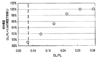
- FIG. 2 is a graph showing measured values of relative luminance when the dimension DL / PL in the lighting device is changed.
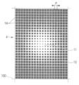
- FIG. 3 is an enlarged plan view showing an opening pattern of a transflective layer of the illumination device.
- FIG. 4 is an enlarged plan view showing an opening pattern of another transflective layer of the lighting device.
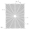
- FIG. 5 is an enlarged plan view showing an opening pattern of another transflective layer of the illumination device.
- FIG. 6 is an enlarged plan view showing an opening pattern of another transflective layer of the illumination device.
- FIG. 7 is an enlarged plan view showing an opening pattern of still another transflective layer of the illumination device.
- FIG. 1 is a cross-sectional view of a lighting device according to a first embodiment of the present invention.
- FIG. 2 is a graph showing measured values of relative luminance when the dimension DL / PL in the lighting device is changed.
- FIG. 8 is a plan view showing, in an enlarged manner, another formation pattern of the transflective layer of the illumination device, in which the formation pattern in which the aperture ratio of the transmissive reflection layer is changed from a low region to a high region is shown.
- FIG. 9 is a plan view showing still another pattern of forming a transflective layer of the lighting device, which is a rhombus-shaped array pattern.
- FIG. 10 is a plan view showing still another transflective layer formation pattern of the illumination device.
- FIG. 11A is a plan view showing luminance unevenness of a pattern pitch when the dimension D in the illumination device is zero.
- FIG. 11B is a plan view showing luminance unevenness of the pattern pitch when the dimension D in the illumination device is 3 mm.
- FIG. 12 is a graph showing the design aperture ratio (horizontal axis) of the transflective layer in the hole form for each pattern pitch P and the standard deviation (vertical axis) of the aperture ratio formed by screen printing.
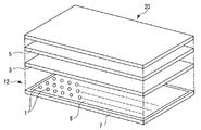
- FIG. 13 is an exploded perspective view showing a liquid crystal display device including the illumination device according to the embodiment.
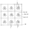
- FIG. 14 is a plan view schematically showing a light source arrangement in an illumination apparatus according to another embodiment.
- FIG. 1 is a cross-sectional view of a lighting device according to an embodiment of the present invention.
- the illumination device 12 includes, for example, a rectangular mounting board 7, a lower surface reflection layer 6 that is formed on the upper surface of the mounting board 7 and diffuses and reflects light, and the mounting board via the lower surface reflection layer 6. 7, a large number of point light sources 1, a light guide plate 3, for example, which is disposed above the point light source 1 and faces the lower reflective layer 6, and faces the light guide plate 3 with a gap.
- a rectangular diffusion sheet or diffusion plate 5 and a transflective layer 4 disposed between the light guide plate 3 and the diffusion plate 5.
- a large number of point light sources 1 composed of LEDs are arranged in a matrix over the entire surface of the mounting substrate 7 at a predetermined arrangement pitch, and are electrically connected to the mounting substrate 7.
- the peripheral edge portion of the light guide plate 3 is supported on the mounting substrate 7 by the support member 2, and the light guide plate 3 faces the lower reflective layer 6 with a predetermined gap.
- the peripheral edge of the diffusion plate 5 is supported on the light guide plate 3 by the support member 2, and the diffusion plate 5 faces the light extraction surface 4a of the light guide plate with a predetermined gap D.
- the transflective layer 4 is provided over the entire surface or a part of the light extraction surface 4 a of the light guide plate 3, that is, the surface facing the diffusion plate 5.
- the transflective layer 4 is made of a material that transmits part of light and reflects part of light.
- the light emitted from the point light source 1 enters the light guide plate 3 and propagates through the light guide plate 3, and then part of the light reaches the transflective layer 4 from the light extraction surface 4 a of the light guide plate 3.
- a part of the light passes through the transmissive part of the semi-transmissive reflective layer 4 and proceeds to the diffusion plate 5 side, and a part of the light is reflected by the reflective part of the semi-transmissive reflective layer 4 and propagates through the light guide plate 3 again. Go.
- a part of the light returning from the light guide plate 3 to the point light source 1 side is generated, but this is reflected by the lower reflective layer 6 and returned to the light guide plate 3 again.
- the dispersion of light proceeds, and the light finally emitted from the diffusion sheet or diffusion plate 5 achieves uniform brightness.
- the light emitted from a point light source such as an LED has a maximum at the upper part (center) of the light source and has a light distribution characteristic of 100 to 160 degrees in full width at half maximum. Therefore, it is necessary to increase the reflectance of the transflective layer 4 directly above the light source and reduce the amount of transmitted light.
- the degree to which light is diffused to achieve uniform brightness becomes difficult as the distance PL between point light sources increases. If the reflectance directly above the light source is increased in order to promote diffusion, the proportion of light re-entering the point light source 1 increases and the overall light utilization efficiency decreases.
- the distance DL between the transflective layer 4 and the light extraction surface (outgoing surface) of the point light source 1 is uniform. Performance and light extraction efficiency can both be achieved.
- FIG. 2 is a graph showing an actual measurement value of the average luminance of the lighting device when the distance DL between the transflective layer 4 and the light extraction surface (exit surface) of the point light source 1 is changed.
- the horizontal axis represents DL / PL
- the plurality of point light sources 1 are arranged in a lattice shape, and the arrangement interval PL is set to 15 mm, for example.
- the distance DL between the light extraction surface of the point light source 1 and the transflective layer 4 is, for example, 3 mm.
- the efficiency is ensured to be 94% or more.
- it is desirable that DP is greater than 1/8 ⁇ PL in order to ensure efficiency of 90% or more.
- FIG. 4, FIG. 5, FIG. 6, FIG. 7, FIG. 8, FIG. 9, and FIG. 10 are enlarged plan views showing opening patterns of the transflective layer 4 according to various embodiments.
- a region 100 having a repetition period of the semi-transmissive reflection layer 4 is determined in accordance with the two-dimensional arrangement of the point light sources 1, and the point light source is disposed at a position facing the center of the region 100.
- each region 100 of the transflective layer 4 is formed with a transmissive portion 10 that transmits light, and 60% or more of light in a portion where the transmissive portion 10 is not formed.
- the reflection part 11 which reflects the light and transmits 40% or less is formed.
- black portions indicate transmission holes that form the transmission portions 10, and white portions indicate reflection portions 11.
- the hole-type transflective layer 4 is configured, and a plurality of transmissive portions 10 are patterned on the reflective portion 11 at uniform intervals. Thereby, the transflective layer 4 transmits a part of the light and reflects a part of the light to form a uniform luminance distribution. That is, a pattern composed of a plurality of transmission portions 10 or reflection portions 11 is configured by combining a group of consecutive patterns having a constant pattern interval, and each pattern group is separately formed according to the formation position.
- the aperture ratio distribution is controlled by changing the size of. Or you may comprise the pattern which consists of a some permeation
- the transmissive part 10 of the semi-transmissive reflective layer 4 is configured by, for example, a rectangular transmissive hole, and is a part (end part) away from the point light source 1.
- the hole diameter of the transmission part 10 in the upper part (center part) of the point light source 1 is formed smaller than that of FIG.
- the formation interval of the transmissive portions 10 at the upper portion (center portion) of the point light source 1 is formed to be wider.
- the diffusion sheet or diffusion plate 5 is arranged such that the gap D between the transflective layer 4 and the uniform pattern interval P of the transflective layer 4 is larger. That is, the gap between the transflective layer 4 and the diffusion layer (diffusion plate 5) farthest from the light source 1 is D, and adjacent to the patterns of the plurality of transmissive portions or reflective portions of the transflective layer 4 farthest from the light source 1
- FIGS. 11A and 11B are diagrams showing luminance unevenness of the pattern pitch of the transflective layer 4 when the interval D is changed.
- values obtained by actually measuring luminance unevenness using a thin diffusion plate 5 having a thickness of 0.2 mm are shown.
- the same unevenness-improving effect can be obtained by reducing the transmittance of the diffusion plate 5 or making it thicker, but at the same time, the light component reflected and absorbed increases to reduce the efficiency, and the resin material cost and weight increase. Resulting in. Therefore, it is desirable to increase the interval D to eliminate pattern pitch unevenness.
- the aperture ratio of the transflective layer 4 is set to be low immediately above the point light source 1 and high in the surrounding area.
- the minimum aperture ratio is 10% and the maximum aperture ratio is 70% with respect to the pattern pitch P1.2 mm.
- FIG. 12 shows the designed aperture ratio (horizontal axis) of the transflective layer 4 in the hole form for each pattern pitch P and the standard deviation (variation) of the aperture ratio of the transflective layer 4 formed by screen printing (vertical axis). It is the graph which showed. From FIG. 12, it can be seen that in the high aperture ratio region, the variation in aperture ratio due to the manufacturing process increases, and in particular, the variation is large at a narrow pattern pitch P. This is because the variation in aperture ratio depends on the line width to be patterned. That is, in the hole-shaped transflective layer 4, the width of the reflective portion 11 becomes narrow in the highest aperture ratio region facing between the light sources, and variations due to the manufacturing process are likely to occur.
- the pattern pitch P is set to 1.2 mm
- the maximum aperture ratio is set to 70%.
- the distance D is set to 3 mm so that the pattern pitch unevenness is not visually recognized.
- the opening shape of the transmission hole of the transflective layer 4 is not limited to the quadrangle shown in FIG. 3, but may be other shapes such as a triangle or an ellipse, and stable formation in an existing pattern forming process such as an existing screen printing. It may be selected as appropriate in consideration of the characteristics.
- FIG. 4 shows an opening pattern of the transflective layer 4 according to the second embodiment.
- the aperture pattern has the same hole shape as in FIG. 3, but the pattern pitch P is set large at a location far from the point light source 1 and a high aperture ratio pattern is formed. Since the design aperture ratio of each pattern changes abruptly, the aperture ratio distribution is precisely controlled by reducing the pattern pitch P, and the characteristic influence due to printing variations is exerted even in a high aperture ratio region where the variations are large as shown in FIG. Designed to be difficult to get out.
- FIG. 5 shows an opening pattern of the transflective layer 4 according to the third embodiment.
- the third embodiment corresponds to a modification of the second embodiment, in which the lattice pattern arrangement is broken at the outer peripheral portion of the region 100 and the opening pattern P of the transmissive portion 10 is changed.
- FIG. 6 shows an opening pattern of the transflective layer 4 according to the fourth embodiment.
- the central region close to the point light source 1 has a hole shape
- the outer peripheral region far from the point light source has a dot shape.
- the opening pattern is formed by properly using the hole form and the dot form according to the opening ratio. That is, the opening pattern in the central area with a low aperture ratio is in the form of a hole, and the opening pattern in the peripheral area with a high aperture ratio is in the form of a dot.
- the aperture pattern distribution does not have to be symmetric with the light source directly above as the center, and an optimal distribution can be appropriately obtained in accordance with the light distribution of the light source.
- FIG. 7 shows an opening pattern of the transflective layer 4 according to the fifth embodiment.
- the opening pattern of the transflective layer 4 is a polar coordinate system, and the radial pattern interval is equal. Further, the pattern interval in the circumferential direction has a region where the aperture ratio is 50% or more and is formed at a substantially constant angle.
- the amount of light incident on the transflective layer 4 from the light source can be described by a function of radius and declination with the portion directly above the light source as the center.
- An aperture pattern having an aperture ratio distribution adapted to the distribution of the amount of light incident on the transflective layer 4 can be formed in consideration of resolution limitations in an existing pattern formation process such as screen printing.
- the pattern pitch P in the circumferential direction is increased in the outer peripheral region that requires a higher aperture ratio away from the light source, and the aperture pattern also has objectivity.
- FIG. 8 shows an opening pattern of the transflective layer 4 according to the sixth embodiment.
- the sixth embodiment corresponds to a modification of the fourth embodiment, and the opening pattern of the transflective layer 4, that is, the formation pattern, has an area close to the light source as a hole form and an outer area far from the point light source as a dot form.
- the opening pattern of the transflective layer 4 has a first direction X and a second direction Y orthogonal to the first direction X, and the aperture ratio is low along the first direction ( The pattern changes from the 0% region to the high (100%) region.
- the left end of the figure corresponds to an aperture ratio of 0%, and the right end corresponds to an aperture ratio of 100%.
- the transflective layer 4 is formed with a transmissive portion 10 that transmits light, and a reflective portion 11 that reflects 60% or more of light and transmits 40% or less of light is formed in a portion where the transmissive portion 10 is not formed. ing. That is, in this embodiment, a hole-type transflective layer 4 is formed, and a plurality of transmissive portions 10 are patterned on the reflective portion 11 at uniform intervals. Thereby, the transflective layer 4 transmits a part of the light and reflects a part of the light to form a desired light distribution.
- the pattern shape is an integrated shape in which the reflective portion 11 has no cut portion
- the transmissive portion 10 is an array shape of a plurality of patterns separated from each other.
- Each transmission part 10 is formed in a rectangular shape, for example, and the sides thereof are aligned in the first direction X and the second direction Y. While the design aperture ratio can be adjusted by changing the side length of the transmissive portion 10, if the design aperture ratio becomes too high, the side length of the transmissive portion 10 becomes too large and the formation line width of the reflective portion 11 becomes small. Too much.
- the variation in the shape of the line width increases in the region where the formation line width of the reflecting portion 11 is 100 to 200 ⁇ m, and further, the line itself cannot be formed in the region where the formation line width is 100 ⁇ m or less.
- the opening pattern of the transflective layer 4 has an integrated shape (matrix shape) in which the transmissive portion 10 has no cut portion as in the region 48b.
- the reflecting portion 11 is switched to a pattern shape that is an array shape of a plurality of patterns (for example, rectangular shapes) separated from each other.
- FIG. 9 shows an opening pattern of the transflective layer 4 according to the seventh embodiment.
- the opening pattern of the semi-transmissive reflective layer 4 has a first direction X and a second direction Y orthogonal to the first direction X, and is high from a region where the aperture ratio is low (0%) along the first direction ( 100%) pattern. That is, the area ratio of the reflecting portion changes along the first direction.
- the transmission unit 10 and the reflection unit 11 are formed in a polygonal shape, for example, a quadrangular shape or a rhombus shape, and are arranged in a direction in which diagonal directions are aligned in the second direction.
- the pattern is composed of a plurality of reflective portions 11, and each adjacent reflective portion 11 has a corner at each corner.
- the transmitting portions 10 are in contact with each other and are arranged in a pattern in which they are separated from each other.
- the pattern is composed of a plurality of transmission parts 10, and adjacent transmission parts 10 are reflected at each corner.
- the portions 11 are arranged in a pattern in which the patterns are separated from each other.
- the pattern switching unit 50 is a point where the design aperture ratio is 50%. Before and after the pattern, only the size of the pattern changes and the shape itself does not change. Therefore, the luminance unevenness in the switching unit 50 can be eliminated. By using a print pattern in which the corners are brought into contact in this way, it is possible to avoid the generation of a thin line part pattern with large variations.
- FIG. 10 shows an opening pattern of the transflective layer 4 according to the eighth embodiment.
- the opening pattern of the semi-transmissive reflective layer 4 has a first direction X and a second direction Y orthogonal to the first direction X, and is high from a region where the aperture ratio is low (0%) along the first direction ( 100%) pattern. That is, the area ratio of the reflecting portion 11 changes along the first direction.
- the transmission part 10 and the reflection part 11 are each formed in a rectangular shape, for example, and are arranged with their sides aligned in the first direction X or the second direction Y, respectively.
- the opening pattern is a pattern composed of a plurality of transmission parts 10 in the region 48a where the area ratio of the reflection part 11 is large. As the area ratio of the reflection part 11 decreases, the area of the transmission part 10 increases. It has the line part 10a which connects an adjacent permeation
- an array pattern in which a slit (line portion) is provided at the midpoint of the side of the reflecting unit 11 is used.
- the same pattern formation as that in the sixth embodiment shown in FIG. 8 is performed, and in the region 48b in which the width of the reflecting portion 11 is less than 200 ⁇ m, the side length of the transmitting portion 10 is increased. Instead, a line portion 10 a that cuts the reflecting portion 11 is provided at the midpoint of the side of the reflecting portion 11.
- the minimum width of the line portion 10a is set to 200 ⁇ m, for example, and in the region 48a where the line width is 0 to 200 ⁇ m, the side length of each transmission portion 10 is sequentially increased to increase the line portion 10a. Avoid the formation of.
- the opening pattern is formed, for example, by screen printing, a pattern shape with little variation can be obtained even when the viscosity state or printing conditions of the printing ink fluctuate, and the stable opening ratio as designed. Distribution can be obtained.
- the flat illumination unit with respect to one light source may be sufficient, and the curved-surface illuminating device like an LED light bulb may be sufficient.
- FIG. 13 is an exploded perspective view showing the liquid crystal display device.
- the liquid crystal display device includes a rectangular liquid crystal display panel 20 and an illuminating device 12 that is disposed facing the back side of the liquid crystal display panel 20 and functions as a backlight unit. Yes.
- the liquid crystal display panel 20 includes a rectangular array substrate, a rectangular counter substrate disposed to face the array substrate with a gap therebetween, and a liquid crystal layer sealed between the array substrate and the counter substrate.
- the illuminating device 12 is provided adjacent to and facing the array substrate of the liquid crystal display panel 20.
- the illuminating device 12 includes a lower surface reflection layer 6 formed on the upper surface of a rectangular mounting substrate 7, a large number of point light sources 1 arranged in a two-dimensional matrix on the mounting substrate 7, and a position above the point light source 1. And a light guide plate 3 fixed by a support member and a housing (not shown), and a diffusion sheet or diffusion plate 5 disposed between the light guide plate 3 and the liquid crystal display panel 20.
- a transflective layer 4 (not shown) is formed over the entire surface of the light extraction region.
- the opening pattern of the transflective layer 4 corresponds to the arrangement of the point light sources 1 and is formed so that the portion with a large amount of incident light from the point light source has a smaller opening ratio than other portions.
- the lighting device is configured in the same manner as the lighting device according to the above-described embodiment.
- the light emitted from the point light source 1 once propagates through the light guide plate 3, and then the transflective layer 4, the diffusion sheet, or the diffusion
- the liquid crystal display panel 20 is finally irradiated through the plate 5. After passing through the diffusion sheet or the diffusion plate 5, the light can obtain a uniform luminance distribution over the entire surface of the light extraction region.
- a lighting device that is thin, highly efficient, and has a high degree of freedom in design of luminance distribution can be obtained.
- an illuminating device having excellent luminance uniformity in the light emitting region can be obtained.
- the matrix arrangement of the point light sources 1 may be an arrangement in which a plurality of point light sources constitute one group and each group forms a matrix arrangement. However, it is preferable that the single light source is arranged in a matrix arrangement because the degree of luminance unevenness with respect to the positional deviation between the transflective layer 4 and the point light source 1 is small.
- the point light source 1 can be applied in white or other colors, and the type of the point light source 1 is not limited.
- the illumination device for the liquid crystal display panel may be an illumination device that creates white light by combining a plurality of single color LEDs.
- three LEDs emitting red, blue, and green can be adjacent to each other as one group, and a plurality of groups can be arranged in a matrix.
- the pattern of the transflective layer 4 is arranged so that the region 100 of the repetition period coincides with the boundary of the matrix arrangement period of each LED group. This makes it possible to achieve illumination with uniform brightness and chromaticity while using a multicolor light source.
- the present invention is not limited to the above-described embodiment as it is, and can be embodied by modifying the constituent elements without departing from the scope of the invention in the implementation stage.
- various inventions can be formed by appropriately combining a plurality of components disclosed in the embodiment. For example, some components may be deleted from all the components shown in the embodiment.
- constituent elements over different embodiments may be appropriately combined.
- the illuminating device as the backlight of the liquid crystal display device has been described.
- the illuminating device according to the present invention can also be used as the illuminating device itself for lighting purposes.
- the light source is not limited to a point light source, and other light sources such as a line light source may be used.
- the lighting device includes a single transflective layer and a single diffusion layer.
- the present invention is not limited to this, and a plurality of semitransparent reflective layers may be provided as necessary.
- a configuration in which a plurality of diffusion layers are provided may be employed.
- SYMBOLS 1 Point light source, 2 ... Support frame, 3 ... Light guide plate, 4 ... Semi-transmissive reflective layer, 5 ... Diffusing plate, 6 ... bottom reflective layer, 7 ... mounting substrate, 10 ... transmissive part, 10a ... line part, 11 ... reflective part, 12 ... Lighting device, 20 ... Liquid crystal display panel
Landscapes
- Physics & Mathematics (AREA)
- General Physics & Mathematics (AREA)
- Optics & Photonics (AREA)
- Nonlinear Science (AREA)
- Mathematical Physics (AREA)
- Chemical & Material Sciences (AREA)
- Crystallography & Structural Chemistry (AREA)
- Planar Illumination Modules (AREA)
- Liquid Crystal (AREA)
- Optical Elements Other Than Lenses (AREA)
Abstract
照明装置は、二次元配列された複数の光源と、複数の光源に対向して配置された少なくとも1層の拡散層と、複数の光源と拡散層の間に配置された少なくとも1層の半透過反射層4と、を備えている。光源から最も離れた半透過反射層は、複数の透過部10あるいは反射部11からなるパターンを有し、このパターンは、光源に近い領域ではそれぞれホール形態の複数の透過部からなるパターンであり、光源から遠い領域ではそれぞれドット形態の複数の反射部からなるパターンである。
Description
本発明は、光源を備えた照明装置、およびこれを備えた液晶表示装置に関する。
近年、屋内外の照明や、看板のバックライトにおけるLED光源の採用増加に伴い、点光源の光を面光源に変換する照明装置であって、薄く、光の利用効率も高い照明装置が必要とされている。
また、部分駆動機能を備えた照明装置は、液晶表示装置のバックライトとして利用することで、省電力かつ高コントラスト比を両立する液晶表示装置を提供することができる。このような性能を達成する照明装置として、多数の導光板と多数の光源とを面内に配列したバックライトシステムが提案されている。また、導光板の表面に光源からの距離に応じてドット状の光減衰手段を設けることで均一な照明を可能とする技術が開示されている。直下型のバックライト構成において、拡散層の表面に微小反射部を点在させることで均一な照明を可能とする技術が開示されている。
しかしながら、多数の導光板と多数の光源とを面内に配列したバックライトシステムでは、光源からの光が導光板を伝播するうちに減衰し、光の利用効率に劣る。また、個別の導光板と光源とを位置精度良く設置する工程が煩雑であり、製造が困難となる。
ドット状の光減衰手段を設けたバックライトでは、光減衰手段の後段に拡散機能を有する構成がなく、そのためドット状のパターンが視認されない程度の解像度が必要となる。一方、汎用のプロセスで前記のような解像度を達成することは難しい。
また、直下型のバックライトでは、上記と同様の問題があり、更に、拡散板の下側に形成されているため仮に汎用プロセスで形成可能な大きさのパターンとしても、薄い拡散板を使用しようとすれば拡散板を通してパターンが視認されてしまう。反射部が設けられた拡散層と光源とが離れているため、斜め方向からみた場合、光源と反射部の位置がずれることで輝度ムラが生じる問題がある。
この発明の課題は、薄型かつ省電力を両立することができるとともに、ローカルディミングなどの部分駆動方式において、輝度均一性に優れた高品質な照明装置およびこれを備えた液晶表示装置を提供することにある。
実施形態によれば、照明装置は、二次元配列された複数の光源と、複数の光源に対向して配置された少なくとも1層の拡散層と、複数の光源と拡散層の間に配置された少なくとも1層の半透過反射層4と、を備え、光源から最も離れた半透過反射層は、複数の透過部10あるいは反射部11からなるパターンを有し、このパターンは、光源に近い領域ではそれぞれホール形態の複数の透過部からなるパターンであり、光源から遠い領域ではそれぞれドット形態の複数の反射部からなるパターンで形成されている。
他の実施形態によれば、照明装置は、二次元配列された複数の光源と、前記複数の光源に対向して配置された少なくとも1層の拡散層と、前記複数の光源と前記拡散層の間に配置された少なくとも1層の半透過反射層と、を備え、
前記光源から最も離れた半透過反射層は、複数の透過部あるいは反射部からなるパターンを有し、この半透過反射層と前記光源から最も離れた拡散層との隙間をD、前記光源から最も離れた半透過反射層の複数の透過部あるいは反射部のパターンの隣接する最大配列間隔をPとするとき、D≧Pの関係を満たすことを特徴としている。
前記光源から最も離れた半透過反射層は、複数の透過部あるいは反射部からなるパターンを有し、この半透過反射層と前記光源から最も離れた拡散層との隙間をD、前記光源から最も離れた半透過反射層の複数の透過部あるいは反射部のパターンの隣接する最大配列間隔をPとするとき、D≧Pの関係を満たすことを特徴としている。
前記光源の2次元配列間隔のうちで最も広い間隔をPL、光源の光出射面から最も光源に近い半透過反射層までの間隔をDLとするとき、PL<8×DLの関係を満たすことを特徴としている。
以下、図面を参照しながら、この発明の実施形態に係る照明装置について詳細に説明する。図1は、この発明の実施形態に係る照明装置の断面図である。図1に示すように、照明装置12は、例えば矩形状の実装基板7と、この実装基板7の上面に形成され光を拡散反射する下面反射層6と、下面反射層6を介して実装基板7上に配設された多数の点光源1と、点光源1の上方に配設され下面反射層6と対向した例えば矩形状の導光板3と、この導光板3と隙間をおいて対向して配置された例えば矩形状の拡散シートまたは拡散板5と、導光板3と拡散板5との間に配設された半透過反射層4と、を備えている。
それぞれ例えば、LEDで構成される多数の点光源1は、所定の配列ピッチで実装基板7の全面に渡ってマトリックス状に配置され、実装基板7に電気的に接続されている。導光板3の周縁部は、支持部材2により実装基板7上に支持され、導光板3は所定の隙間を持って下面反射層6と対向している。拡散板5の周縁部は、支持部材2により導光板3上に支持され、拡散板5は所定の隙間Dを持って導光板の光取り出し面4aと対向している。半透過反射層4は、導光板3の光取り出し面4a、つまり、拡散板5と対向する面、上の全面あるいは一部に亘って設けられている。
半透過反射層4は、光の一部を透過し、光の一部を反射する材料で形成されている。点光源1から射出された光は、導光板3に入光し導光板3内を伝播した後、一部は導光板3の光取り出し面4aから半透過反射層4に達する。光の一部は、半透過反射層4の透過部を透過して拡散板5側に進み、一部は、半透過反射層4の反射部により反射されて再び導光板3内を伝播していく。導光板3から点光源1側に戻る光が一部発生するが、これは下面反射層6により反射され、再び導光板3に戻される。以上により光の分散がすすみ、最終的に拡散シートもしくは拡散板5から射出される光は、均一な輝度が達成される。
通常、LED等の点光源から出射する光は、光源の直上部(中央部)が最大となり配光特性が半値全角で100~160度の分布をとる。そのため、半透過反射層4の光源直上部の反射率を増やし、透過光量を減らす必要がある。一方、均一輝度を達成するために光を拡散させる程度は、点光源の間隔PLが広がるにつれ難しくなる。拡散を促進するために光源直上部の反射率を上げると、点光源1へ再入光する光の割合が増え、全体の光利用効率が下がってしまう。点光源1の配置間隔PLに対し、半透過反射層4と点光源1の光取り出し面(出射面)との距離DLがPL<8×DLの関係を満たすように構成することで、輝度均一性と光取り出し効率を両立することができる。
図2は、半透過反射層4と点光源1の光取り出し面(出射面)との距離DLを変化させたときの照明装置の平均輝度の実測値を示したグラフである。図2において、横軸はDL/PL、縦軸はDL/PL=0.34mmの輝度で規格化した相対輝度を表している。本実施形態では、複数の点光源1は格子状に配列され、その配列間隔PLは、例えば、15mmに設定されている。点光源1の光取り出し面と半透過反射層4との間隔DLは、例えば、3mmとしている。これにより、図2に示すように、効率(相対輝度)は94%以上を確保している。図2から分かるように、効率を90%以上確保しようとすれば、DPは1/8×PLより大きくとることが望ましい。
図3、図4、図5、図6、図7、図8、図9、図10は、種々の実施形態に係る半透過反射層4の開口パターンをそれぞれ拡大して示す平面図である。点光源1の二次元配列に合わせて半透過反射層4の繰り返し周期の領域100が決まり、点光源は、この領域100の中心と対向する位置に配置されている。例えば、図3に示す第1実施形態において、半透過反射層4の各領域100は、光を透過する透過部10が形成され、透過部10が形成されていない部分には光を60%以上を反射、40%以下を透過する反射部11が形成されている。図3において、黒部分が透過部10を形成する透過孔をそれぞれ示し、白部分がそれぞれ反射部11を示している。すなわち、この実施形態ではホール型の半透過反射層4を構成しており、反射部11に複数の透過部10が均一の間隔でパターニングされた構造となっている。これにより、半透過反射層4は、光の一部を透過、光の一部を反射し、均一な輝度分布を形成する。すなわち、複数の透過部10あるいは反射部11からなるパターンは、一定のパターン間隔を持った互いに連なるパターン郡を組み合わせて構成され、各パターン群は別個に形成位置に応じて前記透過部あるいは反射部の大きさを変えることで、開口率分布が制御されている。あるいは、複数の透過部および反射部からなるパターンは、異なるパターン間隔を持った互いに連なるパターン郡を組み合わせて構成してもよい。
図1および図3に示すように、第1の実施形態では、半透過反射層4の透過部10は、例えば、矩形状の透過孔で構成され、点光源1から離れた部分(端部)に比べ点光源1の上部(中央部)の透過部10の孔径が小さく形成されている。また、点光源1から離れた部分(端部)に比べ、点光源1の上部(中央部)の透過部10の形成間隔が広くなるように形成されている。これにより、半透過反射層4は、点光源1の直上部(中央部)の強い光を強く反射して、全体として照明装置12の輝度の均一性が得られるように調整されている。
図1に示すように、拡散シートもしくは拡散板5は、半透過反射層4との隙間Dが、半透過反射層4の均一のパターン間隔Pよりも大きくなるように配設されている。すなわち、半透過反射層4と光源1から最も離れた拡散層(拡散板5)との隙間をD、光源1から最も離れた半透過反射層4の複数の透過部あるいは反射部のパターンの隣接する最大配列間隔をPとするとき、照明装置12は、D≧Pの関係を満たすように構成されている。実施形態では、D=3mm、P=1.2mmとしている。拡散板5の位置が半透過反射層4に近いと、拡散板5の光取り出し面における輝度分布に個々の半透過反射層4の開口パターンが分散されずに輝度ムラとして現れてしまう。
図11A、11Bは、間隔Dを変えたときの、半透過反射層4のパターンピッチの輝度ムラをそれぞれ示した図である。ここでは、厚さ0.2mmの薄い拡散板5を用いて輝度ムラを実測した値を示している。図11Aに示すように間隔Dが小さい、例えば、D=0mmの場合に比較して、図11Bに示すように、間隔Dを拡大すると(例えば、3mm)、透過部10から放射された光線が間隔Dにより周囲に広がって隣接する透過部10から放射された光線と交互に混ざり合い、パターンピッチのムラが解消される。この閾値はD/P=1であり、これよりDを大きく設定すれば拡散板5によりパターンピッチムラは視認されなくなる。なお、拡散板5の透過率を下げることや厚くすることでも同様のムラ改善効果はあるが、同時に反射吸収される光線成分が増えて効率を下げたり、樹脂材量コストや重量が増大したりしてしまう。よって、間隔Dを大きくしてパターンピッチムラを解消するのが望ましい。
図3からもわかるように、半透過反射層4の開口率は、点光源1の直上で低く、周囲部で高く設定している。第1の実施形態では、パターンピッチP1.2mmに対して最小開口率10%、最大開口率70%としている。
図12は、パターンピッチP毎のホール形態における半透過反射層4の設計開口率(横軸)と、スクリーン印刷により形成した半透過反射層4の開口率の標準偏差(ばらつき)(縦軸)を示したグラフである。図12より、高い開口率領域では、製造プロセスによる開口率のばらつきが増え、特に、狭いパターンピッチPでばらつきが大きいことがわかる。これは、開口率のばらつきがパターニングされる線幅に依存していることによっている。すなわちホール形態の半透過反射層4では、光源間に対向する最も高い開口率領域で、反射部11の幅が狭くなり、製造プロセスによるばらつきを生じやすくなる。実施形態では、これらを考慮して、パターンピッチPを1.2mmとし、最大開口率を70%に設定している。また、同時に、間隔Dを3mmに設定し、パターンピッチムラが視認されないように設計している。
半透過反射層4の透過孔の開口形状は、図3に示す四角形に限定されず、三角形や楕円形など、他の形状としもよく、既存のスクリーン印刷などの既存のパターン形成プロセスにおける形成安定性などを考慮して適宜選択すればよい。
図4は、第2実施形態に係る半透過反射層4の開口パターンを示している。開口パターンは、図3と同じホール形態としているが、点光源1から遠く、高い開口率パターンを形成する箇所ではパターンピッチPを大きく設定し、逆に、点光源1に近い箇所では、形成位置ごとの設計開口率が急激に変わるため、パターンピッチPを小さくすることで開口率分布を精密に制御し、図12に示したようにばらつきの大きくなる高い開口率領域でも印刷ばらつきによる特性影響が出にくい設計にしている。
図5は、第3実施形態に係る半透過反射層4の開口パターンを示している。第3実施形態は、第2実施形態の変形例に相当し、領域100の外周部分で格子状のパターン配列を崩し、透過部10の開口パターンPを変更している。
図6は、第4実施形態に係る半透過反射層4の開口パターンを示している。本実施形態では、領域100において、点光源1に近い中央領域をホール形態、点光源から遠い外周領域をドット形態としている。上述した通り、ホール形態では開口率の高い部分でばらつきが生じ、ドット形態では開口率の低い部分でばらつきが劣化する。そのため、図6に示すように、開口率によって、ホール形態とドット形態とを使い分けて開口パターンを形成している。すなわち、開口率の低い中央領域の開口パターンをホール形態とし、開口率の高い周縁部領域の開口パターンをドット形態としている。これにより、図12に示したドット形態での高い開効率領域のばらつきを回避し、逆にホール形態での低い開口率領域のばらつき(同様のプロセス起因によりホール形態では低い開口率領域でばらつきが増大する)を回避し、形成プロセスに起因するばらつきを軽減することができる。また、図のように、開口パターン分布は、光源直上部を中心とした対称形である必要は無く、光源の配光分布のあわせて適宜最適な分布を取ることができる。
図7は、第5実施形態に係る半透過反射層4の開口パターンを示している。本実施形態によれば、半透過反射層4の開口パターンを極座標系とし、径方向のパターン間隔を等間隔としている。また、円周方向のパターン間隔は開口率が50%以上の領域で略一定角度で形成されている領域を有している。LEDなどの点光源においては、光源から半透過反射層4に入射する光量は、光源直上部を中心として半径と偏角の関数で記述することができる。スクリーン印刷などの既存のパターン形成プロセスにおける解像度の制約を考慮しながら、半透過反射層4に入射する光量分布により適応した開口率分布を持つ開口パターンを形成することができる。これにより、反透過反射層4の領域100において、光源から離れた高い開口率を必要とする外周領域ほど円周方向のパターンピッチPを広くし、対象性も有する開口パターンとしている。
図8は、第6実施形態に係る半透過反射層4の開口パターンを示している。第6実施形態は、第4実施形態の変形例に相当し、半透過反射層4の開口パターン、つまり、形成パターンは、光源に近い領域をホール形態、点光源から遠い外側領域をドット形態としている。図8に示すように、半透過反射層4の開口パターンは、第1方向Xおよびこの第1方向Xに直交する第2方向Yを有し、第1方向に沿って、開口率が低い(0%)領域から高い(100%)領域まで変化するパターンである。図の左端が開口率0%、右端が開口率100%に対応する。半透過反射層4には、光を透過する透過部10が形成され、透過部10が形成されていない部分には光の60%以上を反射、40%以下を透過する反射部11が形成されている。すなわち、この実施形態ではホール型の半透過反射層4を構成し、反射部11に複数の透過部10が均一の間隔でパターニングされた構造となっている。これにより、半透過反射層4は、光の一部を透過、光の一部を反射し、所望の配光分布を形成する。
半透過反射層4の透過率が低い領域48aにおいて、パターン形状は反射部11が切断部の無い一体形状、透過部10は互いが離間した複数パターンの配列形状となる。各透過部10は、例えば、矩形状に形成され、その辺が第1方向Xおよび第2方向Yに整列して配列されている。透過部10の辺長さを変化させることで設計開口率を調整できる一方、設計開口率が高くなりすぎると透過部10の辺長さが大きくなりすぎ、反射部11の形成線幅が小さくなりすぎてしまう。
通常のスクリーン印刷プロセスにおいては、反射部11の形状ばらつきを防止し、所要の反射率を満たすためには、150から420メッシュのスクリーンメッシュを使用することが望ましい。この場合、反射部11の形成線幅が100~200μmの領域では線幅の形状ばらつきが増大し、さらに形成線幅が100μm以下の領域では線そのものが形成できなくなる。
そこで、本実施形態によれば、半透過反射層4の開口パターンは、形成線幅が200μm以下となる場合は、領域48bのように、透過部10が切断部の無い一体形状(マトリクス状)、反射部11は互いが離間した複数パターン(例えば、矩形状)の配列形状となるパターン形状に切り替えてある。これにより細い線を形成する際の印刷のカスレやにじみによるばらつき影響を回避し、全ての開口率領域について、形成ばらつきの少ない開口パターンを作成することができる。
図9は、第7実施形態に係る半透過反射層4の開口パターンを示している。半透過反射層4の開口パターンは、第1方向Xおよびこの第1方向Xに直交する第2方向Yを有し、第1方向に沿って、開口率が低い(0%)領域から高い(100%)領域まで変化するパターンである。すなわち、第1方向に沿って反射部の面積率が変化している。パターン切り替え部50のムラを避けるため、透過部10および反射部11は、多角形、例えば、四角形あるいはひし形形状に形成され、それぞれ対角方向が第2方向に整列する向きに並んでいる。反射部11の面積率が50%よりも高い領域48a、すなわち、設計開口率が50%を下回る領域、では、複数の反射部11からなるパターンであり、隣り合う反射部11は各々の角が接触し、透過部10は互いが離間したパターンの配列形状となっている。
反射部11の設計面積率が50%以下の領域48b、すなわち、設計開口率が高い領域、では複数の透過部10からなるパターンであり、隣り合う透過部10は各々の角が接触し、反射部11は互いが離間したパターンの配列形状となっている。パターン切り替え部50は、設計開口率が50%の地点であり、その前後でパターンは大きさのみが変化し形状自体は変更しないため、切り替え部50での輝度ムラを無くすことができる。このように角部を接触させる印刷パターンとすることで、ばらつきの大きい細い線部パターンが生じることを回避している。
図10は、第8実施形態に係る半透過反射層4の開口パターンを示している。半透過反射層4の開口パターンは、第1方向Xおよびこの第1方向Xに直交する第2方向Yを有し、第1方向に沿って、開口率が低い(0%)領域から高い(100%)領域まで変化するパターンである。すなわち、第1方向に沿って反射部11の面積率が変化している。
透過部10および反射部11は、それぞれ例えば矩形状に形成され、それぞれ辺が第1方向Xあるいは第2方向Yに整列して配列されている。開口パターンは、反射部11の面積率が大きい領域48aでは複数の透過部10からなるパターンであり、反射部11の面積率の減少に応じて透過部10の面積が大きくなり、透過部10は隣り合う透過部を結ぶ線部10aを有している。これらの線部10aは、透過部10の面積率の増加に応じて太くなっている。線部10aの幅が設計最小線幅以下となる、反射部面積率の領域48aにおいては、線部10aは切断されている。
すなわち、パターン切り替え部50の輝度ムラを避けるために、反射部11の辺の中点にスリット(線部)を設けた配列パターンとしている。設計開口率が低い領域48aは、図8に示した第6の実施形態と同様のパターン形成を行い、反射部11の幅が200μmを下回る領域48bでは、透過部10の辺長さを増やすことは行わず、代わりに反射部11の辺の中点に反射部11を切断する線部10aを設けている。設計開口率の増減に合わせて線部10aの幅を変えることでパターン切り替え部50の輝度ムラを避けることができる。
本実施形態の開口パターンの場合、線部10aの最小幅を例えば200μmと定め、この線幅が0から200μmとなる領域48aでは、各透過部10の辺長さを順次広げることで線部10aの形成を避けている。これにより、上記開口パターンを例えば、スクリーン印刷などにより形成する場合、印刷インキの粘度状態や印刷条件が変動した場合でも、もばらつきが少ないパターン形状を得ることができ、設計通りの安定した開口率分布を得ることができる。
以上から、スクリーン印刷などの既存のパターン形成プロセスにおける解像度の制約を満たし、輝度ムラが視認されにくく、さらに印刷条件変動にも影響を受けにくい、半透過反射層4の形成パターンを得ることができる。
なお、実施形態では平面上に複数光源を配置した照明装置を説明したが、1つの光源に対する平面照明ユニットでもよいし、LED電球のような曲面の照明装置でもよい。
次に、実施形態に係る照明装置を備えた液晶表示装置について説明する。
図13は、液晶表示装置を示す分解斜視図である。本実施形態によれば、液晶表示装置は、矩形状の液晶表示パネル20、およびこの液晶表示パネル20の背面側に対向して配設されバックライトユニットとして機能する照明装置12と、を備えている。液晶表示パネル20は、矩形状のアレイ基板、アレイ基板と隙間を置いて対向配置された矩形状の対向基板、およびこれらアレイ基板と対向基板との間に封入された液晶層を備えている。照明装置12は、液晶表示パネル20のアレイ基板と隣接対向して設けられている。
図13は、液晶表示装置を示す分解斜視図である。本実施形態によれば、液晶表示装置は、矩形状の液晶表示パネル20、およびこの液晶表示パネル20の背面側に対向して配設されバックライトユニットとして機能する照明装置12と、を備えている。液晶表示パネル20は、矩形状のアレイ基板、アレイ基板と隙間を置いて対向配置された矩形状の対向基板、およびこれらアレイ基板と対向基板との間に封入された液晶層を備えている。照明装置12は、液晶表示パネル20のアレイ基板と隣接対向して設けられている。
照明装置12は、矩形状の実装基板7の上面に形成された下面反射層6と、実装基板7上に二次元のマトリックス状に配設された多数の点光源1と、点光源1の上方に配設され、図示しない支持部材ならびに筐体により固定された導光板3と、導光板3と液晶表示パネル20との間に配置された拡散シートもしくは拡散板5と、を備えている。
導光板3の光取り出し面側には図示しない半透過反射層4が光取り出し領域の全面にわたり形成されている。半透過反射層4の開口パターンは点光源1の配列に対応しており、点光源からの入射光量が多い部分が、他の箇所に比べ開口率が小さくなるよう形成されている。その他、照明装置は、前述した実施形態に係る照明装置と同様に構成されている。
上記のように構成された照明装置12およびこれを備えた液晶表示装置によれば、点光源1から出た光は一旦導光板3内を伝播した後、半透過反射層4、拡散シートもしくは拡散板5を介して最終的に液晶表示パネル20に照射される。拡散シートもしくは拡散板5の透過後、光は光取り出し領域の全面にわたって均一な輝度分布を得ることが出来る。
以上のような構成により、薄型・高効率・輝度分布の設計自由度が高い照明装置が得られる。また、薄型かつ省電力を両立する照明装置が達成できるとともに、生産性の高いプロセスなどで半透過反射層を形成することができ、半透過反射層のパターンがムラとして直接視認されず、視野角によりムラが生じにくい照明装置を実現できる。同時に、ローカルディミング駆動において、発光領域の輝度の均一性に優れた照明装置が得られる。この照明装置を液晶表示装置に適用することにより、高コントラスト、低消費電力、かつ薄型を満たす高品質な大画面液晶表示装置を提供することができる。
点光源1のマトリックス配列は、複数の点光源が1群となり、各群がマトリックス配列となる配置となることも可能である。ただし、単一光源をマトリックス配列とした方が、半透過反射層4と点光源1と間の位置ずれに対する輝度ムラの程度が少なく、望ましい構成である。また、点光源1は白色でもその他の色でも適用可能であり、点光源1の種類に関して限定を受けるものではない。
例えば、液晶表示パネル用の照明装置としては、複数の単色LEDを組み合わせて白色光を作成する照明装置としてもよい。この場合、図14に示すように、赤(Red)、青(Blue)、緑(Green)を発光する3つのLEDを隣り合わせて1群とし、複数の群をマトリックス配列とすることが可能である。そして、半透過反射層4のパターンは、その繰り返し周期の領域100が、各LED群のマトリックス配列周期の境界と一致するように配置する。これにより、多色光源を使用しながら、輝度と色度の両方が均一な照明を達成することができる。
この発明は上述した実施形態そのままに限定されるものではなく、実施段階ではその要旨を逸脱しない範囲で構成要素を変形して具体化可能である。また、上記実施形態に開示されている複数の構成要素の適宜な組み合わせにより、種々の発明を形成できる。例えば、実施形態に示される全構成要素から幾つかの構成要素を削除してもよい。さらに、異なる実施形態にわたる構成要素を適宜組み合わせてもよい。
本実施形態では液晶表示装置のバックライトとしての照明装置を説明したが、この発明に係る照明装置は、照明用途など照明装置そのものとしても利用することができる。光源は、点光源に限らず、線光源等の他の光源を用いることも可能である。また、上述した実施形態において、照明装置は、一層の半透過反射層および一層の拡散層を備える構成としたが、これに限らず、必要に応じて、半透過反射層を複数層重ねて設けてもよく、あるいは、拡散層を複数層、設ける構成としてもよい。
本実施形態では液晶表示装置のバックライトとしての照明装置を説明したが、この発明に係る照明装置は、照明用途など照明装置そのものとしても利用することができる。光源は、点光源に限らず、線光源等の他の光源を用いることも可能である。また、上述した実施形態において、照明装置は、一層の半透過反射層および一層の拡散層を備える構成としたが、これに限らず、必要に応じて、半透過反射層を複数層重ねて設けてもよく、あるいは、拡散層を複数層、設ける構成としてもよい。
1…点光源、2…支持フレーム、3…導光板、4…半透過反射層、5…拡散板、
6…下面反射層、7…実装基板、10…透過部、10a…線部、11…反射部、
12…照明装置、20…液晶表示パネル
6…下面反射層、7…実装基板、10…透過部、10a…線部、11…反射部、
12…照明装置、20…液晶表示パネル
Claims (13)
- 光源と、前記光源に対向する半透過反射層と、を備え、
前記半透過反射層は、複数の透過部あるいは反射部からなるパターンを有し、
前記複数の透過部あるいは反射部からなるパターンは、前記光源からの入光量が多い領域ではそれぞれホール形態の複数の透過部からなるパターンであり、前記光源からの入光量が少ない領域ではそれぞれドット形態の複数の反射部からなるパターンである照明装置。 - 光源と、前記光源に対向する半透過反射層と、を備え、
前記半透過反射層は、複数の透過部あるいは反射部からなるパターンを有し、
前記複数の透過部あるいは反射部からなるパターンは、反射部の面積率が大きい領域では複数の透過部からなるパターンであり、反射部の面積率の減少に応じて透過部の面積が大きくなり、透過部は隣り合う透過部を結ぶ線部を有し、これらの線部は、透過部の面積率の増加に応じて太くなり、設計最小線幅以下の反射部面積率の領域においては切断されている照明装置。 - 光源と、前記光源に対向する半透過反射層と、を備え、
前記半透過反射層は、複数の透過部あるいは反射部からなるパターンを有し、
前記複数の透過部あるいは反射部からなるパターンは、第1方向およびこの第1方向と直行する第2方向を有し、前記第1方向に沿って反射部の面積率が変化し、透過部および反射部がそれぞれ多角形に形成され、それぞれ対角方向が前記第2方向に整列する向きに並び、反射部の設計面積率が50%以上の領域では複数の透過部からなるパターンであり、反射部の面積率が50%よりも下の領域では複数の反射部からなるパターンである照明装置。 - 前記光源は二次元配列された複数の光源である請求項1ないし3のいずれか1項に記載の照明装置。
- 前記半透過反射層の外側に拡散層を更に備える請求項1ないし3のいずれか1項に記載の照明装置。
- 二次元配列された複数の光源と、前記複数の光源に対向して配置された少なくとも1層の拡散層と、前記複数の光源と前記拡散層の間に配置された少なくとも1層の半透過反射層と、を備え、
前記光源から最も離れた半透過反射層は、複数の透過部あるいは反射部からなるパターンを有し、この半透過反射層と前記光源から最も離れた拡散層との隙間をD、前記光源から最も離れた半透過反射層の複数の透過部あるいは反射部のパターンの隣接する最大配列間隔をPとするとき、D≧Pの関係を満たす照明装置。 - 前記複数の透過部あるいは反射部からなるパターンは、一定のパターン間隔を持った互いに連なるパターン郡を組み合わせて構成され、各パターン群は別個に形成位置に応じて前記透過部あるいは反射部の大きさを変えることで、開口率分布が制御されている請求項6記載の照明装置。
- 前記複数の透過部あるいは反射部からなるパターンは、異なるパターン間隔を持った互いに連なるパターン郡を組み合わせて構成されている請求項6記載の照明装置。
- 前記複数の透過部あるいは反射部からなるパターンは、極座標系でピッチと開口率が設計されている請求項8に記載の照明装置。
- 前記複数の透過部あるいは反射部からなるパターンにおいて、円周方向のパターン間隔は開口率が50%以上の領域で略一定角度で形成されている領域を有する請求項8に記載の照明装置。
- 前記複数の透過部あるいは反射部からなるパターンは、光源に近い領域では複数の透過部からなるパターンであり、光源から遠い領域では複数の反射部からなるパターンである請求項6に記載の照明装置。
- 前記複数の光源間で最も広い配列間隔をPL、前記光源に最も近い半透過反射層と前記光源との隙間をDLとするとき、
PL<8×DL
を満たす請求項6記載の照明装置。 - 液晶表示パネルと、
前記液晶表示パネルに対向して配置され、前記液晶表示パネルに光を照射する請求項1ないし12のいずれかに1項に記載の照明装置と、を備えた液晶表示装置。
Priority Applications (1)
| Application Number | Priority Date | Filing Date | Title |
|---|---|---|---|
| US13/601,620 US20120327330A1 (en) | 2010-03-03 | 2012-08-31 | Lighting device and liquid-crystal display device with the same |
Applications Claiming Priority (2)
| Application Number | Priority Date | Filing Date | Title |
|---|---|---|---|
| JP2010-047018 | 2010-03-03 | ||
| JP2010047018 | 2010-03-03 |
Related Child Applications (1)
| Application Number | Title | Priority Date | Filing Date |
|---|---|---|---|
| US13/601,620 Continuation US20120327330A1 (en) | 2010-03-03 | 2012-08-31 | Lighting device and liquid-crystal display device with the same |
Publications (1)
| Publication Number | Publication Date |
|---|---|
| WO2011108602A1 true WO2011108602A1 (ja) | 2011-09-09 |
Family
ID=44542249
Family Applications (1)
| Application Number | Title | Priority Date | Filing Date |
|---|---|---|---|
| PCT/JP2011/054788 Ceased WO2011108602A1 (ja) | 2010-03-03 | 2011-03-02 | 照明装置およびこれを備えた液晶表示装置 |
Country Status (3)
| Country | Link |
|---|---|
| US (1) | US20120327330A1 (ja) |
| JP (1) | JP5631776B2 (ja) |
| WO (1) | WO2011108602A1 (ja) |
Cited By (3)
| Publication number | Priority date | Publication date | Assignee | Title |
|---|---|---|---|---|
| JP2015176780A (ja) * | 2014-03-17 | 2015-10-05 | Nltテクノロジー株式会社 | 面発光装置及び液晶表示装置 |
| CN107703678A (zh) * | 2017-09-11 | 2018-02-16 | 青岛海信电器股份有限公司 | 一种直下式背光模组以及显示装置 |
| CN109696775A (zh) * | 2018-11-23 | 2019-04-30 | 友达光电股份有限公司 | 背光模块 |
Families Citing this family (33)
| Publication number | Priority date | Publication date | Assignee | Title |
|---|---|---|---|---|
| JP5531302B2 (ja) * | 2012-03-23 | 2014-06-25 | 株式会社東芝 | 照明装置 |
| JP2014049275A (ja) * | 2012-08-31 | 2014-03-17 | Toshiba Lighting & Technology Corp | 照明装置 |
| KR102014076B1 (ko) * | 2012-12-17 | 2019-08-27 | 엘지이노텍 주식회사 | 차량용 면조명 |
| JP6198120B2 (ja) * | 2013-07-19 | 2017-09-20 | パナソニックIpマネジメント株式会社 | 発光モジュール及びそれを用いた照明装置 |
| CA2962899C (en) | 2014-09-29 | 2022-10-04 | Robert Dale Tekolste | Architectures and methods for outputting different wavelength light out of waveguides |
| CN107530034A (zh) | 2015-03-16 | 2018-01-02 | 奇跃公司 | 增强现实脉冲血氧定量法 |
| EP4431998A3 (en) | 2015-06-15 | 2024-12-18 | Magic Leap, Inc. | Virtual and augmented reality systems and methods |
| KR20170066974A (ko) | 2015-12-07 | 2017-06-15 | 삼성전자주식회사 | 광 확산판 및 이를 포함하는 디스플레이 장치 |
| EP4273615B1 (en) | 2016-04-08 | 2025-11-12 | Magic Leap, Inc. | Augmented reality systems and methods with variable focus lens elements |
| US9904058B2 (en) | 2016-05-12 | 2018-02-27 | Magic Leap, Inc. | Distributed light manipulation over imaging waveguide |
| JP6493345B2 (ja) * | 2016-09-16 | 2019-04-03 | 日亜化学工業株式会社 | 発光装置 |
| US11067860B2 (en) | 2016-11-18 | 2021-07-20 | Magic Leap, Inc. | Liquid crystal diffractive devices with nano-scale pattern and methods of manufacturing the same |
| CN115639642A (zh) | 2016-11-18 | 2023-01-24 | 奇跃公司 | 使用交叉光栅的波导光复用器 |
| EP3542216B1 (en) | 2016-11-18 | 2026-04-22 | Magic Leap, Inc. | Multilayer liquid crystal diffractive gratings for redirecting light of wide incident angle ranges |
| IL303676B2 (en) | 2016-11-18 | 2024-06-01 | Magic Leap Inc | Spatially variable liquid crystal diffraction gratings |
| KR102585679B1 (ko) | 2016-12-08 | 2023-10-05 | 매직 립, 인코포레이티드 | 콜레스테릭 액정에 기초한 회절 디바이스들 |
| WO2018112101A1 (en) | 2016-12-14 | 2018-06-21 | Magic Leap, Inc. | Patterning of liquid crystals using soft-imprint replication of surface alignment patterns |
| US10371896B2 (en) | 2016-12-22 | 2019-08-06 | Magic Leap, Inc. | Color separation in planar waveguides using dichroic filters |
| KR102523007B1 (ko) | 2017-01-23 | 2023-04-17 | 매직 립, 인코포레이티드 | 가상, 증강, 또는 혼합 현실 시스템들을 위한 접안렌즈 |
| KR102601052B1 (ko) | 2017-02-23 | 2023-11-09 | 매직 립, 인코포레이티드 | 가변 파워 반사기를 갖는 디스플레이 시스템 |
| KR102576133B1 (ko) | 2017-03-21 | 2023-09-07 | 매직 립, 인코포레이티드 | 회절 광학 엘리먼트들을 이용한 눈-이미징 장치 |
| CN111316153B (zh) | 2017-09-21 | 2025-03-18 | 奇跃公司 | 具有被配置为捕获眼睛和/或环境的图像的波导的增强现实显示器 |
| KR20260049260A (ko) | 2017-12-15 | 2026-04-13 | 매직 립, 인코포레이티드 | 증강 현실 디스플레이 시스템을 위한 접안렌즈들 |
| CN109946873A (zh) | 2017-12-20 | 2019-06-28 | 鸿富锦精密工业(深圳)有限公司 | 背光模组 |
| JP2019129065A (ja) * | 2018-01-24 | 2019-08-01 | シャープ株式会社 | 照明装置及び表示装置 |
| US11237393B2 (en) | 2018-11-20 | 2022-02-01 | Magic Leap, Inc. | Eyepieces for augmented reality display system |
| JP7025660B2 (ja) * | 2019-03-27 | 2022-02-25 | 日亜化学工業株式会社 | 発光装置 |
| KR102721663B1 (ko) * | 2019-06-11 | 2024-10-25 | 엘지전자 주식회사 | 반도체 발광소자를 이용한 백라이트 유닛 |
| US11650423B2 (en) | 2019-06-20 | 2023-05-16 | Magic Leap, Inc. | Eyepieces for augmented reality display system |
| CN110989244A (zh) * | 2019-12-19 | 2020-04-10 | 京东方科技集团股份有限公司 | 透反膜及其制作方法、MiniLED直下式背光模组及显示装置 |
| KR102814283B1 (ko) * | 2020-07-28 | 2025-05-29 | 닛토덴코 가부시키가이샤 | 조명 장치용 도광부재, 조명 장치 및 건축부재 |
| CN213025136U (zh) * | 2020-10-28 | 2021-04-20 | 合肥京东方视讯科技有限公司 | 显示设备的透光组件、信号指示灯及显示设备 |
| KR20230041544A (ko) | 2021-09-17 | 2023-03-24 | 엘지이노텍 주식회사 | 조명 장치 및 이를 구비한 차량 램프 |
Citations (3)
| Publication number | Priority date | Publication date | Assignee | Title |
|---|---|---|---|---|
| JPH08153405A (ja) * | 1994-06-21 | 1996-06-11 | Nakaya:Kk | 面状光源 |
| JP2004006317A (ja) * | 2002-04-17 | 2004-01-08 | Box:Kk | 面発光装置 |
| JP2009110977A (ja) * | 2006-01-27 | 2009-05-21 | Opt Design:Kk | 面照明光源装置及びこれを用いた面照明装置 |
Family Cites Families (12)
| Publication number | Priority date | Publication date | Assignee | Title |
|---|---|---|---|---|
| JPS6044076U (ja) * | 1983-08-31 | 1985-03-28 | シャープ株式会社 | 表示装置用ライトボックス |
| JPH08297282A (ja) * | 1994-05-27 | 1996-11-12 | Canon Inc | バックライト装置及びそれを用いた表示装置 |
| KR100878091B1 (ko) * | 2000-09-25 | 2009-01-14 | 미츠비시 레이온 가부시키가이샤 | 광원 장치 및 에지 라이트 방식의 면 광원 장치 |
| JP2007017941A (ja) * | 2005-04-08 | 2007-01-25 | Fujifilm Corp | 透過率調整部材および面状照明装置、並びにそれを用いた液晶表示装置 |
| JP4579146B2 (ja) * | 2005-12-06 | 2010-11-10 | 株式会社 日立ディスプレイズ | 表示装置および面状光源装置 |
| US7438429B2 (en) * | 2005-12-22 | 2008-10-21 | Fujifilm Corporation | Planar lighting device with transmittance adjuster and liquid crystal display device using the same |
| JP4280283B2 (ja) * | 2006-01-27 | 2009-06-17 | 株式会社オプトデザイン | 面照明光源装置及びこれを用いた面照明装置 |
| JP5170988B2 (ja) * | 2006-07-03 | 2013-03-27 | 株式会社ジャパンディスプレイイースト | 液晶表示装置 |
| US8045093B2 (en) * | 2007-03-30 | 2011-10-25 | Lg Display Co., Ltd. | Backlight unit and liquid crystal display device having the same |
| JP2008282744A (ja) * | 2007-05-11 | 2008-11-20 | Sharp Corp | バックライト装置およびそれを備えた表示装置 |
| JP4491540B2 (ja) * | 2007-07-23 | 2010-06-30 | 株式会社オプトデザイン | 光学反射板、面照明光源装置、および面照明装置 |
| WO2010123284A2 (en) * | 2009-04-21 | 2010-10-28 | Lg Electronics Inc. | Light emitting device |
-
2011
- 2011-02-28 JP JP2011042698A patent/JP5631776B2/ja not_active Expired - Fee Related
- 2011-03-02 WO PCT/JP2011/054788 patent/WO2011108602A1/ja not_active Ceased
-
2012
- 2012-08-31 US US13/601,620 patent/US20120327330A1/en not_active Abandoned
Patent Citations (3)
| Publication number | Priority date | Publication date | Assignee | Title |
|---|---|---|---|---|
| JPH08153405A (ja) * | 1994-06-21 | 1996-06-11 | Nakaya:Kk | 面状光源 |
| JP2004006317A (ja) * | 2002-04-17 | 2004-01-08 | Box:Kk | 面発光装置 |
| JP2009110977A (ja) * | 2006-01-27 | 2009-05-21 | Opt Design:Kk | 面照明光源装置及びこれを用いた面照明装置 |
Cited By (3)
| Publication number | Priority date | Publication date | Assignee | Title |
|---|---|---|---|---|
| JP2015176780A (ja) * | 2014-03-17 | 2015-10-05 | Nltテクノロジー株式会社 | 面発光装置及び液晶表示装置 |
| CN107703678A (zh) * | 2017-09-11 | 2018-02-16 | 青岛海信电器股份有限公司 | 一种直下式背光模组以及显示装置 |
| CN109696775A (zh) * | 2018-11-23 | 2019-04-30 | 友达光电股份有限公司 | 背光模块 |
Also Published As
| Publication number | Publication date |
|---|---|
| JP5631776B2 (ja) | 2014-11-26 |
| US20120327330A1 (en) | 2012-12-27 |
| JP2011204676A (ja) | 2011-10-13 |
Similar Documents
| Publication | Publication Date | Title |
|---|---|---|
| JP5631776B2 (ja) | 照明装置およびこれを備えた液晶表示装置 | |
| JP4461197B1 (ja) | 面状照明装置およびこれを備えた液晶表示装置 | |
| TWI735826B (zh) | 背光模組 | |
| JP5154695B2 (ja) | 照明装置、表示装置、及びテレビ受信装置 | |
| CN106773315B (zh) | 背光模组及液晶显示器 | |
| WO2010035566A1 (ja) | 照明装置、表示装置、及びテレビ受信装置 | |
| JP2010272245A (ja) | バックライトユニットおよびこれを備えた液晶表示装置 | |
| JP2019129066A (ja) | 照明装置及び表示装置 | |
| WO2010070885A1 (ja) | 面状照明装置および液晶ディスプレイ装置 | |
| JP2004342587A (ja) | バックライトおよびそれを用いた液晶表示装置 | |
| JP5127851B2 (ja) | 面状照明装置およびこれを備えた液晶表示装置 | |
| JP2006024439A (ja) | 面状光源装置 | |
| WO2011074334A1 (ja) | 照明装置、表示装置、及びテレビ受信装置 | |
| JP5138813B2 (ja) | 照明装置、表示装置、及びテレビ受信装置 | |
| JP2010153257A (ja) | バックライトユニットおよびこれを備えた液晶表示装置 | |
| JP2019121547A (ja) | 照明装置及び表示装置 | |
| JP4577229B2 (ja) | バックライト装置及び液晶表示装置 | |
| JP2010040192A (ja) | バックライトユニットおよびこれを備えた液晶表示装置 | |
| JP2019129065A (ja) | 照明装置及び表示装置 | |
| WO2019056985A1 (zh) | 导光板、背光模组及显示装置 | |
| JP2010055998A (ja) | バックライトユニットおよびこれを備えた液晶表示装置 | |
| JP4878689B2 (ja) | 平面表示装置 | |
| JP2010055999A (ja) | バックライトユニットおよびこれを備えた液晶表示装置 | |
| JP2006284611A (ja) | 半透過型液晶表示パネル及びカラー液晶表示装置 | |
| JP4628268B2 (ja) | 照明装置及びそれを用いた液晶表示装置 |
Legal Events
| Date | Code | Title | Description |
|---|---|---|---|
| 121 | Ep: the epo has been informed by wipo that ep was designated in this application |
Ref document number: 11750711 Country of ref document: EP Kind code of ref document: A1 |
|
| NENP | Non-entry into the national phase |
Ref country code: DE |
|
| 122 | Ep: pct application non-entry in european phase |
Ref document number: 11750711 Country of ref document: EP Kind code of ref document: A1 |