WO2011108201A1 - 組電池 - Google Patents
組電池 Download PDFInfo
- Publication number
- WO2011108201A1 WO2011108201A1 PCT/JP2011/000826 JP2011000826W WO2011108201A1 WO 2011108201 A1 WO2011108201 A1 WO 2011108201A1 JP 2011000826 W JP2011000826 W JP 2011000826W WO 2011108201 A1 WO2011108201 A1 WO 2011108201A1
- Authority
- WO
- WIPO (PCT)
- Prior art keywords
- battery
- unit
- unit battery
- board
- assembled
- Prior art date
Links
Images


Classifications
-
- H—ELECTRICITY
- H01—ELECTRIC ELEMENTS
- H01M—PROCESSES OR MEANS, e.g. BATTERIES, FOR THE DIRECT CONVERSION OF CHEMICAL ENERGY INTO ELECTRICAL ENERGY
- H01M10/00—Secondary cells; Manufacture thereof
- H01M10/42—Methods or arrangements for servicing or maintenance of secondary cells or secondary half-cells
- H01M10/48—Accumulators combined with arrangements for measuring, testing or indicating the condition of cells, e.g. the level or density of the electrolyte
- H01M10/482—Accumulators combined with arrangements for measuring, testing or indicating the condition of cells, e.g. the level or density of the electrolyte for several batteries or cells simultaneously or sequentially
-
- H—ELECTRICITY
- H02—GENERATION; CONVERSION OR DISTRIBUTION OF ELECTRIC POWER
- H02J—CIRCUIT ARRANGEMENTS OR SYSTEMS FOR SUPPLYING OR DISTRIBUTING ELECTRIC POWER; SYSTEMS FOR STORING ELECTRIC ENERGY
- H02J7/00—Circuit arrangements for charging or depolarising batteries or for supplying loads from batteries
- H02J7/0013—Circuit arrangements for charging or depolarising batteries or for supplying loads from batteries acting upon several batteries simultaneously or sequentially
- H02J7/0014—Circuits for equalisation of charge between batteries
- H02J7/0016—Circuits for equalisation of charge between batteries using shunting, discharge or bypass circuits
-
- H—ELECTRICITY
- H02—GENERATION; CONVERSION OR DISTRIBUTION OF ELECTRIC POWER
- H02J—CIRCUIT ARRANGEMENTS OR SYSTEMS FOR SUPPLYING OR DISTRIBUTING ELECTRIC POWER; SYSTEMS FOR STORING ELECTRIC ENERGY
- H02J7/00—Circuit arrangements for charging or depolarising batteries or for supplying loads from batteries
- H02J7/0047—Circuit arrangements for charging or depolarising batteries or for supplying loads from batteries with monitoring or indicating devices or circuits
- H02J7/0048—Detection of remaining charge capacity or state of charge [SOC]
-
- H—ELECTRICITY
- H01—ELECTRIC ELEMENTS
- H01M—PROCESSES OR MEANS, e.g. BATTERIES, FOR THE DIRECT CONVERSION OF CHEMICAL ENERGY INTO ELECTRICAL ENERGY
- H01M10/00—Secondary cells; Manufacture thereof
- H01M10/05—Accumulators with non-aqueous electrolyte
- H01M10/052—Li-accumulators
- H01M10/0525—Rocking-chair batteries, i.e. batteries with lithium insertion or intercalation in both electrodes; Lithium-ion batteries
-
- Y—GENERAL TAGGING OF NEW TECHNOLOGICAL DEVELOPMENTS; GENERAL TAGGING OF CROSS-SECTIONAL TECHNOLOGIES SPANNING OVER SEVERAL SECTIONS OF THE IPC; TECHNICAL SUBJECTS COVERED BY FORMER USPC CROSS-REFERENCE ART COLLECTIONS [XRACs] AND DIGESTS
- Y02—TECHNOLOGIES OR APPLICATIONS FOR MITIGATION OR ADAPTATION AGAINST CLIMATE CHANGE
- Y02E—REDUCTION OF GREENHOUSE GAS [GHG] EMISSIONS, RELATED TO ENERGY GENERATION, TRANSMISSION OR DISTRIBUTION
- Y02E60/00—Enabling technologies; Technologies with a potential or indirect contribution to GHG emissions mitigation
- Y02E60/10—Energy storage using batteries
Definitions
- the present invention relates to an assembled battery configured by connecting a plurality of unit batteries.
- an assembled battery in which a plurality of unit batteries are combined is used according to the voltage and current capacity required as a power source.
- the unit batteries used here are widely used in the past, starting with lead batteries, nickel cadmium batteries, nickel metal hydride batteries, and more recently lithium ion batteries. It deteriorates when it is charged (overcharged) above a certain amount of charge, or discharged (overdischarge) below a certain amount of charge. Repeated charging / discharging will cause further deterioration, and the battery life and reliability will increase. It is significantly worse.
- each unit battery is caused by variations in self-discharge current, change with time (deterioration) between unit cells, variation in charging efficiency, etc.
- the voltage values at both ends of the battery vary, resulting in a unit battery that is not fully charged or a unit battery that is overcharged.
- the discharge speed varies even during discharge, a unit battery that is overdischarged is generated.
- Patent Document 1 a battery management unit composed of an A / D conversion circuit and a microcomputer is installed in common to a plurality of unit batteries for charging control of the plurality of unit batteries.
- the voltage, temperature, ambient temperature, and charge / discharge current of each unit battery that constitutes the unit battery are detected, and the state of charge (SOC) of each unit battery is calculated based on the detected unit battery information, and the calculated charge
- SOC state of charge
- each unit battery and the battery management unit there is one voltage sensing signal line, one battery temperature sensing signal line, and a charging current control signal line.
- a minimum of three in total is required, and a battery management unit that accepts them includes three signal lines from a plurality of unit batteries.
- the present invention has been made in view of the above problems, and is an assembled battery configured by connecting a plurality of unit batteries, and an electronic circuit board (referred to as a unit battery board) on which each unit battery is mounted and the plurality of units.
- a battery management unit common to the battery boards is included as a component, and all or one of the voltage of the unit battery mounted on each individual unit battery board, the temperature of the unit battery, the ambient temperature of the unit battery, and the internal resistance of the unit battery.
- the point for solving the problem is to minimize the number of signal lines from each unit battery board to the battery management unit.
- the unit battery board has a function of measuring voltage and temperature, and the measurement data can be sent from the unit battery board to the battery management unit through one signal line.
- a small MPU Micro Processor Unit
- Small MPUs in recent years have several analog / digital converters, and use this function to measure voltage and temperature.
- Cell information (battery voltage, battery temperature, battery ambient temperature and battery internal resistance) required in the unit battery board is acquired and digitized, so information exchange with the battery management unit can be transmitted as digital data
- it is easy to perform DC insulation between the unit battery board and the battery management unit, and there is a high possibility that the problem of withstand voltage limitation in the battery management unit can be solved. Therefore, when connecting the battery management unit and the unit battery board, it is not necessary to install a cell information measurement communication control device for every eight unit battery boards as in Non-Patent Document 1.
- the battery management unit and each unit battery board are connected in a star shape with individual lines, a minimum of one signal for each unit battery board is required for each signal battery board, for a total of two signal lines. Therefore, the battery management unit needs to accommodate twice as many signal lines as the number of unit battery boards, and that many DC insulation circuits are required, and the cost burden is still large.
- the limitation on the number of ports in (1) is solved by configuring a loop communication path and improving the efficiency of the token ring communication control protocol.
- the problem of the potential difference in (2) is “the potential difference between adjacent unit battery boards. This is solved by shifting the level by the potential difference of one unit battery for each unit battery board, paying attention to the fact that the voltage is almost constant and not so large as to exceed the breakdown voltage of the semiconductor.
- the signal line from each unit battery is connected to the measured value transmission signal line and the unit battery specified voltage value reception signal between adjacent unit battery boards.
- 2 signal lines in the case of a single loop communication path
- 4 signal lines in the case of a double loop communication path
- the signal line accommodated in the battery management unit is also a signal line for measurement value reception
- the unit battery specified voltage value transmission signal line becomes two signal lines or four signal lines, and the route of the signal lines to be handled is simplified in manufacturing the assembled battery, and there is an effect that significant cost reduction can be realized.
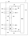
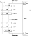
- FIG. 1A is a diagram conceptually showing the overall configuration of the assembled battery of the present invention.
- the assembled battery 1 is obtained by connecting a battery management unit BMU100 and n unit battery boards UBB200 / 1 to 200 / n in a loop through a communication path 300.
- Each unit battery board UBB200 is equipped with a unit battery 500.
- the unit batteries 500 are connected in series and connected to a load or a charger through the power line 400.
- the information transmission of the single loop communication path 300 is shown as the direction from the frontmost unit battery board UBB200 / n at one end to the rearmost unit battery board UBB200 / 1 at the other end.
- the direction is assumed, a communication path in the reverse direction may be used, and the direction is not limited as the present invention.
- FIG. 1B shows a case where the double loop communication paths 301 and 302 are provided.
- the double loop communication path is a redundant configuration assuming a failure, and it may be considered that there are two communication paths 300. Since it is not always necessary for explanation of normal functions, the following explanation assumes a single loop communication path, and a description of the double loop communication path is omitted in principle.
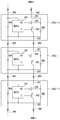
- FIG. 2A shows a specific configuration example of the unit battery board UBB200 and a state of connection between adjacent unit boards.
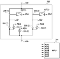
- Each unit battery board UBB200 includes a unit battery UB500, a microprocessor unit MPU201, a transmission signal driver switch 202, an inverter 204, and a resistor 205 as components.
- adjacent unit battery boards UBB200 are connected by a communication connector 600 and a power connector 700.
- the signal line 252 of the front unit battery board UBB200 / i + 1 is connected to the signal line 251 of the unit battery board UBB200 / i through the connector 600, and the reception port R x of the serial communication port of the MPU 201 of the unit battery board UBB200 / i. Are connected to each other through an inverter 204.
- the transmission port T X of serial communication port MPU201 unit cell board UBB200 / i is connected to the base of the signal transmission driver switch 202, by ON ⁇ OFF the driver switch 202, a digital signal a signal line 252
- the digital signal is transmitted to the rear MPU 201 via the connector 600 and the signal line 251 of the rear unit battery board UBB200 / i-1.
- the collector of the driver switch 202 of the unit battery board UBB200 / i is connected to the ground of the rear unit battery board UBB200 / i-1 through the resistor 205 of the rear unit battery board UBB200 / i-1. Therefore, when the driver switch is OFF, a voltage twice as high as that of the unit battery is applied between the emitter and the collector.
- the voltage of the unit battery is nominally 3.7 volts, so that the nominal voltage is twice as high as 7.4 volts, but the semiconductor driver switch 202 can sufficiently withstand the voltage. In this way, each time information is transmitted to the adjacent rear unit battery board UBB, the signal level is shifted down by the potential of one unit battery.
- each unit battery board UBB is connected in a loop shape by the signal lines 251 and 252, the MPU 201, the driver switch 202 and the inverter 204, and constitutes a loop communication path 300.
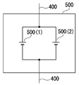
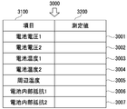
- FIG. 2C illustrates a measurement method of measurement items necessary for calculating the SOC, taking the unit battery of FIG. 2B as an example.
- the unit battery 500 of FIG. 2B has two battery cells 500 (1) and 500 (2). Voltage measurement, temperature measurement, and internal resistance measurement are measured for each cell, and the ambient temperature is a common item. As measured.
- the voltage of the battery cell 500 (1) is digitally measured as the potential of the cell by connecting the positive side of the cell to the analog / digital converter terminal AD 1 of the MPU 201, and the table 3000 ( It is stored in the column 3001 in FIG. 5B).
- the temperature of the battery cell 500 (1) is connected to the AD3 terminal of the MPU 201 by connecting the thermistor 203 (1) attached to the cell, the thermistor potential is measured as a digital value, and further converted into digital as the temperature. It is stored in the column 3003 of the table 3000 (FIG. 5B) on the storage device RAM2012.
- the current sensor 206 (1) is connected to the AD6 terminal of the MPU 201 through the amplifier 207 (1), measured as a digital value, further converted into a digital value as an internal resistance value, and stored in the column 3006 of the table 3000 (FIG. 5B). Is done.
- the voltage, temperature, and internal resistance of the battery cell 500 (2) are measured and stored in columns 3002, 3004, and 3007 of the table 3000 (FIG. 5B). Since the ambient temperature is common to the two battery cells, it is connected to the AD5 terminal of the MPU 201 by the thermistor 203 (p) installed in the air bra in the empty space near the battery cell of the unit battery board 200 and measured as a digital value. Further, it is digitally converted as the ambient temperature and stored in the column 3005 of the table 3000 (FIG. 5B).
- FIG. 3 shows an overall configuration when the unit battery board shown in FIG. 2A is used.
- the unit battery board UBB200 and the battery management unit BMU100 can be disconnected in a direct current manner by transformer coupling, optical coupling, etc., but in a system in which 192 unit cells 500 are connected in series and the total voltage exceeds 700 volts, the unit battery , And the distance between the battery management unit BMU100 and the unit battery board UBB200 group is inevitably increased. Therefore, it is necessary to use a balanced transmission line for the transmission between the battery management unit BMU100 and the unit battery board UBB200 group, and to cut the direct current by transformer coupling or the like.
- balanced transmission using a transformer coupling or the like is used for DC voltage insulation between the last unit battery board UBB200 / 1 and the front unit battery board UBB200 / n and the battery management unit BMU100. Connect by road.
- a balanced transmission path 310 is configured by installing U / B conversion circuits 801 and B / U conversion circuits 802 by transformer coupling or the like at both ends of the transmission path therebetween. By doing so, the high voltage accumulated by the series connection of the unit cells and the battery management unit BMU100 are disconnected in a direct current manner, and the problem of withstand voltage is solved.
- the input / output signal lines of the unit battery board UBB200 are directly connected by a single line as shown in FIG. 2A, and constitute the unbalanced transmission path 300 of FIG.
- FIG. 4 illustrates how the signal from the battery management unit BMU 100 is transmitted to the unit battery board UBB 200 and returns to the battery management unit BMU 100 again in the configuration of FIGS. 2A and 3. *
- the battery management unit BMU 100 converts digital information to be transmitted into a balanced signal by the UB converter 801 and transmits it. This is received by the BU converter 802 placed in front of the front unit battery board UBB200 / n, and the received signal is converted into an unbalanced signal. This signal is sent to all the unit battery boards UBB200 / 1 to 200 / n. Is superimposed on the total voltage.
- Transmitting data from the MPU 201 / n is output from the transmission port T X, the transmission driver switch, ⁇ (n-1) ⁇ E r +0/5 ⁇ as volt signal, the MPU 201 / n of the unit battery board succeeding It is input to the receive port R X -1.
- Information is sequentially transmitted to the subsequent unit battery board in this way, and finally reaches the unit battery board 200/1 as a (0 ⁇ E r +0/5) volt signal, and the MPU 200/1 transmission port is output from the T X, the UB converter 801, are converted into balanced transmission signal is transmitted to the BU conversion circuit 802 of the battery management unit BMU100.
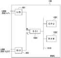
- FIG. 5A is a logical block diagram of hardware of the microprocessor unit MPU201.
- the MPU 201 includes a central processing unit CPU 2011, a primary storage device RAM 2012, a serial communication interface SCI 2013, a plurality of analog / digital converters ADC 2014, a data output DATA 2015, and a bus 2010 as components.
- FIG. 5D shows a configuration of a transmission / reception buffer SRB used for message reception and message transmission.
- Digital data from the unit battery board UBB200 / i + 1 of the previous position takes the receiving port R X, is performed characters assembled in the serial communication interface SCI2013, is stored as a received message in the sending and receiving buffer SRB on the primary storage RAM2012.
- the transmission / reception buffer SRB needs to transfer the received message as it is to the subsequent unit battery board UBB / i-1 while receiving the message from the previous unit battery board UBB200 / i + 1. It consists of a buffer. As for the buffer capacity, since transfer of the received message is performed with a delay of at most 2 bytes, 2 bytes to 3 bytes are sufficient. However, since the transmission message has a maximum structure of 22 bytes (details will be described later), The capacity of the transmission / reception buffer is 32 bytes (a power of 2).
- FIG. 5D shows three registers, that is, a reception byte position counter RBC, a transmission byte position counter SBC, and a required transmission byte number counter SBN that are necessary for the write / read control of the transmission / reception buffer SRB. All three register lengths are 1 byte. The operation will be described later.
- the central processing unit CPU 2011 can instruct signals “high” and “low” to the outside through the ports DO 0 to 1 using the data port DATA 2015. Using this port DO0, ON / OFF of a discharge circuit (not shown) is controlled. Details will be described later.
- FIG. 6A shows a logical block configuration of hardware of the battery management unit BMU100.
- the BMU 100 includes a central processing unit 1001, a primary storage device RAM 1002, a serial communication interface SCI 1003, a U / B converter 801, a B / U converter 802, and a bus 1010 as components.
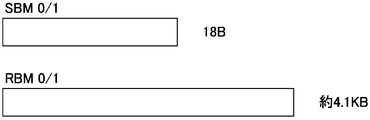
- FIG. 6B shows a transmission buffer and a reception buffer on the primary storage device RAM 1002.
- the transmission message prepared in the transmission buffer SBM0 / 1 on the primary storage RAM 1002 is sent as a balanced transmission signal from the U / B converter 801 via the serial communication interface SCI1003 according to an instruction from the central processing unit CPU1001. It is sent to the unit battery board UBB200 / n. Further, the balanced transmission signal from the last unit battery board UBB200 / 1 is converted into an unbalanced signal by the B / U converter 802, and character assembly is performed by the serial communication interface SCI1003, and reception on the primary storage RAM1002 is performed. It is stored in the buffer RBM0 / 1.
- the capacity 18B and the reception buffer RBM0 / 1 each receive a response of 21 bytes from all unit battery boards at one time.
- 21 bytes X192 4032 bytes are necessary, and the capacity of about 4.1 KB including the transmission command is a two-sided buffer.
- FIG. 7 and 8 show a message format that flows on the loop communication path 300
- FIG. 7 shows a message format transmitted from the BMU 100 to each UBB 200
- FIG. 8 shows a message format sent from each UBB 200 to the BMU 100. Indicates.
- TK that is, a token is described at the tail of all command frames and response frames. This is a general concept, and the command frame and response frames themselves include “ TK "itself is not included. The frame is up to “END”.
- FIG. 9 shows network control signals (generic name CNT) used in a communication protocol for communication using the loop communication path 300
- FIG. 10 shows commands (generic name CMD)
- FIG. 12 shows data (generic name DAT)
- a table 5000 in FIG. 13 shows details of the status.
- FIG. 14 shows the principle of message reception and message transmission of each unit battery board UBB200.
- the reception message ((1) in FIG. 14) of the front unit battery board UBB200 / n includes a command frame from the BMU 200.
- the UBB 200 / n adds its own response frame to the UBB 200 / n, creates a transmission message ((2) in FIG. 14), and sends it to the subsequent unit battery board UBB 200 / n-1.
- the rear unit battery board UBB / n-1 receives this, adds its own response frame to it, creates a transmission message ((3) in FIG. 14), and further adds the rear unit battery board UBB200 / Send to n-2.
- the response frames from all the unit battery boards 200 are returned to the battery management unit BMU 100 while sequentially repeating such operations.
- the battery management unit 200 requests only a response from the specific unit battery board 200 / i, all the UBBs 200 / j (j ⁇ i) other than the UBB 200 / i do not return a response frame, so the UBB 200 Only the response frame from / i is returned.
- TK is called a token and means grant of a transmission right. That is, only the node holding “TK” (in this example, the node holding “TK” among the MBU 100 and UBB 200/1 to 200 / n) is allowed to transmit data. Therefore, the BMU 100 adds “TK” to the end of the command frame and sends it, and grants the transmission right to the front-most unit battery board UBB200 / n ((1) in FIG. 14).
- the UBB 200 / n receiving this command adds its own response frame to the back of the command frame, adds “TK” after the command frame, and sends a message to the rear unit battery board UBB 200 / n ⁇ 1. Is transmitted at the same time as (2) in FIG.
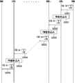
- FIG. 15 is a sequence diagram for obtaining a MAC address report from all unit batteries 200.
- the battery management unit BMU 100 reports the MAC address of each unit battery board UBB 200 to the subordinate unit battery boards UBB 200 for collecting the IDs in the C1 format command frame shown in FIG.
- the message + TK is sent out to the foremost unit battery board UBB200 / n (referred to as UBB n , hereinafter the same) (S1001).
- UBB n Upon receiving this CID command message, UBB n analyzes the message, recognizes that it is a CID command addressed to all UBBs, sets its own MAC address in the ID field of the R1 format response frame shown in FIG. An n response is created, inserted between the END mark of the CID command and the subsequent TK mark, and sent to the subsequent unit battery board UBB n-1 in the order of the CID command, the ID n response, and TK (S1002). .
- UBB n-1 which has received this, using its own MAC address in the same way, to create a ID n-1 response, CID command, ID n response, ID n-1 response, further after position in the order of TK It is sent to UBB n-2 (S1003).
- the last UBB 1 receives the CID command, ID n response, ID n-1 response,... ID 2 response, TK from the previous UBB 2 (S1004), and sends it to the BMU.
- the ID 1 response is inserted before TK and sent (S1005).
- two BMUs are written on the left and right sides of the drawing. This is because the loop communication path is displayed in an expanded view, and is actually one BMU.
- step S ⁇ b> 1005 the BMU analyzes the received MAC addresses as the IDs of all UBBs and confirms that the unit battery board manufactured by the manufacturer is permitted to be incorporated in the assembled battery 1.
- a network address NAD used in the assembled battery 1 is created corresponding to each MAC address, and notified to each UBB by the SNAD command. This is shown in the lower part of FIG.
- NAD i is assigned to each ID i, and a total of n NAD grant messages are sent (S1011 to S1013).
- Each UBB i takes in the NAD i addressed to itself by ID i corresponding to its own MAC address, and communication between the BMU 100 and the UBB 200 / i is performed using this NAD i thereafter.
- FIG. 16 shows a sequence when the BMU 100 requests the UBB 200 to send data such as measured voltage.
- Request for measurement data in the C1 form command frame, and sets the NAD i of the target UBB i in DA, sends the RV command (S2001).
- UBB j whose NAD i indicated in DA does not coincide with its own NAD j even if the RV command is received, does not do anything and transfers the command as it is to UBB j-1 at the succeeding position (S2002).
- the procedure for reporting the measured temperature and measured internal resistance is essentially the same as that for reporting the measured voltage. However, if the report data was extracted in response to the command and a response message was created, the processing efficiency would be reduced. Regardless of the message, the position on the response frame of the measurement data is fixed (see Fig. 8), and the voltage, temperature, and internal resistance are arranged in order from the most important and frequently reported. Prepare in the form of an R4 response frame so that all data can be returned. This is called a preparation response frame ARF (Arranged Response Frame), which is prepared on the primary storage device RAM 2012.
- ARF Arranged Response Frame
- RV command only the upper voltage is returned (R2 format response frame), for the RT command, both voltage and temperature are returned (R3 format response frame), and for the RR command, By returning all of the voltage, temperature, and internal resistance (R4 format response frame), the processing for each command is minimized and the load on the central processing unit is reduced.
- status information is included in all response frames from R2 to R4, and this is also prepared as an R4 command together with other measurement data each time information is collected. Reply with response frame.
- each UBB takes the designated unit battery specified voltage value in the same manner as a reference voltage value for equalization, stores it in the column 4001 of the table 4000 on the primary storage device 2012, and stores the EQL command frame in the rear position. Therefore, all UBBs can take the designated unit battery specified voltage value as a reference voltage value for equalization.
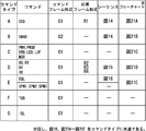
- FIGS. 19A to 22 are flowcharts showing various operations of the unit battery board UBB200.
- the commands received by the unit battery board UBB200 from the battery management unit BMU100 are as shown in FIG. 10, and these are as shown in FIG. 18 when classified by the type of processing in the unit battery board UBB200.
- the command types A and D create a response frame and return it to the battery management unit BMU 100, and the details will be described with reference to flowcharts (FIGS. 20A to E and FIGS. 21A to 21E).
- the type E EQL command does not create a response frame, but is a process specific to the assembled battery, and will be described in detail with reference to a flowchart (FIG. 22). All other types are closed to processing in the unit battery board and are simple operations, and thus detailed description thereof is omitted here.
- the serial communication interface SCI 2013 executes character assembly of received data, completes the assembly of 1 byte, and interrupts the central processing unit CPU 2011 every time writing and storing of the byte is completed in the transmission / reception buffer SBR. Therefore, this starts (S5000).
- the received byte data is written in the transmission / reception buffer SRB on the primary storage device RAM 2012 using the lower 5 bits of the reception byte position counter RBC (FIG. 5D) as an index.
- the CPU 2011 detects the interrupt, starts the program (S5000), refers to the lower 5 bits “b r ” of the reception byte counter RBC, and corresponds to the byte positions b r ⁇ 1 and b r on the transmission / reception buffer.
- Two bytes are read (S5001), and the contents of the TOP register (not shown) are referred to, and it is checked whether there is a reception history of the network control signal “TOP” in the past.
- reception history S5002, NO
- the serial communication interface 2013 is instructed to transfer the contents of the transmission / reception buffer, that is, “TOP” to the subsequent unit battery board UBB 200 as it is (S5022), and the reception byte position counter RBC is prepared for the storage of the next reception byte. Is updated by "1" (S5023), and the process ends (S5030).
- the serial communication interface SCI 2013 that receives the transmission instruction generates an interrupt to the central processing unit CPU 2011 when the one-byte transmission processing is completed.
- FIG. 19C shows an operation flow of the central processing unit CPU 2011 after detecting the interrupt.
- the transmission byte position counter is incremented by “1” (S4102), the transmission byte count counter SBN is decremented by “1” (S4103), and a transmission instruction is sent to the SCI. (S4104) and the process ends (S4130).
- FIG. 19D shows an operation flow of the serial communication interface SCI 2013 that has received a transmission instruction.
- the transmission instruction is started (S4200) and the value of the required transmission byte counter SBN is “0” (S4201, YES), it is determined that there is no byte to be transmitted, and the rear unit battery board UBB / i For -1, an IDLE signal is transmitted (S4202), and the process ends (S4230).
- S5101 is YES, it indicates that the command is for all unit batteries UBB, so CMD is set to 1 for command waiting registration (S5103).
- the reception byte position counter is incremented by “1” (S5023), and the process is terminated (S5030).
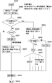
- FIG. 21A shows a flowchart for process A
- FIG. 21B shows process B
- FIG. 21C shows process C
- FIG. 21D shows process D
- FIG. The processes F and G are omitted.
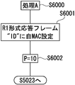
- FIG. 21A is a flow when a CID command is received.
- the local MAC address that is, a 6-byte, 48-bit address is set in the ID to create a response frame in the R1 format (S6001).
- the required transmission byte count p is set to a response frame length of 10 bytes in the R1 format (S6002), the reception byte position counter RBC is incremented by "1" (S5023), and the process ends (S5030).
- FIG. 21B is a flow when the SNAD command is received.
- the process starts with reception of a SNAD command (S6100), and it is determined whether or not SNAD is received and registered (S6101). Since S6101, YES indicates that it has not been received in the past, reception registration is performed (S6102), the reception byte position counter RBC is incremented by "1" (S5023), and the process ends (S5030). Since NO is illegal in S6101, TOP is reset (S6103), the reception byte position counter RBC is incremented by "1" (S5023), and the process ends (S5030).
- FIG. 21C shows a flow upon receipt of PWH, PWSD, ERB, LED, LOF, and MSR commands. Since any command instructs the operation in the unit battery board UBB, the operation of the loop communication path is not affected after the command is received, and thus detailed description thereof is omitted.
- FIG. 21D shows a flow when RS, RV, RT, and RR commands are received.
- R2 format response frames are created for RS and RV commands
- R3 and R4 format response frames are created for RT and RR commands, respectively (S6301).
- FIG. 21E shows a flow when the commands EQL, SPM1, SPM2, and SPM3 are received.
- the command is started upon receipt (S6400).
- the PM value (TPM) primarily stored in S5201 is entered in the corresponding column of the table 4000 (S6401). That is, in the case of the EQL command, it is described in the column 4001, and in the case of the SPM1 command, it is described in the column 4002.
- the reception byte position counter RBC is incremented by “1” (S5023), and the processing is terminated (S5030).
- reception byte position counter RBC is incremented by “1” (S5023), and the process ends (S5030).
- SNAD command if the received after the third word (S5512, YES), 3 words (6 bytes, 48 bits) of byte positions b r -5 transceiver Buffers from, b r determines whether it is its own MAC address (S5514 ). If it matches the own MAC address (S5514, YES), the content of the TPM stored in S5201 is set as its own DA (S5515) and used as its own unit battery board address in communication with the post-battery battery management unit BMP100. .
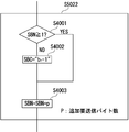
- FIG. 22 shows a normalization in unit battery board UBB200 when receiving a normal voltage measurement and an EQL command and describing a unit battery designated voltage value of PM value as a reference voltage value for equalization in column 4001 of table 4000 It is a flowchart which shows operation
- the voltage value of the unit battery UB500 held in the column 3001 or 3002 of the table 3000 is compared with the captured PM value, that is, the unit battery designated voltage value (S5804). If the holding voltage is higher (S5804, YES), the central processing unit CPU2011 sets the data port DO0 to “high” to turn on the discharge circuit (not shown) (S5805), and ends (S5820). Thereby, the unit battery board UBB starts the equalization operation.
- temperature measurement other than battery voltage measurement internal resistance measurement also by timer interrupt, For example, temperature measurement is performed with a 1S interrupt, and internal resistance measurement is performed with a 10S interrupt. Since the execution procedure is the same as in the case of battery voltage measurement, detailed description is omitted.
- FIG. 23A shows a remote power ON / OFF circuit of the battery pack of the present invention. Since the voltage of the unit battery of the assembled battery has a voltage unique to the unit battery, a DC-DC converter is used to obtain a voltage convenient for stably operating the electronic circuit of the unit battery board UBB200.
- the unit cell board UBB n signal lines 251 "high" to change held by the DDC204 E terminal is "high” next, become DDC204 operating state, a voltage is supplied to the input VI Therefore, the DCC 204 generates a voltage at the output VO and supplies the Vcc of the MPU 201.
- the MPU 201 receiving the Vcc supply is in an operating state, and the data terminal DO1 is set to “high” for self-holding of the power source, and the DDC 204 is self-held.
- the MPU 201 sets the transmission port T x to “high” and sets the subsequent UBB n ⁇ 1 to the operating state. This operation is sequentially transmitted, and finally, all UBBs up to UBB 1 enter an operation state, and the assembled battery 1 enters an operation state.
- the battery management unit (this unit needs to be constantly supplied) is first switched to a low bit.
- a signal of a rate (for example, 1 kbps) is sent to the front unit battery board UBB n .
- This low bit rate data signal undergoes U / B and B / U conversion and is transmitted to the signal line 251 of the frontmost UBB n .
- the signal line 251 is held at “high” for a short time (several hundred ⁇ s). This time is sufficient for the DDC 204 to wake up and for the MPU 201 to issue a self-holding signal.
- Such MPU201 of UBB n in the can and into the operating state transmits a port T X and "high", and shifts the UBB n-1 of the succeeding operational. This operation is sequentially repeated, and finally the last UBB 1 enters the operation state, and the assembled battery 1 can be brought into the operation state as a whole.
- FIG. 23B shows a method of waking up the DC-DC converter 204 with high-speed data information. Even when the DC-DC converter 204 is turned ON and the MPU 201 is further operated to enter a self-holding state, a “high” state sufficient for the signal line 251 cannot be expected, the circuit of FIG. For example, the DC-DC converter 204 is sufficiently operated even with a small amount of power obtained by direct-current reproduction of the data signal waveforms of a plurality of continuous power holding commands sent from the BMU 100, and the self-holding circuit of the MPU 201 is turned on. Is possible.
- the battery management unit BMU 100 continuously sends a plurality of command frames having a power holding command PWH to the frontmost UBB n , and receives the command frame having the command PWH from the last UBB 1 , thereby operating all unit batteries. It can enter a state and can confirm completion of starting of the assembled battery 1.
- the battery management unit BMU 100 sends the power holding release command PHSD to the forefront UBB n as described above, and then sequentially stops all the unit batteries 200 by stopping data transmission. It can be turned off. Even if the power holding release command PHSD is not displayed, if there is no data input for a long time and the signal line 251 continues “low”, the MPU 201 performs “low” self-holding by timer monitoring. It is effective to set the DDC 204 to be OFF.
- the unit battery board UBB200 only responds to commands from the battery management unit BMU100, but actively operates when the loop communication path 300 is disconnected due to a failure.
- the BMU 100 always sends out the token TK within a certain time. This is realized by adding a TK to a command for issuing various commands to the unit battery board 200. If no command is given, an idle command IDL is sent, and a TK is added after that.
- each unit battery board UBB200 cannot receive the token TK within a certain time, it is determined that the loop communication path is abnormal, and the unit battery board UBB200 creates a token loss command TKL and sends it to the subsequent unit battery board UBB200. .
- This TKL command is relayed by each unit battery board UBB200 and finally transmitted to the battery management unit BMU100, and the BMU can request a service from the maintenance department as a communication path failure.
- the NAD i (see FIG. 8) of the TKL command frame (C3 format command frame) received by the BMU 100, it can be detected as a communication path failure immediately before the i-th UBB or an i + 1-th UBB failure.
- the operation can be continued using the communication path 302.
- a TKL command frame is sent from UBB i-1 via the communication path 301, and a TKL command is sent from UBB i + 1 via the communication path 302. Therefore, it can be determined that UBB i is faulty, and if both of the communication paths between the i + 1th and i-th unit battery boards UBB are faulty, a TKL command is sent from UBB i by the communication path 301. Since the TKL command is sent from the UBB i + 1 via the communication path 302, it is possible to determine that the communication path is double fault between UBB i and UBB i + 1, which is effective in repairing the fault.
- the assembled battery 1 has been described in a mode in which the unit cells 500 are connected in series.
- the unit cell 500 (1) and the unit cell 500 (2) are connected in parallel, such n sets of parallel-connected unit cells are connected in series, and UBB (1) and 500 (2) on which each unit cell 500 (1) is mounted are mounted on UBB.
- the number of unit cells connected in parallel is not limited to two.
Abstract
Description
バッテリ管理ユニット間を直流絶縁することは容易であり、バッテリ管理ユニットにおける耐圧制限の問題は解消できる可能性は大きい。したがって、バッテリ管理ユニットと単位電池ボードを接続するにあたって、非特許文献1のように単位電池ボード8個毎にセル情報計測通信制御装置を設置する必要はなくなる。
図1Aは本発明の組電池の全体構成を概念的に示す図である。組電池1は、バッテリ管理ユニットBMU100と、n個の単位電池ボードUBB200/1~200/nとが通信路300でループ状に接続されたものである。また、各単位電池ボードUBB200には、単位電池500が搭載されており、単位電池500は、直列に接続され、電力ライン400を通して負荷または充電器に接続される。
このようにして、各単位電池ボードUBBは、信号線251及び252とMPU201、ドライバスイッチ202及びインバータ204によってループ状に接続され、ループ状通信路300を構成する。
周囲温度は二つの電池セルに共通するので、単位電池ボード200の電池セル近辺の空きスペースに宙ブラに設置されたサーミスタ203(p)によって、MPU201のAD5端子に接続され、ディジタル値として測定され、さらに周辺温度としてディジタル変換され、テーブル3000(図5B)の3005欄に記憶される。
情報は順次このようにして、後位の単位電池ボードに伝達され、最終的には単位電池ボード200/1に(0・Er+0/5)ボルト信号として到達し、MPU200/1の送信ポートTXより出力され、UB変換器801により、平衡伝送信号に変換されて、バッテリ管理ユニットBMU100のBU変換回路802に伝達される。
最前の単位電池ボードUBB200/nの受信メーセージ(図14の(1))には、BMU200からのコマンドフレームが含まれている。UBB200/nは、これに自己の応答フレームを付加して、送信メッセージ(図14の(2))を作成し、後位の単位電池ボードUBB200/n-1に送付する。これを後位の単位電池ボードUBB/n-1が受信し、それに自己の応答フレームを付加して、送信メッセージ(図14の(3))を作成し、さらに後位の単位電池ボードUBB200/n-2に送付する。
そこで、BMU100は、コマンドフレームの後尾に“TK”を付加して送付し、送信権を最前位の単位電池ボードUBB200/nに授与したものである(図14の(1))。
測定データの要求は、C1形式コマンドフレームに於いて、DAに対象UBBiのNADiを設定し、RVコマンドを送付する(S2001)。当該RVコマンドを受信してもDAに示されたNADiが自己のNADjと一致しないUBBjは、特に何もせずに後位のUBBj-1に該コマンドをそのまま転送する(S2002)。
単位電池500の電圧の均等化は全UBB200を対象に行うので、C1形式コマンドフレームのDAをall“0”に設定し、PMに均等化のための単位電池指定電圧値を設定したEQLコマンドを最前位のUBB200/nに向けて送出する(S2021)。
図19Cは、該割り込みを検知した後の中央処理装置CPU2011の動作フローを示す。
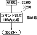
図21Aに処理A、図21Bに処理B、図21Cに処理C、図21Dに処理D、図21Eに処理Eについてのフローチャートを示す。処理F,Gについては省略する。
要送信バイト数pをR1形式の応答フレーム長10バイトに設定(S6002)して、受信バイト位置カウンタRBCを“1”だけ加算して(S5023),終了(S5030)する。
各コマンドの受領で開始(S6300)し、RS及びRVコマンドに対してはR2形式応答フレームを作成、RT及びRRコマンドに対しては、それぞれR3及びR4形式の応答フレームを作成する(S6301)。
次に、受信バイト位置カウンタRBCを“1”だけ加算して(S5023)、終了(S5030)する。
“END”と判定された場合(S5510、YES)、“END”受信を登録(S5511)し、受信バイト位置カウンタRBCを“1”だけ加算して(S5023),終了(S5030)する。
例えば温度測定は、1S割り込みで、内部抵抗測定は、10S割り込みで行う。実行手順は、電池電圧測定の場合と同じであるので、詳細説明は省略する。
組電池1が不動作時には、バッテリ管理ユニット100から予め、PWSDコマンドが全単位電池宛UBB200に送付され、電源自己保持用に使用されるMPU201のデータ出力端子DO1が“low”に設定されている。
BMU100は常に一定の時間内に必ずトークンTKを送出する。単位電池ボード200に各種の指令を出すコマンドにTKを付加することで実現するが、指令することがない場合には、アイドルコマンドIDLを送出し、その後ろにTKを付加する。
100 バッテリ管理ユニットBMU
200/n 単位電池ボードUBB/n
201 マイクロ・プロセッサ・ユニットMPU
202 送信信号用ドライバスイッチ
203 サーミスタ
204 インバータ
205 抵抗
206 電流センサ
207 アンプ
208 DC-DC変換器
251 信号受信線
252 信号送信線
300、301、302、310 通信路
400 電力ライン
500 単位電池
600 信号線用コネクタ
700 電力線用コネクタ
801 U/B変換回路
802 B/U変換回路
1001 中央処理装置CPU
1002 一次記憶装置RAM
1003 シリアル通信インタフェースSCI
1010 バス回路
2010 バス回路
2011 中央処理装置CPU
2012 一次記憶装置RAM
2013 シリアル通信インタフェースSCI
2014 アナログ・ディジタル変換器ADC
2015 データ制御DATA
3000 測定値テーブル
3100 測定項目
3200 測定値
4000 PM値取り込みテーブル
4100 取り込み項目
4200 取り込み値
AD「 」 アナログ・ディジタル変換ポート「 」
ARF 準備応答フレーム
Er 電池公称起電力
p 追加して送信すべきバイト数
RBC 受信バイト位置カウンタ
RBM 受信バッファメモリ
SBC 送信バイト位置カウンタ
SBM 送信バッファメモリ
SBN 要送信バイト数カウンタ
SRB 送受信バッファ
WRF 送信待応答フレーム
Claims (15)
- 複数の単位電池を接続して構成される組電池であって、
各単位電池を搭載した単位電池ボードと該複数の単位電池ボードに共通のバッテリ管理ユニットを構成要素として有し、
個別単位電池ボード毎に
搭載された単位電池の電圧、単位電池の温度、単位電池の周辺温度及び単位電池の内部抵抗のすべて又はその一部の測定及び該測定値を保持する手段と
該保持した測定値を該バッテリ管理ユニットにディジタル信号として送信する手段と
該バッテリ管理ユニットよりディジタル信号として送られて来る単位電池指定電圧値を受信する手段と
を有することを特徴とする組電池。
- 請求項1に記載の組電池であって、
該複数の単位電池ボードと該バッテリ管理ユニットとが1重のループ状通信路又は2重のループ状通信路により接続され、該ループ状通信路を介して該各単位電池ボードと該バッテリ管理ユニット間で、該測定値、該単位電池指定電圧値および関連制御情報の送受を行うこと
を特徴とする組電池。
- 請求項1または請求項2に記載の組電池であって、
個別単位電池ボードに1個の電池セルまたは相互に接続された複数個の電池セルが搭載され、それぞれの電池セル毎に電池電圧、電池温度、電池内部抵抗のすべて又は一部の測定及び該測定値を保持する手段を有することを特徴とする組電池。
- 請求項1から請求項3のいずれかに記載の組電池であって、
各個別単位電池ボートにおいて、
該保持した単位電池電圧の測定値が該受信した単位電池指定電圧値より高い場合に、当該単位電池ボード内の電池セルの放電を開始し、
同等または低い場合に、当該電池セルの放電を停止または停止状態を継続することを特徴する組電池。
- 請求項1から請求項4のいずれかに記載の組電池であって、
各単位電池ボードは、前位より送られてくるフレームの宛先アドレスが全単位電池ボード宛で、かつ該フレームのコマンドが情報要求コマンドの場合に、該フレーム情報のすべてを後位にそのまま転送するとともに、トークンを検出後、該フレームの最後尾と該検出したトークンとの間に当該要求された情報を挿入して後位に送出することを特徴とする組電池。
- 請求項1から請求項5のいずれかに記載の組電池であって、
個別単位電池ボード毎に
搭載された単位電池の電圧、単位電池の温度、単位電池の内部抵抗及び周辺温度のすべて又は一部の測定及び該測定値を保持する手段と、
該保持した測定値を該バッテリ管理ユニットへ送信をする手段と、
該バッテリ管理ユニットからの単位電池の指定電圧値を受信する手段と、
該保持した測定値と該受信した単位電池指定電圧値とを比較し、比較結果に従い充放電制御をする手段とを有し、
それらの手段を1つのマイコンで実行制御する組電池。
- 請求項1から請求項6のいずれかに記載の組電池であって、
該バッテリ管理ユニットが全単位電池ボードより単位電池電圧情報、単位電池温度情報、単位電池内部抵抗情報、単位電池周辺温度情報およびステータス情報のすべて又は一部を収集するために、ループ状通信路で接続された単位電池ボード群の一端の単位電池ボードに向けて全単位電池ボード宛または特定の単位電池ボード宛に情報要求のフレームを送信し、他端の単位電池ボードより、全単位電池ボードまたは該特定の単位電池ボードの当該情報を受信することを特徴とする組電池。
- 請求項1から請求項7のいずれかに記載の組電池であって、
一のループ状通信路を構成する隣接単位電池ボード間の接続を単線で構成することを特徴とする組電池。
- 請求項8に記載の組電池であって、
各単位電池ボードが前位より受信する情報の信号レベルに対して、後位に送信する情報の信号レベルを単位電池の電位差分だけレベルシフトして送付することを特徴とする組電池。
- 請求項1から請求項9のいずれかに記載の組電池であって、
該バッテリ管理ユニットが複数の単位電池ボードより送られてくる各単位電池の電圧情報、温度情報、内部抵抗情報又は周囲温度情報を分析する手段と、
該各単位電池の維持すべき電圧値を算出する手段と、
該電圧値を単位電池指定電圧値として全単位電池ボード宛または特定単位電池ボード宛に送出する手段と
を有することを特徴とする組電池。
- 請求項8または請求項9に記載の組電池あって、
各単位電池ボードに搭載されるマイクロプロセッサは、
電源供給を受けた直後にデータ端子を“high”に設定する手段と
バッテリ管理ユニットより自己保持回路を解除せよとのコマンドを受信すると該データ端子を“low”に設定する手段とを有し、
各単位電池ボードに搭載されるDC-DCコンバータは、そのイネーブル端子に前位の隣接単位電池ボードとを結ぶ信号線にバッテリ管理ユニットより送られてくるデータ信号波形の“high”状態の継続内に、動作状態になり、出力電圧を生じることによって、該マイクロプロセッサに電源供給を行い、該マイクロプロセッサは直後に前述のデータ端子を“high”に設定する手段により、該データ端子は“high”に設定され、該DC-DCコンバータの自己保持回路を形成し、
また、該マイクロプロセッサは、バッテリ管理ユニットから、自己保持回路を解除せよとのコマンドを受信すると前述の該データ端子を“low”に設定する手段により、該データ端子を“low”に設定し、該DC-DCコンバータの自己保持回路を解除し、
その状態で該DC-DCコンバータは、そのイネーブル端子に前位の隣接単位ボードとを結ぶ信号線にバッテリ管理ユニットより送られてくるデータ信号波形が“low”の状態に保持された時に、その動作を停止し、出力電圧を失い、該マイクロプロセッサへの電源供給が停止される
ことを特徴とする組電池。
- 請求項11に記載の組電池であって、
前位の隣接単位電池ボードとを結ぶ信号線にバッテリ管理ユニットより送られてくるデータ信号波形の“high”状態の継続によらず、該データ信号波形を直流再生して得られる信号を該イネーブル端子に受けてDC-DCコンバータが動作状態になることを特徴とする組電池。
- コンピュータに請求項6に記載の各種手段を実行させるためのソフトウエアプログラム。
- コンピュータに請求項10に記載の各種手段を実行させるためのソフトウエアプログラム。
- コンピュータに請求項11に記載の各種手段を実行されるためのソフトウエアプログラム。
Priority Applications (2)
| Application Number | Priority Date | Filing Date | Title |
|---|---|---|---|
| CN2011800118012A CN102918739A (zh) | 2010-03-01 | 2011-02-15 | 电池组 |
| US13/581,522 US20130066572A1 (en) | 2010-03-01 | 2011-02-15 | Assembled battery |
Applications Claiming Priority (2)
| Application Number | Priority Date | Filing Date | Title |
|---|---|---|---|
| JP2010-044769 | 2010-03-01 | ||
| JP2010044769A JP5467597B2 (ja) | 2010-03-01 | 2010-03-01 | 組電池 |
Publications (1)
| Publication Number | Publication Date |
|---|---|
| WO2011108201A1 true WO2011108201A1 (ja) | 2011-09-09 |
Family
ID=44541872
Family Applications (1)
| Application Number | Title | Priority Date | Filing Date |
|---|---|---|---|
| PCT/JP2011/000826 WO2011108201A1 (ja) | 2010-03-01 | 2011-02-15 | 組電池 |
Country Status (5)
| Country | Link |
|---|---|
| US (1) | US20130066572A1 (ja) |
| JP (1) | JP5467597B2 (ja) |
| CN (1) | CN102918739A (ja) |
| TW (1) | TWI566497B (ja) |
| WO (1) | WO2011108201A1 (ja) |
Cited By (1)
| Publication number | Priority date | Publication date | Assignee | Title |
|---|---|---|---|---|
| WO2014038081A1 (ja) * | 2012-09-10 | 2014-03-13 | ルネサスエレクトロニクス株式会社 | 半導体装置及び電池電圧監視装置 |
Families Citing this family (20)
| Publication number | Priority date | Publication date | Assignee | Title |
|---|---|---|---|---|
| US9184605B2 (en) * | 2011-03-28 | 2015-11-10 | Changs Ascending Enterprise Co., Ltd. | High voltage battery system for vehicle applications |
| WO2012144674A1 (ko) * | 2011-04-22 | 2012-10-26 | Sk 이노베이션 주식회사 | 착탈 가능한 배터리 모듈, 이를 이용한 배터리 스트링을 위한 전하 균일 방법 및 장치 |
| KR101540086B1 (ko) * | 2012-01-19 | 2015-07-28 | 주식회사 엘지화학 | 멀티 bms 기동 시스템 및 방법 |
| JP5910129B2 (ja) * | 2012-02-06 | 2016-04-27 | ソニー株式会社 | 電力貯蔵装置、電力システムおよび電動車両 |
| JP6005445B2 (ja) * | 2012-08-29 | 2016-10-12 | 日立オートモティブシステムズ株式会社 | 電池システム監視装置 |
| KR101539693B1 (ko) * | 2012-10-04 | 2015-07-27 | 주식회사 엘지화학 | 멀티 bms 기동 장치 |
| JPWO2014076839A1 (ja) * | 2012-11-19 | 2017-01-05 | 日立化成株式会社 | 蓄電池電圧平準化装置および蓄電池状態監視システム |
| CN103944197A (zh) * | 2013-01-17 | 2014-07-23 | 能元科技股份有限公司 | 电池管理光纤传输系统及其电池管理方法 |
| US9041454B2 (en) | 2013-03-15 | 2015-05-26 | Atieva, Inc. | Bias circuit for a switched capacitor level shifter |
| US10084214B2 (en) * | 2013-03-15 | 2018-09-25 | Atieva, Inc. | Automatic switchover from cell voltage to interconnect voltage monitoring |
| WO2014155412A1 (ja) * | 2013-03-25 | 2014-10-02 | 三洋電機株式会社 | 蓄電池管理システム |
| KR101768251B1 (ko) | 2013-04-05 | 2017-08-30 | 삼성에스디아이 주식회사 | 배터리 모듈의 정상 연결 상태 확인을 제공하는 배터리 팩 |
| DE102014200340A1 (de) | 2014-01-10 | 2015-07-16 | Robert Bosch Gmbh | Verfahren zur Datenübertragung von Messdaten in einer Batterie, die mehrere Batteriezellen aufweist |
| CN106461731B (zh) * | 2014-04-02 | 2019-12-10 | 特斯拉公司 | 能量存储系统中通信和数据传输的功能的冗余 |
| FR3023006B1 (fr) * | 2014-06-26 | 2016-06-24 | Renault Sa | Systeme de batteries d'accumulateurs a mesure de tension fiabilisee |
| TWI505531B (zh) * | 2014-08-05 | 2015-10-21 | Quanta Comp Inc | 備用電池 |
| US10741888B2 (en) | 2017-06-30 | 2020-08-11 | Tesla, Inc. | Multi-channel and bi-directional battery management system |
| KR102202613B1 (ko) | 2017-09-27 | 2021-01-12 | 주식회사 엘지화학 | 배터리 모듈 균등화 장치, 이를 포함하는 배터리 팩 및 자동차 |
| EP3767778B1 (en) * | 2018-03-15 | 2023-10-04 | Yamaha Hatsudoki Kabushiki Kaisha | Battery control system for nickel-metal hydride battery |
| CN209055581U (zh) * | 2018-09-17 | 2019-07-02 | 宁德时代新能源科技股份有限公司 | 采样组件及电池包 |
Citations (6)
| Publication number | Priority date | Publication date | Assignee | Title |
|---|---|---|---|---|
| GB2312571A (en) * | 1996-04-24 | 1997-10-29 | Fuji Heavy Ind Ltd | Charging series connected batteries |
| WO2002001695A1 (fr) * | 2000-06-27 | 2002-01-03 | Fujitsu Ten Limited | Systeme de chargement/de dechargement de pile |
| JP2007059088A (ja) * | 2005-08-22 | 2007-03-08 | Nissan Motor Co Ltd | 組電池 |
| EP1933443A2 (en) * | 2006-12-13 | 2008-06-18 | AMI Semiconductor Belgium BVBA | Power cell monitoring |
| JP2009044802A (ja) * | 2007-08-06 | 2009-02-26 | Pues Corp | 電圧均等化制御装置 |
| JP2009106018A (ja) * | 2007-10-22 | 2009-05-14 | Pues Corp | 充電装置及び充電方法 |
Family Cites Families (9)
| Publication number | Priority date | Publication date | Assignee | Title |
|---|---|---|---|---|
| JP3909609B2 (ja) * | 1996-02-09 | 2007-04-25 | 本田技研工業株式会社 | 車両制御用通信網およびその診断方法 |
| US5764027A (en) * | 1996-06-21 | 1998-06-09 | Ford Global Technologies, Inc. | Method and apparatus for battery charge balancing |
| DE69940909D1 (de) * | 1998-07-21 | 2009-07-02 | Metrixx Ltd | Signalisierungssystem |
| DK2024519T3 (da) * | 2006-05-15 | 2021-12-13 | A123 Systems Llc | Multikonfigurerbart, skalerbart, redundant batterimodul med multipel fejltolerance |
| WO2008095315A1 (en) * | 2007-02-09 | 2008-08-14 | Advanced Lithium Power Inc. | Battery management system |
| US7777451B2 (en) * | 2007-04-17 | 2010-08-17 | Chun-Chieh Chang | Rechargeable battery assembly and power system using same |
| TWI351779B (en) * | 2007-12-03 | 2011-11-01 | Advance Smart Ind Ltd | Apparatus and method for correcting residual capac |
| US8089248B2 (en) * | 2009-04-09 | 2012-01-03 | Ford Global Technologies, Llc | Battery monitoring and control system and method of use including redundant secondary communication interface |
| JP5333126B2 (ja) * | 2009-09-29 | 2013-11-06 | 株式会社デンソー | 組電池制御装置 |
-
2010
- 2010-03-01 JP JP2010044769A patent/JP5467597B2/ja active Active
-
2011
- 2011-02-15 WO PCT/JP2011/000826 patent/WO2011108201A1/ja active Application Filing
- 2011-02-15 CN CN2011800118012A patent/CN102918739A/zh active Pending
- 2011-02-15 US US13/581,522 patent/US20130066572A1/en not_active Abandoned
- 2011-02-23 TW TW100105909A patent/TWI566497B/zh not_active IP Right Cessation
Patent Citations (6)
| Publication number | Priority date | Publication date | Assignee | Title |
|---|---|---|---|---|
| GB2312571A (en) * | 1996-04-24 | 1997-10-29 | Fuji Heavy Ind Ltd | Charging series connected batteries |
| WO2002001695A1 (fr) * | 2000-06-27 | 2002-01-03 | Fujitsu Ten Limited | Systeme de chargement/de dechargement de pile |
| JP2007059088A (ja) * | 2005-08-22 | 2007-03-08 | Nissan Motor Co Ltd | 組電池 |
| EP1933443A2 (en) * | 2006-12-13 | 2008-06-18 | AMI Semiconductor Belgium BVBA | Power cell monitoring |
| JP2009044802A (ja) * | 2007-08-06 | 2009-02-26 | Pues Corp | 電圧均等化制御装置 |
| JP2009106018A (ja) * | 2007-10-22 | 2009-05-14 | Pues Corp | 充電装置及び充電方法 |
Cited By (4)
| Publication number | Priority date | Publication date | Assignee | Title |
|---|---|---|---|---|
| WO2014038081A1 (ja) * | 2012-09-10 | 2014-03-13 | ルネサスエレクトロニクス株式会社 | 半導体装置及び電池電圧監視装置 |
| CN104603627A (zh) * | 2012-09-10 | 2015-05-06 | 瑞萨电子株式会社 | 半导体装置和电池电压监视装置 |
| US9564765B2 (en) | 2012-09-10 | 2017-02-07 | Renesas Electronics Corporation | Semiconductor device and battery voltage monitoring device |
| CN104603627B (zh) * | 2012-09-10 | 2017-11-03 | 瑞萨电子株式会社 | 半导体装置和电池电压监视装置 |
Also Published As
| Publication number | Publication date |
|---|---|
| JP2011182558A (ja) | 2011-09-15 |
| US20130066572A1 (en) | 2013-03-14 |
| TW201206011A (en) | 2012-02-01 |
| TWI566497B (zh) | 2017-01-11 |
| CN102918739A (zh) | 2013-02-06 |
| JP5467597B2 (ja) | 2014-04-09 |
Similar Documents
| Publication | Publication Date | Title |
|---|---|---|
| JP5467597B2 (ja) | 組電池 | |
| CN110178261B (zh) | 主电池管理单元和包括主电池管理单元的电池组 | |
| KR101107999B1 (ko) | 전압 센서와 전하 균일 장치가 결합된 배터리 운용 시스템 | |
| CN101878558B (zh) | 电池管理系统以及充电器 | |
| JP3922655B2 (ja) | 電源装置の制御システムおよび電源装置の制御方法 | |
| US20170222275A1 (en) | Automatic addressing of battery nodes in a battery system | |
| JP4987581B2 (ja) | 電池制御装置 | |
| JP5250230B2 (ja) | 車両用電源システムおよび電池セル制御用集積回路 | |
| US9035611B2 (en) | Battery system for vehicle | |
| CN103563210A (zh) | 包括模块化bms连接结构的电力储存系统及其控制方法 | |
| US9653928B2 (en) | Battery pack including sensing board and power storage system employing the same | |
| KR20190011568A (ko) | 배터리 관리 유닛 및 이를 포함하는 배터리팩 | |
| WO2010038347A1 (ja) | 電池均等化回路、及び電池電源装置 | |
| CN105637728A (zh) | 蓄电池装置和蓄电池系统 | |
| CN102165626A (zh) | 多串联/多并联电池组 | |
| JP7127248B2 (ja) | バッテリー管理システム、バッテリー管理方法、バッテリーパック及び電気車両 | |
| CN109278589B (zh) | 基于pic单片机的双向主动均衡电动汽车电池监控系统及控制方法 | |
| CN205564907U (zh) | 一种电池模组、电池包及车辆 | |
| KR101877564B1 (ko) | 배터리 팩 | |
| JP2010025824A (ja) | 組電池組電池監視装置 | |
| EP2924844A1 (en) | Rechargeable battery system | |
| CN109038754B (zh) | 一种电池组均衡的系统、一种应用电池组均衡系统的方法 | |
| KR101514660B1 (ko) | 배터리 관리시스템 및 이를 이용한 서비스 제공방법 | |
| CN216153618U (zh) | 电池管理系统、电池包和交通工具 | |
| JP4857301B2 (ja) | 電圧測定装置および電動車両 |
Legal Events
| Date | Code | Title | Description |
|---|---|---|---|
| WWE | Wipo information: entry into national phase |
Ref document number: 201180011801.2 Country of ref document: CN |
|
| 121 | Ep: the epo has been informed by wipo that ep was designated in this application |
Ref document number: 11750315 Country of ref document: EP Kind code of ref document: A1 |
|
| DPE1 | Request for preliminary examination filed after expiration of 19th month from priority date (pct application filed from 20040101) | ||
| NENP | Non-entry into the national phase |
Ref country code: DE |
|
| WWE | Wipo information: entry into national phase |
Ref document number: 13581522 Country of ref document: US |
|
| 122 | Ep: pct application non-entry in european phase |
Ref document number: 11750315 Country of ref document: EP Kind code of ref document: A1 |