WO2011105185A1 - 光学半導体素子モジュールの製造方法 - Google Patents
光学半導体素子モジュールの製造方法 Download PDFInfo
- Publication number
- WO2011105185A1 WO2011105185A1 PCT/JP2011/052233 JP2011052233W WO2011105185A1 WO 2011105185 A1 WO2011105185 A1 WO 2011105185A1 JP 2011052233 W JP2011052233 W JP 2011052233W WO 2011105185 A1 WO2011105185 A1 WO 2011105185A1
- Authority
- WO
- WIPO (PCT)
- Prior art keywords
- semiconductor element
- optical semiconductor
- sealing
- sheet
- manufacturing
- Prior art date
- Legal status (The legal status is an assumption and is not a legal conclusion. Google has not performed a legal analysis and makes no representation as to the accuracy of the status listed.)
- Ceased
Links
Images




Classifications
-
- H—ELECTRICITY
- H10—SEMICONDUCTOR DEVICES; ELECTRIC SOLID-STATE DEVICES NOT OTHERWISE PROVIDED FOR
- H10H—INORGANIC LIGHT-EMITTING SEMICONDUCTOR DEVICES HAVING POTENTIAL BARRIERS
- H10H20/00—Individual inorganic light-emitting semiconductor devices having potential barriers, e.g. light-emitting diodes [LED]
- H10H20/80—Constructional details
- H10H20/85—Packages
- H10H20/852—Encapsulations
-
- H—ELECTRICITY
- H10—SEMICONDUCTOR DEVICES; ELECTRIC SOLID-STATE DEVICES NOT OTHERWISE PROVIDED FOR
- H10K—ORGANIC ELECTRIC SOLID-STATE DEVICES
- H10K71/00—Manufacture or treatment specially adapted for the organic devices covered by this subclass
- H10K71/10—Deposition of organic active material
- H10K71/12—Deposition of organic active material using liquid deposition, e.g. spin coating
- H10K71/13—Deposition of organic active material using liquid deposition, e.g. spin coating using printing techniques, e.g. ink-jet printing or screen printing
-
- H—ELECTRICITY
- H10—SEMICONDUCTOR DEVICES; ELECTRIC SOLID-STATE DEVICES NOT OTHERWISE PROVIDED FOR
- H10W—GENERIC PACKAGES, INTERCONNECTIONS, CONNECTORS OR OTHER CONSTRUCTIONAL DETAILS OF DEVICES COVERED BY CLASS H10
- H10W72/00—Interconnections or connectors in packages
- H10W72/01—Manufacture or treatment
- H10W72/0198—Manufacture or treatment batch processes
-
- H—ELECTRICITY
- H10—SEMICONDUCTOR DEVICES; ELECTRIC SOLID-STATE DEVICES NOT OTHERWISE PROVIDED FOR
- H10H—INORGANIC LIGHT-EMITTING SEMICONDUCTOR DEVICES HAVING POTENTIAL BARRIERS
- H10H20/00—Individual inorganic light-emitting semiconductor devices having potential barriers, e.g. light-emitting diodes [LED]
- H10H20/01—Manufacture or treatment
- H10H20/036—Manufacture or treatment of packages
- H10H20/0361—Manufacture or treatment of packages of wavelength conversion means
-
- H—ELECTRICITY
- H10—SEMICONDUCTOR DEVICES; ELECTRIC SOLID-STATE DEVICES NOT OTHERWISE PROVIDED FOR
- H10H—INORGANIC LIGHT-EMITTING SEMICONDUCTOR DEVICES HAVING POTENTIAL BARRIERS
- H10H20/00—Individual inorganic light-emitting semiconductor devices having potential barriers, e.g. light-emitting diodes [LED]
- H10H20/01—Manufacture or treatment
- H10H20/036—Manufacture or treatment of packages
- H10H20/0362—Manufacture or treatment of packages of encapsulations
-
- H—ELECTRICITY
- H10—SEMICONDUCTOR DEVICES; ELECTRIC SOLID-STATE DEVICES NOT OTHERWISE PROVIDED FOR
- H10K—ORGANIC ELECTRIC SOLID-STATE DEVICES
- H10K71/00—Manufacture or treatment specially adapted for the organic devices covered by this subclass
- H10K71/40—Thermal treatment, e.g. annealing in the presence of a solvent vapour
-
- H—ELECTRICITY
- H10—SEMICONDUCTOR DEVICES; ELECTRIC SOLID-STATE DEVICES NOT OTHERWISE PROVIDED FOR
- H10K—ORGANIC ELECTRIC SOLID-STATE DEVICES
- H10K71/00—Manufacture or treatment specially adapted for the organic devices covered by this subclass
- H10K71/851—Division of substrate
-
- H—ELECTRICITY
- H10—SEMICONDUCTOR DEVICES; ELECTRIC SOLID-STATE DEVICES NOT OTHERWISE PROVIDED FOR
- H10W—GENERIC PACKAGES, INTERCONNECTIONS, CONNECTORS OR OTHER CONSTRUCTIONAL DETAILS OF DEVICES COVERED BY CLASS H10
- H10W90/00—Package configurations
- H10W90/701—Package configurations characterised by the relative positions of pads or connectors relative to package parts
- H10W90/721—Package configurations characterised by the relative positions of pads or connectors relative to package parts of bump connectors
- H10W90/724—Package configurations characterised by the relative positions of pads or connectors relative to package parts of bump connectors between a chip and a stacked insulating package substrate, interposer or RDL
Definitions
- the present invention relates to a method for manufacturing an optical semiconductor element module.
- the present invention relates to a method of manufacturing an optical semiconductor element module formed and modularized.
- the manufacturing method of these optical semiconductor elements is to form a semiconductor by epitaxial growth on a single crystal substrate, to form a dividing groove that makes this an individual element, and to form an electrode pad at a necessary location. Chip.
- a general manufacturing method is such that electrodes are wire-bonded to the electrode pads, modularized by sealing with resin or the like, and finally packaged for completion (see, for example, Patent Document 1).
- Chip formation is performed by forming divided grooves, electrode pads, and (transparent) electrodes as necessary on the formed semiconductor by photolithography technology and etching technology. After performing such chip formation and wire bonding, it may be cut after being cut into individual elements first, or may be cut after sealing.
- an electrode pad is formed by placing semiconductor chips one by one on a copper plate formed by punching out about 500 wires and wire bonding them.
- resin sealing the resin was injected into a thermosetting resin transfer molding apparatus, and the resin was injected and sealed for about 10 minutes.
- high-brightness LEDs generate a large amount of heat and are sealed with glass.
- semiconductor chips and phosphors are embedded one by one in a glass substrate that is molded by glass molding in about 1 minute / piece, and finally glass.
- a method of covering with a low-melting glass after covering with a plate has been used.
- the number of LED modules that can be completed with one molding device or sealing device is about 20 million pieces / year for resin sealing, and about 1/10 for glass sealing. Even in the case of cutting after sealing, the production amount is almost the same as above.
- the conventional manufacturing process has a disadvantage that the production efficiency is poor because each process must be performed by different apparatuses.
- the process of growing semiconductors must use a vacuum evaporation system or a CVD system, but the subsequent processes may be able to be continued by ingenuity, and if continuous processing is possible in this way, production efficiency Can be greatly improved.
- LED chips In the case of LED chips, etc., there is a problem of heat. LED chips have high conversion efficiency from power to light, but if the current is increased in order to achieve high brightness, a large amount of heat for conversion loss is generated. Moreover, since the LED chip has a small size and a small heat capacity, and the light emitting part is a further small part, heat is concentrated in a very small area together with the light emission, so that it tends to be a high temperature of several hundred degrees Celsius. Therefore, the part that seals the LED chip has a high heat resistance and good heat dissipation (a material with good heat conduction, a large surface area, and a small volume), so that the input current can be increased and light can be emitted with higher brightness. It is advantageous.
- the object of the present invention is to solve the above-described problems, that is, to improve production efficiency by improving the manufacturing process.
- the above purpose is to convey a continuous sheet as a sealing material on one side, and in the order of conveying the continuous sheet, in order to form electrodes on the continuous sheet, to form a spacer, between the spacers
- Producing a sheet on which a plurality of optical semiconductor element modules are formed by arranging a step of chip-on a separately manufactured optical semiconductor element chip and a step of supplying a sealing material on the other side to perform sealing. Achieved by: The created sheet is then cut into individual optical semiconductor modules, but this cutting step may be arranged after the sealing step.
- the manufacturing method is such that the members constituting the optical semiconductor element module are sequentially formed on the continuous sheet, extremely high productivity, low cost, and high quality reliability can be realized. It is.
- the sealing material a sheet-like material may be laminated and adhered, or a liquid material may be applied and dried. In either case, the material or process is configured so as to form a thin sealing film.
- the thickness of the sealing film is 10 ⁇ m to 1000 ⁇ m, more preferably 10 ⁇ m to 500 ⁇ m.
- a thicker sealing material accumulates heat.
- the plastic or glass material may be broken or modified unless the sheet thickness is 1 mm or less, and the metal material may be wrinkled.
- the thickness of the sealing material is reduced to 10 ⁇ m or less, since the strength is weak, there is a concern that the sealing easily breaks and the sealing is broken, so that the thickness is preferably 10 ⁇ m or more.
- sealing materials since the form of these sealing materials is a thin sheet material or coating material, heat is hard to accumulate and heat dissipation is good, so even if the same LED chip as in the past is used, more current can be input, Therefore, high luminance can be realized, and since the transmitted light path length of the emitted light passing through the sealing material is short, a great improvement effect can be obtained that there is little change in color even in the case of sealing with a resin material.
- the object of the present invention can be achieved by the production method described below.
- a method for manufacturing an optical semiconductor element module in which a plurality of optical semiconductor element chips are continuously formed on a module, conveying a continuous sheet as a sealing material on one side of the module, and sequentially in the conveying direction of the continuous sheet, An electrode forming step for forming an electrode connected to the optical semiconductor element chip on the continuous sheet, a spacer forming step for forming a spacer that controls the thickness of each chip, and an optical semiconductor element chip is interposed between the spacers.
- a plurality of optical semiconductor element modules are formed by disposing a chip-on process for chip-on and a sealing process for supplying a sealing material as a sealing material on the other surface on the optical semiconductor element chip to perform sealing.
- a method for producing an optical semiconductor element module comprising: producing a sheet.
- An optical semiconductor element module manufacturing method for continuously forming a plurality of optical semiconductor element chips on a module, wherein an electrode connected to the optical semiconductor element chip is formed on a surface in advance, and a sealing material on one side of the module
- Forming a sheet in which a plurality of optical semiconductor element modules are formed by arranging a sealing step for sealing by supplying a sealing material which becomes a sealing material on the other surface on the optical semiconductor element chip
- a method for manufacturing an optical semiconductor element module for continuously forming a plurality of optical semiconductor element chips on a module, wherein an electrode connected to the optical semiconductor element chip is formed on a surface in advance, and a sealing material on one side of the module
- the sealing step includes a heating unit that heats at a temperature of 30 ° C. or higher and lower than a glass transition point of the spacer material.
- the electrode material in the electrode forming step is any one of conductive ink, transparent conductive ink, and conductive adhesive, and the electrode material is formed on a continuous sheet by printing.
- the manufacturing method of the optical semiconductor element module in any one of.
- the present invention can realize extremely high productivity, low cost, and high quality reliability.
- the sealing material is made of a thin sheet material or coating material, heat is hard to accumulate and heat dissipation is good, so that an optical semiconductor element module excellent in terms of thermal conductivity and heat resistance can be provided.
- FIG. 1A is a sectional view showing an LED module manufactured by the manufacturing method of the present invention
- FIG. 1B is a sectional view showing a structure of an LED chip.
- the schematic diagram which shows the process of the manufacturing method of this invention.
- Sectional drawing which shows the LED module which used the back surface sealing sheet as the metal sheet.
- the optical semiconductor element module that can be manufactured by the present invention includes an LED (inorganic LED, organic LED or organic EL), a CCD image sensor, a CMOS image sensor, etc., and is formed into a module by forming electrodes on these element chips. is there.
- LED inorganic LED, organic LED or organic EL
- CCD image sensor CCD image sensor
- CMOS image sensor etc.
- FIG. 1A shows an LED module 1 which is an example of an optical semiconductor element module manufactured according to the present invention, and has an LED chip 2 manufactured separately.
- the LED module 1 is sandwiched between a back surface sealing sheet 3 made of a white reflective glass sheet on the back side (lower side in the figure) and a surface sealing sheet 4 made of a transparent glass sheet on the front side.
- n-side electrode 5n and a p-side electrode 5p are formed on the back surface sealing sheet 3, and the LED chip 2 is placed on the n-side electrode 5n and the p-side electrode 5p and connected to the respective electrode pads. ing.
- spacers 6 a and 6 b that serve as chip boundaries and regulate thickness are provided on both sides of the LED chip 2, and the back surface sealing sheet 3 and the front surface sealing sheet 4 surround the four circumferences.
- the figure shows a vertical cross section, the cross section of the cross section is also surrounded.
- the gap between the four-circle structure and the LED chip 2 is filled with the phosphor 7, and light of a desired color is generated by mixing the light of the LED chip 2 and the light of the phosphor 7. Yes. For example, if the emission color of the LED chip 2 is blue and the emission color of the phosphor 7 is yellow, white light emission can be obtained by mixing blue and yellow in a complementary color relationship.
- FIG. 1B is a diagram showing the structure of the LED chip 2.
- a transparent electrode 22 In the LED chip 2, a transparent electrode 22, an n-type GaN cladding layer 23, a light emitting layer 24, a p-type GaN cladding layer 25, and a transparent electrode 26 are sequentially laminated on a sapphire substrate 21.
- An n-side electrode pad 27 and a p-side electrode pad 28 are formed on the electrode 26, respectively.
- Such LED chip 2 is manufactured by a known manufacturing method, and is chip-on in a process described later.
- the LED module 1 shown in FIG. 1A is a so-called flip chip connection type in which the LED chip 2 is placed upside down from the state shown in FIG.
- the LED chip 2 emits light from both the front side and the back side.
- light emission from the back side that is, the sapphire substrate 21 side is mainly used.
- the light emitted from the front side is part of the LED light emission as the light from the portion not covered by the n-side electrode 5n and the p-side electrode 5p is reflected by the back surface sealing sheet 3.
- the n-side electrode 5n and the p-side electrode 5p are transparent electrodes, the light transmitted through these electrodes and reflected by the back surface sealing sheet 3 can also contribute to LED emission.
- FIG. 2 is a schematic diagram showing the steps of this manufacturing method.
- Each step in the embodiment includes -Sheet unloading step A for unloading a continuous sheet as a sealing material on one side of the module, -Electrode forming process B for forming electrodes connected to the LED chip on the continuous sheet, -Spacer formation process C for forming a spacer that regulates the thickness at the boundary of each chip, ⁇ Chip-on process D to chip-on a separately manufactured LED chip between spacers, -1st drying process E, -Phosphor application process F for applying a phosphor on the LED chip, -2nd drying process G, A sealing step H for sealing by supplying a sealing material to be a sealing material on the other side; -Cutting step I for cutting each module formed on the sheet into pieces, And based on.
- a roll sheet obtained by winding the back surface sealing sheet 3 in a roll shape is set in a transport device, and the back surface sealing sheet 3 is stretched to a subsequent process.
- the backside sealing sheet 3 used was a white glass sheet having a thickness of 500 ⁇ m and a width of 300 mm, and the feed rate was 1 m / min.
- the electrode forming step B is a step of forming the n-side electrode 5n and the p-side electrode 5p on the back surface sealing sheet 3.
- the electrode material used in this embodiment is a conductive ink, a UV curable resin is used as a binder, an electrode is formed by a roll screen printing apparatus B1, and then is semi-cured by an ultraviolet irradiation lamp B2 that irradiates weak ultraviolet light. did.
- the reason for semi-curing is to improve the adhesion with the electrode pad of the LED chip 2 which is chip-on in a later step.
- Spacer forming step C is a step of forming a spacer that regulates the thickness as a boundary for placing the LED chip.
- the low melting point glass slurry is printed in a desired shape by the offset gravure printing apparatus C1.
- the printed spacer is semi-cured and sent to the next step.
- the semi-cured state refers to a state having a hardness less than half of the indentation hardness in the case of a resin when fully cured.
- the viscosity is very high but the fluidity still remains, so that when pressurized, the material on the other side can get wet without flowing out.
- heating is also used more reliably and effectively in order to reduce the viscosity and make it easier to wet.
- heating depends on the semi-cured state and the holding time, the wettability may be greatly improved even if the temperature is set to 30 ° C. and slightly higher than room temperature by appropriate selection. Since it is meaningless if the spacer is deformed by pressurization at the time of sealing, it is inappropriate to set the heating temperature higher than the glass transition point in the case of resin.
- the semi-cured state refers to a state in which the solvent is appropriately volatilized to form a clay. If the solvent is completely volatilized, it will be hardened in a chalk-like state (green).
- the chip-on process D is a process of mounting the separately manufactured LED chip 2 between the spacers.
- the LED chip 2 has a conductive ink, a conductive adhesive, or a transparent conductive ink attached to the electrode pad before mounting. Thereby, wettability with the electrode formed in the previous process is improved, and strong connection and good electrical conductivity can be obtained.
- the LED chip is mounted by an industrial robot, but since this technique is known, detailed description thereof is omitted.
- the first drying step E is a step in which the electrodes and spacers formed in the electrode forming step B and the spacer forming step C are in a semi-cured state, and are thus dried and cured with the infrared lamp E1. Through this step, the LED chip 2 is fixed between the spacers.
- the phosphor coating process F is a process of coating the phosphor on the LED chip 2 in order to obtain a white light emitting LED.
- the phosphor is mixed with the solution and sprayed while stirring.
- a mask F2 is provided between the spray F1 and the sheet in order to regulate the coating range.
- the second drying step G is a step of evaporating the solution applied in the phosphor applying step F and drying and solidifying the phosphor with the infrared lamp G1.
- the sealing step H is a step of sealing the module on which the phosphor is applied and dried in the previous step.
- the front surface sealing is also performed with the glass sheet.
- a transparent glass sheet 4 is used.
- a transparent glass sheet 4 is supplied from a roll, laminated on the surface of the module, and bonded by heating and pressing with a heating roller H1.
- this heating is at a temperature of 30 ° C. or more and a glass transition point or less, and the pressurization is at least 1 kg / cm 2 or more.
- heating is performed in the range between 80 ° C. and 200 ° C., and the solvent is completely volatilized and fixed.
- the cutting step I is a step of cutting the LED module formed on the continuous sheet.
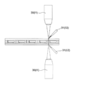
- FIG. 3 is an enlarged view of the cutting process I, and the cutting is performed by irradiating the infrared laser 30 and spraying water on the irradiation position with the water injection device 31. Then, it is cut into individual modules in a later process.
- FIG. 2 is a schematic diagram and shows a module that is separated into pieces instead of a fixed-size sheet.
- the cutting device composed of the infrared laser 30 and the water jet device 31 is configured to be movable integrally in a slightly oblique direction from the sheet width direction, and cuts the sheet while moving in this direction as the sheet is conveyed. Since the sheet is also moved, the sheet and the cutting device are relatively stationary by moving the infrared laser 30 and the water injection device 31 obliquely in the width direction. In addition, as shown by the arrow, the cutting device is configured to be movable in the contact / separation direction with respect to the sheet in order to adjust the focal position of the infrared laser.
- the back surface sealing sheet 3, the surface sealing sheet 4, and the spacer 6 are formed of an inorganic material, cracks generated in the surface sheet due to thermal expansion and contraction due to infrared laser irradiation and water cooling are also present in the spacer. Since it propagates and further propagates to the back sheet 3, laser cutting may be performed only from one side. However, when the spacer 6 is made of resin, the laser is emitted from both sides of the sheet as shown by dotted lines in FIG. Cutting may be performed.
- the sheet may be wound on a roll and separated into separate pieces, or further cut into both the width direction and the conveying direction to be separated into pieces.
- the individualized LED module 1 is completed through an electrode drawing process (not shown).
- the conductive ink is applied and dried on this portion, and the soldering surface is formed to complete the LED module 1.
- the cut LED modules 1 can be aligned in the same direction, and thus the electrode cut surfaces of a large number of LED modules can be formed.
- the conductive ink is applied together, dried and solidified as it is, and the electrode can be drawn out very efficiently.
- the number of electrodes is large, not two, the distance between the electrodes is short, so that a soldering portion for wiring can be formed by adhering metal leads with a conductive adhesive.
- Sheet material As a sheet material used for the front surface sealing sheet and the back surface sealing sheet, there are three types of materials, plastic, glass, and metal.
- Plastic materials include polyethylene, polycarbonate, cycloolefin, and acrylic.
- the thickness of the sheet material is about 1 ⁇ m to 1 mm. Since the optical semiconductor element module is formed in a matrix on the sheet material, the width is preferably about 300 mm, although it depends on the size of the optical semiconductor element module to be manufactured. If the width is too wide, the manufacturing equipment for maintaining high accuracy becomes expensive, and if the width is narrowed, the yield decreases.
- plastic sheet material is thin and excellent in heat dissipation, so it can be brighter than conventional plastic molding sealing, but many plastic materials themselves have heat resistance around 150 ° C and thermal conductivity Since it is low, it is not very suitable for high brightness applications. However, it is suitable for an inexpensive LED for display.
- the glass sheet As for the glass sheet, a sheet material having a thickness of 500 ⁇ m or less is already on the market in the form of a roll, and by using this, high heat resistance of the sheet can be secured and it can be used for high-luminance LED applications. Moreover, since this glass sheet is thin, the surface area per volume is large and the heat dissipation effect is large. Furthermore, if a material with high heat resistance such as low melting point glass is used for the spacer material, all materials constituting the LED module can be made of inorganic materials, so that the heat resistance is remarkably improved and not only suitable for high brightness applications. In the manufacturing process, since the drying / curing treatment can be performed at a high temperature of about 300 ° C., a highly reliable LED module can be manufactured.
- FIG. 4 shows the structure of the LED module 100 in this case. That is, the back surface sealing sheet 3 is a metal sheet, the p-side electrode 5p is formed on the metal sheet, and the insulating layer 10 is first formed on the n-side electrode 5n, and then the n-side electrode 5n is formed thereon. Is forming. Then, a separately manufactured LED chip 2 is turned on.
- the spacers 6a and 6b, the front side sealing sheet 4, and the phosphor 7 are the same as those in FIG.
- the entire mounting surface of the LED chip is in contact with a metal excellent in heat conduction, so that heat generated by light emission can be efficiently diffused to the sheet, and the semiconductor chip itself is prevented from being heated to high temperature. It is the most suitable sheet material for the LED module of the application.
- the loading surface of the LED chip and the metal sheet are tightly bonded by a conductive adhesive and are electrically connected.
- magnesium oxide, barium sulfate, titanium dioxide, or the like can be used, and these exhibit a reflectance of 95 to 99% or more over almost the entire region of visible light.
- Good white material These powders are mixed into the sheet raw material, and a plastic white sheet can be produced by a method such as melt stretching by heating or volatile solidification from solvent melting. Similarly, in the case of a glass sheet, a white sheet can be generated by melt drawing.
- the reflectance is slightly low, around 90%, but a white raw material that is easily clouded and can be applied to the present invention is used. Obtainable.
- the white sheet In the white sheet, light is scattered and reflected in all directions regardless of the incident direction, but in the case of a metal sheet, it is reflected in the same reflection angle direction as the incident angle of light in the form of a mirror.
- the blue reflectance is as low as 60% or less, so a surface such as silver or tin is previously coated on the surface on which the white or blue LED chip is placed.
- the reflectance can be improved by replacing the white reflection instead of the mirror reflection by a method such as applying the above-described white material to the surface of the semiconductor chip stacking side, but the thermal conductivity is slightly deteriorated.
- the adhesion of the electrode to the binder resin material and spacer resin material is greatly increased. This is preferable because it can prevent the peeling and cracking of the joint due to solder reflow or aging, and can improve the manufacturing yield and the reliability of the completed LED module.
- the adhesion of the electrode to the resin material or spacer material is dramatically improved.
- the yield and the reliability of the completed LED module can be improved, which is preferable.
- the silane coupling agent may be difficult to adhere.
- the SiO 2 coat is applied in advance and then the treatment with the silane coupling agent is performed. Just do it.
- the electrode can be formed by sheet screen printing, intaglio printing, or flexographic printing technology in which conductive ink is copied from the relief printing.
- the electrode material is supplied from the outside of the roll plate, but rotary screen printing in which the electrode material is supplied from the inside of the roll plate can also be used. Since such roll screen printing can be continuously performed without intermittent driving such as stopping and re-driving of sheets, an equipment such as an accumulator for taking the sheet feeding timing is unnecessary, and it is a simple and reliable process. So good.
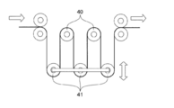
- the accumulator shown in FIG. 5 since intermittent driving such as stopping and re-driving of the sheet is required, the accumulator shown in FIG. 5 is used.
- the accumulator has a configuration in which a plurality of fixed rollers 40 and dance rollers 41 are alternately arranged, and a sheet material is alternately applied to each of the rollers. By moving the dance rollers 41, the speed on the carry-in side and the carry-out side can be increased. It can be changed or stopped. Since the electrode formation is the first step, this accumulator is arranged after the electrode formation step B, the driving of the supply roll is stopped, and the sheet is stopped. Then, an electrode is formed on the stationary sheet by sheet screen printing.
- the subsequent steps are transported at a constant speed, but the speed difference is absorbed by the accumulator. If it is desired to stop the sheet in the middle of the process, two accumulators may be provided, and a necessary process may be arranged between them.
- the electrode material conductive ink, conductive adhesive, or transparent conductive ink
- the electrode material conductive ink, conductive adhesive, or transparent conductive ink
- an electrode is previously formed on the sheet material, and the sheet with the electrode can be used in the manufacturing method of the present invention.
- the electrode forming step B in FIG. 2 can be omitted.
- Electrode material As the electrode material, conductive ink, conductive adhesive, and transparent conductive ink can be used, which will be described in order.
- the conductive ink contains silver particles and graphite as fillers.
- the thickness is 20 ⁇ m and the surface resistivity is 40 to 70 m ⁇ / cm 2.
- the heating condition is about 80 ° C. for about 30 minutes. For this reason, in the above-mentioned embodiment, it is not dried immediately after electrode printing, but is heated and dried in the first drying step E and the second drying step G.
- the binder of the conductive ink can have a relatively high viscosity when a UV curable resin is used, and the printing thickness can be reduced to about 10 to 20 ⁇ m.
- the viscosity of a binder such as a ketone or alcohol is low.
- the printing thickness is about half of about 6 to 10 ⁇ m.
- a weak ultraviolet light is irradiated to make the conductive ink in a semi-cured state. Send to process.
- Conductive adhesive Since the semiconductor chip and the electrode are directly joined in the post-process of electrode printing, the use of an ink imparted not only with conductivity but also adhesion may ensure more electrical joining.
- a conductive adhesive also uses silver particles as a filler, and one-component epoxy, phenol, polyimide, or the like is used as a resin binder.
- This conductive adhesive has a volume resistivity of 5 to 80 ⁇ 10 ⁇ 5 ⁇ ⁇ cm (approximately 0.05 to 0.8 ⁇ / cm 2 in terms of uniform surface resistivity) by heating and drying, and the conductivity of (1). The same resistance value as that of the conductive ink can be obtained.
- the drying and curing conditions are somewhat high, such as 150 ° C. for 30 minutes to 180 ° C. for 60 minutes (one component epoxy, phenol) and 290 ° C. for 20 minutes (polyimide).
- 150 ° C. for 30 minutes to 180 ° C. for 60 minutes one component epoxy, phenol
- 290 ° C. for 20 minutes polyimide
- Transparent conductive ink There are inks that are made transparent by using ITO fine particles, organic In-Sn, monodispersed Au-Ag, Ag nanoparticles, etc. as the filler of the conductive ink.
- the electrode can be generated by printing on the front side of the white sheet in the same manner as the conductive ink and the conductive adhesive.
- the LED light emitted to the white reflective sheet side was absorbed by the electrode, but it was transmitted by the transparent electrode and reached the white sheet, where high efficiency was achieved. After being reflected, the light passes through the transparent electrode and is returned to the LED chip, thereby contributing to an improvement in the intensity of the emitted light from the LED.
- This transparent conductive ink also needs to be dried by heating after printing. Temperature conditions of 120 ° C. are necessary for ITO fine particles, monodispersed Au—Ag and Ag nanoparticles, and 450 ° C. for organic In—Sn. Also, since the viscosity of the ink is generally low, the printed thickness is often thin, but the surface resistivity is slightly high at 0.05 to 2 ⁇ / cm 2 at a thickness of about 5 ⁇ m. By appropriately selecting the viscosity of the transparent conductive ink, it is possible to respond to commercially available products from low-viscosity ink printing such as gravure (intaglio printing) and inkjet printing, and high-viscosity screen printing.
- low-viscosity ink printing such as gravure (intaglio printing) and inkjet printing, and high-viscosity screen printing.
- the transparent conductive ink printed on the electrodes is semi-cured under a short heating condition for a short time and continuously sent to the next step.
- the LED module 110 When the electrode is arranged on the transparent sheet, that is, when the electrode is printed on the transparent sheet on the side where the LED light is emitted, a transparent conductive ink is used.
- the configuration of the LED module 110 in this case is shown in FIG.
- the LED module 110 first, the LED chip 2 is placed between the spacers 6a and 6b formed on the back surface sealing sheet 3, and the n-side electrode 5n and the p-side electrode 5p are made of transparent conductive ink thereon. Is formed by laminating and bonding the transparent front side sealing sheet 4. Alternatively, the n-side electrode 5n and the p-side electrode 5p may be formed on the transparent surface sealing sheet 4 in advance, and these may be laminated and bonded.
- the LED module 110 directly bonds the LED chip 2 to the electrodes 5n and 5p, there is no room for sandwiching the phosphor, and functions such as emission wavelength conversion using fluorescent light, increase in light quantity, and improvement in hue cannot be realized. This is for an LED module that emits the emission wavelength of the LED as it is.
- an offset gravure method is employed for the spacer forming step, but an inversion method in which printing is performed after removing an unnecessary spacer material in a semi-cured state with a relief printing plate may be used.
- a thick film can be formed relatively easily, so that it is more preferable for spacer printing.
- the creation of the spacer is also preferable because the spacer thickness can be increased by molding a UV curable resin or molding by thermal curing such as low melting point glass.
- Spacer material As the spacer material, a glass material such as gel glass or a low melting point glass paste, or an energy curable resin such as a thermosetting resin or a UV curable resin can be used.
- Low melting point glass paste uses frit glass (flakes or powdered glass blended with natural and industrial raw materials such as silica sand, feldspar, lime, etc., melted at high temperature, quenched and ground) Borosilicate glass or aluminosilicate glass that was made into a paste with water or solvent. A slightly softer slurry may be used. When this is continuously printed as an ink on a sheet and dried, it solidifies in a clay state and is sent to a subsequent process in this state.
- the glass is sintered into a dense glass body.
- the curing and sealing conditions are 400 to 450 ° C. for 10 minutes, and the sheet material is limited to glass or metal due to the high temperature, and the linear expansion coefficient is adjusted to prevent cracks due to differences in thermal expansion and contraction.
- the low-melting glass has a linear expansion coefficient ranging from 3 to 12 ppm, and can be selected as appropriate.
- Thermosetting resin or UV curable resin A spacer can also be continuously formed on a sheet with a thermosetting resin or a UV curable resin.
- a resin material bakelite, an epoxy resin, or an acrylic resin is usually used. However, since the heat resistance is 280 ° C. or higher, the resin material has reflow resistance and can withstand a drying / baking process below this temperature.
- the formed spacer is made into a semi-cured state and sent to the next step.
- the semi-cured state in the thermosetting resin, the curing heating conditions such as temperature and time are loosened, and in the UV curable resin, the UV is cured. This can be achieved by reducing the amount of irradiation.
- Complete curing is performed by heating or UV irradiation in a process after the mounting of the semiconductor chip or phosphor. This is because when the semiconductor chip and phosphor are mounted and sealed with a transparent sheet, if the spacer is pressed in a semi-cured state, the spacer material wets the transparent sheet and adhesion is increased. This is because the spacer is completely cured to improve hermeticity and certainty of sealing.
- the phosphor can be applied by a technique such as a droplet method in which a phosphor turbid liquid is dropped or an ink jet method. Also in this case, since the phosphor does not dissolve in the solvent, the solution is always put in a stirring state and applied while preventing precipitation or uneven distribution.
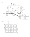
- FIG. 7 is a schematic view showing a modified example of the phosphor spray application.
- a mask for not applying the phosphor to unnecessary portions is made endless and continuously used and the phosphor is recovered.
- the mask 50 is formed in an endless belt shape using a stainless sheet or the like, and a plurality of openings are formed in a matrix shape in a portion where the phosphor is applied (see FIG. 7B).
- the spray 51 disposed inside the mask 50 may reciprocate in the width direction to apply the phosphor, or may be a line spray. After spray application, the mask 50 passes through a cleaning container 52 containing a solvent to wash off the phosphor, and then returns to the spraying process through a drying process by the infrared lamp 53.
- Phosphors have a very high specific gravity of about 3 to 5 and are insoluble in water, so the belt with the phosphors attached is peeled off and precipitated simply by soaking it in water or solvent. And can be reused. Since the phosphor is expensive, the phosphor can be applied at low cost by washing and collecting in this manner.
- the droplet method is a method in which a turbid liquid of phosphor is dropped at a desired position.
- a turbid liquid of phosphor is dropped at a desired position.
- the amount of the phosphor is adjusted by changing the size of the droplet depending on the outlet thickness of the syringe to be dropped and the number of drops.
- the glass sheet which is a transparent inorganic material is laminated and bonded, but a transparent plastic sheet can also be bonded by pressure bonding with a heating roller.
- sealing can be performed by applying a transparent plastic material or a transparent inorganic material.
- a transparent plastic material such as PET dissolved in methyl chloride or chloromethane.
- Application may be spray or roll printing, but the thickness of the plastic layer created by a single application is several ⁇ m, so repeated application and drying are repeated to increase the thickness of the plastic layer. Ensure sealing.
- PHPS all side chains are hydrogen
- the polysilazane) is dissolved in an organic solvent such as xylene and butyl ether. By containing an amine catalyst, it is dried and solidified even at room temperature to produce a dense glass layer of SiO 2 .
- a solvent containing moisture such as alcohol cannot be used.
- Such a polysilazane material can be sealed by being applied onto the LED chip on the sheet by spraying or coating, and then dried and cured. Furthermore, the phosphor is turbid in the polysilazane solvent, spray coated with a thickness of several tens of ⁇ m on the LED chip while stirring so as not to precipitate, and then dried and volatilized to form a dense glass seal containing the phosphor. Can do. That is, the phosphor coating process and the sealing process can be combined into one.
- the thickness of the glass generation layer by a single application of polysilazane is about several ⁇ m, and although it is a dense glass layer, its strength is weak and the sealing may be damaged. Repeated application and drying increase the thickness. And good. These multiple times of application
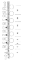
- FIG. 8 schematically shows a sealing process by polysilazane coating.
- the chip-on process D the first drying process E, the phosphor coating process F, and the second drying process G.
- three times of polysilazane spray coating are performed.
- drying by irradiation with an infrared lamp steps H1, H2, and H3.
- the irradiation light amount of the infrared lamp is adjusted so that the next coating step is started before the drying is completed. This is to avoid the occurrence of a clear boundary in the glass layer generated by coating, which causes cracks and peeling.
- the glass layer that has been laminated and applied is further integrated by heating to 200 to 250 ° C. with an infrared lamp (step H4) to further increase the denseness.
- the sealing process by the second sheet is not necessary, so the process is simplified, the equipment and the cover material are not required, the cost is low, and the yield can be improved. High quality LED products can be obtained stably.
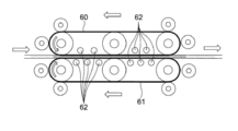
- the heating after sealing can be performed in a state of being sandwiched between endless belts 60 and 61 shown in FIG. 9 instead of a heating roller or an infrared lamp.
- Each of the two endless belts 60 and 61 is stretched around three rollers, and a pressing roller is disposed on the outer periphery of the belt.
- a plurality of heaters 62 are provided inside the endless belts 60 and 61, and the heat of the heaters 62 is applied to the sealed sheets via the endless belts 60 and 61. Since this heating method heats the sheet while pulling it straight, an optical semiconductor element module with high dimensional accuracy can be produced without bending.
- Cutting in the conveyance direction can be performed while carrying the infrared laser beam by the number of semiconductor modules arranged in the width direction, but cutting in the width direction requires maintaining the relative position of the laser cutting device and the sheet stationary. is there.
- the relative stationary method can be realized by the following two methods.
- A This is a method in which an accumulator is installed before the sheet feeding cutting process to allow extra time to wind up the sheet with a dance roller, and the sheet feeding in the laser cutting process is stopped during that time.
- the accumulator can have the above-described configuration.
- the laser cutting described above uses water for rapid cooling, so a drying process is required. By cutting the work directly into the pure water cleaning process after cutting, the drying process after cutting is unnecessary. Can do.
- the sheet on which the semiconductor chip is loaded uses a copper sheet to improve thermal conductivity, copper is difficult to cut with an infrared laser because of its high infrared reflectance, so an absorbent material is applied. It can be easy to keep.
- FIG. 10 schematically shows this cutting method.
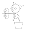
- a band-shaped blade 71 is set on the drum surface of the rotary die 70, and the rotary die 70 and the bearer 72 are rotated in synchronization with sheet feeding. Cutting can be realized with an accurate dimension of the cut blade 70.
- the illustrated example is an example in which a blade is provided only in the width direction of the sheet.
- the semiconductor modules are cut into a line and separated into individual pieces.
- each semiconductor module can be separated into individual pieces. In this case, it is also necessary to have a configuration for winding the punched residue.
- the manufacturing method of the optical semiconductor element module of the present invention can greatly increase the production efficiency as compared with the conventional method.
- the number of LED modules that can be completed with one molding machine or sealing device is about 20 million pieces / year for resin sealing, and about 1/10 of that for glass sealing.
- the number of LED modules that can be manufactured by one unit per year is 7.29 billion / year. This calculation is based on a printing roll plate diameter of 120 mm, width of 300 mm, feed speed of 1 m / min, LED module size of 4 mm square, and device operation rate of 75%. Absent.
Landscapes
- Engineering & Computer Science (AREA)
- Manufacturing & Machinery (AREA)
- Led Device Packages (AREA)
Abstract
一方面の封止材となる連続シートを搬送し、連続シートの搬送方向に順に、連続シート上に電極を形成する工程、スペーサーを形成する工程、スペーサーの間に別途製作した光学半導体素子チップをチップオンする工程、他方面の封止材を供給して封止を行う工程、を配置して複数の光学半導体素子モジュールを形成したシートを作成する。
Description
本発明は、光学半導体素子モジュールの製造方法に関する。光学半導体素子は、LED(無機LED、有機LED=有機EL)、CCD画像センサー、CMOS画像センサー等を含み、発光、または受光の光学機能を行う半導体素子であり、これらの素子チップに電極などを形成してモジュール化した光学半導体素子モジュールの製造方法に係わる。
従来、これらの光学半導体素子、例えばLEDモジュールの製造方法は、単結晶基板上にエピタキシャル成長により半導体を形成し、これを個別の素子にする分割溝を形成し、必要箇所に電極パッドを形成してチップ化する。そして、この電極パッドに電極をワイヤボンディングし、樹脂などでの封止によってモジュール化し、最後にパッケージングを行って完成するという製造方法が一般的であった(例えば、特許文献1参照)。
チップ化は、形成した半導体に対して、フォトリソ技術、エッチング技術による、分割溝の形成、電極パッドの形成、必要に応じ(透明)電極の形成を実施することで行われる。このようなチップ化とワイヤボンディングを行った後、先に個別の素子に切断してから封止するか、あるいは封止を行ってから切断する場合がある。
光学半導体素子の製造には、素子の機能に応じて各種の変形や改良があるが、基本的には上記のような工程で行われる。
切断してから封止を行う製造工程をさらに具体的に説明すると、従来は、500個分程の配線を打ち抜いて連ねた銅板上に、半導体チップを一つ一つ載せてワイヤボンディングにより電極パッドと配線とを繋ぎ、樹脂封止の場合は熱硬化性樹脂のトランスファー成形装置に投入し、10分程の時間をかけて樹脂を射出し封止していた。
また、高輝度LEDでは、発熱が大きいのでガラス封止となるが、ガラス成形により1分/個程で成形されたガラス基板に一つ一つ半導体チップや蛍光体を埋設して、最後はガラス板で蓋をして低融点ガラスで封止する方法が取られていた。
従って、1台の成形装置や封止装置で完成できるLEDモジュールの数は、樹脂封止で大凡2000万個/年程であり、ガラス封止ではその1/10程度となる。封止を行ってから切断する場合においても上記とほぼ同程度の生産量となる。
このように従来の製造工程は、それぞれの工程を異なる装置によって行わねばならないので、生産効率が悪いという欠点がある。半導体を成長させる工程は真空蒸着装置やCVD装置を用いなければならないが、それ以降の工程は創意工夫により連続化ができる可能性があり、このように工程の連続処理が可能となると、生産効率を大幅に向上させることができる。
特に封止工程については、従来では、封止材料としてシリコーン樹脂やガラスが用いられてきたが、封止において前者は接着剤が付きにくく硬度が低い欠点があり、後者は部品だけでなく封止工程の生産性も悪いために高価になるという課題があった。
また、LEDチップなどの場合は熱の問題がある。LEDチップは電力から光への変換効率は高いが、それでも高輝度にするために電流を増やすと変換損失分の熱が多量に発生する。しかも、LEDチップは寸法が小さいため熱容量が小さく、発光部分はさらに小さな部分であるため、発光とともに非常に小さい領域に集中して熱が発生するので、数100℃の高温になり易い。従って、LEDチップを封止する部分は、耐熱性が高く放熱性の良い(熱伝導が良く表面積が大きく体積が小さい)材料と形態のものが、投入電流を増やせ、より高輝度に発光できるので有利である。
ところが、従来の樹脂やガラスによる封止材料は、いずれも熱導電性が悪い材料であり、成形によって形成しているため厚肉で熱容量が大きく、従って放熱性が悪かった。樹脂材料では耐熱性が高くないため、黄色に変色したりして高輝度用途には向かず、またガラス材料では耐熱性はあるが、発生する熱が逃げないため半導体チップの温度が容易に上昇し、チップの焼損を免れるために大電流を供給できないという問題があった。即ち、従来の封止材料では、樹脂のみならずガラスであっても、高輝度化には封止による限界があったことと、特にガラス材料では生産性が非常に悪いため高価であり、車のヘッドランプなどの用途に限定されていた。
従って、従来の樹脂材料による封止では、長時間の点灯により透過率の低下が観察され、特に青色付近の透過率が容易に80%を下回る状態であった。透過率低下分の20%のうち、9%はカバー表裏面における表面反射損失で、反射防止コートなどで改善することは可能であるが、コストがかかるため通常は行わない。残り11%の低下分が、材料の吸収によるものであり、熱や被曝による劣化が原因で発生する。
本発明は、以上のような課題を解決すること、すなわち製造工程の改良により生産効率を高めることを目的とする。
本発明は、さらに製造工程の改良と封止材料の改良を図り、以って熱伝導性や耐熱性の面で優れた封止材料を用いることのできる製造工程を提供することを目的とする。
上記の目的は、一方面の封止材となる連続シートを搬送し、該連続シートの搬送方向に順に、前記連続シート上に電極を形成する工程、スペーサーを形成する工程、前記スペーサーの間に別途製作した光学半導体素子チップをチップオンする工程、他方面の封止材を供給して封止を行う工程、を配置して複数の光学半導体素子モジュールをその上に形成したシートを作成することによって達成される。作成されたシートは、その後切断して個別の光学半導体モジュールとされるが、この切断工程を封止工程の後に配置しても良い。
このように、連続シート上に順次光学半導体素子モジュールを構成する部材を順次形成して行く製造方法であるので、極めて高い生産性と低コスト化、および品質の高信頼性を実現することができるのである。
封止材料としては、シート状の材料を積層接着してもよく、また液状の材料を塗布乾燥させてもよいが、いずれにおいても、薄い封止膜となるように材料または工程を構成する。封止膜の薄さは、10μm~1000μm、より好ましくは10μm~500μmである。高輝度化のため駆動電流を大きく使えるように、熱の放熱をよくする必要があるが、あまり厚い封止材料では熱が蓄積されてしまうので、薄い方が良い。また、封止材料がシート状でロールに巻いたりする場合には、シート厚が1mm以下でないとプラスチックやガラス材料では折れたり変性したりするし、金属材料では皺が入ったりする。さらに500μm以下とすれば、これらの欠陥が生じない充分な柔軟性を確保できるので、より好ましい。しかしながら、封止材料の厚みを10μm以下まで薄くすると、強度的に弱いため容易にクラックが入って封止が破れる心配があるので、10μm以上とするのが好ましい。
本発明では、これら封止材料の形態を薄いシート材料や塗布材料としたため、熱が蓄積しにくく放熱性も良いので、従来と同じLEDチップを使用しても、より多くの電流を投入でき、もって高輝度化が実現でき、出射光の封止材料を通る透過光路長が短いので樹脂材料による封止の場合でも色味の変化が少ないという大きな改善効果が得られる。
さらに具体的には、本発明の目的は、以下に記載の製造方法によって達成できる。
1.複数の光学半導体素子チップをモジュールに連続して形成する光学半導体素子モジュールの製造方法であって、モジュールの一方面の封止材となる連続シートを搬送し、該連続シートの搬送方向に順に、前記連続シート上に前記光学半導体素子チップと接続される電極を形成する電極形成工程、各チップの境界となり、厚みを規制するスペーサーを形成するスペーサー形成工程、前記スペーサーの間に光学半導体素子チップをチップオンするチップオン工程、前記光学半導体素子チップ上に他方面の封止材となる封止材料を供給して封止を行う封止工程、を配置して複数の光学半導体素子モジュールを形成したシートを作成することを特徴とする光学半導体素子モジュールの製造方法。
2.複数の光学半導体素子チップをモジュールに連続して形成する光学半導体素子モジュールの製造方法であって、前記光学半導体素子チップと接続される電極をあらかじめ表面に形成され、モジュールの一方面の封止材となる連続シートを搬送し、該連続シートの搬送方向に順に、各チップの境界となり、厚みを規制するスペーサーを形成するスペーサー形成工程、前記スペーサーの間に光学半導体素子チップをチップオンするチップオン工程、前記光学半導体素子チップ上に他方面の封止材となる封止材料を供給して封止を行う封止工程、を配置して複数の光学半導体素子モジュールを形成したシートを作成することを特徴とする光学半導体素子モジュールの製造方法。
3.前記封止工程の後に、複数の光学半導体素子モジュールを形成したシートを切断する工程を含むことを特徴とする前記1または2に記載の光学半導体素子モジュールの製造方法。
4.前記封止材が、樹脂材料、ガラス材料、もしくは金属材料のいずれかであることを特徴とする前記1から3のいずれかに記載の光学半導体素子モジュールの製造方法。
5.前記封止材の厚みが、10μm~1000μmであることを特徴とする前記1から4のいずれかに記載の光学半導体素子モジュールの製造方法。
6.前記封止材の厚みが、10μm~500μmであることを特徴とする前記1から4のいずれかに記載の光学半導体素子モジュールの製造方法。
7.前記封止工程が、シート材を積層・接着する工程であることを特徴とする前記1から6のいずれかに記載の光学半導体素子モジュールの製造方法。
8.前記封止工程が、30℃以上でスペーサー材料のガラス転移点以下の温度で加熱する加熱手段を含むことを特徴とする前記7に記載の光学半導体素子モジュールの製造方法。
9.前記封止工程が、少なくとも1kg/cm2以上で加圧する加圧手段を含むことを特徴とする前記7に記載の光学半導体素子モジュールの製造方法。
10.前記モジュールの一方面の封止材となる連続シートに電極を形成する前に、もしくは前記他方面の封止材となる封止材料がシート材であって、該シート材で封止を行う前に、当該シート材にシランカップリング材を塗布することを特徴とする前記7に記載の光学半導体素子モジュールの製造方法。
11.前記シート材にシランカップリング材を塗布する前にSiO2コートを施すことを特徴とする前記10に記載の光学半導体素子モジュールの製造方法。
12.前記封止工程が、封止材を塗布する工程であることを特徴とする前記1から6のいずれかに記載の光学半導体素子モジュールの製造方法。
13.前記封止工程において、塗布する封止材が、透明プラスチック材料、もしくは透明無機材料であることを特徴とする前記12に記載の光学半導体素子モジュールの製造方法。
14.前記封止工程において、塗布する封止材が、ポリシラザンであることを特徴とする前記13に記載の光学半導体素子モジュールの製造方法。
15.前記スペーサー形成工程が、スペーサーを印刷、もしくは成形によって形成することを特徴とする前記1から14のいずれかに記載の光学半導体素子モジュールの製造方法。
16.前記スペーサー形成工程が、スペーサー材料を半硬化させた状態で次工程に送ることを特徴とする前記1から15のいずれかに記載の光学半導体素子モジュールの製造方法。
17.前記スペーサー形成工程におけるスペーサー材料が、ゲルガラス、低融点ガラス、エネルギー硬化性樹脂のいずれかであることを特徴とする前記16に記載の光学半導体素子モジュールの製造方法。
18.前記電極形成工程における電極材料が、導電性インク、透明導電性インク、導電性接着剤のいずれかであって、該電極材料を印刷によって連続シート上に形成することを特徴とする前記1から17のいずれかに記載の光学半導体素子モジュールの製造方法。
19.前記光学半導体素子チップがLEDチップであることを特徴とする前記1から18のいずれかに記載の光学半導体素子モジュールの製造方法。
20.前記チップオン工程の後に、前記LEDチップの発光光を波長変換するための蛍光体をLEDチップ上に積層する蛍光体塗布工程を有することを特徴とする前記19に記載の光学半導体素子モジュールの製造方法。
21.前記蛍光体塗布工程が、無端ベルト状のマスクを介して蛍光体をLEDチップ上に塗布するとともに、蛍光体塗布後に前記マスクを洗浄、乾燥させることを特徴とする前記20に記載の光学半導体素子モジュールの製造方法。
22.前記蛍光体塗布工程において、前記マスクを洗浄した後、洗い落とされた蛍光体を回収して再利用することを特徴とする前記21に記載の光学半導体素子モジュールの製造方法。
23.前記蛍光体塗布工程が、ポリシラザンに蛍光体を混濁した混濁液を前記LEDチップ上に塗布することによって前記封止工程を兼用することを特徴とする前記20に記載の光学半導体素子モジュールの製造方法。
本発明は、極めて高い生産性と低コスト化、および品質の高信頼性を実現することができる。
また、封止材料の形態を薄いシート材料や塗布材料としたため、熱が蓄積しにくく放熱性も良いので、熱伝導性や耐熱性の面で優れた光学半導体素子モジュールを提供できる。
本発明によって製造できる光学半導体素子モジュールは、LED(無機LED、有機LEDまたは有機EL)、CCD画像センサー、CMOS画像センサー等があり、これらの素子チップに電極などを形成してモジュール化したものである。
以下、本発明を図を用いて説明する。図1(a)は本発明によって製造された光学半導体素子モジュールの一例であるLEDモジュール1を示しており、内部に別途製作されるLEDチップ2を有している。LEDモジュール1は、その裏側(図の下側)に白色反射ガラスシートからなる裏面封止シート3と、その表側に透明ガラスシートからなる表面封止シート4とで挟みこまれている。
裏面封止シート3の上には、n側電極5nとp側電極5pが形成されており、n側電極5nとp側電極5pにLEDチップ2が載置され、それぞれの電極パッドと接続されている。また、LEDチップ2の両側には、チップの境界となり厚みを規制するスペーサー6a、6bが設けられ、裏面封止シート3と表面封止シート4とで四周を囲む形態となっている。図は縦断面を示すが、横断面においても四周が囲まれる構造である。これら四周を囲む構造とLEDチップ2との隙間は、蛍光体7で埋められており、LEDチップ2の光と蛍光体7の光との混合により所望の色の光を発生するようになっている。例えば、LEDチップ2の発光色を青色とし、蛍光体7の発光色を黄色とすると、補色関係にある青と黄の混合で白色の発光を得ることができる。
図1(b)は、LEDチップ2の構造を示す図である。LEDチップ2は、サファイア基板21の上に透明電極22、n型GaNのクラッド層23、発光層24、p型GaNのクラッド層25、透明電極26が順次積層されており、透明電極22と透明電極26の上には、それぞれn側電極パッド27、p側電極パッド28が形成される。
このようなLEDチップ2は公知の製造方法で製造され、後述する工程でチップオンされる。図1(a)に示すLEDモジュール1は、LEDチップ2を図1(b)の状態からさかさまにして載置する、いわゆるフリップチップ接続タイプである。LEDチップ2は、表側と裏側の両方から発光するが、図1(b)で裏側、すなわちサファイア基板21側からの発光を主に使う。表側からの発光は、n側電極5nとp側電極5pで覆われない部分からの光が裏面封止シート3で反射されてLED発光の一部をなす。n側電極5nとp側電極5pを透明電極とした場合は、これら電極を透過して裏面封止シート3で反射された光もLED発光に寄与できる。
次に、本発明の光学半導体素子モジュールの製造方法を、上記LEDモジュールの製造を例にとって説明する。図2は、この製造方法の工程を示す模式図である。
実施の形態における各工程は、
・モジュールの一方面の封止材となる連続シートを搬出するシート搬出工程A、
・連続シート上にLEDチップと接続される電極を形成する電極形成工程B、
・各チップの境界となり厚みを規制するスペーサーを形成するスペーサー形成工程C、
・スペーサーの間に別途製作のLEDチップをチップオンするチップオン工程D、
・第1乾燥工程E、
・LEDチップ上に蛍光体を塗布する蛍光体塗布工程F、
・第2乾燥工程G、
・他方面の封止材となる封止材料を供給して封止を行う封止工程H、
・シート上に形成された各モジュールを切断して個片化する切断工程I、
とを基本とする。
・モジュールの一方面の封止材となる連続シートを搬出するシート搬出工程A、
・連続シート上にLEDチップと接続される電極を形成する電極形成工程B、
・各チップの境界となり厚みを規制するスペーサーを形成するスペーサー形成工程C、
・スペーサーの間に別途製作のLEDチップをチップオンするチップオン工程D、
・第1乾燥工程E、
・LEDチップ上に蛍光体を塗布する蛍光体塗布工程F、
・第2乾燥工程G、
・他方面の封止材となる封止材料を供給して封止を行う封止工程H、
・シート上に形成された各モジュールを切断して個片化する切断工程I、
とを基本とする。
シート搬出工程Aでは、裏面封止シート3をロール状に巻いたロールシートを搬送装置にセットし、裏面封止シート3を後工程まで引き伸ばす。用いる裏面封止シート3は、厚さ500μm、幅の300mmの白色ガラスシートで、送り速度は1m/minとした。
電極形成工程Bは、裏面封止シート3上にn側電極5nとp側電極5pとを形成する工程である。本実施の形態で用いる電極材料は、導電性インクで、バインダーとしてUV硬化樹脂を用い、ロールスクリーン印刷装置B1によって電極形成した後、弱い紫外線光を照射する紫外線照射ランプB2によって半硬化の状態とした。半硬化とするのは、後の工程でチップオンするLEDチップ2の電極パッドとの接着性を向上させるためである。
スペーサー形成工程Cは、LEDチップを載置する境界となり厚みを規制するスペーサーを形成する工程である。ここでは、低融点ガラススラリーをオフセットグラビア印刷装置C1で所望の形状に印刷する。印刷したスペーサーは、半硬化状態にして次工程に送る。
ここでいう半硬化状態とは、完全硬化した時の樹脂の場合の押し込み硬度に対して半分以下の硬度を有する状態を指す。この状態では、粘度は非常に高いが流動性はまだ残っている状態であるため、加圧されると相手側の材料に対して、樹脂が流れ出すことなく濡れることができる。また、加圧に際しては、粘度を低下させてより濡れやすくするために、加熱も併用するとより確実で効果的である。加熱は半硬化状態や保持時間にもよるが、適宜選択することで30℃と室温よりわずかに高くするだけでも、濡れ性が大きく改善する場合がある。封止時の加圧によってスペーサーが変形しては意味がなくなるため、加熱温度は樹脂の場合ではガラス転位点より高くすることは不適当である。
低融点ガラススラリーの場合は、半硬化状態とは、溶剤が適宜揮発して粘土状になった状態を指す。溶剤を完全に揮発させてしまうと、チョーク状に硬化した状態(グリーン)になるので、この状態では封止材料に対し濡れにくくなってしまうので不適当である。
チップオン工程Dは、別途製造されたLEDチップ2をスペーサーの間に装着する工程である。図示はしていないが、LEDチップ2は、実装する前に電極パッドに導電性インク、導電性接着剤、または透明導電性インクを付着させている。これにより前工程で形成された電極との濡れ性が向上し、強固な連結と良好な電気導通性を得ることができる。LEDチップの実装は、産業用ロボットで行うが、この技術は公知であるので、詳細な説明は省略する。
第1乾燥工程Eは、電極形成工程Bおよびスペーサー形成工程Cで形成された電極とスペーサーが半硬化の状態であるので、これを赤外線ランプE1で乾燥・硬化させる工程である。この工程によって、LEDチップ2はスペーサーの間に固定される。
蛍光体塗布工程Fは、白色発光のLEDとするために蛍光体をLEDチップ2上に塗布する工程である。蛍光体は、溶液に混ぜて攪拌しながらスプレー塗布する。スプレー塗布する際に、塗布する範囲を規制するため、スプレーF1とシートの間にマスクF2を設けている。
第2乾燥工程Gは、蛍光体塗布工程Fで塗布された溶液を蒸発させ、蛍光体を赤外線ランプG1で乾燥・固化する工程である。
封止工程Hは、前工程で蛍光体を塗布乾燥させたモジュールに封止を行う工程である。本実施の形態では、裏面封止にガラスシートを用いたので、表面封止もガラスシートで行う。ここで用いるガラスシートは、発光面側を封止するので、透明のガラスシート4を用いる。透明のガラスシート4をロールから供給してモジュールの表面に積層し、加熱ローラH1による加熱・加圧で接合する。この加熱は、スペーサーが樹脂材料の場合は30℃以上でガラス転移点以下の温度であり、加圧は、少なくとも1kg/cm2以上である。低融点ガラススラリーの半硬化状態では、80℃から200℃間での範囲で加熱して、溶剤を完全に揮発させ硬化固定する。
切断工程Iは、連続シート上に形成されたLEDモジュールを切断する工程である。図3は切断工程Iを拡大して示す図であり、切断は、赤外線レーザー30を照射し、照射位置に水噴射装置31で水を吹き付けることで行い、ここでは、定寸のシートに切断し、後工程で個別のモジュールに切断する。なお、図2は模式図であり、定寸シートでなく個片化されたモジュールを記載している。
赤外線レーザーで局所的に加熱されたガラスに水を吹き付けると、割れが成長・進行して切断を行うことができる。赤外線レーザー30と水噴射装置31からなる切断装置は、シート幅方向から少し斜めの方向に一体的に移動可能に構成され、シートの搬送に従い、この方向に移動しながらシートを切断する。これは、シートも移動しているので、赤外線レーザー30と水噴射装置31を幅方向に斜めに移動させることで、シートと切断装置とを相対的に静止させるのである。なお、切断装置は、矢印で示すように、赤外線レーザーの焦点位置を調整するため、シートに対して接離方向に移動可能に構成される。
本実施の形態においては、裏面封止シート3も表面封止シート4もスペーサー6も無機材料で形成したので、赤外レーザー照射と水冷による熱膨縮で表面シートに発生する割れがスペーサーにも伝搬し、さらに裏面シート3にも伝搬するので、レーザー切断は一方の側からのみでよいが、スペーサー6が樹脂で形成された場合は、図3で点線で示すように、シートの両側からレーザー切断を行うようにすれば良い。
なお、シートを切断することなく、ロールに巻き取り、別工程で個片化してもよく、さらには、幅方向と搬送方向の両方向に切断して一挙に個片化してもよい。
最終的に個片化されたLEDモジュール1は、不図示の電極の引き出し工程を経て完成する。切断工程Iでは、切断面に電極の端面が露出しているので、この部分に導電性インクを塗布・乾燥させ、半田付け面を形成してLEDモジュール1を完成させるのである。
特に透明シート側に集光レンズなどが成形されずシート平面のままの場合は、切断されたLEDモジュール1の向きを揃えて重ねることができ、このようにして多数のLEDモジュールの電極切り口面を揃えて重ねた後に、導電性インクをまとめて塗布し、そのまま乾燥・固化することで、非常に効率よく電極の引き出しができる。また、電極数が2つではなく多い場合は、電極間の距離が短く並ぶため、金属リードを導電性接着剤で接着することで、配線用の半田付け部分を形成することができる。
次に、本実施の形態で用いられる材料、および実施の形態の変形例を説明する。
[シート材]
表面封止シートと裏面封止シートに用いるシート材としては、プラスチック、ガラス、金属の3種類がある。
表面封止シートと裏面封止シートに用いるシート材としては、プラスチック、ガラス、金属の3種類がある。
プラスチック材料としては、ポリエチレンやポリカーボネイト、シクロオレフィン、アクリルなどがある。シート材の厚みは、1μm~1mm程度である。幅は、このシート材の上にマトリクス状に光学半導体素子モジュールが形成されていくので、製造する光学半導体素子モジュールの大きさにも依存するが、300mm程度が好適である。あまりに幅を広くすると精度を高く保つための製造設備が高価になるし、幅を狭くすると、収量が少なくなる。
プラスチック製のシート材による封止は、薄く形態的に放熱性が優れるので従来のプラスチック成形封止よりも高輝度にできるが、多くのプラスチック材料そのものが耐熱性が150℃前後で熱伝導率も低いため、高輝度用途にはあまり適さない。しかし表示用などの廉価版のLEDには好適である。
ガラスシートは、厚みが500μm以下のシート材料がロール形態で既に市販されており、これを使うことによりシートの高耐熱性が確保でき、高輝度のLED用途に供することができる。また、このガラスシートは、薄いため体積当たりの表面積が大きく放熱効果が大きい。さらに、スペーサー材料に低融点ガラスなどの耐熱性の高い材料を用いると、LEDモジュールを構成する全ての材料を無機材料にできるため、耐熱性が格段に向上して高輝度用途に適するばかりでなく、製造プロセスにおいても300℃前後の高温で乾燥・硬化処理ができるので、信頼性の高いLEDモジュールを製造できる。
また、金属シート材料としては、銅やステンレスなどがあり、出射(表)側とは反対(裏)側のシートに使うことができる。この場合はシート材料が導電性のため、LEDモジュールの2つの電極のうちの一方を兼ねて省略できるが、もう一方の電極には絶縁が必要となるので、絶縁層の印刷工程が増える。図4にこの場合のLEDモジュール100の構造を示した。すなわち、裏面封止シート3を金属シートとし、この金属シート上にp側電極5pを形成し、n側電極5nの部分には、まず絶縁層10を形成してからその上にn側電極5nを形成している。そして別途製作されたLEDチップ2をチップオンする。スペーサー6a、6b、表側封止シート4、蛍光体7は図2と同様である。
金属シートを使った構造では、LEDチップの積載面全面が熱伝導に優れる金属に接するため、発光に伴う発熱を効率よくシートに拡散でき、半導体チップそのものが高温化することを防ぐため、高輝度用途のLEDモジュールには最もふさわしいシート材料となる。LEDチップの積載面と金属シートは、導電性接着剤によって密着接合され、電気的にも導通する。
裏面封止シート3のシート材を白色にする白色物質は、酸化マグネシウムや硫酸バリウム、あるいは2酸化チタンなどが利用でき、これらは可視光線のほぼ全領域にわたって95~99%以上の反射率を示す良好な白色素材である。これらの粉体をシート原材料に混入して、加熱による溶融延伸または溶媒溶融からの揮発固化などの方法によって、プラスチックの白色シートを生成することができる。また、ガラスシートの場合も同様に、溶融延伸によって白色シートを生成できる。
プラスチックシートやガラスシートの場合では、屈折率の異なる異種のプラスチックやガラスを混合する方法によれば、反射率は90%前後とやや低いが、容易に白濁して本発明に適用できる白色原料を得ることができる。
白色シートでは、光が入射方向に関わらず全方位に散乱して反射するが、金属シートの場合では、ミラー状に光の入射角と同じ反射角方向に反射する。しかし、金属シート材として、熱伝導に優れる銅を用いると、青色の反射率が60%以下と低いので、白色や青色LEDチップを積載する側の面に予め銀やすずなどのコートを行って青色反射率向上させると、発光輝度が大幅に向上するので良い。また、前述した白色材料を半導体チップの積載側の面に塗布するなどの方法によっても、ミラー反射ではなく白色反射に置き換えられて反射率を向上できるが、熱伝導性はやや劣化する。
また、プラスチックシートのLEDチップの積載側の面に、予めSiO2コートを施した上に、シランカップリング処理を行う工程を設けると、電極のバインダー樹脂材料やスペーサー樹脂材料との密着性が大幅に向上し、半田リフロー時や経年変化などによる接合部の剥離やクラックの発生を予防でき、製造収率や出来上がったLEDモジュールの信頼性が向上できるので好ましい。
同様に、ガラスシートの場合もシート材のチップ積載面側にシランカップリング剤を塗布・乾燥する工程を設けると、電極の樹脂材料やスペーサー材料との密着性が飛躍的に向上するので、製造収率や出来上がったLEDモジュールの信頼性が向上でき、好ましい。ガラスシート材の含有物によっては、シランカップリング剤が付着しにくい場合があるので、この際にはプラスチックシートの場合と同様に、予めSiO2コートを施した上にシランカップリング剤による処理を行えば良い。
[電極形成工程Bの変形例]
電極形成は、前記のロールスクリーン印刷以外に、シートスクリーン印刷や凹版印刷、あるいは凸版から導電性インクを写し取ったフレキソ印刷の印刷技術によって行うことができる。
電極形成は、前記のロールスクリーン印刷以外に、シートスクリーン印刷や凹版印刷、あるいは凸版から導電性インクを写し取ったフレキソ印刷の印刷技術によって行うことができる。
また、実施の形態のロールスクリーン印刷では、ロール版の外側から電極材料を供給したが、ロール版の内側から電極材料を供給するロータリースクリーン印刷にすることもできる。このようなロールスクリーン印刷は、シートの停止や再駆動といった間欠駆動が無く連続に印刷できるので、シート送りのタイミングを取るためのアキュムレータ等の設備が不要となり、簡素で信頼性の高い工程となるので良い。
一方、シートスクリーン印刷の場合は、シートの停止や再駆動といった間欠駆動が必要となるので、図5に示すアキュムレータを用いる。アキュムレータは複数の固定ローラ40とダンスローラ41とを交互に配置し、それぞれのローラにシート材を交互に掛け合わせる構成であり、ダンスローラ41を移動させることにより、搬入側と搬出側の速度を変更、あるいは停止することができる。電極形成は最初の工程であるので、電極形成工程Bの後にこのアキュムレータを配置し、供給ロールの駆動を停止してシートを静止させる。そして静止状態のシート上にシートスクリーン印刷で電極を形成する。電極形成の間、後の工程は定速で搬送しているが、その速度差はアキュムレータが吸収する。工程の途中でシートを停止させたい場合は、アキュムレータを2つ設け、この間に必要な工程を配置すれば良い。
凹版印刷を用いて電極形成する場合は、印刷直前にドライヤーなどに電極材料(導電性インクや導電性接着剤、または透明導電性インクなど)を版上で半硬化させてからシート上へ転写すると、表面粘度が高くなっていので確実にシートに付着し、版からの材料切れが良くなる。
なお、シート材にあらかじめ電極を形成しておき、この電極付きシートを本発明の製造方法にもちいることもできる。この場合は、図2の電極形成工程Bを省略できる。
[電極材料]
電極材料としては、導電性インク、導電性接着剤、透明導電性インクを用いることができ、これらを順に説明する。
電極材料としては、導電性インク、導電性接着剤、透明導電性インクを用いることができ、これらを順に説明する。
(1)導電性インク
導電性インクは、フィラーとして銀粒子やグラファイトを含んでおり、#200のスクリーン版で印刷した例として、銀粒子の場合では厚み20μmで表面抵抗率40~70mΩ/cm2、後者のグラファイトでは厚み10μmで70~100Ω/cm2が得られる。ただし、完全にこの値を得るには、印刷後に加熱乾燥が必要であり、その加熱条件としては80℃30分程度である。このため、上述の実施の形態では、電極印刷直後には乾燥させず、第1乾燥工程E、第2乾燥工程Gにて加熱乾燥させている。
導電性インクは、フィラーとして銀粒子やグラファイトを含んでおり、#200のスクリーン版で印刷した例として、銀粒子の場合では厚み20μmで表面抵抗率40~70mΩ/cm2、後者のグラファイトでは厚み10μmで70~100Ω/cm2が得られる。ただし、完全にこの値を得るには、印刷後に加熱乾燥が必要であり、その加熱条件としては80℃30分程度である。このため、上述の実施の形態では、電極印刷直後には乾燥させず、第1乾燥工程E、第2乾燥工程Gにて加熱乾燥させている。
導電性インクのバインダーは、一般的にUV硬化性樹脂を用いる場合には比較的粘度を高くでき、印刷厚みを10~20μm程にできるが、ケトンやアルコール等の溶剤の場合は粘度が低くなり、印刷厚みは6~10μm前後と半分程度になる。本発明における電極印刷では、図においてn側電極の厚みが厚いため、UV硬化性樹脂バインダーを使用するのが望ましく、印刷直後に弱い紫外線光を照射して導電性インクを半硬化状態にし、次工程に送る。
(2)導電性接着剤
電極印刷の後工程で半導体チップと電極を直接接合するため、導電性だけでなく接着性も付与したインクを使うと、より電気的な接合が確実となって良い。このような導電性接着剤は、やはり銀粒子をフィラーとしており、樹脂バインダーとして1剤エポキシやフェノール、ポリイミドなどが使われている。この導電性接着剤は、加熱乾燥によって、体積抵抗率5~80×10-5Ω・cm(表面抵抗率一律換算で0.05~0.8Ω/cm2程度)と、(1)の導電性インクと同程度の抵抗値が得られる。しかし、接着強度を得るために乾燥硬化条件は、150℃30分~180℃60分(1剤エポキシ、フェノール)、290℃20分(ポリイミド)とやや高い。このため、導電性インクと同様に赤外線ランプで加熱し半硬化した状態で次工程に送る。
電極印刷の後工程で半導体チップと電極を直接接合するため、導電性だけでなく接着性も付与したインクを使うと、より電気的な接合が確実となって良い。このような導電性接着剤は、やはり銀粒子をフィラーとしており、樹脂バインダーとして1剤エポキシやフェノール、ポリイミドなどが使われている。この導電性接着剤は、加熱乾燥によって、体積抵抗率5~80×10-5Ω・cm(表面抵抗率一律換算で0.05~0.8Ω/cm2程度)と、(1)の導電性インクと同程度の抵抗値が得られる。しかし、接着強度を得るために乾燥硬化条件は、150℃30分~180℃60分(1剤エポキシ、フェノール)、290℃20分(ポリイミド)とやや高い。このため、導電性インクと同様に赤外線ランプで加熱し半硬化した状態で次工程に送る。
(3)透明導電性インク
導電性インクのフィラーに、ITO微粒子や有機In-Sn、単分散Au-Ag、Agナノ粒子などを用いて、透明性を付与したインクがあり、これを前述の導電性インクや導電性接着剤と同様に白色シートの表側に印刷して電極を生成できる。この場合は、前述の導電性インクや導電性接着剤では白色反射シート側に発光したLED光が電極により吸収されていたが、透明電極により透過して白色シートに到達し、ここで高効率に反射された後に、また透明電極を透過してLEDチップへ戻されるので、LEDの出射光の強度向上に寄与することができる。
導電性インクのフィラーに、ITO微粒子や有機In-Sn、単分散Au-Ag、Agナノ粒子などを用いて、透明性を付与したインクがあり、これを前述の導電性インクや導電性接着剤と同様に白色シートの表側に印刷して電極を生成できる。この場合は、前述の導電性インクや導電性接着剤では白色反射シート側に発光したLED光が電極により吸収されていたが、透明電極により透過して白色シートに到達し、ここで高効率に反射された後に、また透明電極を透過してLEDチップへ戻されるので、LEDの出射光の強度向上に寄与することができる。
この透明導電性インクも、印刷後に加熱乾燥が必要であり、ITO微粒子、単分散Au-AgやAgナノ粒子などでは120℃、有機In-Snでは450℃の温度条件が必要である。また、インクの粘度が一般に低めなので、印刷厚みが薄くなるものが多いが、厚み5μm程で表面抵抗率は0.05~2Ω/cm2とやや高い。透明導電性インクの粘度を適宜選択することで、グラビア(凹版)印刷、インクジェット印刷などの低粘度インクによる印刷や、高粘度のスクリーン印刷まで市販品で対応できる。
印刷後は、他の導電性インクや導電性接着剤と同様に短時間の緩い加熱条件によって、電極に印刷された透明導電性インクを半硬化状態にして、次の工程に連続的に送る。
透明シート上に電極を配置する場合、すなわちLED光が出射する側の透明シートに電極を印刷する場合は、透明導電性インクを用いる。この場合のLEDモジュール110の構成を図6に示す。LEDモジュール110は、まず、裏面封止シート3の上に形成されたスペーサー6a、6b間にLEDチップ2を載置し、この上に透明導電性インクでn側電極5nとp側電極5pとを形成した後、透明の表側封止シート4を積層・接着して作成される。あるいは、あらかじめ透明表面封止シート4上にn側電極5nとp側電極5pを形成しておき、これを積層・接着しても良い。
LEDモジュール110は、LEDチップ2を電極5n、5pに直接接合するため、蛍光体を挟む余地がなく、蛍光を利用した発光波長変換や光量増加、色相向上などの機能は実現できない。LEDの発光波長をそのまま出射するLEDモジュール用である。
[スペーサー形成工程の変形例]
スペーサー形成工程は、本実施の形態ではオフセットグラビア法を採用しているが、凸版で半硬化状態の不要なスペーサー材料を取り除いてから印刷する反転法を用いても良い。反転法の場合は、厚膜が比較的容易にできるので、スペーサー印刷にはより好ましい。また、スペーサーの創製は、印刷以外に、UV硬化性樹脂の成形や、低融点ガラスなどの熱硬化による成形もスペーサー厚みを厚くできるので好適である。
スペーサー形成工程は、本実施の形態ではオフセットグラビア法を採用しているが、凸版で半硬化状態の不要なスペーサー材料を取り除いてから印刷する反転法を用いても良い。反転法の場合は、厚膜が比較的容易にできるので、スペーサー印刷にはより好ましい。また、スペーサーの創製は、印刷以外に、UV硬化性樹脂の成形や、低融点ガラスなどの熱硬化による成形もスペーサー厚みを厚くできるので好適である。
[スペーサー材料]
スペーサー材料としては、ゲルガラスや低融点ガラスペーストなどのガラス材料、あるいは熱硬化性樹脂またはUV硬化性樹脂などのエネルギー硬化性樹脂を用いることができる。
スペーサー材料としては、ゲルガラスや低融点ガラスペーストなどのガラス材料、あるいは熱硬化性樹脂またはUV硬化性樹脂などのエネルギー硬化性樹脂を用いることができる。
(1)ゲルガラス
ケイ酸ナトリウム(水ガラス)に塩酸を加えるとゲル化し、これを乾燥するとケイ酸ガラスができるが、このようなゾルゲル法によるゲル状のガラスをインクとして、シート上に連続印刷してスペーサーとする。ゲルガラスは、完全に乾燥するとグリーン状に固化するので、ゲル状の性質が残っている半硬化状態で半導体チップや蛍光体などを実装して、シートや塗布で表面封止を終えた後の工程で、加熱して緻密な構造とする。シート材料は、ガラスシートや金属シートなどを使い、ゲルガラスの線膨張係数をこれに合わせておくことで、熱処理によるクラックなどの発生を予防する。
ケイ酸ナトリウム(水ガラス)に塩酸を加えるとゲル化し、これを乾燥するとケイ酸ガラスができるが、このようなゾルゲル法によるゲル状のガラスをインクとして、シート上に連続印刷してスペーサーとする。ゲルガラスは、完全に乾燥するとグリーン状に固化するので、ゲル状の性質が残っている半硬化状態で半導体チップや蛍光体などを実装して、シートや塗布で表面封止を終えた後の工程で、加熱して緻密な構造とする。シート材料は、ガラスシートや金属シートなどを使い、ゲルガラスの線膨張係数をこれに合わせておくことで、熱処理によるクラックなどの発生を予防する。
(2)低融点ガラスペースト
低融点ガラスペーストは、フリットガラス(珪砂、長石、石灰等の天然原料や工業原料を配合して高温で熔解し急冷し粉砕した、フレーク又は粉末状のガラス)を用いたホウケイ酸塩ガラスやアルミノケイ酸塩ガラスを水や溶剤でペースト状にしたものである。もう少し軟らかいスラリー状としてもよい。これをインクとして、シート上に連続印刷して乾燥すると、粘土状に固化するので、この状態で後工程に送る。後工程に送る前に完全に乾燥するとグリーン状に固化するので、封止の際に透明シートに濡れなくなって密着性が劣化し、封止の気密性や信頼性が低下する。半導体チップや蛍光体などを実装し封止工程が終わった後の工程で、焼結し緻密なガラス体とする。硬化封止条件は、400~450℃10分で、高温のためシート材料はガラスや金属に限定され、熱膨縮の差によるクラックを防止するために、線膨張係数を合わせる。低融点ガラスの線膨張係数は3~12ppmまで種類があり、適宜選択できる。
低融点ガラスペーストは、フリットガラス(珪砂、長石、石灰等の天然原料や工業原料を配合して高温で熔解し急冷し粉砕した、フレーク又は粉末状のガラス)を用いたホウケイ酸塩ガラスやアルミノケイ酸塩ガラスを水や溶剤でペースト状にしたものである。もう少し軟らかいスラリー状としてもよい。これをインクとして、シート上に連続印刷して乾燥すると、粘土状に固化するので、この状態で後工程に送る。後工程に送る前に完全に乾燥するとグリーン状に固化するので、封止の際に透明シートに濡れなくなって密着性が劣化し、封止の気密性や信頼性が低下する。半導体チップや蛍光体などを実装し封止工程が終わった後の工程で、焼結し緻密なガラス体とする。硬化封止条件は、400~450℃10分で、高温のためシート材料はガラスや金属に限定され、熱膨縮の差によるクラックを防止するために、線膨張係数を合わせる。低融点ガラスの線膨張係数は3~12ppmまで種類があり、適宜選択できる。
(3)熱硬化性樹脂またはUV硬化性樹脂
熱硬化性樹脂またはUV硬化性樹脂により、スペーサーをシート上に連続して成形することもできる。このような樹脂材料は、通常、ベークライトやエポキシ樹脂、アクリル樹脂が用いられるが、耐熱性は280℃以上あるので耐リフロー性があり、この温度以下の乾燥・ベーキング工程にも耐えられる。
熱硬化性樹脂またはUV硬化性樹脂により、スペーサーをシート上に連続して成形することもできる。このような樹脂材料は、通常、ベークライトやエポキシ樹脂、アクリル樹脂が用いられるが、耐熱性は280℃以上あるので耐リフロー性があり、この温度以下の乾燥・ベーキング工程にも耐えられる。
スペーサー形成では、形成したスペーサーを半硬化状態にして次の工程に送るが、この半硬化状態は、熱硬化性樹脂では、温度や時間などの硬化加熱条件を緩くし、UV硬化性樹脂ではUV照射量を少なくすることで達成できる。完全硬化は、半導体チップや蛍光体の実装が終わった後の工程で加熱やUV照射により行う。これは、半導体チップや蛍光体の実装が終わり透明シートによって封止する際に、スペーサーが半硬化状態で加圧されると、スペーサー材料が透明シートに濡れて密着性が高まるので、この状態でスペーサーを完全硬化させて封止の気密性や確実性を向上させるためである。
[蛍光体塗布工程の変形例]
蛍光体の塗布は、前述のスプレー塗布のほかに、蛍光体混濁液を滴下する液滴法やインクジェット法などの技術も用いることができる。この場合も、蛍光体は溶剤には溶けないので、溶液を常に攪拌状態に置いて沈殿や分布の偏りなどが発生しないようにしつつ塗布する。
蛍光体の塗布は、前述のスプレー塗布のほかに、蛍光体混濁液を滴下する液滴法やインクジェット法などの技術も用いることができる。この場合も、蛍光体は溶剤には溶けないので、溶液を常に攪拌状態に置いて沈殿や分布の偏りなどが発生しないようにしつつ塗布する。
図7は蛍光体のスプレー塗布の変形例を示す模式図である。この変形例は、不要部分に蛍光体を塗布しないためのマスクを無端状にして連続使用するとともに蛍光体を回収するようにしたものである。
図7(a)において、マスク50はステンレスシートなどで無端ベルト状に形成され、蛍光体を塗布する部分に複数の開口がマトリックス状に形成されている(図7(b)参照)。
マスク50の内側に配置されるスプレー51は、幅方向に往復移動して蛍光体を塗布するようにしてもよく、あるいは、ライン状のスプレーとしても良い。スプレー塗布のあと、マスク50は溶剤を入れた洗浄容器52の中をくぐって蛍光体を洗い落され、その後赤外線ランプ53による乾燥工程を経てスプレー工程に戻る。
蛍光体は、比重が3~5程度と非常に大きくかつ水などには不溶のため、蛍光体が付着したベルトを水や溶剤などに漬けるだけで剥離して沈殿するので、容易に回収でき乾燥して再利用できる。蛍光体は高価のため、このように洗浄・回収することで低コストで蛍光体塗布を行うことができる。
また、液滴法は、蛍光体の混濁液を所望の位置に滴下する方法であるが、移動するシート上に正確に滴化する必要があることと、液滴が着地の衝撃によって散乱するので、シートに対してできるだけ低い高さから滴下するのが好ましい。蛍光体の量は、滴下するシリンジの出口太さによって液滴の大きさを変えることと、滴下数によって調整する。
蛍光体塗布工程で重要なことは、次の封止工程で水分が残っていると、半導体チップが経時劣化を起こすことと、封止にポリシラザンを使用する場合(後述)には爆発的な反応が起きることを避けるため、水分を十分に取り除いておくことである。すなわち、蛍光体の混濁液に使う溶媒が水やアルコールの場合は、十分注意して完全に水分を取り除く必要がある。
[封止工程]
上述の実施の形態では、透明無機材料であるガラスシートを積層接着したが、透明プラスチックシートの場合も加熱ローラによる圧着によって接着することができる。
上述の実施の形態では、透明無機材料であるガラスシートを積層接着したが、透明プラスチックシートの場合も加熱ローラによる圧着によって接着することができる。
また、透明プラスチック材料や、透明無機材料を塗布することによっても封止を行うことができる。
透明プラスチック材料を塗布する場合は、メチルクロライドやクロルメタンなどに溶解したPETなどの透明プラスチック材料を塗布する。塗布は、スプレー方式であってもロール印刷であっても良いが、1回の塗布で創成されるプラスチック層の厚みは数μmのため、繰り返し塗布・乾燥を繰り返してプラスチック層の厚みを増し、封止を確実にする。
無機ガラスの塗布材料としてポリシラザン(Polysilazane)が知られており市販されているが、これは-(SiH2NH)-を基本ユニットとする無機ポリマーで、パーヒドロポリシラザン(PHPS=側鎖全部が水素のポリシラザン)をキシレンやブチルエーテルなどの有機溶剤に溶解したもので、アミン系触媒を含有することによって、室温でも乾燥・固化してSiO2の緻密ガラス層を生成する。また、水分に対して反応が爆発的に進むので、アルコールなどの水分を含む溶剤は使えないことに注意を要する。
このようなポリシラザン材料をスプレーや塗布によってシート上のLEDチップ上に塗り乾燥・硬化させることで、封止することができる。さらに、蛍光体をポリシラザン溶剤に混濁し、沈殿しないように攪拌しながらLEDチップ上に数10μmの厚みでスプレーコートし、乾燥揮発させることで、蛍光体を含有した緻密なガラス封止をすることができる。すなわち、蛍光体塗布工程と封止工程を1つにまとめることができる。
ポリシラザンの1回の塗布によるガラス生成層の厚みは数μm程度であり、緻密なガラス層とはいえ強度が弱く、封止がやぶれる可能性があるので、繰り返し塗布と乾燥を行って厚みを増すと良い。これらの複数回の塗布も、シート状のまま工程を並べて行うことで連続して実現することができる。
図8は、ポリシラザン塗布による封止工程を模式的に示しており、チップオン工程D、第1乾燥工程E、蛍光体塗布工程F、第2乾燥工程Gの後に、3回のポリシラザンのスプレー塗布と赤外線ランプの照射による乾燥を行っている(工程H1、H2、H3)。工程H1、H2、H3の乾燥は、完全に乾燥する前に次の塗布工程に入るように赤外線ランプの照射光量を調整する。これは、塗布により生成するガラス層に明瞭な境界が発生して、クラックや剥離などの原因になることを避けるためである。
3回の塗布・乾燥の後に、さらに赤外線ランプで200~250℃に加熱(工程H4)して積層塗布されたガラス層を一体化して緻密性をさらに増加させる。
なお、ポリシラザンのスプレー塗布に替えて、ワイヤー塗布であっても良いし、刷毛塗布であっても良く、塗布方法の形態は問わない。
ポリシラザン材料を使った封止では、第2のシートによる封止工程が不要となるため、工程が簡素化され、設備やカバー材料が不要となるので低コストとなり、収率の向上が望めるので、高品質なLED製品を安定して得ることができる。
なお、LED用途では発光に際して高温になるので、封止工程において内部の閉じ込められたガスに酸素が含まれていると、封止材料や半導体チップの劣化が促進され、発光強度が経時的に低下する。そのため、封止の際には、乾燥窒素や真空などの雰囲気で行うとよい。
また、封止後の加熱は、加熱ローラや赤外線ランプに替えて、図9に示す無端ベルト60、61で挟み込んだ状態で行うこともできる。2本の無端ベルト60、61は、それぞれ3本のローラに張架されており、ベルトの外周には押さえローラが配置されている。そして、無端ベルト60、61の内部に複数のヒーター62が設けられ、ヒーター62の熱を無端ベルト60、61を介して封止後のシートに加える。この加熱方法は、シートを直線状に引っ張りながら加熱するので、曲り癖がつかず、寸法精度の高い光学半導体素子モジュールを製造できる。
[切断工程の変形例]
レーザー切断装置(赤外線レーザーと水噴射)により半導体モジュールを個片化する場合は、幅方向と搬送方向の両方向に切断しなければならないが、同時に赤外線レーザーによる切断を行おうとすると、切断線が交差して割れが切断線で途切れるため同時に行うことはできない。そのため、幅方向と搬送方向の切断を順次行う必要がある。
レーザー切断装置(赤外線レーザーと水噴射)により半導体モジュールを個片化する場合は、幅方向と搬送方向の両方向に切断しなければならないが、同時に赤外線レーザーによる切断を行おうとすると、切断線が交差して割れが切断線で途切れるため同時に行うことはできない。そのため、幅方向と搬送方向の切断を順次行う必要がある。
搬送方向の切断は、赤外線レーザーのビームを幅方向に半導体モジュールの数だけ並べて搬送を行いながら実行できるが、幅方向の切断は、レーザー切断装置とシートの相対位置を静止状態に維持する必要がある。
相対的に静止させる方法は、以下の2方法で実現できる。
A:シート送りの切断工程手前に、アキュムレータを設置してダンスローラなどで余分にシートを巻き取る時間を作り、その間、レーザー切断工程のシート送りを止める方法である。アキュムレータは前述の構成を用いることができる。
B:シートが送られている速度で、レーザー切断装置も移動しながら切断し、シートとレーザー光の相対的な位置関係を固定する実施の形態で前記した方法である。この方法では、レーザー切断装置が移動するためのスペースが必要なことと、切断間隔が短かったり、シートの送り速度が速かったりする場合には、レーザー切断装置の戻りが頻繁になり、送り機構の速度限界で工程全体の足かせになり易いという欠点がある。
上述したレーザー切断には、急冷用に水を用いるので乾燥工程が必要となるが、切断後にワークをそのまま純水洗浄工程に投入して乾燥することによって、切断後の乾燥工程を不要とすることができる。
また、半導体チップを積載するシートが熱伝導性向上のために銅シートなどを用いた場合は、銅は赤外線の反射率が高いため赤外レーザーによる切断がしずらいので、吸収材などを塗布しておくと容易となって良い。
シート材料がプラスチックの場合は、積層後に刃物による断裁で個片に切断することができる。図10はこの切断方法を模式的に示しており、ロータリーダイ70のドラム表面上に帯状の刃物71を設置して、ロータリーダイ70とベアラ72をシート送りに同期して回転することで、設定した刃物70の正確な寸法で断裁が実現できる。図示の例は、シートの幅方向にのみ刃物を設けた例で、半導体モジュールは1列に並んだ形に切断され、別工程で個片化される。
一方、ロータリーダイを充分大きくし、刃物を抜き刃とすれば、1つ1つの半導体モジュールを個片化できる。この場合は抜きカスを巻き取る構成も必要である。
この切断方法は、単純な工程のため、シートの送り速度にほとんど問題なく追従することができ、非常に効率が良い。
以上説明したように、本発明の光学半導体素子モジュールの製造方法は、従来に比して大幅に生産効率を上げることができる。従来方法では、1台の成型機や封止装置で完成できるLEDモジュールの数は、樹脂封止で大凡2000万個/年程であり、ガラス封止ではその1/10程度となる。一方、本発明の方法では、年間1台で製造できるLEDモジュールの数は、72.9億個/年となる。この試算は、印刷のロール版の直径120mm、幅300mm、送り速度1m/min、LEDモジュール寸法を4mm角、装置稼働率を75%として計算したものであり、シート材料がプラスチックかガラスかは問わない。
1、100、110 LEDモジュール
2 LEDチップ
3 裏面封止シート
4 表面封止シート
5n n側電極
5p p側電極
6a、6b スペーサー
7 蛍光体
10 絶縁層
A シート搬出工程
B 電極形成工程
C スペーサー形成工程
D チップオン工程
E 第1乾燥工程
F 蛍光体塗布工程
G 第2乾燥工程
H 封止工程
H1、H2、H3、H4 ポリシラザン塗布による封止工程
I 切断工程
50 マスク
51 スプレー
52 洗浄容器
53 赤外線ランプ
2 LEDチップ
3 裏面封止シート
4 表面封止シート
5n n側電極
5p p側電極
6a、6b スペーサー
7 蛍光体
10 絶縁層
A シート搬出工程
B 電極形成工程
C スペーサー形成工程
D チップオン工程
E 第1乾燥工程
F 蛍光体塗布工程
G 第2乾燥工程
H 封止工程
H1、H2、H3、H4 ポリシラザン塗布による封止工程
I 切断工程
50 マスク
51 スプレー
52 洗浄容器
53 赤外線ランプ
Claims (23)
- 複数の光学半導体素子チップをモジュールに連続して形成する光学半導体素子モジュールの製造方法であって、
モジュールの一方面の封止材となる連続シートを搬送し、該連続シートの搬送方向に順に、
前記連続シート上に前記光学半導体素子チップと接続される電極を形成する電極形成工程、
各チップの境界となり、厚みを規制するスペーサーを形成するスペーサー形成工程、
前記スペーサーの間に光学半導体素子チップをチップオンするチップオン工程、
前記光学半導体素子チップ上に他方面の封止材となる封止材料を供給して封止を行う封止工程、
を配置して複数の光学半導体素子モジュールを形成したシートを作成することを特徴とする光学半導体素子モジュールの製造方法。 - 複数の光学半導体素子チップをモジュールに連続して形成する光学半導体素子モジュールの製造方法であって、
前記光学半導体素子チップと接続される電極をあらかじめ表面に形成され、モジュールの一方面の封止材となる連続シートを搬送し、該連続シートの搬送方向に順に、
各チップの境界となり、厚みを規制するスペーサーを形成するスペーサー形成工程、
前記スペーサーの間に光学半導体素子チップをチップオンするチップオン工程、
前記光学半導体素子チップ上に他方面の封止材となる封止材料を供給して封止を行う封止工程、
を配置して複数の光学半導体素子モジュールを形成したシートを作成することを特徴とする光学半導体素子モジュールの製造方法。 - 前記封止工程の後に、複数の光学半導体素子モジュールを形成したシートを切断する工程を含むことを特徴とする請求項1または2に記載の光学半導体素子モジュールの製造方法。
- 前記封止材が、樹脂材料、ガラス材料、もしくは金属材料のいずれかであることを特徴とする請求項1から3のいずれかに記載の光学半導体素子モジュールの製造方法。
- 前記封止材の厚みが、10μm~1000μmであることを特徴とする請求項1から4のいずれかに記載の光学半導体素子モジュールの製造方法。
- 前記封止材の厚みが、10μm~500μmであることを特徴とする請求項1から4のいずれかに記載の光学半導体素子モジュールの製造方法。
- 前記封止工程が、シート材を積層・接着する工程であることを特徴とする請求項1から6のいずれかに記載の光学半導体素子モジュールの製造方法。
- 前記封止工程が、30℃以上でスペーサー材料のガラス転移点以下の温度で加熱する加熱手段を含むことを特徴とする請求項7に記載の光学半導体素子モジュールの製造方法。
- 前記封止工程が、少なくとも1kg/cm2以上で加圧する加圧手段を含むことを特徴とする請求項7に記載の光学半導体素子モジュールの製造方法。
- 前記モジュールの一方面の封止材となる連続シートに電極を形成する前に、もしくは前記他方面の封止材となる封止材料がシート材であって、該シート材で封止を行う前に、当該シート材にシランカップリング材を塗布することを特徴とする請求項7に記載の光学半導体素子モジュールの製造方法。
- 前記シート材にシランカップリング材を塗布する前にSiO2コートを施すことを特徴とする請求項10に記載の光学半導体素子モジュールの製造方法。
- 前記封止工程が、封止材を塗布する工程であることを特徴とする請求項1から6のいずれかに記載の光学半導体素子モジュールの製造方法。
- 前記封止工程において、塗布する封止材が、透明プラスチック材料、もしくは透明無機材料であることを特徴とする請求項12に記載の光学半導体素子モジュールの製造方法。
- 前記封止工程において、塗布する封止材が、ポリシラザンであることを特徴とする請求項13に記載の光学半導体素子モジュールの製造方法。
- 前記スペーサー形成工程が、スペーサーを印刷、もしくは成形によって形成することを特徴とする請求項1から14のいずれかに記載の光学半導体素子モジュールの製造方法。
- 前記スペーサー形成工程が、スペーサー材料を半硬化させた状態で次工程に送ることを特徴とする請求項1から15のいずれかに記載の光学半導体素子モジュールの製造方法。
- 前記スペーサー形成工程におけるスペーサー材料が、ゲルガラス、低融点ガラス、エネルギー硬化性樹脂のいずれかであることを特徴とする請求項16に記載の光学半導体素子モジュールの製造方法。
- 前記電極形成工程における電極材料が、導電性インク、透明導電性インク、導電性接着剤のいずれかであって、該電極材料を印刷によって連続シート上に形成することを特徴とする請求項1から17のいずれかに記載の光学半導体素子モジュールの製造方法。
- 前記光学半導体素子チップがLEDチップであることを特徴とする請求項1から18のいずれかに記載の光学半導体素子モジュールの製造方法。
- 前記チップオン工程の後に、前記LEDチップの発光光を波長変換するための蛍光体をLEDチップ上に積層する蛍光体塗布工程を有することを特徴とする請求項19に記載の光学半導体素子モジュールの製造方法。
- 前記蛍光体塗布工程が、無端ベルト状のマスクを介して蛍光体をLEDチップ上に塗布するとともに、蛍光体塗布後に前記マスクを洗浄、乾燥させることを特徴とする請求項20に記載の光学半導体素子モジュールの製造方法。
- 前記蛍光体塗布工程において、前記マスクを洗浄した後、洗い落とされた蛍光体を回収して再利用することを特徴とする請求項21に記載の光学半導体素子モジュールの製造方法。
- 前記蛍光体塗布工程が、ポリシラザンに蛍光体を混濁した混濁液を前記LEDチップ上に塗布することによって前記封止工程を兼用することを特徴とする請求項20に記載の光学半導体素子モジュールの製造方法。
Applications Claiming Priority (2)
| Application Number | Priority Date | Filing Date | Title |
|---|---|---|---|
| JP2010-041535 | 2010-02-26 | ||
| JP2010041535 | 2010-02-26 |
Publications (1)
| Publication Number | Publication Date |
|---|---|
| WO2011105185A1 true WO2011105185A1 (ja) | 2011-09-01 |
Family
ID=44506603
Family Applications (1)
| Application Number | Title | Priority Date | Filing Date |
|---|---|---|---|
| PCT/JP2011/052233 Ceased WO2011105185A1 (ja) | 2010-02-26 | 2011-02-03 | 光学半導体素子モジュールの製造方法 |
Country Status (1)
| Country | Link |
|---|---|
| WO (1) | WO2011105185A1 (ja) |
Cited By (10)
| Publication number | Priority date | Publication date | Assignee | Title |
|---|---|---|---|---|
| WO2012090867A1 (ja) * | 2010-12-28 | 2012-07-05 | コニカミノルタオプト株式会社 | 発光装置の製造方法 |
| WO2012152502A1 (de) * | 2011-05-06 | 2012-11-15 | Osram Opto Semiconductors Gmbh | Optoelektronisches halbleiterbauelement |
| JP2013168480A (ja) * | 2012-02-15 | 2013-08-29 | Konica Minolta Inc | Led装置の製造方法 |
| JP2017517833A (ja) * | 2014-03-20 | 2017-06-29 | イー・アイ・デュポン・ドウ・ヌムール・アンド・カンパニーE.I.Du Pont De Nemours And Company | 熱成形可能なポリマー厚膜透明導体および容量性スイッチ回路におけるその使用 |
| KR20180008712A (ko) * | 2015-08-18 | 2018-01-24 | 장쑤 체리티 옵트로닉스 컴퍼니, 리미티드 | 정제 광변환체로 led를 본딩 패키징하는 공정방법 및 정제 장비 시스템 |
| KR20180011159A (ko) * | 2015-08-18 | 2018-01-31 | 장쑤 체리티 옵트로닉스 컴퍼니, 리미티드 | 롤링 방식에 기반한 열가소성 수지 광 변환체로 led를 본딩 패키징하는 공정방법 |
| KR20180022862A (ko) * | 2015-08-18 | 2018-03-06 | 장쑤 체리티 옵트로닉스 컴퍼니, 리미티드 | 직렬 롤링에 기반한 유기 실리콘 수지 광 변환체로 led를 본딩 패키징하는 공정방법 |
| KR20180022861A (ko) * | 2015-08-18 | 2018-03-06 | 장쑤 체리티 옵트로닉스 컴퍼니, 리미티드 | 이형 유기 실리콘 수지 광변환체로 led를 본딩 패키징하는 장비 시스템 |
| KR20180022863A (ko) * | 2015-08-18 | 2018-03-06 | 장쑤 체리티 옵트로닉스 컴퍼니, 리미티드 | 직렬 롤링에 기반한 유기 실리콘 수지 광 변환체로 led를 본딩 패키징하는 장비 시스템 |
| KR20180022848A (ko) * | 2015-08-18 | 2018-03-06 | 장쑤 체리티 옵트로닉스 컴퍼니, 리미티드 | 롤링 방식에 기반한 열가소성 수지 광변환체로 led를 본딩 패키징하는 장비시스템 |
Citations (6)
| Publication number | Priority date | Publication date | Assignee | Title |
|---|---|---|---|---|
| JPH08184820A (ja) * | 1994-12-28 | 1996-07-16 | Sharp Corp | 機能膜付き基板の製造方法 |
| JP2007129188A (ja) * | 2005-10-07 | 2007-05-24 | Hitachi Maxell Ltd | 半導体装置、半導体モジュールおよび半導体モジュールの製造方法 |
| JP2008093662A (ja) * | 2007-11-05 | 2008-04-24 | Dainippon Screen Mfg Co Ltd | 塗布装置および塗布方法 |
| JP2008244357A (ja) * | 2007-03-28 | 2008-10-09 | Toshiba Corp | 半導体発光装置 |
| JP2009182149A (ja) * | 2008-01-30 | 2009-08-13 | Nitto Denko Corp | 光半導体素子封止用樹脂シートおよび光半導体装置 |
| JP2010021507A (ja) * | 2007-10-11 | 2010-01-28 | Hitachi Chem Co Ltd | 光半導体素子搭載用基板及びその製造方法、並びに光半導体装置及びその製造方法 |
-
2011
- 2011-02-03 WO PCT/JP2011/052233 patent/WO2011105185A1/ja not_active Ceased
Patent Citations (6)
| Publication number | Priority date | Publication date | Assignee | Title |
|---|---|---|---|---|
| JPH08184820A (ja) * | 1994-12-28 | 1996-07-16 | Sharp Corp | 機能膜付き基板の製造方法 |
| JP2007129188A (ja) * | 2005-10-07 | 2007-05-24 | Hitachi Maxell Ltd | 半導体装置、半導体モジュールおよび半導体モジュールの製造方法 |
| JP2008244357A (ja) * | 2007-03-28 | 2008-10-09 | Toshiba Corp | 半導体発光装置 |
| JP2010021507A (ja) * | 2007-10-11 | 2010-01-28 | Hitachi Chem Co Ltd | 光半導体素子搭載用基板及びその製造方法、並びに光半導体装置及びその製造方法 |
| JP2008093662A (ja) * | 2007-11-05 | 2008-04-24 | Dainippon Screen Mfg Co Ltd | 塗布装置および塗布方法 |
| JP2009182149A (ja) * | 2008-01-30 | 2009-08-13 | Nitto Denko Corp | 光半導体素子封止用樹脂シートおよび光半導体装置 |
Cited By (24)
| Publication number | Priority date | Publication date | Assignee | Title |
|---|---|---|---|---|
| WO2012090867A1 (ja) * | 2010-12-28 | 2012-07-05 | コニカミノルタオプト株式会社 | 発光装置の製造方法 |
| WO2012152502A1 (de) * | 2011-05-06 | 2012-11-15 | Osram Opto Semiconductors Gmbh | Optoelektronisches halbleiterbauelement |
| US9142713B2 (en) | 2011-05-06 | 2015-09-22 | Osram Opto Semiconductors Gmbh | Optoelectronic semiconductor component |
| JP2013168480A (ja) * | 2012-02-15 | 2013-08-29 | Konica Minolta Inc | Led装置の製造方法 |
| JP2017517833A (ja) * | 2014-03-20 | 2017-06-29 | イー・アイ・デュポン・ドウ・ヌムール・アンド・カンパニーE.I.Du Pont De Nemours And Company | 熱成形可能なポリマー厚膜透明導体および容量性スイッチ回路におけるその使用 |
| EP3300127A4 (en) * | 2015-08-18 | 2018-04-25 | Jiangsu Cherrity Optronics Co., Ltd | Process method using thermoplastic resin photoconverter to bond-package led by rolling |
| EP3340320A4 (en) * | 2015-08-18 | 2018-08-01 | Jiangsu Cherrity Optronics Co., Ltd | Process method using organic silicone resin photoconverter to bond-package led by tandem rolling |
| KR20180022862A (ko) * | 2015-08-18 | 2018-03-06 | 장쑤 체리티 옵트로닉스 컴퍼니, 리미티드 | 직렬 롤링에 기반한 유기 실리콘 수지 광 변환체로 led를 본딩 패키징하는 공정방법 |
| KR20180022861A (ko) * | 2015-08-18 | 2018-03-06 | 장쑤 체리티 옵트로닉스 컴퍼니, 리미티드 | 이형 유기 실리콘 수지 광변환체로 led를 본딩 패키징하는 장비 시스템 |
| KR20180022863A (ko) * | 2015-08-18 | 2018-03-06 | 장쑤 체리티 옵트로닉스 컴퍼니, 리미티드 | 직렬 롤링에 기반한 유기 실리콘 수지 광 변환체로 led를 본딩 패키징하는 장비 시스템 |
| KR20180022848A (ko) * | 2015-08-18 | 2018-03-06 | 장쑤 체리티 옵트로닉스 컴퍼니, 리미티드 | 롤링 방식에 기반한 열가소성 수지 광변환체로 led를 본딩 패키징하는 장비시스템 |
| EP3300126A4 (en) * | 2015-08-18 | 2018-04-25 | Jiangsu Cherrity Optronics Co., Ltd | Process method for refining photoconverter to bond-package led and refinement equipment system |
| KR20180008712A (ko) * | 2015-08-18 | 2018-01-24 | 장쑤 체리티 옵트로닉스 컴퍼니, 리미티드 | 정제 광변환체로 led를 본딩 패키징하는 공정방법 및 정제 장비 시스템 |
| EP3316320A4 (en) * | 2015-08-18 | 2018-07-18 | Jiangsu Cherrity Optronics Co., Ltd | Equipment system using organic silicone resin photoconverter to bond-package led by tandem rolling |
| KR20180011159A (ko) * | 2015-08-18 | 2018-01-31 | 장쑤 체리티 옵트로닉스 컴퍼니, 리미티드 | 롤링 방식에 기반한 열가소성 수지 광 변환체로 led를 본딩 패키징하는 공정방법 |
| JP2018525816A (ja) * | 2015-08-18 | 2018-09-06 | ジアンスー チェリティ オプトロニクス カンパニー リミテッドJiangsu Cherrity Optronics Co., Ltd. | 直列ローリングによって有機シリコン樹脂光変換体でledを貼り合せてパッケージするプロセス方法 |
| JP2018527744A (ja) * | 2015-08-18 | 2018-09-20 | ジアンスー チェリティ オプトロニクス カンパニー リミテッドJiangsu Cherrity Optronics Co., Ltd. | 精製光変換体でledを貼り合せてパッケージするプロセス方法及び精製設備システム |
| JP2018527745A (ja) * | 2015-08-18 | 2018-09-20 | ジアンスー チェリティ オプトロニクス カンパニー リミテッドJiangsu Cherrity Optronics Co., Ltd. | 直列ローリングによって有機シリコン樹脂光変換体でledを貼り合せてパッケージする設備システム |
| KR101957870B1 (ko) | 2015-08-18 | 2019-03-13 | 장쑤 체리티 옵트로닉스 컴퍼니, 리미티드 | 롤링 방식에 기반한 열가소성 수지 광 변환체로 led를 본딩 패키징하는 공정방법 |
| KR101957871B1 (ko) | 2015-08-18 | 2019-03-13 | 장쑤 체리티 옵트로닉스 컴퍼니, 리미티드 | 정제 광변환체로 led를 본딩 패키징하는 공정방법 및 정제 장비 시스템 |
| KR101989042B1 (ko) | 2015-08-18 | 2019-06-13 | 장쑤 체리티 옵트로닉스 컴퍼니, 리미티드 | 롤링 방식에 기반한 열가소성 수지 광변환체로 led를 본딩 패키징하는 장비시스템 |
| KR101989043B1 (ko) | 2015-08-18 | 2019-06-13 | 장쑤 체리티 옵트로닉스 컴퍼니, 리미티드 | 이형 유기 실리콘 수지 광변환체로 led를 본딩 패키징하는 장비 시스템 |
| KR102026842B1 (ko) | 2015-08-18 | 2019-09-30 | 장쑤 체리티 옵트로닉스 컴퍼니, 리미티드 | 직렬 롤링에 기반한 유기 실리콘 수지 광 변환체로 led를 본딩 패키징하는 공정방법 |
| KR102026843B1 (ko) | 2015-08-18 | 2019-09-30 | 장쑤 체리티 옵트로닉스 컴퍼니, 리미티드 | 직렬 롤링에 기반한 유기 실리콘 수지 광 변환체로 led를 본딩 패키징하는 장비 시스템 |
Similar Documents
| Publication | Publication Date | Title |
|---|---|---|
| WO2011105185A1 (ja) | 光学半導体素子モジュールの製造方法 | |
| TWI686965B (zh) | 發光裝置及其製造方法 | |
| JP5917739B2 (ja) | 蛍光体含有封止材の製造方法 | |
| JP5670051B2 (ja) | 半導体発光装置及びその製造方法 | |
| CN109155346A (zh) | 用于将磷光体施加至发光二极管的方法以及其设备 | |
| CN104201295A (zh) | Oled的封装方法及oled结构 | |
| CN114023777B (zh) | 电路板组件、发光组件及其制作方法 | |
| CN103456870B (zh) | 荧光粉胶涂覆的cob光源及其制造方法 | |
| CN111682094B (zh) | 一种led发光背板及其生产方法 | |
| KR20060095271A (ko) | 파장변환형 발광 다이오드 패키지 제조방법 | |
| KR101769356B1 (ko) | 발광소자에 형광체층을 형성하는 방법 및 장치 | |
| CN116741907A (zh) | 一种集成封装led显示模组及制备方法 | |
| CN113451491A (zh) | 显示面板及其制作方法 | |
| JP5375544B2 (ja) | 半導体発光装置及びその製造方法 | |
| JP2018523915A (ja) | ローリングによって熱可塑性樹脂光変換体でledを貼り合せてパッケージするプロセス方法 | |
| CN103165794A (zh) | 光学半导体装置用基台、其制造方法以及光学半导体装置 | |
| JP2004241695A (ja) | 光デバイスの製造方法 | |
| TWI620337B (zh) | 太陽電池模組的製造方法 | |
| JP6630373B2 (ja) | 不定形有機シリコン樹脂光変換体でledを貼り合せてパッケージするプロセス方法 | |
| JP2018530901A5 (ja) | ||
| JP2018525816A5 (ja) | ||
| KR20210101432A (ko) | 투명 led 디스플레이 모듈의 제조방법 | |
| JP2018525816A (ja) | 直列ローリングによって有機シリコン樹脂光変換体でledを貼り合せてパッケージするプロセス方法 | |
| KR101387847B1 (ko) | 롤러를 이용한 플렉서블 발광소자 전사방법, 제조방법 및 이에 의하여 제조된 플렉서블 발광소자 | |
| CN117594726A (zh) | 一种led封装器件的制备方法 |
Legal Events
| Date | Code | Title | Description |
|---|---|---|---|
| 121 | Ep: the epo has been informed by wipo that ep was designated in this application |
Ref document number: 11747149 Country of ref document: EP Kind code of ref document: A1 |
|
| NENP | Non-entry into the national phase |
Ref country code: DE |
|
| 122 | Ep: pct application non-entry in european phase |
Ref document number: 11747149 Country of ref document: EP Kind code of ref document: A1 |
|
| NENP | Non-entry into the national phase |
Ref country code: JP |