WO2011105158A1 - プラズマ処理装置 - Google Patents
プラズマ処理装置 Download PDFInfo
- Publication number
- WO2011105158A1 WO2011105158A1 PCT/JP2011/051601 JP2011051601W WO2011105158A1 WO 2011105158 A1 WO2011105158 A1 WO 2011105158A1 JP 2011051601 W JP2011051601 W JP 2011051601W WO 2011105158 A1 WO2011105158 A1 WO 2011105158A1
- Authority
- WO
- WIPO (PCT)
- Prior art keywords
- processing apparatus
- plasma processing
- electrode
- substrate
- plasma
- Prior art date
- Legal status (The legal status is an assumption and is not a legal conclusion. Google has not performed a legal analysis and makes no representation as to the accuracy of the status listed.)
- Ceased
Links
Images


Classifications
-
- H—ELECTRICITY
- H01—ELECTRIC ELEMENTS
- H01J—ELECTRIC DISCHARGE TUBES OR DISCHARGE LAMPS
- H01J37/00—Discharge tubes with provision for introducing objects or material to be exposed to the discharge, e.g. for the purpose of examination or processing thereof
- H01J37/32—Gas-filled discharge tubes
- H01J37/32431—Constructional details of the reactor
- H01J37/32532—Electrodes
- H01J37/32541—Shape
-
- H—ELECTRICITY
- H01—ELECTRIC ELEMENTS
- H01J—ELECTRIC DISCHARGE TUBES OR DISCHARGE LAMPS
- H01J37/00—Discharge tubes with provision for introducing objects or material to be exposed to the discharge, e.g. for the purpose of examination or processing thereof
- H01J37/32—Gas-filled discharge tubes
- H01J37/32009—Arrangements for generation of plasma specially adapted for examination or treatment of objects, e.g. plasma sources
- H01J37/32082—Radio frequency generated discharge
- H01J37/32091—Radio frequency generated discharge the radio frequency energy being capacitively coupled to the plasma
-
- H—ELECTRICITY
- H10—SEMICONDUCTOR DEVICES; ELECTRIC SOLID-STATE DEVICES NOT OTHERWISE PROVIDED FOR
- H10P—GENERIC PROCESSES OR APPARATUS FOR THE MANUFACTURE OR TREATMENT OF DEVICES COVERED BY CLASS H10
- H10P14/00—Formation of materials, e.g. in the shape of layers or pillars
- H10P14/20—Formation of materials, e.g. in the shape of layers or pillars of semiconductor materials
- H10P14/24—Formation of materials, e.g. in the shape of layers or pillars of semiconductor materials using chemical vapour deposition [CVD]
-
- H—ELECTRICITY
- H10—SEMICONDUCTOR DEVICES; ELECTRIC SOLID-STATE DEVICES NOT OTHERWISE PROVIDED FOR
- H10P—GENERIC PROCESSES OR APPARATUS FOR THE MANUFACTURE OR TREATMENT OF DEVICES COVERED BY CLASS H10
- H10P14/00—Formation of materials, e.g. in the shape of layers or pillars
- H10P14/20—Formation of materials, e.g. in the shape of layers or pillars of semiconductor materials
- H10P14/34—Deposited materials, e.g. layers
- H10P14/3402—Deposited materials, e.g. layers characterised by the chemical composition
- H10P14/3404—Deposited materials, e.g. layers characterised by the chemical composition being Group IVA materials
- H10P14/3411—Silicon, silicon germanium or germanium
-
- H—ELECTRICITY
- H10—SEMICONDUCTOR DEVICES; ELECTRIC SOLID-STATE DEVICES NOT OTHERWISE PROVIDED FOR
- H10P—GENERIC PROCESSES OR APPARATUS FOR THE MANUFACTURE OR TREATMENT OF DEVICES COVERED BY CLASS H10
- H10P14/00—Formation of materials, e.g. in the shape of layers or pillars
- H10P14/20—Formation of materials, e.g. in the shape of layers or pillars of semiconductor materials
- H10P14/34—Deposited materials, e.g. layers
- H10P14/3438—Doping during depositing
- H10P14/3441—Conductivity type
Definitions
- the present invention relates to a plasma processing apparatus.
- a first electrode capable of holding the substrate and a second electrode disposed so as to face the first electrode are provided for performing processing such as film formation by plasma and etching on the substrate.
- a parallel plate type plasma processing apparatus is known (see Patent Documents 1 to 3).
- a configuration of the processing apparatus is also disclosed (see Patent Document 4).
- An object of the present invention is to provide a plasma processing apparatus in which an electric field between electrodes is further strengthened.
- One aspect of the present invention includes a first electrode capable of holding a substrate, and a plurality of columnar protrusions that are disposed so as to face the first electrode and that face the first electrode toward the first electrode. And a ratio P / W between the pitch P of the columnar protrusions and the width W of the tip of the columnar protrusions is 1.3 or more. It is.
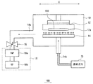
- FIG. 1 is a schematic view showing a plasma processing apparatus 200 according to an embodiment of the present invention.
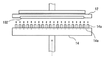
- FIG. 2 is an enlarged view of the periphery of the upper electrode and the lower electrode of the plasma processing apparatus 200.
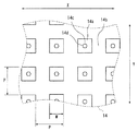
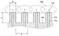
- 3 and 4 are a plan view and a cross-sectional view for explaining the structure of the lower electrode of the plasma processing apparatus 200 in detail.
- the plasma processing apparatus 200 has a parallel structure in which an upper electrode 12 and a lower electrode 14 are installed in a vacuum chamber 10 so as to face each other.
- the upper electrode 12 and the lower electrode 14 correspond to the “first electrode” and the “second electrode” in the present invention, respectively.
- the areas of the opposing surfaces of the upper electrode 12 and the lower electrode 14 are, for example, about 600 mm ⁇ about 600 mm.
- the upper electrode 12 is formed with a substrate holding portion 12a for holding the substrate 102 on which film formation or etching is performed on the side facing the lower electrode.
- the substrate 102 has a rectangular shape of about 400 mm ⁇ about 300 mm, for example.
- the upper electrode 12 is provided with a function capable of swinging in the X direction.
- the upper electrode 12 may include a heating / cooling mechanism (not shown) for maintaining the substrate 102 at a predetermined temperature.
- the lower electrode 14 has a columnar convex portion 14 a formed on the surface facing the upper electrode 12. This makes it possible to generate high-density plasma around the columnar protrusions 14a during film formation. Also, the height h from the tip of the columnar convex portion 14a shown in FIG. 4 to the bottom surface 14b between the columnar convex portions 14a is preferably about 5 mm to 10 mm.
- the columnar convex portion 14a is preferably a rectangular column having a constant width from the base portion toward the tip portion.
- the present invention is not limited to this, and may be a cylinder or a column shape formed so as to become narrower from the root portion toward the tip portion. As a result, the electric field can be more concentrated on the tip of the columnar convex portion 14a having a small width, so that higher density plasma can be generated.
- the columnar protrusions 14a are formed on the entire surface of the lower electrode 14 with a uniform density.
- the pitch P of the columnar protrusions 14a is preferably arranged so that the plasma generation regions 150 overlap between adjacent columnar protrusions 14a.
- the columnar convex portions 14a are preferably arranged at a pitch P of 5 mm or more and 20 mm or less in the X direction and the Y direction shown in FIG. Thereby, the density of the plasma generated between the upper electrode 12 and the lower electrode 14 can be made substantially uniform.
- the columnar convex portion 14a of the lower electrode 14 is provided with a gas supply port 14c for supplying gas to the plasma.
- the distal end portion 14d of the gas supply port 14c of the columnar convex portion 14a is formed to have a curved surface shape with a radius of about 0.5 mm or less.
- the vacuum chamber 10 has an exhaust port 10 a on the side, and the exhaust port 10 a is connected to the vacuum exhaust system 18 via the exhaust flow rate adjusting valve 16.
- the evacuation equipment 18 includes a turbo molecular pump (TMP) 18a and an oil rotary pump (RP) 18b.
- TMP turbo molecular pump
- RP oil rotary pump
- the gas supply port 14 c of the lower electrode 14 is connected to the source gas supply source 20.
- the electric field can be concentrated on the tip of the columnar protrusion 14 a of the lower electrode 14.
- high-density plasma can be generated on the columnar protrusions 14a of the lower electrode 14.
- the plasma processing apparatus 200 is used for film formation, the film formation rate can be improved, and when it is used for etching, the etching rate can be improved.
- the columnar convex portion 14a a quadrangular column
- the space between the columnar convex portions 14a is wider than when the columnar convex portion 14a needs an area for providing a tapered portion in a cone or a quadrangular pyramid shape.
- the gas can be smoothly exhausted from the exhaust port 10a of the vacuum chamber 10 which is maintained.
- the columnar convex portion 14a as a square column
- the columnar convex portion 14a can be formed simply by forming a groove having a rectangular cross section in the vertical and horizontal directions on the surface of the lower electrode 14, thereby facilitating processing.
- the pitch P of the columnar protrusions 14a is set so that the plasma generation region 150 centering on the tip of the columnar protrusion 14a overlaps the plasma generation region 150 centering on the adjacent columnar protrusion 14a.
- the plasma generation region 150 also extends to the region between the adjacent columnar protrusions 14a.
- the plasma generation region 150 can be expanded at a density that is nearly uniform over the entire surface of the lower electrode 14.
- nonuniformity of the film thickness and film quality over the entire surface of the lower electrode 14 can be reduced, and nonuniformity of the etching rate can be reduced.
- the upper electrode 12 and the substrate 102 are provided so as to be swingable in the X direction, and by swinging the upper electrode 12 and the substrate 102, the plasma in the tip region of the columnar convex portion 14a of the lower electrode 14 having a high plasma density can be obtained.
- the surface of 102 can be uniformly touched. Thereby, even if it is the structure which provided the discontinuous columnar convex part 14a, it can suppress that the film thickness and film quality of film-forming, and the etching speed become non-uniform
- the ratio P / W between the pitch P of the arrangement of the columnar convex portions 14a and the width W of the tip end portion of the columnar convex portions 14a is 1.3 or more.
- FIG. 5 shows the relationship of the discharge start voltage with respect to the ratio P / W between the pitch P of the columnar protrusions 14a formed on the lower electrode 14 and the width W of the tip.
- FIG. 5 shows the results obtained by simulation and experiment of the plasma discharge start voltage (Paschen minimum value) when the silicon thin film is formed in the plasma processing apparatus 200.
- the cross mark ( ⁇ ) indicates the simulation result
- the white diamond mark ( ⁇ ⁇ ⁇ ) indicates the experimental result.
- the procedure of the experiment conducted to obtain the experimental result shown in FIG. 5 is shown below.
- the inside of the vacuum chamber 10 is evacuated by the vacuum exhaust equipment 18 connected to the exhaust port 10 a of the vacuum chamber 10. Exhausted.
- the distance between the upper electrode 12 and the lower electrode 14 was 15 mm.
- the substrate 102 was held in a state heated to 230 ° C.
- hydrogen (H 2 ) and silane (SiH 4 ) as source gases are supplied between the upper electrode 12 and the lower electrode 14 from a gas supply port 14 c of the lower electrode 14 connected to the source gas supply source 20.
- hydrogen (H 2 ) was supplied at a flow rate of 100 sccm and silane (SiH 4 ) at a flow rate of 8 sccm so that the pressure in the vacuum chamber 10 was 1 Torr.
- high frequency power the same power was supplied under all conditions, and the frequency was set to 70 MHz.
- the source gas was decomposed by plasma to generate film formation species, and the film formation species deposited on the substrate 102, thereby forming a silicon thin film on the substrate 102.
- the raw material gas that was not used was exhausted from the exhaust port 10 a of the vacuum chamber 10.
- the discharge start voltage does not decrease, and when it becomes 1.3 or more, the discharge start voltage decreases rapidly. That is, by setting the ratio P / W between the tip width W and the pitch P to 1.3 or less, stable discharge can be performed at a lower voltage, and the gas decomposition reaction can be performed more efficiently. Thereby, the film-forming speed
- this embodiment is not restrictive, For example, while providing a gas supply port in the columnar convex part 14a, you may provide a gas suction port in the bottom part 14b pinched
- the present invention is not limited thereto, and the upper electrode 12 or the substrate 102 is changed. May be swung along the Y direction other than the X direction. By doing so, uniform film formation or etching can be performed in a local region.
- the swing width of the upper electrode 12 and the substrate 102 is preferably set to be equal to or greater than the pitch of the convex portions (about 7 mm).
- the plasma processing apparatus set so that the ratio P / W between the pitch P of the protrusions described above and the width W of the tip of the protrusions is 1.3 or more is also suitable as a solar cell manufacturing apparatus. Available to: Below, embodiment of the plasma processing apparatus 300 suitable when manufacturing a solar cell is shown.
- FIG. 6, which is a schematic diagram showing the plasma processing apparatus 300, and a schematic diagram showing the shower plate 40 of the upper electrode 13 of the plasma processing apparatus 300, for the plasma processing apparatus 300 in the present embodiment. Will be described.
- the vacuum chamber 10 is an example of the “processing chamber”, the “first electrode”, and the “second electrode” in the embodiment.
- the plasma processing apparatus 300 according to the second embodiment is different from the above-described embodiment in that a source gas is supplied from the upper electrode 13 and a voltage is applied to set the lower electrode 15 to a predetermined voltage.
- the vacuum chamber 10 has an exhaust port 10 a on the side, and the exhaust port 10 a is connected to the vacuum exhaust system 18 via the exhaust flow rate adjustment valve 16.
- the evacuation facility 18 includes a turbo molecular pump (TMP) 18a and an oil rotary pump (RP) 18b.
- the lower electrode 15 is formed with a substrate holding portion 15 a for holding the substrate 102 on the side facing the upper electrode 13.
- the lower electrode 15 includes a heating / cooling mechanism (not shown) for keeping the substrate 102 at a predetermined temperature.
- the surface which each of the upper electrode 13 and the lower electrode 15 opposes has an area of about 1500 mm x 1500 mm.
- the substrate 102 has an area of about 1400 mm ⁇ 1100 mm.
- the upper electrode 13 has a shower plate 40 arranged so as to face the substrate 102 held on the lower electrode 15.
- the shower plate 40 is provided with a plurality of convex portions 41... Arranged in a substantially lattice shape aligned in the XY direction.
- the tip of the projection 41 is formed to have a plane parallel to the XY plane, and a gas supply port 42 connected to the source gas supply source 20 is provided at the center.
- the gas supply ports 42 adjacent to each other in the X direction and the Y direction are arranged at equal intervals so as to have an interval of about 1 cm.
- the tip portions of the convex portions 41a to 41e are formed in a plane parallel to the XY plane. These planes are formed so as to be flush with the Z axis.
- the flush surface is not only that the planes of the tips of the convex portions 41a to 41e are completely located on the same XY plane, but the plane of the tips of the convex portions 41a to 41e is the Z axis. Including those having a height difference within about 1 mm in the direction.
- the flushness in the present invention includes a state that is substantially flush within the scope of achieving the intended purpose of the present invention.
- the widths H a to H e in the X direction of the tip portions of the convex portions 41 a to 41 e are formed so as to be smaller at the outer peripheral portion than at the central portion of the shower plate 40.
- the widths h a -h d in the X direction of the concave portions 43a-43d formed between the adjacent convex portions 41a-41e are larger at the outer peripheral portion than at the central portion of the shower plate 40. Formed as follows. That is, the shower plate 40 toward the outer peripheral portion from the central portion, the partial width H a ⁇ H e of the tip portion of the convex portion 41a ⁇ 41e is reduced, by increasing the width of the recess 43a ⁇ 43d, protrusions The intervals between the gas supply ports 42 provided at the center of the tip portions of 41a to 41e can be made constant.
- the widths h a to h d in the X direction of the recesses 43 a to 43 d are sequentially from the central part of the shower plate 40 toward the outer peripheral part as h a ⁇ h b ⁇ h c ⁇ h d.
- the depth to the bottom of the recesses 43a to 43d is formed so as to have the same depth in the Z direction over the central portion and the outer periphery of the shower plate 40.
- the shower plate 40 is formed so as to have the same relationship in the Y direction.
- this embodiment is not limited to the case where the plurality of convex portions 41... Are formed on the entire surface of the shower plate 40 illustrated in FIG. It is good also as what formed several convex part 41 ... only in the area
- the shower plate 40 may be a conductive member, and Cu, SUS, or the like may be used instead of Al used in the present embodiment.
- a film having a uniform film quality and film thickness can be formed over the entire surface of the substrate 102. This effect will be described in detail below.
- the shower plate 40 provided with the convex portions 41a to 41e in which the width of the tip portion with respect to the X / Y direction decreases from the central portion toward the outer peripheral portion is used.
- the electric field can be concentrated on the tips of the convex portions 41a to 41e, and the plasma generation region 200 made of high-density plasma can be generated near the tips.
- the convex part 41e located in the outer peripheral part compared with the convex part 41a located in the center part by reducing the width
- the concave portions 43a to 43d formed between the adjacent convex portions 41a to 41e provided in the shower plate 40 have a width in the X / Y direction at the outer peripheral portion as compared with the central portion of the shower plate 40. Is formed to be large. That is, in this embodiment, the space in which the gas formed by the substrate 102 and the respective recesses 43a to 43d flows is made wider on the outer peripheral portion B side than on the A side of the central portion of the substrate 102. Thereby, even when a large amount of source gas is supplied, the gas flow rate at the outer peripheral portion is prevented from increasing compared to the central portion of the substrate 102, and the gas flow velocity at the central portion and the outer peripheral portion of the substrate 102 is reduced. It can be made constant. Therefore, in the plasma processing apparatus 300 of the present embodiment, the film quality and film thickness can be suppressed from becoming nonuniform by making the gas flow rate substantially constant at the central portion and the outer peripheral portion of the substrate 102.
- the convex portions 41a to 41e provided on the shower plate 40 are formed in a substantially lattice shape, the gas can flow more easily from the central portion of the substrate 102 toward the outer peripheral portion. A film can be formed quickly.
- the distance between the centers (gas supply ports 42) of the adjacent convex portions 41a to 41e is about 1 cm so that the adjacent plasma generation regions 200 and 8 centering on the convex portions 41a to 41e overlap each other. .
- film formation seeds can be generated on the entire surface of the substrate 102 by the plasma generation regions 200, 200... Disposed on the entire surface of the upper electrode 13, so that the film quality and film thickness can be effectively reduced. Can be suppressed.
- the transparent conductive film 104, the photoelectric conversion units 106 and 108, and the back electrode 110 are sequentially stacked on the substrate 102.
- the substrate 102 is made of a light transmissive member such as glass, and is a single substrate of a solar cell. A plurality of photovoltaic elements are formed on the back side of the substrate 102 opposite to the light incident side.
- the transparent conductive film 104 (substrate side electrode) is formed on the substrate 102.
- ZnO is used as the transparent conductive film 104 because it has high light transmittance, low resistance, and plasticity, and is inexpensive.
- the photoelectric conversion units 106 and 108 are formed on the transparent conductive film 104, and the photoelectric conversion units 106 and 108 are made of an amorphous silicon semiconductor and a microcrystalline silicon semiconductor, respectively.
- the term “microcrystal” means not only a complete crystal state but also a state partially including an amorphous state.
- the back electrode 110 (back electrode) is made of a conductive member such as Ag and is formed on the photoelectric conversion units 106 and 108. Note that a layer made of a transparent conductive material may be interposed between the back electrode 110 and the photoelectric conversion unit 108.
- the photoelectric conversion units 106 and 108 in which an amorphous silicon semiconductor and a microcrystalline silicon semiconductor are sequentially stacked are used.
- a single layer or three or more layers of a microcrystalline or amorphous photoelectric conversion unit are used.
- a laminate may be used.
- an intermediate layer made of ZnO, SnO 2 , SiO 2 , or MgZnO may be provided between the first photovoltaic element and the second photovoltaic element to improve the optical characteristics.
- the transparent conductive film 104 is made of one or more kinds of laminated bodies selected from metal oxides of In 2 O 3 , SnO 2 , TiO 2 , and Zn 2 SnO 4 in addition to ZnO used in this embodiment. It may be configured.
- a 600 nm thick ZnO electrode 104 is formed on a 4 mm thick glass substrate 102 by sputtering.
- the photoelectric conversion units 106 and 13 are formed by the plasma processing apparatus of the above embodiment.
- the vacuum chamber 10 is evacuated by the evacuation equipment 18. The inside is evacuated.
- a source gas is supplied between the upper electrode 13 and the lower electrode 15 from a gas supply port 42 of the upper electrode 13 connected to the source gas supply source 20 (see FIG. 6). Thereafter, high frequency power is supplied to the upper electrode 13 to generate plasma around the convex portions 41a to 41e of the upper electrode 13. As a result, the source gas is decomposed by the plasma, and a film formation seed is generated. A predetermined film (not shown) is formed on the substrate 102 by depositing on the substrate 102 film-forming species generated by the source gas being decomposed by plasma.
- the photoelectric conversion unit 106 uses a plasma processing apparatus 300 to convert a p-type amorphous silicon semiconductor layer having a thickness of 10 nm with SiH 4 using a mixed gas of SiH 4 , CH 4 , H 2 and B 2 H 6 as a source gas.
- the i-type amorphous silicon semiconductor layer having a thickness of 300nm, a mixed gas as a source gas of H 2, SiH 4, thickness 20 nm n-type amorphous silicon of the mixed gas as a source gas of H 2 and PH 4
- a semiconductor layer is formed and sequentially stacked.
- the photoelectric conversion unit 108 converts a p-type microcrystalline silicon semiconductor layer having a film thickness of 10 nm into SiH 4 and H 2 using a mixed gas of SiH 4 , H 2, and B 2 H 6 as a source gas by the plasma processing apparatus 300.
- An i-type microcrystalline silicon semiconductor layer having a film thickness of 2000 nm is formed using a mixed gas of and a raw material gas
- an n-type microcrystalline silicon semiconductor layer having a film thickness of 20 nm is formed using a mixed gas of SiH 4 , H 2 and PH 4 as a raw material gas. Then, sequentially stack. Details of various conditions of the plasma processing apparatus are shown in Table 2 below.
- a 200 nm thick Ag electrode 110 is formed on the photoelectric conversion unit 108 by sputtering.
- the solar cell 120 is formed on the glass substrate 102.
- a filler 112 made of EVA (ethylene vinyl acetate) or the like and a back sheet 114 made of PET / Al foil / PET or the like are provided on the back electrode 110 of the solar cell 120.
- a solar cell module On the back electrode 110 of the solar cell 120, as shown in FIG. 9, a filler 112 made of EVA (ethylene vinyl acetate) or the like and a back sheet 114 made of PET / Al foil / PET or the like are provided. And a solar cell module.
- EVA ethylene vinyl acetate
- the present invention is not limited to this.
- at least a part of the photoelectric conversion units 106 and 108 may be formed by the plasma processing apparatus 300.
- ⁇ Action and effect> In the manufacturing method of the solar cell 120 of this embodiment, since it can suppress that film quality and a film thickness become non-uniform
- the following shower plate 50 can be applied to the solar cell manufacturing apparatus.
- the shower plate 50 will be described below.
- the shower plate 50 is provided with convex portions 51a to 51e formed concentrically.
- the tip portions of the convex portions 51a to 51e have a plane parallel to the XY plane and are formed to have a width of about 3 mm in the X / Y direction.
- a gas supply port 52 is provided at the center of the XY plane at the tip of the convex portions 51 a to 51 e, and this gas supply port 52 is connected to the source gas supply source 20.
- the tip portions of the convex portions 51a to 51e are formed in a plane parallel to the XY plane. These planes are formed so as to be flush with the Z axis.
- the flush surface is not only that the planes of the tips of the projections 51a to 51e are completely located on the same XY plane, but the planes of the tips of the projections 51a to 51e are Z-axis. Including those having a height difference within about 1 mm in the direction.
- the shower plate 50 uses an Al plate.
- the shower plate 50 may be a conductive member, and Cu, SUS, or the like may be used instead of Al used in the present embodiment.
- ⁇ Action and effect> According to the plasma processing apparatus 300 using the shower plate 50, a film having uniform film quality and film thickness can be formed over the entire surface of the substrate 102. This effect will be described in detail below.
- the shower plate 50 provided with the convex portions 51a to 51e is used.
- the electric field can be concentrated on the tips of the convex portions 51a to 51e, and the plasma generation region 200 made of high-density plasma can be generated near the tips. Since the source gas can be efficiently decomposed in the plasma generation region 200 to generate more film formation species, the film formation speed can be improved.
- the recesses 53a to 53d formed between the adjacent protrusions 51a to 51e provided on the shower plate 50 are formed so that the outer peripheral portion is closer to the Z from the tip than the center portion of the shower plate 50. It is formed so that the depth in the direction is deep. That is, in this embodiment, the space in which the gas formed by the substrate 102 and the respective recesses 53a to 53d flows is made wider on the B side of the outer peripheral portion than on the A side of the central portion of the substrate 102. Accordingly, even when a large amount of source gas is supplied, the gas flow rate at the outer peripheral portion is prevented from being higher than that at the central portion of the substrate 102, and the gas flow velocity at the central portion and the outer peripheral portion of the substrate 102 is constant. Can be. Therefore, in the plasma processing apparatus 300 of this embodiment, it is possible to prevent the film quality and film thickness from becoming nonuniform by making the gas flow rate substantially constant at the central portion and the outer peripheral portion of the substrate 102.
- the convex portions 51a to 51e provided on the shower plate 50 are formed concentrically. Thereby, the gas can easily flow better from the central portion of the substrate 102 toward the outer peripheral portion, and the film can be formed faster.
- the distance between the centers of the adjacent convex portions 51a to 51e is about 1 cm.
- the adjacent plasma generation regions 200 and 200 centering on the convex portions 51a to 51e overlap.
- the plasma generation regions 200, 200,... Disposed on the entire surface of the upper electrode 13 can generate film formation seeds on the entire surface of the substrate 102, thereby effectively suppressing nonuniform film quality and film thickness. Can do.
- Vacuum chamber 10a Exhaust port 12, 13 Upper electrode 12a, 15a Substrate holding part 14, 15 Lower electrode 14a, 41, 41a-41e, 51a-51e Convex part 14b Bottom part 14c, 42, 52 Gas supply port 14d Tip part 40, 50 shower plates 43, 43a to 43d, 53a to 53d Recess 16 Exhaust flow rate adjusting valve 18 Vacuum exhaust equipment 20
- Source gas supply source 102 Substrate 100, 300 Plasma processing apparatus 200 Plasma generation region
- the present invention can be used for a plasma processing apparatus.
Landscapes
- Physics & Mathematics (AREA)
- Engineering & Computer Science (AREA)
- Plasma & Fusion (AREA)
- Chemical & Material Sciences (AREA)
- Analytical Chemistry (AREA)
Abstract
【課題】プラズマ処理装置における電極間の電界をより強くする。 【解決手段】プラズマ処理装置100では、真空チャンバ10内に、基板102を保持することが可能な上部電極12と、上部電極12と対向するように配置された下部電極14と、を設ける。そして、下部電極14には上部電極12と対向する部分に上部電極12に向かって複数の柱状凸部14aが形成され、下部電極14に柱状凸部14aが、柱状凸部14aの配置のピッチPと先端部の幅Wとの比P/Wを1.3以上となる関係を満たすようにして配置される。
Description
本発明は、プラズマ処理装置に関する。
基板に対してプラズマによる成膜、エッチング等の処理を施すために、基板を保持することが可能な第1電極と、その第1電極と対向するように配置された第2電極とを備えた平行平板型のプラズマ処理装置が知られている(特許文献1~3参照)。
また、第2電極の第1電極に対向する面に複数の凹部と複数の凸部とを形成し、凹部又は凸部の一方にガス供給口を形成し、他方にガス排気口を形成したプラズマ処理装置の構成も開示されている(特許文献4参照)。
このようなプラズマ処理装置では、プラズマによる処理能力を高めるためにプラズマの密度をより高くすることが重要である。プラズマの密度を高めるためには、第1電極と第2電極との間の電界を大きくする必要がある。
本発明は、電極間の電界をより強めたプラズマ処理装置を提供することを目的とする。
本発明の1つの態様は、基板を保持することが可能な第1電極と、第1電極と対向するように配置され、第1電極と対向する部分に第1電極に向かって複数の柱状凸部が形成された第2電極と、を備え、柱状凸部の配置のピッチPと、柱状凸部の先端部の幅Wと、の比P/Wが1.3以上である、プラズマ処理装置である。
本発明によれば、電極間の電界を強めたプラズマ処理装置を提供することができる。
図1は、本発明の実施形態におけるプラズマ処理装置200を示した概略図である。図2は、プラズマ処理装置200の上部電極及び下部電極の周辺の拡大図である。図3及び図4は、プラズマ処理装置200の下部電極の構造を詳細に説明するための平面図及び断面図である。
プラズマ処理装置200は、図1に示すように、真空チャンバ10内に、上部電極12と下部電極14とが互いに対向するように設置された平行型構造を有する。また、上部電極12及び下部電極14は、それぞれ本発明における「第1電極」及び「第2電極」に相当する。上部電極12及び下部電極14の対向する面の面積は、例えば、約600mm×約600mmとされる。また、上部電極12には、下部電極14と対向する側に成膜又はエッチングを施す基板102を保持するための基板保持部12aが形成されている。基板102は、例えば、約400mm×約300mmの矩形形状を有している。また、上部電極12は、X方向に揺動可能な機能が設けられている。また、上部電極12は、基板102を所定の温度に保持するための加熱冷却機構部(図示せず)を備えてもよい。
下部電極14は、図2に示すように、上部電極12と対向する面に柱状凸部14aが形成されている。これにより、成膜時に柱状凸部14aを中心として高密度なプラズマを発生させることが可能となる。また、図4に示す柱状凸部14aの先端部から柱状凸部14aの間の底面14bまでの高さhは、5mm~10mm程度とすることが好適である。
また、図3及び図4に示すように、柱状凸部14aは根元部から先端部に向かって幅が一定の四角柱とすることが好適である。ただし、これに限定されるものではなく、円柱としてもよいし、根元部から先端部に向かって細くなるように形成された柱形状としてもよい。これにより、柱状凸部14aの幅の小さい先端部に電界をより集中させることが可能となるので、より高密度なプラズマを発生させることが可能となる。
また、柱状凸部14aは、下部電極14の全面に均一な密度で形成することが好適である。このとき、柱状凸部14aの配置のピッチPは、図4に示すように、隣接する柱状凸部14a間で、プラズマ発生領域150がオーバラップするように配置することが好適である。例えば、柱状凸部14aは、図3に示すX方向及びY方向にそれぞれ5mm以上20mm以下のピッチPで配置することが好適である。これにより、上部電極12と下部電極14との間に発生するプラズマの密度を略均一にすることができる。
また、下部電極14の柱状凸部14aには、プラズマにガスを供給するためのガス供給口14cが設けられている。また、柱状凸部14aのガス供給口14cの先端部14dは、半径が約0.5mm以下の曲面形状を有するように形成されている。これにより、ガス供給口14cから供給されるガスを柱状凸部14aの先端付近で滞留させることが可能となるので、プラズマ発生領域150における原料ガスの滞留時間を長くすることが可能となる。
このような構成とすることにより、例えば、プラズマ処理装置200を成膜に用いた場合にはより多くの成膜種を生成することが可能となり、成膜速度をより大きくすることが可能となる。
また、図1に示すように、真空チャンバ10は、側方に排気口10aを有するとともに、その排気口10aは、排気流量調整バルブ16を介して真空排気設備18に接続されている。この真空排気設備18は、ターボ分子ポンプ(TMP)18a及び油回転ポンプ(RP)18bによって構成されている。また、下部電極14のガス供給口14cは、原料ガス供給源20に接続されている。
下部電極14において上部電極12と対向する面に複数の柱状凸部14aを設けることによって、下部電極14の柱状凸部14aの先端部に電界を集中させることができる。これによって、下部電極14の柱状凸部14aに高密度なプラズマを発生させることができる。その結果、プラズマ化されるガスの分解効率を向上させることができる。プラズマ処理装置200を成膜に用いる場合には成膜速度を向上させることができ、エッチングに用いる場合にはエッチング速度を向上させることができる。
また、柱状凸部14aを四角柱とすることによって、柱状凸部14aが円錐又は四角錐形状におけるテーパ部を設ける分の面積が必要になる場合に比べて柱状凸部14aの間の空間が広く保たれ真空チャンバ10の排気口10aからのガスの排気をスムーズに行うことが可能となる。さらに、柱状凸部14aを四角柱とすることによって、下部電極14の表面に縦及び横に矩形断面形状の溝を形成するだけで柱状凸部14aを形成することができ、加工が容易になる利点もある。
また、柱状凸部14aの先端部を中心とするプラズマ発生領域150が隣接する柱状凸部14aを中心とするプラズマ発生領域150とオーバラップするように、柱状凸部14aのピッチPを設定することによって、隣接する柱状凸部14a間の領域にもプラズマ発生領域150が広がる。これにより、プラズマ発生領域150を下部電極14の全面により均一に近い密度で広げることができる。その結果、下部電極14の全面での膜の膜厚や膜質の不均一性を低減したり、エッチングの速度の不均一性を低減したりすることができる。
また、上部電極12及び基板102をX方向に揺動可能に設け、上部電極12及び基板102を揺動させることによって、プラズマ密度の高い下部電極14の柱状凸部14aの先端領域のプラズマを基板102の表面に均一に触れさせることができる。これによって、不連続な柱状凸部14aを設けた構成であっても成膜の膜厚及び膜質やエッチングの速度が不均一になることを抑制することができる。
また、柱状凸部14aの配置のピッチPと柱状凸部14aの先端部の幅Wとの比P/Wが1.3以上となるように設定することが好適である。このような比P/Wの関係とすることによって、プラズマ処理装置200で発生されるプラズマの密度をより高くすることができる。
図5は、下部電極14に形成する柱状凸部14aの配置のピッチPと先端部の幅Wとの比P/Wに対する放電開始電圧の関係を示す。図5は、プラズマ処理装置200においてシリコン薄膜を形成する際のプラズマの放電開始電圧(パッシェンミニマム値)をシミュレーション及び実験で得た結果を示す。図5において、クロスマーク(×)がシミュレーション結果を示し、白抜き菱形マーク(◇)が実験結果を示す。
以下、図5に示す実験結果を得るために行った実験の手順を示す。図1に示すように、プラズマ処理装置200の上部電極12の基板保持部12aに基板102を固定した後、真空チャンバ10の排気口10aに接続された真空排気設備18により真空チャンバ10内を真空排気した。上部電極12と下部電極14との距離は15mmとした。また、基板102は230℃に加熱した状態で保持した。
次に、上部電極12と下部電極14との間に、原料ガス供給源20に接続された下部電極14のガス供給口14cから原料ガスである水素(H2)とシラン(SiH4)を供給した。ここでは、水素(H2)を100sccm及びシラン(SiH4)を8sccmの流量で真空チャンバ10内の圧力が1Torrとなるように供給した。そして、下部電極14に高周波電力を供給することにより、下部電極14の柱状凸部14aを中心としてプラズマを発生させた。ここで、高周波電力としては総ての条件において同一の電力を供給し、周波数は70MHzとした。原料ガスがプラズマにより分解されて成膜種が生成され、成膜種が基板102上に堆積することによって、基板102上にシリコン薄膜が形成された。利用されなかった原料ガスは、真空チャンバ10の排気口10aから排気した。
ここで、下部電極14の柱状凸部14aの先端幅WとピッチPとの組み合わせは表1に示すものとした。表1に示した先端幅WとピッチPとの組み合わせについて、それぞれ上記の成膜条件下において放電開始電圧(パッシェンミニマム値)を計算及び測定した。放電開始電圧が低いほどより低電圧で安定放電が可能であり、ガスの分解反応がより効率良く行われていることを示している。

図5に示すように、先端幅WとピッチPとの比P/Wが1.3未満では放電開始電圧の低下はみられず、1.3以上となると急激に放電開始電圧が低下する。すなわち、先端幅WとピッチPとの比P/Wを1.3以下とすることによって、より低電圧で安定放電が可能となり、ガスの分解反応をより効率良く行うことができる。これにより、プラズマ処理装置200による成膜速度やエッチング速度の向上を図ることができる。
なお、本実施形態は、制限的なものではなく、例えば、柱状凸部14aにガス供給口を設けるとともに、柱状凸部14aに挟まれた底部14bにガス吸引口を設けてもよい。また、下部電極14の柱状凸部14aにガス吸引口を設けるとともに、柱状凸部14aに挟まれた底部14bにガス供給口を設けてもよい。このようにすることにより、大面積において均一な成膜又はエッチングが可能となる。
また、上記実施形態では、上部電極12をX方向に揺動させることによって基板102との相対的な位置を変化させる例を示したが、本発明はこれに限らず、上部電極12又は基板102をX方向以外のたとえばY方向に沿って揺動してもよい。このようにすることにより、局所的な領域において、均一な成膜又はエッチングが可能となる。なお、上部電極12及び基板102の揺動幅は、凸部のピッチ(約7mm)以上に設定するのが望ましい。
上記に記載した凸部の配置のピッチPと凸部の先端部の幅Wとの比P/Wが1.3以上となるように設定したプラズマ処理装置は、太陽電池の製造装置としても好適に利用できる。以下に、太陽電池を製造する際に好適なプラズマ処理装置300の実施形態を示す。
〈プラズマ処理装置の構成〉
以下に、本実施形態におけるプラズマ処理装置300について、プラズマ処理装置300を示した概略図である図6、およびこのプラズマ処理装置300の上部電極13のシャワープレート40を示した概略図である図7を用いて説明する。
以下に、本実施形態におけるプラズマ処理装置300について、プラズマ処理装置300を示した概略図である図6、およびこのプラズマ処理装置300の上部電極13のシャワープレート40を示した概略図である図7を用いて説明する。
図6に示すように、真空チャンバ10内には実施形態の「処理室」、「第1電極」および「第2電極」の一例である。なお、第2実施形態によるプラズマ処理装置300は、上部電極13より原料ガスを供給するとともに電圧を印加し、下部電極15を所定の電圧とする点で上記実施形態と異なる。
また、真空チャンバ10は、側方に排気口10aを有するとともに、その排気口10aは、排気流量調整バルブ16を介して真空排気設備18に接続される。本実施形態では、真空排気設備18は、ターボ分子ポンプ(TMP)18aおよび油回転ポンプ(RP)18bによって構成される。
下部電極15は、上部電極13と対向する側に基板102を保持するための基板保持部15aが形成される。この下部電極15は、基板102を所定の温度に保持するための図示しない加熱冷却機構部を含む。上部電極13および下部電極15のそれぞれが対向する表面は、約1500mm×1500mmの面積を有する。また、基板102は、約1400mm×1100mmの面積を有する。
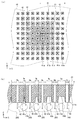
また、上部電極13は、下部電極15上に保持された基板102に対向するように配置されたシャワープレート40を有する。シャワープレート40には、図7(a)に示した上面図のように、X-Y方向に整列する略格子状に配置された複数の凸部41・・・が設けられる。この凸部41の先端部は、X-Y面と平行な面を有するように形成され、中心には原料ガス供給源20に接続されたガス供給口42が設けられる。なお、X方向およびY方向に隣接するガス供給口42は、1cm程度の間隔となるように等間隔に配置される。
また、図7(a)のA-B断面を示した図7(b)のように、凸部41a~41eの先端部は、X-Y面と平行な面が形成され、いずれの先端部の平面はZ軸において面一となるように形成されている。なお、ここでの面一とは凸部41a~41eの先端部の平面が完全に同一のX-Y平面上に位置するもののみでなく、凸部41a~41eの先端部の平面がZ軸方向に約1mm以内の高低差を有するものをも含む。つまり、本発明における面一とは、本発明の所期の目的を達成する範囲で実質的に面一である状態を含む。
凸部41a~41eの先端部のX方向における幅Ha~Heは、シャワープレート40の中央部に比べて外周部に位置するものの方が小さくなるように形成される。本実施形態では、凸部41a~41eの先端部のX方向における幅Ha~Heは、Ha>Hb>Hc>Hd>Heのように、シャワープレート40の中央部から外周部に向かって順々に小さくなるものとしたが、例えばHa=Hb>Hc=Hd>Heのように段階的に小さくなるようにしても良い。
一方、隣接する凸部41a~41eの間に形成された凹部43a~43dのX方向における幅ha~hdは、シャワープレート40の中央部に比べて外周部に位置するものの方が大きくなるように形成される。つまり、シャワープレート40は中央部から外周部に向かって、凸部41a~41eの先端部の幅Ha~Heが小さくなった分、凹部43a~43dの幅を大きくすることにより、凸部41a~41eの先端部の中央部に設けられた各々のガス供給口42の間隔を一定とすることができる。本実施形態では、凹部43a~43dのX方向における幅ha~hdは、ha<hb<hc<hdのように、シャワープレート40の中央部から外周部に向かって順々に大きくなるものとしたが、例えばha=hb<hc=hdのように段階的に小さくなるようにしても良い。
なお、凹部43a~43dの底部までの深さは、シャワープレート40の中央部および外周部に亘って、Z方向に同じ深さを有するように形成される。
上記の記載では、X方向における凸部41a~41eおよび凹部43a~43dの幅の関係を説明したが、Y方向においても同様の関係となるようにシャワープレート40が形成される。
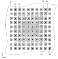
なお、本実施形態は図7(a)に記載したシャワープレート40の全面に複数の凸部41・・・を形成したものに限らず、図8に記載したようにシャワープレート40の外周部の領域にだけ複数の凸部41・・・を形成したものとしても良い。
シャワープレート40としては、Al板を用いる。このシャワープレート40は導電性部材であればよく、本実施形態で用いたAlの代わりに、Cu,SUSなどを用いても良い。
〈作用および効果〉
本実施形態に係るプラズマ処理装置300によれば、基板102全面に渡って均一な膜質と膜厚を有する膜を成膜することができる。このような効果について、以下に詳説する。
〈作用および効果〉
本実施形態に係るプラズマ処理装置300によれば、基板102全面に渡って均一な膜質と膜厚を有する膜を成膜することができる。このような効果について、以下に詳説する。
(1)本実施形態に係るプラズマ処理装置300では、中央部から外周部に向かってX/Y方向に対する先端部の幅が小さくなった凸部41a~41eが設けられたシャワープレート40を用いる。これにより、凸部41a~41eの先端部に電界を集中させることが可能となり、先端部付近に高密度なプラズマからなるプラズマ発生領域200を発生させることができる。さらには、シャワープレート40の中央部に比べて外周部に位置する凸部41の先端部の幅を小さくすることにより、中央部に位置する凸部41aに比べて外周部に位置する凸部41eの方がより良く電界を集中させることが可能となり、より活性なプラズマ発生領域200を発生させることができる。これにより、中央部に比べて原料ガス濃度が希釈され易い外周部においても、このプラズマ発生領域200で効率良く原料ガスを分解し、より多くの活性種を生成することが可能となるので、外周部における成膜速度を向上させることができる。
(2)シャワープレート40に設けられた隣接する凸部41a~41eの間に形成された凹部43a~43dを、シャワープレート40の中央部に比べ、外周部の方がX/Y方向への幅が大きくなるように形成する。つまり、本実施形態では基板102とそれぞれの凹部43a~43dで形成されるガスが流れる空間を、基板102の中央部のA側に比べて外周部B側の方が広くなるようにする。これにより、原料ガスを大量供給した場合であっても、基板102中央部に比べて外周部でのガスの流速が速くなることを抑制し、基板102の中央部と外周部におけるガスの流速が一定となるようにすることができる。したがって、本実施形態のプラズマ処理装置300では、基板102中央部と外周部において、ガスの流速をほぼ一定にすることにより、膜質および膜厚が不均一になることを抑制することができる。
(3)シャワープレート40に設けられた凸部41a~41eを、略格子状に形成しているので、基板102の中央部から外周部に向かってより良くガスが流れやすくすることができ、より早く成膜することができる。
(4)隣接する凸部41a~41eの中心(ガス供給口42)間は、凸部41a~41eを中心とする隣接し合うプラズマ発生領域200、8とがオーバラップするように1cm程度とする。これにより、上部電極13の全面に配置されたプラズマ発生領域200、200…により、基板102の全面で成膜種を生成することができるので、膜質および膜厚が不均一になるのを有効に抑制することができる。
〈太陽電池の構成〉
次に、プラズマ処理装置300を用いて太陽電池120を製造する方法について説明する。
次に、プラズマ処理装置300を用いて太陽電池120を製造する方法について説明する。
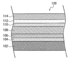
本実施形態で製造される太陽電池120は、図9に示すように、基板102上に透明導電膜104と光電変換ユニット106および108と裏面電極110とを順次積層される。
基板102は、ガラス等の光透過性の部材により構成され、太陽電池の単一基板である。この基板102の光入射側と反対の裏面側に複数の光起電力素子が形成される。
透明導電膜104(基板側電極)は、基板102上に形成される。透明導電膜104として、本実施形態では高い光透過性、低抵抗性、可塑性を有し、低価格であるため好適なZnOを用いる。
光電変換ユニット106および108は、透明導電膜104上に形成され、光電変換ユニット106および108は、それぞれ非晶質シリコン半導体および微結晶シリコン半導体により構成される。なお、本明細書において、「微結晶」の用語は、完全な結晶状態のみならず、部分的に非結晶状態を含む状態をも意味するものとする。
裏面電極110(裏面側電極)は、Ag等の導電性部材により構成され、光電変換ユニット106および108上に形成される。なお、裏面電極110と光電変換ユニット108の間に透明導電材料からなる層を介在させても良い。
上記の実施形態では、非晶質シリコン半導体と微結晶シリコン半導体とが順次積層された光電変換ユニット106および108を用いたが、微結晶又は非晶質光電変換ユニットの単層又は3層以上の積層体を用いても良い。また、第1光起電力素子と第2光起電力素子の間にZnO,SnO2,SiO2,MgZnOからなる中間層を設け、光学的特性を向上させた構造としても良い。さらに、透明導電膜104は、本実施形態で用いたZnOの他、In2O3,SnO2,TiO2,Zn2SnO4の金属酸化物より選択された一種類あるいは複数種類の積層体により構成しても良い。
〈太陽電池の製造方法〉
以下に、プラズマ処理装置300を用いた上述の太陽電池120の製造方法について説明する。
以下に、プラズマ処理装置300を用いた上述の太陽電池120の製造方法について説明する。
初めに、4mm厚のガラス基板102上に、スパッタにより600nm厚のZnO電極104を形成する。
次に、上記実施形態のプラズマ処理装置により、光電変換ユニット106および13を形成する。
詳述すると図6に示すように、プラズマ処理装置300の下部電極15の上部電極13と対向する面に形成された基板保持部15aに基板102を固定した後、真空排気設備18により真空チャンバ10内を真空排気する。
そして、上部電極13と下部電極15との間に、図7に示すように、原料ガス供給源20(図6参照)に接続された上部電極13のガス供給口42から原料ガスを供給する。この後、上部電極13に高周波電力を供給することにより、上部電極13の凸部41a~41eを中心としてプラズマを発生させる。これにより、原料ガスがプラズマにより分解されて成膜種が生成される。原料ガスがプラズマにより分解されて生成された成膜種が基板102上に堆積することによって、基板102上に所定の膜(図示せず)が形成される。
光電変換ユニット106は、プラズマ処理装置300により、SiH4、CH4、H2およびB2H6との混合ガスを原料ガスとして膜厚10nmのp型非晶質シリコン半導体層を、SiH4とH2との混合ガスを原料ガスとして膜厚300nmのi型非晶質シリコン半導体層を、SiH4、H2およびPH4との混合ガスを原料ガスとして膜厚20nmのn型非晶質シリコン半導体層を形成し順次積層する。又、光電変換ユニット108は、プラズマ処理装置300により、SiH4、H2およびB2H6との混合ガスを原料ガスとして膜厚10nmのp型微結晶シリコン半導体層を、SiH4とH2との混合ガスを原料ガスとして膜厚2000nmのi型微結晶シリコン半導体層を、SiH4、H2およびPH4との混合ガスを原料ガスとして膜厚20nmのn型微結晶シリコン半導体層を形成し順次積層する。以下にプラズマ処理装置の諸条件の詳細を表2に示す。
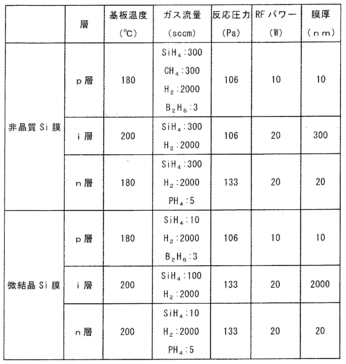
次に、200nm厚のAg電極110を、光電変換ユニット108上にスパッタにより形成する。
以上により、ガラス基板102上に太陽電池120を形成する。そして、この太陽電池120の裏面電極110上には、図9で示すようにEVA(エチレン・ビニル・アセテート)等からなる充填剤112、およびPET/Al箔/PET等からなるバックシート114を設け、太陽電池モジュールとする。
なお、上記実施形態では、光電変換ユニット106および108の全てをプラズマ処理装置300によって形成する例を示したが、本発明はこれに限らない。本発明では、光電変換ユニット106および108の少なくとも一部をプラズマ処理装置300によって形成すればよい。
〈作用および効果〉
本実施形態の太陽電池120の製造方法では、成膜速度を大きくしても膜質および膜厚が不均一になることを抑制できるため、所望の良好な膜を形成することができる。この結果、膜質および膜厚の不均一に起因する変換効率の低下を防止することができ、より大きな電力を取り出すことができる。即ち、本実施形態の太陽電池の製造方法では、成膜速度の向上と太陽電池の変換効率の低下防止を両立することができる。
〈作用および効果〉
本実施形態の太陽電池120の製造方法では、成膜速度を大きくしても膜質および膜厚が不均一になることを抑制できるため、所望の良好な膜を形成することができる。この結果、膜質および膜厚の不均一に起因する変換効率の低下を防止することができ、より大きな電力を取り出すことができる。即ち、本実施形態の太陽電池の製造方法では、成膜速度の向上と太陽電池の変換効率の低下防止を両立することができる。
さらに、シャワープレート40の代わりに、下記のシャワープレート50を太陽電池製造装置に適用することもできる。シャワープレート50について、以下に説明する。
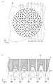
シャワープレート50には、図10(a)に示した上面図のように、同心円状に形成された凸部51a~51eが設けられる。この凸部51a~51eの先端部は、X-Y面と平行な面を有し、X/Y方向にいずれも3mm程度の幅となるように形成される。凸部51a~51eの先端部のX-Y平面の中心には、ガス供給口52を設けられ、このガス供給口52は原料ガス供給源20に接続される。
また、図10(a)のA-B断面を示した図10(b)のように、凸部51a~51eの先端部は、X-Y面と平行な面が形成され、いずれの先端部の平面はZ軸において面一となるように形成されている。なお、ここでの面一とは凸部51a~51eの先端部の平面が完全に同一のX-Y平面上に位置するもののみでなく、凸部51a~51eの先端部の平面がZ軸方向に約1mm以内の高低差を有するものをも含む。
さらに、隣接する凸部51a~51eの間に形成された凹部53a~53dの底部までの深さは、シャワープレート50の中央部に比べ、外周部の方が先端部からのZ方向に深くなるように形成される。本実施形態では、凹部53a~53dの底部までの深さは、53a=53b<53c<53dのように段階的に基板102中央部のA側から外周部のB側に向かって深くなるように形成したが、例えば53a<53b<53c<53d<45eのように基板102中央部から外周部に向かって順々に先端部から底部までの深さが深くなるように形成しても良い。
シャワープレート50は、Al板を用いる。このシャワープレート50は導電性部材であればよく、本実施形態で用いたAlの代わりに、Cu,SUSなどを用いても良い。
〈作用および効果〉
シャワープレート50を用いたプラズマ処理装置300によれば、基板102全面に渡って均一な膜質と膜厚を有する膜を成膜することができる。このような効果について、以下に詳説する。
〈作用および効果〉
シャワープレート50を用いたプラズマ処理装置300によれば、基板102全面に渡って均一な膜質と膜厚を有する膜を成膜することができる。このような効果について、以下に詳説する。
(1)本実施形態に係るプラズマ処理装置300では、凸部51a~51eが設けられたシャワープレート50を用いる。これにより、凸部51a~51eの先端部に電界を集中させることが可能となり、先端部付近に高密度なプラズマからなるプラズマ発生領域200を発生させることができる。このプラズマ発生領域200で効率良く原料ガスを分解してより多くの成膜種を生成することが可能となるので、成膜速度を向上させることができる。
(2)さらに、シャワープレート50に設けられた隣接する凸部51a~51eの間に形成された凹部53a~53dを、シャワープレート50の中央部に比べ、外周部の方が先端部からのZ方向への深さが深くなるように形成される。つまり、本実施形態では基板102とそれぞれの凹部53a~53dで形成されるガスが流れる空間を、基板102の中央部のA側に比べて外周部のB側の方が広くなるようにする。これにより、原料ガスを大量供給した場合であっても、基板102中央部に比べて外周部でのガスの流速が速くなることを抑制し、基板102の中央部と外周部におけるガス流速が一定となるようにすることができる。したがって、本実施形態のプラズマ処理装置300では、基板102中央部と外周部において、ガス流速をほぼ一定にすることにより、膜質および膜厚が不均一になることを抑制することができる。
(3)また、シャワープレート50に設けられた凸部51a~51eは、同心円状に形成される。これにより、基板102の中央部から外周部に向かってより良くガスが流れやすくすることができ、より早く成膜することができる。
(4)さらに、隣接する凸部51a~51eの中心間は、1cm程度とする。これにより、凸部51a~51eを中心とする隣接し合うプラズマ発生領域200、200とがオーバラップする。上部電極13の全面に配置されたプラズマ発生領域200、200…により、基板102の全面で成膜種を生成することができるので、膜質および膜厚が不均一になるのを有効に抑制することができる。
10 真空チャンバ
10a 排気口
12、13 上部電極
12a、15a 基板保持部
14、15 下部電極
14a、41、41a~41e、51a~51e 凸部
14b 底部
14c、42、52 ガス供給口
14d 先端部
40、50 シャワープレート
43、43a~43d、53a~53d 凹部
16 排気流量調整バルブ
18 真空排気設備
20 原料ガス供給源
102 基板
100、300 プラズマ処理装置
200 プラズマ発生領域
10a 排気口
12、13 上部電極
12a、15a 基板保持部
14、15 下部電極
14a、41、41a~41e、51a~51e 凸部
14b 底部
14c、42、52 ガス供給口
14d 先端部
40、50 シャワープレート
43、43a~43d、53a~53d 凹部
16 排気流量調整バルブ
18 真空排気設備
20 原料ガス供給源
102 基板
100、300 プラズマ処理装置
200 プラズマ発生領域
本発明は、プラズマ処理装置に利用可能である。
Claims (3)
- 基板を保持することが可能な第1電極と、
前記第1電極と対向するように配置され、前記第1電極と対向する部分に前記第1電極
に向かって複数の柱状凸部が形成された第2電極と、を備え、
前記柱状凸部の配置のピッチPと、前記柱状凸部の先端部の幅Wと、の比P/Wが1.3以上であることを特徴とするプラズマ処理装置。 - 請求項1に記載のプラズマ処理装置であって、
前記柱状凸部は、四角柱であることを特徴とするプラズマ処理装置。 - 請求項1又は2に記載のプラズマ処理装置であって、
前記柱状凸部には、先端部からガスを供給するためのガス供給口が形成されていること
を特徴とするプラズマ処理装置。
Applications Claiming Priority (6)
| Application Number | Priority Date | Filing Date | Title |
|---|---|---|---|
| JP2010-043154 | 2010-02-26 | ||
| JP2010043154A JP2011181625A (ja) | 2010-02-26 | 2010-02-26 | プラズマ処理装置 |
| JP2010074867A JP2011210797A (ja) | 2010-03-29 | 2010-03-29 | プラズマ処理装置およびそれよって製造される太陽電池の製造方法 |
| JP2010-074867 | 2010-03-29 | ||
| JP2010-092336 | 2010-04-13 | ||
| JP2010092336A JP2011222863A (ja) | 2010-04-13 | 2010-04-13 | プラズマ処理装置およびそれよって製造される太陽電池の製造方法 |
Publications (1)
| Publication Number | Publication Date |
|---|---|
| WO2011105158A1 true WO2011105158A1 (ja) | 2011-09-01 |
Family
ID=44506579
Family Applications (1)
| Application Number | Title | Priority Date | Filing Date |
|---|---|---|---|
| PCT/JP2011/051601 Ceased WO2011105158A1 (ja) | 2010-02-26 | 2011-01-27 | プラズマ処理装置 |
Country Status (1)
| Country | Link |
|---|---|
| WO (1) | WO2011105158A1 (ja) |
Cited By (1)
| Publication number | Priority date | Publication date | Assignee | Title |
|---|---|---|---|---|
| JP2019220589A (ja) * | 2018-06-20 | 2019-12-26 | 株式会社ニューフレアテクノロジー | 気相成長装置 |
Citations (2)
| Publication number | Priority date | Publication date | Assignee | Title |
|---|---|---|---|---|
| JPH09129563A (ja) * | 1995-11-02 | 1997-05-16 | Ulvac Japan Ltd | シャワープレート |
| JP2009253102A (ja) * | 2008-04-08 | 2009-10-29 | Shimadzu Corp | プラズマcvd用のカソード電極、およびプラズマcvd装置 |
-
2011
- 2011-01-27 WO PCT/JP2011/051601 patent/WO2011105158A1/ja not_active Ceased
Patent Citations (2)
| Publication number | Priority date | Publication date | Assignee | Title |
|---|---|---|---|---|
| JPH09129563A (ja) * | 1995-11-02 | 1997-05-16 | Ulvac Japan Ltd | シャワープレート |
| JP2009253102A (ja) * | 2008-04-08 | 2009-10-29 | Shimadzu Corp | プラズマcvd用のカソード電極、およびプラズマcvd装置 |
Cited By (2)
| Publication number | Priority date | Publication date | Assignee | Title |
|---|---|---|---|---|
| JP2019220589A (ja) * | 2018-06-20 | 2019-12-26 | 株式会社ニューフレアテクノロジー | 気相成長装置 |
| JP7164332B2 (ja) | 2018-06-20 | 2022-11-01 | 株式会社ニューフレアテクノロジー | 気相成長装置 |
Similar Documents
| Publication | Publication Date | Title |
|---|---|---|
| JP5069791B2 (ja) | 薄膜光電変換装置とその製造方法 | |
| JP4940290B2 (ja) | 光電変換装置及びその製造方法 | |
| JP4902779B2 (ja) | 光電変換装置及びその製造方法 | |
| CN102712999B (zh) | 涂覆基材的方法 | |
| JP6125594B2 (ja) | 光電変換装置の作製方法 | |
| JP2006310503A (ja) | 積層型光起電力装置 | |
| WO2009055388A1 (en) | Nip-nip thin-film photovoltaic structure | |
| WO2010074283A1 (ja) | パッシベーション膜形成用成膜装置及び成膜方法、並びに太陽電池素子の製造方法 | |
| JP4532008B2 (ja) | 反射防止膜の成膜方法 | |
| EP2549544A1 (en) | Solar cell and method for manufacturing same | |
| WO2010113709A1 (ja) | プラズマ処理装置およびそれによって製造される太陽電池の製造方法 | |
| JP2011210797A (ja) | プラズマ処理装置およびそれよって製造される太陽電池の製造方法 | |
| JP2007266094A (ja) | プラズマcvd装置及びプラズマcvdによる半導体薄膜の成膜方法 | |
| US8158531B2 (en) | Method of manufacturing solar cell and plasma treatment apparatus | |
| WO2010110158A1 (ja) | プラズマ処理装置およびそれによって製造される光起電力素子の製造方法 | |
| JP2011222863A (ja) | プラズマ処理装置およびそれよって製造される太陽電池の製造方法 | |
| JP2012119341A (ja) | プラズマ処理装置及び光起電力素子の製造方法 | |
| JP4215608B2 (ja) | 光起電力装置 | |
| JP2012119342A (ja) | プラズマ処理装置及び光起電力素子の製造方法 | |
| JP4642126B2 (ja) | 積層型光起電力素子および積層型光起電力素子の製造方法 | |
| JP5373045B2 (ja) | 光電変換装置 | |
| JP2013536991A (ja) | a−Si単接合および多接合薄膜シリコン太陽電池のための向上したa−Si:H吸収体層 | |
| JP5525298B2 (ja) | 導電性窒化シリコン膜の製造方法 | |
| JP2007184505A (ja) | シリコン系薄膜光電変換装置の製造方法 | |
| JP2010258103A (ja) | 光電変換デバイスの製造方法および製造装置 |
Legal Events
| Date | Code | Title | Description |
|---|---|---|---|
| 121 | Ep: the epo has been informed by wipo that ep was designated in this application |
Ref document number: 11747122 Country of ref document: EP Kind code of ref document: A1 |
|
| NENP | Non-entry into the national phase |
Ref country code: DE |
|
| 122 | Ep: pct application non-entry in european phase |
Ref document number: 11747122 Country of ref document: EP Kind code of ref document: A1 |