WO2011104932A1 - 高周波用誘電体付着材 - Google Patents
高周波用誘電体付着材 Download PDFInfo
- Publication number
- WO2011104932A1 WO2011104932A1 PCT/JP2010/068888 JP2010068888W WO2011104932A1 WO 2011104932 A1 WO2011104932 A1 WO 2011104932A1 JP 2010068888 W JP2010068888 W JP 2010068888W WO 2011104932 A1 WO2011104932 A1 WO 2011104932A1
- Authority
- WO
- WIPO (PCT)
- Prior art keywords
- dielectric
- layer
- sheet layer
- frequency
- adhesive layer
- Prior art date
- Legal status (The legal status is an assumption and is not a legal conclusion. Google has not performed a legal analysis and makes no representation as to the accuracy of the status listed.)
- Ceased
Links
Images





Classifications
-
- H—ELECTRICITY
- H01—ELECTRIC ELEMENTS
- H01P—WAVEGUIDES; RESONATORS, LINES, OR OTHER DEVICES OF THE WAVEGUIDE TYPE
- H01P1/00—Auxiliary devices
- H01P1/20—Frequency-selective devices, e.g. filters
- H01P1/201—Filters for transverse electromagnetic waves
- H01P1/203—Strip line filters
- H01P1/20327—Electromagnetic interstage coupling
- H01P1/20354—Non-comb or non-interdigital filters
- H01P1/20363—Linear resonators
-
- H—ELECTRICITY
- H01—ELECTRIC ELEMENTS
- H01P—WAVEGUIDES; RESONATORS, LINES, OR OTHER DEVICES OF THE WAVEGUIDE TYPE
- H01P11/00—Apparatus or processes specially adapted for manufacturing waveguides or resonators, lines, or other devices of the waveguide type
- H01P11/001—Manufacturing waveguides or transmission lines of the waveguide type
- H01P11/003—Manufacturing lines with conductors on a substrate, e.g. strip lines, slot lines
-
- H—ELECTRICITY
- H01—ELECTRIC ELEMENTS
- H01P—WAVEGUIDES; RESONATORS, LINES, OR OTHER DEVICES OF THE WAVEGUIDE TYPE
- H01P11/00—Apparatus or processes specially adapted for manufacturing waveguides or resonators, lines, or other devices of the waveguide type
- H01P11/007—Manufacturing frequency-selective devices
-
- H—ELECTRICITY
- H01—ELECTRIC ELEMENTS
- H01P—WAVEGUIDES; RESONATORS, LINES, OR OTHER DEVICES OF THE WAVEGUIDE TYPE
- H01P3/00—Waveguides; Transmission lines of the waveguide type
- H01P3/02—Waveguides; Transmission lines of the waveguide type with two longitudinal conductors
- H01P3/08—Microstrips; Strip lines
- H01P3/081—Microstriplines
-
- H—ELECTRICITY
- H01—ELECTRIC ELEMENTS
- H01Q—ANTENNAS, i.e. RADIO AERIALS
- H01Q1/00—Details of, or arrangements associated with, antennas
- H01Q1/36—Structural form of radiating elements, e.g. cone, spiral, umbrella; Particular materials used therewith
- H01Q1/38—Structural form of radiating elements, e.g. cone, spiral, umbrella; Particular materials used therewith formed by a conductive layer on an insulating support
-
- H—ELECTRICITY
- H01—ELECTRIC ELEMENTS
- H01Q—ANTENNAS, i.e. RADIO AERIALS
- H01Q9/00—Electrically-short antennas having dimensions not more than twice the operating wavelength and consisting of conductive active radiating elements
- H01Q9/04—Resonant antennas
- H01Q9/30—Resonant antennas with feed to end of elongated active element, e.g. unipole
- H01Q9/42—Resonant antennas with feed to end of elongated active element, e.g. unipole with folded element, the folded parts being spaced apart a small fraction of the operating wavelength
-
- Y—GENERAL TAGGING OF NEW TECHNOLOGICAL DEVELOPMENTS; GENERAL TAGGING OF CROSS-SECTIONAL TECHNOLOGIES SPANNING OVER SEVERAL SECTIONS OF THE IPC; TECHNICAL SUBJECTS COVERED BY FORMER USPC CROSS-REFERENCE ART COLLECTIONS [XRACs] AND DIGESTS
- Y10—TECHNICAL SUBJECTS COVERED BY FORMER USPC
- Y10T—TECHNICAL SUBJECTS COVERED BY FORMER US CLASSIFICATION
- Y10T428/00—Stock material or miscellaneous articles
- Y10T428/14—Layer or component removable to expose adhesive
-
- Y—GENERAL TAGGING OF NEW TECHNOLOGICAL DEVELOPMENTS; GENERAL TAGGING OF CROSS-SECTIONAL TECHNOLOGIES SPANNING OVER SEVERAL SECTIONS OF THE IPC; TECHNICAL SUBJECTS COVERED BY FORMER USPC CROSS-REFERENCE ART COLLECTIONS [XRACs] AND DIGESTS
- Y10—TECHNICAL SUBJECTS COVERED BY FORMER USPC
- Y10T—TECHNICAL SUBJECTS COVERED BY FORMER US CLASSIFICATION
- Y10T428/00—Stock material or miscellaneous articles
- Y10T428/14—Layer or component removable to expose adhesive
- Y10T428/149—Sectional layer removable
-
- Y—GENERAL TAGGING OF NEW TECHNOLOGICAL DEVELOPMENTS; GENERAL TAGGING OF CROSS-SECTIONAL TECHNOLOGIES SPANNING OVER SEVERAL SECTIONS OF THE IPC; TECHNICAL SUBJECTS COVERED BY FORMER USPC CROSS-REFERENCE ART COLLECTIONS [XRACs] AND DIGESTS
- Y10—TECHNICAL SUBJECTS COVERED BY FORMER USPC
- Y10T—TECHNICAL SUBJECTS COVERED BY FORMER US CLASSIFICATION
- Y10T428/00—Stock material or miscellaneous articles
- Y10T428/24—Structurally defined web or sheet [e.g., overall dimension, etc.]
- Y10T428/24752—Laterally noncoextensive components
-
- Y—GENERAL TAGGING OF NEW TECHNOLOGICAL DEVELOPMENTS; GENERAL TAGGING OF CROSS-SECTIONAL TECHNOLOGIES SPANNING OVER SEVERAL SECTIONS OF THE IPC; TECHNICAL SUBJECTS COVERED BY FORMER USPC CROSS-REFERENCE ART COLLECTIONS [XRACs] AND DIGESTS
- Y10—TECHNICAL SUBJECTS COVERED BY FORMER USPC
- Y10T—TECHNICAL SUBJECTS COVERED BY FORMER US CLASSIFICATION
- Y10T428/00—Stock material or miscellaneous articles
- Y10T428/24—Structurally defined web or sheet [e.g., overall dimension, etc.]
- Y10T428/24942—Structurally defined web or sheet [e.g., overall dimension, etc.] including components having same physical characteristic in differing degree
-
- Y—GENERAL TAGGING OF NEW TECHNOLOGICAL DEVELOPMENTS; GENERAL TAGGING OF CROSS-SECTIONAL TECHNOLOGIES SPANNING OVER SEVERAL SECTIONS OF THE IPC; TECHNICAL SUBJECTS COVERED BY FORMER USPC CROSS-REFERENCE ART COLLECTIONS [XRACs] AND DIGESTS
- Y10—TECHNICAL SUBJECTS COVERED BY FORMER USPC
- Y10T—TECHNICAL SUBJECTS COVERED BY FORMER US CLASSIFICATION
- Y10T428/00—Stock material or miscellaneous articles
- Y10T428/28—Web or sheet containing structurally defined element or component and having an adhesive outermost layer
-
- Y—GENERAL TAGGING OF NEW TECHNOLOGICAL DEVELOPMENTS; GENERAL TAGGING OF CROSS-SECTIONAL TECHNOLOGIES SPANNING OVER SEVERAL SECTIONS OF THE IPC; TECHNICAL SUBJECTS COVERED BY FORMER USPC CROSS-REFERENCE ART COLLECTIONS [XRACs] AND DIGESTS
- Y10—TECHNICAL SUBJECTS COVERED BY FORMER USPC
- Y10T—TECHNICAL SUBJECTS COVERED BY FORMER US CLASSIFICATION
- Y10T428/00—Stock material or miscellaneous articles
- Y10T428/28—Web or sheet containing structurally defined element or component and having an adhesive outermost layer
- Y10T428/2848—Three or more layers
Definitions
- the present invention relates to a high-frequency dielectric adhering material that is attached to a predetermined position of a high-frequency circuit to adjust electrical characteristics.
- one method for adjusting the electrical characteristics is to apply a dielectric tape to the dielectric substrate (for example, Patent Documents 1 to 4). 3).
- FIG. 1A is a plan view of the bandpass filter disclosed in Patent Document 1
- FIG. 1B is a cross-sectional view.
- This band-pass filter is configured as a three-stage filter having a parallel coupled line structure using a half-wave resonator.
- a ground conductor 2 is formed on the back surface of the dielectric substrate 1, and a half-wave resonator 3 having a three-stage configuration is formed on the surface by a microstrip line.
- the input pattern portion 4 and the output pattern portion 5 are respectively formed on the input side and the output side of the half-wave resonator 3 by microstrip lines connected to the microstrip line.
- a dielectric tape 6 is attached to a region excluding the input pattern portion 4 and the output pattern portion 5.
- This dielectric tape 6 is formed of a thin dielectric film, and an adhesive is applied to the back surface thereof.
- the center frequency of the filter can be adjusted by sticking the dielectric tape 6 so as to cover the resonator 3 formed on the surface of the dielectric substrate 1 in this way.
- An object of the present invention is to provide a high-frequency dielectric adhering material that suppresses the deterioration of the Q value of a high-frequency circuit and provides a large adjustment effect.
- the high-frequency dielectric adhering material of the present invention is configured as follows. (1) It is a laminate of an insulator sheet layer, an adhesive layer, and a dielectric sheet layer.
- the insulator sheet layer constitutes the outermost layer, and the adhesive layer and the dielectric sheet layer are sequentially arranged under the insulator sheet layer.
- the width of the dielectric sheet layer is narrower than the width of the insulator sheet layer and the adhesive layer, and the adhesive layer protrudes in the width direction from the dielectric sheet layer. That is, that portion is exposed.
- a laminate of a conductor sheet layer, an adhesive layer, and a dielectric sheet layer constitutes the outermost layer, and the adhesive layer and the dielectric sheet layer are sequentially disposed under the conductor sheet layer.
- the width of the dielectric sheet layer is narrower than the widths of the conductor sheet layer and the adhesive layer, and the adhesive layer protrudes in the width direction from the dielectric sheet layer.
- the dielectric sheet layer comes into contact with the main part of the object, and the problem of low Q value and low relative dielectric constant of the adhesive layer is avoided.
- the conductor sheet layer constitutes the outermost layer, and the dielectric sheet layer and the adhesive layer are sequentially arranged under the conductor sheet layer.
- the adhesive layer is disposed in the peripheral portion except the central portion of the dielectric sheet layer.
- This configuration avoids the problem of low Q value and low dielectric constant of the adhesive layer because the adhesive layer does not directly contact the main part of the object.
- the laminated body has, for example, the width of the dielectric sheet layer, and the longitudinal direction is wound in a roll shape.
- the laminate is provided with release paper (release paper) that covers at least the exposed portion of the adhesive layer, for example.
- the laminate is half-cut, for example, at a certain length or a certain size.
- the dielectric sheet layer is in direct contact with the main part of the object, or the adhesive layer is not in direct contact with the main part of the object, so the influence of the Q value and relative dielectric constant of the adhesive layer. A large adjustment effect can be obtained without receiving any effect.
- FIG. 1A is a plan view of the bandpass filter disclosed in Patent Document 1, and FIG. 1B is a cross-sectional view thereof.
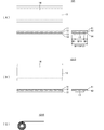
- FIG. 2A is a three-sided view of the high-frequency dielectric material 101 according to the first embodiment.
- FIG. 2B is a three-side view of another high frequency dielectric adhering material 101R according to the first embodiment.
- FIG. 2C is a side view of the entire high-frequency dielectric adhering material 101R wound in a roll shape.
- FIG. 3A is a perspective view of an antenna 201A that is an object of the high-frequency dielectric adhering material 101 according to the first embodiment.
- FIG. 3B is a perspective view of the antenna 201B in which the high-frequency dielectric material 101 is attached to the antenna 201A.
- FIG. 6A is a plan view of an antenna power feeding circuit unit that is an object of the high-frequency dielectric adhering material 102 according to the second embodiment.
- FIG. 6B is a plan view of a state in which the high-frequency dielectric adhering material 102 is attached to the antenna feeding circuit portion.
- FIG. 7A is a frequency characteristic diagram of the return loss of the antenna feeding unit shown in FIGS. 6A and 6B.
- FIG. 7B shows a return loss characteristic on the Smith chart before application of the high-frequency dielectric material 102
- FIG. 7C shows a return when the high-frequency dielectric material 102 is applied. It is the figure which represented the loss characteristic on the Smith chart.
- FIG. 8A is a plan view of the high-frequency dielectric material 103 according to the third embodiment.
- FIG. 8B is a front view of the high-frequency dielectric adhering material 103 in the thickness direction.
- FIG. 8C is a side view of the entire high frequency dielectric adhering material 103R when wound in a roll shape.
- FIG. 2A is a three-sided view of the high-frequency dielectric material 101 according to the first embodiment.
- the high-frequency dielectric adhering material 101 is a laminate of an insulating sheet layer 11, an adhesive layer 12, a dielectric sheet layer 13, and a release paper (release paper) 14.
- the insulator sheet layer 11 constitutes the outermost layer (upper layer in the direction of FIG. 2A), and the adhesive layer 12, the dielectric sheet layer 13, and the release paper 14 are arranged in that order under the insulator sheet layer 11. ing.
- the width W13 of the dielectric sheet layer 13 is narrower than the width W11 of the insulating sheet layer 11 and the width W12 of the adhesive layer 12, and the adhesive layer 12 protrudes in the width direction from the dielectric sheet layer 13.
- the release paper 14 When using the high-frequency dielectric material 101, the release paper 14 is peeled off, and the peeled surface is affixed to the object. In a state where the release paper 14 is peeled off, a portion of the adhesive layer 12 that protrudes in the width direction of the dielectric sheet layer 13 is exposed.
- the dimension W1 in the figure represents the width of the exposed portion of the adhesive layer 12.
- the dielectric sheet layer 13 is, for example, a mixture of LCP (liquid crystal polymer) and dielectric ceramic powder, and has a thickness of 5 to 50 ⁇ m.
- the exposed part of the adhesive layer 12 is adhered to the peripheral part other than the main part (center part) of the object. That is, the dielectric sheet layer 13 is in direct contact with the main part of the object, and the adhesive layer 12 is separated from the main part of the object. Therefore, the main part of the object is hardly affected by the low Q value and the low dielectric constant of the adhesive layer 12.
- FIG. 2B is a three-side view of another high frequency dielectric adhering material 101R according to the first embodiment.
- FIG. 2C is a side view of the entire high frequency dielectric adhering material 101R wound in a roll shape.
- FIG. 2 (A) a state in which the object is cut to a size corresponding to the application range of the object that is the application destination is shown, but FIG. A part of the state in which the direction is wound in a roll shape is shown.
- the high-frequency dielectric adhering material 101 ⁇ / b> R is a laminated body of the insulating sheet layer 11, the adhesive layer 12 and the dielectric sheet layer 13.
- the insulating sheet layer 11 constitutes the outermost layer (upper layer in the direction of FIG. 2B), and the adhesive layer 12 and the dielectric sheet layer 13 are sequentially disposed below the insulating sheet layer 11.
- the width W13 of the dielectric sheet layer 13 is narrower than the width W11 of the insulating sheet layer 11 and the width W12 of the adhesive layer 12, and the adhesive layer 12 protrudes in the width direction from the dielectric sheet layer 13.
- the outer surface of the insulator sheet layer 11 has releasability. Therefore, there is no release paper 14 as shown in FIG. 2A, and the paper is wound in a roll shape with the three-layer structure of the insulating sheet layer 11, the adhesive layer 12, and the dielectric sheet layer 13.
- the high-frequency dielectric adhering material 101R like a general adhesive tape, it is pulled out from a roll by a predetermined length, cut with a cutter, and attached to an object. In addition, you may wind in roll shape with the 4 layer structure provided with the release paper.
- FIG. 3A is a perspective view of an antenna 201A that is an object of the high-frequency dielectric adhering material 101 according to the first embodiment.
- FIG. 3B is a perspective view of the antenna 201B in which the high-frequency dielectric material 101 is attached to the antenna 201A.
- An antenna 201A as a frequency adjustment object is formed with a first radiation electrode (22A, 22B, 22C) and a second radiation electrode (23A, 23B, 23C, 23D) on the outer surface of a rectangular parallelepiped dielectric substrate 21.
- the feeding electrode FP and the ground electrode GND extend at predetermined positions of these radiation electrodes.
- the first radiation electrode 22C and the second radiation electrode 23D are partially opposed to each other in parallel, and constitute an open-ended capacitance. This structure constitutes a so-called branched inverted F-type antenna.
- the capacity of the antenna radiation electrode increases when the high-frequency dielectric adhering material 101 is affixed to the opposing portion of the first radiation electrode 22C and the second radiation electrode 23D. . Therefore, the resonance frequency is lowered.
- the dielectric sheet layer of the high-frequency dielectric adhering material 101 is disposed in a region where the electric field strength is high, and the exposed portion of the adhesive layer adheres to a region where the electric field strength is relatively low. become.
- FIG. 4 is a frequency characteristic diagram of the return loss of the antenna 201A shown in FIG. 3A and the antenna 201B shown in FIG.
- the dielectric sheet layer 13 of the high-frequency dielectric adhering material 101 has a thickness of 20 ⁇ m and a relative dielectric constant of 11.
- return loss occurs in two frequency bands, a low band and a high band.
- a return loss dip DIPLa is generated in the low band and a return loss dip DIPHa is generated in the high band.
- the center frequencies of the low-frequency return loss dip DIPLb and the high-frequency return loss dip DIPHb shift in the decreasing direction by applying the high-frequency dielectric adhesion material 101.
- the center frequency of the low-frequency return loss is shifted by 20 MHz
- the center frequency of the high-frequency return loss is shifted by 40 MHz.
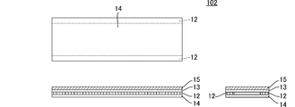
- FIG. 5 is a three-side view of the high-frequency dielectric material 102 according to the second embodiment.
- the high-frequency dielectric adhering material 102 is a laminate of the conductor sheet layer 15, the dielectric sheet layer 13, the adhesive layer 12, and the release paper 14.
- the conductor sheet layer 15 constitutes the outermost layer (upper layer in the direction of FIG. 5), and the dielectric sheet layer 13, the adhesive layer 12, and the release paper 14 are sequentially disposed below the conductor sheet layer 15.
- the pressure-sensitive adhesive layer 12 is disposed in the peripheral portion excluding the central portion of the dielectric sheet layer 13.
- the release paper 14 When using the high-frequency dielectric adhering material 102, the release paper 14 is peeled off, and the peeled surface is attached to the object. The adhesive layer 12 is exposed with the release paper peeled off.
- FIG. 6A is a plan view of an antenna feeding circuit unit that is an object of the high-frequency dielectric adhering material 102 according to the second embodiment.
- FIG. 6B is a plan view of a state in which the high-frequency dielectric adhering material 102 is attached to the antenna feeding circuit portion.
- a coplanar line including a ground electrode 31 and a center electrode 32 is formed on the substrate 30.
- This coplanar line is a power feeding circuit for the helical antenna 33.
- antenna impedance matching is important.
- the substrate 30 is a glass / epoxy substrate having a thickness of 1 mm
- the center electrode 32 has a line length of 37 mm, a line width of 1.5 mm
- the helical antenna 33 has a diameter of 10 mm, a length of 20 mm, and a copper of 1 mm in diameter.
- the wire is formed into a helical shape.
- the high frequency dielectric adhering material 102 shown in FIG. 5 When the impedance matching is adjusted using the high frequency dielectric adhering material 102 shown in FIG. 5, the high frequency dielectric adhering material 102 is affixed to the connection portion between the coplanar line and the helical antenna 33. As a result, a capacitance is provided between the center electrode 32 and the ground electrode 31, and the impedance of the coplanar line can be adjusted in a decreasing direction.
- FIG. 7 (A) is a frequency characteristic diagram of the return loss of the antenna feeding section shown in FIGS. 6 (A) and 6 (B).
- FIG. 7B shows a return loss characteristic on the Smith chart before application of the high-frequency dielectric material 102
- FIG. 7C shows a return when the high-frequency dielectric material 102 is applied. It is the figure which represented the loss characteristic on the Smith chart. Both represent the frequency range of 700 MHz to 2300 MHz.
- the return loss RLa is a characteristic before the high frequency dielectric adhering material 102 is affixed
- the return loss RLb is a characteristic in a state where the high frequency dielectric adhering material 102 is affixed.
- the frequency f1 is the center frequency of the low-frequency return loss
- the frequency f2 is the center frequency of the high-frequency return loss.
- the electrode of the object and the conductor sheet layer face each other in the thickness direction, thereby generating a large capacity. Therefore, the adjustment effect is high even if the size of the high-frequency dielectric adhering material 102 is relatively small, and impedance matching can be achieved at a local portion of the line.
- FIG. 8A is a plan view of the high-frequency dielectric material 103 according to the third embodiment.
- FIG. 8B is a front view of the high-frequency dielectric adhering material 103 in the thickness direction.
- FIG. 8C is a side view of the entire high frequency dielectric adhering material 103R when wound in a roll shape.
- the high-frequency dielectric adhering material 103 is a laminate of the conductor sheet layer 15, the adhesive layer 12, the dielectric sheet layer 13 and the release paper 14.
- the conductor sheet layer 15 constitutes the outermost layer (the bottom layer in the direction of FIG. 8), and the adhesive layer 12, the dielectric sheet layer 13, and the release paper 14 are arranged in order with respect to the conductor sheet layer 15.
- the conductor sheet layer 15 and the adhesive layer 12 are continuous bodies.
- the dielectric sheet layer 13 is adhered and held on the adhesive layer 12 individually.
- the conductor sheet layer 15 and the pressure-sensitive adhesive layer 12 are formed with half-cut slits by dividing lines indicated by broken lines in the drawing. Therefore, the laminated body of the conductor sheet layer 15, the adhesive layer 12, and the dielectric sheet layer 13 is separated by a dividing line indicated by a broken line in the drawing.
- the vertical and horizontal widths of the dielectric sheet layer 13 are narrower than the width divided by the dividing lines. Therefore, the adhesive layer 12 protrudes in the width direction from the dielectric sheet layer 13.
- the high-frequency dielectric material 103 can be used individually by partially peeling the release paper 14 and separating the laminate of the conductor sheet layer 15, the adhesive layer 12, and the dielectric sheet layer 13 by dividing lines. it can. Thus, a laminated body can be divided
- the release paper 14 is partially removed while the high-frequency dielectric adhering material 103R is pulled out from the roll body.
- the laminate of the conductor sheet layer 15, the adhesive layer 12, and the dielectric sheet layer 13 is separated by a dividing line and used individually.
Landscapes
- Physics & Mathematics (AREA)
- Electromagnetism (AREA)
- Engineering & Computer Science (AREA)
- Manufacturing & Machinery (AREA)
- Laminated Bodies (AREA)
- Adhesive Tapes (AREA)
- Insulating Bodies (AREA)
- Details Of Aerials (AREA)
Abstract
Description
このように誘電体基板1の表面に形成された共振器3を覆うように誘電体テープ6を貼付することによって、フィルタの中心周波数の調整を行うことができる。
(1)絶縁体シート層、粘着層、及び誘電体シート層の積層体であり、絶縁体シート層が最外層を構成し、絶縁体シート層の下層に粘着層及び誘電体シート層が順に配置され、誘電体シート層の幅が絶縁体シート層及び粘着層の幅よりも狭く、粘着層が誘電体シート層よりも幅方向にはみ出ている。すなわち、その部分が露出している。
第1の実施形態に係る高周波用誘電体付着材について、図2~図4を参照して説明する。
図2(A)は、第1の実施形態に係る高周波用誘電体付着材101の三面図である。但し、積層構造を明瞭にするために、厚み方向は多少拡大して描いている。高周波用誘電体付着材101は、絶縁体シート層11、粘着層12、誘電体シート層13及び剥離紙(離型紙)14の積層体である。絶縁体シート層11は最外層(図2(A)の向きで上面の層)を構成し、絶縁体シート層11の下層に粘着層12、誘電体シート層13及び剥離紙14が順に配置されている。誘電体シート層13の幅W13は絶縁体シート層11の幅W11及び粘着層12の幅W12よりも狭く、粘着層12が誘電体シート層13よりも幅方向にはみ出ている。
なお、剥離紙を備えた4層構造のままロール状に巻回してもよい。
図5は、第2の実施形態に係る高周波用誘電体付着材102の三面図である。但し、積層構造を明瞭にするために、厚み方向は多少拡大して描いている。高周波用誘電体付着材102は、導電体シート層15、誘電体シート層13、粘着層12、及び剥離紙14の積層体である。導電体シート層15は最外層(図5の向きで上面の層)を構成し、導電体シート層15の下層に誘電体シート層13、粘着層12及び剥離紙14が順に配置されている。粘着層12は誘電体シート層13の中央部を除く周辺部に配置されている。
図8(A)は、第3の実施形態に係る高周波用誘電体付着材103の平面図である。図8(B)は、高周波用誘電体付着材103の厚み方向の正面図である。図8(C)は、ロール状に巻回した場合の高周波用誘電体付着材103Rの全体の側面図である。高周波用誘電体付着材103は、導電体シート層15、粘着層12、誘電体シート層13及び剥離紙14の積層体である。導電体シート層15は最外層(図8の向きで下面の層)を構成し、導電体シート層15に対して粘着層12、誘電体シート層13及び剥離紙14が順に配置されている。
第3の実施形態では、積層体が二次元に広がり、分割ラインが縦横に形成された例を示したが、第1の実施形態で図2(C)に示したようにロール状にして使用する場合には、積層体に一定長ごとのハーフカットの分割ラインを入れておいてもよい。
12…粘着層
13…誘電体シート層
14…剥離紙
15…導電体シート層
21…誘電体基体
22A,22B,22C…放射電極
23A,23B,23C,23D…放射電極
30…基板
31…グランド電極
32…中心電極
33…ヘリカルアンテナ
101,101R…高周波用誘電体付着材
102,103…高周波用誘電体付着材
201A,201B…アンテナ
Claims (6)
- 絶縁体シート層、粘着層、及び誘電体シート層の積層体である高周波用誘電体付着材であって、
前記絶縁体シート層が最外層を構成し、前記絶縁体シート層の下層に前記粘着層及び前記誘電体シート層が順に配置され、前記誘電体シート層の幅が前記絶縁体シート層及び前記粘着層の幅よりも狭く、前記粘着層が前記誘電体シート層よりも幅方向にはみ出ている高周波用誘電体付着材。 - 導電体シート層、粘着層、及び誘電体シート層の積層体である高周波用誘電体付着材であって、
前記導電体シート層が最外層を構成し、前記導電体シート層の下層に前記粘着層及び前記誘電体シート層が順に配置され、前記誘電体シート層の幅が前記導電体シート層及び前記粘着層の幅よりも狭く、前記粘着層が前記誘電体シート層よりも幅方向にはみ出ている高周波用誘電体付着材。 - 導電体シート層、誘電体シート層、及び粘着層の積層体である高周波用誘電体付着材であって、
前記導電体シート層が最外層を構成し、前記導電体シート層の下層に前記誘電体シート層及び前記粘着層が順に配置され、前記粘着層は前記誘電体シート層の中央部を除く周辺部に配置されている高周波用誘電体付着材。 - 前記積層体は前記誘電体シート層の幅を有し、長手方向がロール状に巻かれた、請求項1乃至3の何れかに記載の高周波用誘電体付着材。
- 前記積層体には、少なくとも前記粘着層の露出部を覆う剥離紙を備えた、請求項1乃至4の何れかに記載の高周波用誘電体付着材。
- 前記積層体は一定長さ又は一定サイズでハーフカットされている、請求項1乃至5の何れかに記載の高周波用誘電体付着材。
Priority Applications (3)
| Application Number | Priority Date | Filing Date | Title |
|---|---|---|---|
| JP2012501625A JP5522250B2 (ja) | 2010-02-26 | 2010-10-26 | 高周波用誘電体付着材 |
| CN201080064042.1A CN102763266B (zh) | 2010-02-26 | 2010-10-26 | 高频用电介质附着材料 |
| US13/594,755 US8658267B2 (en) | 2010-02-26 | 2012-08-24 | High-frequency dielectric attachment |
Applications Claiming Priority (2)
| Application Number | Priority Date | Filing Date | Title |
|---|---|---|---|
| JP2010-041189 | 2010-02-26 | ||
| JP2010041189 | 2010-02-26 |
Related Child Applications (1)
| Application Number | Title | Priority Date | Filing Date |
|---|---|---|---|
| US13/594,755 Continuation US8658267B2 (en) | 2010-02-26 | 2012-08-24 | High-frequency dielectric attachment |
Publications (1)
| Publication Number | Publication Date |
|---|---|
| WO2011104932A1 true WO2011104932A1 (ja) | 2011-09-01 |
Family
ID=44506370
Family Applications (1)
| Application Number | Title | Priority Date | Filing Date |
|---|---|---|---|
| PCT/JP2010/068888 Ceased WO2011104932A1 (ja) | 2010-02-26 | 2010-10-26 | 高周波用誘電体付着材 |
Country Status (4)
| Country | Link |
|---|---|
| US (1) | US8658267B2 (ja) |
| JP (1) | JP5522250B2 (ja) |
| CN (1) | CN102763266B (ja) |
| WO (1) | WO2011104932A1 (ja) |
Cited By (1)
| Publication number | Priority date | Publication date | Assignee | Title |
|---|---|---|---|---|
| JP2016178488A (ja) * | 2015-03-20 | 2016-10-06 | カシオ計算機株式会社 | アンテナ装置及び電子機器 |
Families Citing this family (3)
| Publication number | Priority date | Publication date | Assignee | Title |
|---|---|---|---|---|
| JPH0667568B2 (ja) | 1986-12-23 | 1994-08-31 | 松下電工株式会社 | 繊維セメント板の製造法 |
| CN106377957A (zh) * | 2016-11-18 | 2017-02-08 | 苏州康喜医疗净化设备有限公司 | 空气净化过滤棉 |
| KR20240008681A (ko) * | 2022-07-12 | 2024-01-19 | 에스케이하이닉스 주식회사 | 반도체 장치 |
Citations (4)
| Publication number | Priority date | Publication date | Assignee | Title |
|---|---|---|---|---|
| JPH07504280A (ja) * | 1991-07-09 | 1995-05-11 | メト・インターナツィオナール・ゲーエムベーハー | 盗難防止用マーカ |
| JP2005198168A (ja) * | 2004-01-09 | 2005-07-21 | Toppan Forms Co Ltd | 非接触型情報記録媒体及びこれを用いたラベル |
| JP2008112441A (ja) * | 2006-10-05 | 2008-05-15 | Dainippon Printing Co Ltd | 非接触icタグと非接触icタグのエンコード方法 |
| JP2008191927A (ja) * | 2007-02-05 | 2008-08-21 | Brother Ind Ltd | 無線タグラベル及びタグテープ |
Family Cites Families (11)
| Publication number | Priority date | Publication date | Assignee | Title |
|---|---|---|---|---|
| US4298642A (en) * | 1978-01-25 | 1981-11-03 | Walter John W | Self-adhesive crossover foil of metal and polyester |
| JPS607528Y2 (ja) | 1979-12-24 | 1985-03-14 | 株式会社村田製作所 | ストリツプ線路フイルタ |
| FR2547116B1 (fr) * | 1983-05-31 | 1985-10-25 | Thomson Csf | Procede d'ajustage notamment en frequence d'un filtre imprime en ligne " microbandes ", et filtre obtenu par ce procede |
| JPH09238002A (ja) * | 1996-02-29 | 1997-09-09 | Nec Corp | マイクロストリップフィルタとその中心周波数調整方法 |
| DE69941734D1 (de) * | 1999-08-27 | 2010-01-07 | Hitachi Ltd | Isoliermaterial, elektrische wicklung und herstellungsmethode |
| US7091422B1 (en) * | 2005-01-28 | 2006-08-15 | Multek Flexible Circuits, Inc. | Flexible flat cable with insulating layer having distinct adhesives on opposing faces |
| JP5433416B2 (ja) * | 2006-08-08 | 2014-03-05 | ワールド プラパティーズ、 インコーポレイテッド | 回路材料、回路および多層回路積層板 |
| JP2008270370A (ja) * | 2007-04-17 | 2008-11-06 | Taiyo Yuden Co Ltd | 電磁波遮蔽シート |
| US8231614B2 (en) * | 2007-05-11 | 2012-07-31 | Tyco Healthcare Group Lp | Temperature monitoring return electrode |
| JP5200557B2 (ja) * | 2008-01-25 | 2013-06-05 | 株式会社村田製作所 | 無線icデバイスの製造方法 |
| CN201465165U (zh) * | 2009-07-02 | 2010-05-12 | 上海韩硕信息科技有限公司 | 一种电子防伪标签以及电子防伪标签带 |
-
2010
- 2010-10-26 JP JP2012501625A patent/JP5522250B2/ja active Active
- 2010-10-26 CN CN201080064042.1A patent/CN102763266B/zh active Active
- 2010-10-26 WO PCT/JP2010/068888 patent/WO2011104932A1/ja not_active Ceased
-
2012
- 2012-08-24 US US13/594,755 patent/US8658267B2/en active Active
Patent Citations (4)
| Publication number | Priority date | Publication date | Assignee | Title |
|---|---|---|---|---|
| JPH07504280A (ja) * | 1991-07-09 | 1995-05-11 | メト・インターナツィオナール・ゲーエムベーハー | 盗難防止用マーカ |
| JP2005198168A (ja) * | 2004-01-09 | 2005-07-21 | Toppan Forms Co Ltd | 非接触型情報記録媒体及びこれを用いたラベル |
| JP2008112441A (ja) * | 2006-10-05 | 2008-05-15 | Dainippon Printing Co Ltd | 非接触icタグと非接触icタグのエンコード方法 |
| JP2008191927A (ja) * | 2007-02-05 | 2008-08-21 | Brother Ind Ltd | 無線タグラベル及びタグテープ |
Cited By (1)
| Publication number | Priority date | Publication date | Assignee | Title |
|---|---|---|---|---|
| JP2016178488A (ja) * | 2015-03-20 | 2016-10-06 | カシオ計算機株式会社 | アンテナ装置及び電子機器 |
Also Published As
| Publication number | Publication date |
|---|---|
| US8658267B2 (en) | 2014-02-25 |
| JP5522250B2 (ja) | 2014-06-18 |
| CN102763266A (zh) | 2012-10-31 |
| JPWO2011104932A1 (ja) | 2013-06-17 |
| US20120321831A1 (en) | 2012-12-20 |
| CN102763266B (zh) | 2014-10-22 |
Similar Documents
| Publication | Publication Date | Title |
|---|---|---|
| US10418708B2 (en) | Wideband antenna | |
| US9190732B2 (en) | Antenna device | |
| JP5408160B2 (ja) | 水平方向放射アンテナ | |
| US9172142B2 (en) | Horizontal radiation antenna | |
| EP1768211A1 (en) | Flat-plate mimo array antenna with an isolation element | |
| US7460072B1 (en) | Miniature patch antenna with increased gain | |
| JP2008294491A (ja) | アンテナ装置 | |
| KR20170036339A (ko) | 벤딩 내구성이 개선된 연성회로기판 | |
| KR20170036364A (ko) | 3층 유전체 및 4층 그라운드 레이어 구조를 갖는 연성회로기판 | |
| JP5522250B2 (ja) | 高周波用誘電体付着材 | |
| WO2019107382A1 (ja) | アンテナ装置 | |
| JP2000244232A (ja) | マイクロストリップアンテナ | |
| EP3891844B1 (en) | Slot antenna and electronic device comprising said slot antenna | |
| US11152706B2 (en) | Antenna device | |
| JP5864468B2 (ja) | 誘電体導波管入出力構造 | |
| US11394100B2 (en) | High-frequency connection structure for connecting a coaxial line to a planar line using adhesion layers | |
| KR20170067610A (ko) | 고주파 전송선로 | |
| JP3421334B2 (ja) | Icタグ | |
| JPH08181531A (ja) | レドーム付きスロット結合マイクロストリップアンテナ | |
| JPH04170804A (ja) | マイクロストリップアンテナ | |
| US7333069B2 (en) | Radiating element designed to operate in a small antenna | |
| KR200407013Y1 (ko) | 선형배열 패치 안테나에서 주파수 대역폭을 증가시키기 위한 계단형 접지판 | |
| TW494606B (en) | Dual-beam microstripe antenna | |
| WO2009004605A2 (en) | Miniature patch antenna with increased gain | |
| JP2007088917A (ja) | 伝送線路、電子部品及び伝送線路の製造方法 |
Legal Events
| Date | Code | Title | Description |
|---|---|---|---|
| WWE | Wipo information: entry into national phase |
Ref document number: 201080064042.1 Country of ref document: CN |
|
| 121 | Ep: the epo has been informed by wipo that ep was designated in this application |
Ref document number: 10846595 Country of ref document: EP Kind code of ref document: A1 |
|
| WWE | Wipo information: entry into national phase |
Ref document number: 2012501625 Country of ref document: JP |
|
| NENP | Non-entry into the national phase |
Ref country code: DE |
|
| 122 | Ep: pct application non-entry in european phase |
Ref document number: 10846595 Country of ref document: EP Kind code of ref document: A1 |