WO2011104894A1 - 薄膜半導体装置、薄膜半導体製造装置及び薄膜半導体製造方法 - Google Patents
薄膜半導体装置、薄膜半導体製造装置及び薄膜半導体製造方法 Download PDFInfo
- Publication number
- WO2011104894A1 WO2011104894A1 PCT/JP2010/053511 JP2010053511W WO2011104894A1 WO 2011104894 A1 WO2011104894 A1 WO 2011104894A1 JP 2010053511 W JP2010053511 W JP 2010053511W WO 2011104894 A1 WO2011104894 A1 WO 2011104894A1
- Authority
- WO
- WIPO (PCT)
- Prior art keywords
- thin film
- semiconductor device
- roll
- film semiconductor
- semiconductor layer
- Prior art date
- Legal status (The legal status is an assumption and is not a legal conclusion. Google has not performed a legal analysis and makes no representation as to the accuracy of the status listed.)
- Ceased
Links
Images




Classifications
-
- H—ELECTRICITY
- H10—SEMICONDUCTOR DEVICES; ELECTRIC SOLID-STATE DEVICES NOT OTHERWISE PROVIDED FOR
- H10D—INORGANIC ELECTRIC SEMICONDUCTOR DEVICES
- H10D30/00—Field-effect transistors [FET]
- H10D30/60—Insulated-gate field-effect transistors [IGFET]
- H10D30/67—Thin-film transistors [TFT]
- H10D30/674—Thin-film transistors [TFT] characterised by the active materials
- H10D30/6755—Oxide semiconductors, e.g. zinc oxide, copper aluminium oxide or cadmium stannate
-
- G—PHYSICS
- G02—OPTICS
- G02F—OPTICAL DEVICES OR ARRANGEMENTS FOR THE CONTROL OF LIGHT BY MODIFICATION OF THE OPTICAL PROPERTIES OF THE MEDIA OF THE ELEMENTS INVOLVED THEREIN; NON-LINEAR OPTICS; FREQUENCY-CHANGING OF LIGHT; OPTICAL LOGIC ELEMENTS; OPTICAL ANALOGUE/DIGITAL CONVERTERS
- G02F1/00—Devices or arrangements for the control of the intensity, colour, phase, polarisation or direction of light arriving from an independent light source, e.g. switching, gating or modulating; Non-linear optics
- G02F1/01—Devices or arrangements for the control of the intensity, colour, phase, polarisation or direction of light arriving from an independent light source, e.g. switching, gating or modulating; Non-linear optics for the control of the intensity, phase, polarisation or colour
- G02F1/13—Devices or arrangements for the control of the intensity, colour, phase, polarisation or direction of light arriving from an independent light source, e.g. switching, gating or modulating; Non-linear optics for the control of the intensity, phase, polarisation or colour based on liquid crystals, e.g. single liquid crystal display cells
- G02F1/133—Constructional arrangements; Operation of liquid crystal cells; Circuit arrangements
- G02F1/136—Liquid crystal cells structurally associated with a semi-conducting layer or substrate, e.g. cells forming part of an integrated circuit
- G02F1/1362—Active matrix addressed cells
- G02F1/1368—Active matrix addressed cells in which the switching element is a three-electrode device
-
- H—ELECTRICITY
- H10—SEMICONDUCTOR DEVICES; ELECTRIC SOLID-STATE DEVICES NOT OTHERWISE PROVIDED FOR
- H10D—INORGANIC ELECTRIC SEMICONDUCTOR DEVICES
- H10D30/00—Field-effect transistors [FET]
- H10D30/01—Manufacture or treatment
- H10D30/021—Manufacture or treatment of FETs having insulated gates [IGFET]
- H10D30/031—Manufacture or treatment of FETs having insulated gates [IGFET] of thin-film transistors [TFT]
-
- H—ELECTRICITY
- H10—SEMICONDUCTOR DEVICES; ELECTRIC SOLID-STATE DEVICES NOT OTHERWISE PROVIDED FOR
- H10D—INORGANIC ELECTRIC SEMICONDUCTOR DEVICES
- H10D30/00—Field-effect transistors [FET]
- H10D30/60—Insulated-gate field-effect transistors [IGFET]
- H10D30/67—Thin-film transistors [TFT]
- H10D30/6758—Thin-film transistors [TFT] characterised by the insulating substrates
-
- H—ELECTRICITY
- H10—SEMICONDUCTOR DEVICES; ELECTRIC SOLID-STATE DEVICES NOT OTHERWISE PROVIDED FOR
- H10D—INORGANIC ELECTRIC SEMICONDUCTOR DEVICES
- H10D86/00—Integrated devices formed in or on insulating or conducting substrates, e.g. formed in silicon-on-insulator [SOI] substrates or on stainless steel or glass substrates
- H10D86/40—Integrated devices formed in or on insulating or conducting substrates, e.g. formed in silicon-on-insulator [SOI] substrates or on stainless steel or glass substrates characterised by multiple TFTs
- H10D86/411—Integrated devices formed in or on insulating or conducting substrates, e.g. formed in silicon-on-insulator [SOI] substrates or on stainless steel or glass substrates characterised by multiple TFTs characterised by materials, geometry or structure of the substrates
-
- H—ELECTRICITY
- H10—SEMICONDUCTOR DEVICES; ELECTRIC SOLID-STATE DEVICES NOT OTHERWISE PROVIDED FOR
- H10D—INORGANIC ELECTRIC SEMICONDUCTOR DEVICES
- H10D86/00—Integrated devices formed in or on insulating or conducting substrates, e.g. formed in silicon-on-insulator [SOI] substrates or on stainless steel or glass substrates
- H10D86/40—Integrated devices formed in or on insulating or conducting substrates, e.g. formed in silicon-on-insulator [SOI] substrates or on stainless steel or glass substrates characterised by multiple TFTs
- H10D86/421—Integrated devices formed in or on insulating or conducting substrates, e.g. formed in silicon-on-insulator [SOI] substrates or on stainless steel or glass substrates characterised by multiple TFTs having a particular composition, shape or crystalline structure of the active layer
- H10D86/423—Integrated devices formed in or on insulating or conducting substrates, e.g. formed in silicon-on-insulator [SOI] substrates or on stainless steel or glass substrates characterised by multiple TFTs having a particular composition, shape or crystalline structure of the active layer comprising semiconductor materials not belonging to the Group IV, e.g. InGaZnO
-
- H—ELECTRICITY
- H10—SEMICONDUCTOR DEVICES; ELECTRIC SOLID-STATE DEVICES NOT OTHERWISE PROVIDED FOR
- H10D—INORGANIC ELECTRIC SEMICONDUCTOR DEVICES
- H10D86/00—Integrated devices formed in or on insulating or conducting substrates, e.g. formed in silicon-on-insulator [SOI] substrates or on stainless steel or glass substrates
- H10D86/40—Integrated devices formed in or on insulating or conducting substrates, e.g. formed in silicon-on-insulator [SOI] substrates or on stainless steel or glass substrates characterised by multiple TFTs
- H10D86/60—Integrated devices formed in or on insulating or conducting substrates, e.g. formed in silicon-on-insulator [SOI] substrates or on stainless steel or glass substrates characterised by multiple TFTs wherein the TFTs are in active matrices
-
- H—ELECTRICITY
- H10—SEMICONDUCTOR DEVICES; ELECTRIC SOLID-STATE DEVICES NOT OTHERWISE PROVIDED FOR
- H10D—INORGANIC ELECTRIC SEMICONDUCTOR DEVICES
- H10D99/00—Subject matter not provided for in other groups of this subclass
-
- H—ELECTRICITY
- H10—SEMICONDUCTOR DEVICES; ELECTRIC SOLID-STATE DEVICES NOT OTHERWISE PROVIDED FOR
- H10P—GENERIC PROCESSES OR APPARATUS FOR THE MANUFACTURE OR TREATMENT OF DEVICES COVERED BY CLASS H10
- H10P14/00—Formation of materials, e.g. in the shape of layers or pillars
- H10P14/20—Formation of materials, e.g. in the shape of layers or pillars of semiconductor materials
- H10P14/34—Deposited materials, e.g. layers
- H10P14/3402—Deposited materials, e.g. layers characterised by the chemical composition
- H10P14/3434—Deposited materials, e.g. layers characterised by the chemical composition being oxide semiconductor materials
-
- H—ELECTRICITY
- H10—SEMICONDUCTOR DEVICES; ELECTRIC SOLID-STATE DEVICES NOT OTHERWISE PROVIDED FOR
- H10P—GENERIC PROCESSES OR APPARATUS FOR THE MANUFACTURE OR TREATMENT OF DEVICES COVERED BY CLASS H10
- H10P14/00—Formation of materials, e.g. in the shape of layers or pillars
- H10P14/20—Formation of materials, e.g. in the shape of layers or pillars of semiconductor materials
- H10P14/29—Formation of materials, e.g. in the shape of layers or pillars of semiconductor materials characterised by the substrates
- H10P14/2901—Materials
- H10P14/2922—Materials being non-crystalline insulating materials, e.g. glass or polymers
-
- H—ELECTRICITY
- H10—SEMICONDUCTOR DEVICES; ELECTRIC SOLID-STATE DEVICES NOT OTHERWISE PROVIDED FOR
- H10P—GENERIC PROCESSES OR APPARATUS FOR THE MANUFACTURE OR TREATMENT OF DEVICES COVERED BY CLASS H10
- H10P14/00—Formation of materials, e.g. in the shape of layers or pillars
- H10P14/20—Formation of materials, e.g. in the shape of layers or pillars of semiconductor materials
- H10P14/32—Formation of materials, e.g. in the shape of layers or pillars of semiconductor materials characterised by intermediate layers between substrates and deposited layers
- H10P14/3202—Materials thereof
- H10P14/3238—Materials thereof being insulating materials
-
- H—ELECTRICITY
- H10—SEMICONDUCTOR DEVICES; ELECTRIC SOLID-STATE DEVICES NOT OTHERWISE PROVIDED FOR
- H10P—GENERIC PROCESSES OR APPARATUS FOR THE MANUFACTURE OR TREATMENT OF DEVICES COVERED BY CLASS H10
- H10P14/00—Formation of materials, e.g. in the shape of layers or pillars
- H10P14/20—Formation of materials, e.g. in the shape of layers or pillars of semiconductor materials
- H10P14/34—Deposited materials, e.g. layers
- H10P14/3402—Deposited materials, e.g. layers characterised by the chemical composition
Definitions
- the present invention relates to a thin film semiconductor device, a thin film semiconductor manufacturing apparatus, and a thin film semiconductor manufacturing method, which are flexible displays using a plastic substrate.
- TFTs Thin film semiconductor devices for image driving of displays have conventionally used a-Si as their semiconductor layers and are still in widespread use today.
- TFTs using a-Si 2 as a semiconductor layer have a very small field effect mobility ( ⁇ 0.1 cm 2 / Vs), so that they have high functions such as high-definition video, which has been rapidly demanded in recent years. The application was reaching its performance limit.
- any of the Si-based TFTs described above has a relatively high semiconductor layer deposition temperature, it exceeds the heat resistance temperature of plastic substrates and roll film substrates used for flexible displays, etc. There was also a problem that it was difficult.
- InGaZnOx-based oxide semiconductors have been studied as a new material that can replace them. Since this InGaZnOx-based oxide semiconductor can be formed by a non-vacuum / low-temperature process such as sputtering, the InGaZnOx-based oxide semiconductor can be formed on a flexible substrate, and the process is also low in cost. This oxide semiconductor is still insufficient in performance as it is after low-temperature process film formation, and sufficient performance can be obtained by performing baking by annealing after film formation. In the case of furnace annealing, about 300 ° C. is necessary for baking, which causes problems such as thermal expansion deformation of the flexible substrate (although the heat resistance temperature is not exceeded).
- the oxide semiconductor is maintained in an amorphous state, so there is no fear of variation due to grain boundaries as in the case of poly-Si described above, and field-effect mobility ( ⁇ 10 cm 2 / Vs). It has many advantages over Si, such as being relatively high and capable of handling high-definition video.
- oxide semiconductors have problems with stability against heat and light.
- external light particularly light in the near-ultraviolet region with a wavelength of 500 nm or less
- the off-current of the TFT increases (the off-current increases by about two orders of magnitude at a wavelength of 370 nm), and the TFT threshold fluctuates by 5 V accordingly. Since the display has a structure in which backlights, external light, etc. are likely to enter the TFT, such a characteristic variation can be a very serious problem in circuit operation.
- a light shielding layer made of metal (sometimes shared with wiring) is provided above and below the TFT. Because it is difficult to completely block the stray light, it is not a complete measure.
- an oxide semiconductor is sensitive to heat, and even if it is baked by annealing after film formation as described above, the off-state current increases and the threshold value increases when the usage environment reaches 100 ° C. or higher. Shift about 5V. This shift amount becomes more conspicuous as the use environment temperature is higher, and the transistor cannot be switched at 200 ° C. or higher. This is considered to be caused by a change in the bonding state between oxygen and another element in the oxide semiconductor due to heat. This change is reversible, and if the use environment is restored, the TFT characteristics will be restored to a few tens of minutes, but there is no doubt that this is a major problem for display applications.
- the present invention has been made in consideration of the above points, can be formed by a low-temperature process, can realize a low process cost, can realize a relatively high field-effect mobility, and is resistant to light and heat.
- An object of the present invention is to propose a thin film semiconductor device, a thin film semiconductor manufacturing apparatus, and a thin film semiconductor manufacturing method that have stable characteristics and can be applied to a bending environment.
- the present invention is configured as follows.
- the invention according to claim 1 is a plastic substrate; A barrier layer formed on the plastic substrate; A semiconductor layer formed on the barrier layer; An insulating layer formed in contact with either upper or lower surface of the semiconductor layer; A metal layer formed in contact with the insulating layer; Have Using the semiconductor layer as a channel, the metal layer as a source electrode, a drain electrode, and a gate electrode, and the insulating layer as a gate insulating film,
- the semiconductor layer includes at least one of nonmetallic elements nitrogen (N) and oxygen (O), semimetallic elements boron (B), silicon (Si), germanium (Ge), arsenic (As), and antimony (Sb).
- the nonmetallic element is at least a mixture of oxygen (O) and nitrogen (N), and the ratio of nitrogen (N) to oxygen (O) (N number density / O number density) is 0 to 2. It is a thin film semiconductor device.
- the invention according to claim 3 is the thin film semiconductor device according to claim 1 or 2, wherein the plastic substrate is at least a roll-shaped film substrate.
- the invention according to claim 4 is the thin film semiconductor device according to any one of claims 1 to 3, wherein the semiconductor layer is amorphous.
- the invention according to claim 5 is the thin film semiconductor device according to any one of claims 1 to 4, wherein the band gap of the semiconductor layer is 1 eV to 5 eV.
- the main carrier of the semiconductor layer is an electron
- the carrier concentration is 1 ⁇ 10E 16 to 1 ⁇ 10E 21 (m ⁇ 3 ) in a thermal equilibrium state of 300K
- the field effect mobility is 0.1. It is 1 thru
- the invention according to claim 7 is the thin film semiconductor device according to any one of claims 1 to 6, wherein the semiconductor layer constitutes a circuit for driving a liquid crystal display device.
- the invention according to claim 8 is the roll film substrate, A barrier layer formed on the roll film substrate; A semiconductor layer formed on the barrier layer; An insulating layer formed in contact with either upper or lower surface of the semiconductor layer; A metal layer formed in contact with the insulating layer; Have Using the semiconductor layer as a channel, the metal layer as a source electrode, a drain electrode, and a gate electrode, and the insulating layer as a gate insulating film,
- the semiconductor layer includes at least one of nonmetallic elements nitrogen (N) and oxygen (O), semimetallic elements boron (B), silicon (Si), germanium (Ge), arsenic (As), and antimony (Sb).
- the non-metallic element is a mixture of at least oxygen (O) and nitrogen (N), and the ratio of nitrogen (N) to oxygen (O) (N number density / O number density) is 0 to 2 is sputtered.
- a thin film semiconductor manufacturing apparatus formed by the apparatus.
- Si silicon
- Ge germanium
- x 0 to 1 is established
- N nitrogen
- Si1-xGex N number density / Si1-xGex number density
- the invention according to claim 10 is characterized in that the sputtering apparatus comprises: A roll winding mechanism for mounting the roll film substrate; A delivery mechanism for delivering the roll-shaped film substrate from one end along the longitudinal direction; A winding mechanism for winding up the rolled film substrate that has been sent out; An alignment mechanism that performs planar alignment of the roll-shaped film substrate with respect to the roll-shaped film substrate having the alignment pattern, A metal target facing the semiconductor forming surface of the roll film substrate; Have 10.
- the invention according to claim 11 is characterized in that the sputtering apparatus comprises: A gas introduction mechanism for introducing an atmospheric gas containing the nonmetallic element into a vacuum chamber; A plurality of metal targets including the metal element or the metalloid element or a mixture thereof, The thin film semiconductor manufacturing apparatus according to claim 8 or 9, wherein the metal targets are arranged at linear positions along the length of the roll film substrate.
- the invention according to claim 12 is characterized in that the sputtering apparatus comprises: The mixture of a plurality of elements each including at least one of the non-metallic element, the metallic element, and the metalloid element is used as a single target. 2.
- Invention of Claim 13 uses the thin film semiconductor manufacturing apparatus of any one of Claim 8 thru
- the present invention has the following effects.
- the semiconductor layer of the thin film semiconductor device is used as a channel
- the metal layer is used as a source, drain, and gate
- the insulating layer is used as a gate insulating film
- the semiconductor layer includes nitrogen (N) of a nonmetallic element, At least one of oxygen (O), boron (B), silicon (Si), germanium (Ge), arsenic (As), antimony (Sb), tellurium (Te), polonium (Po) at least one of the metalloid elements
- One and the metal elements aluminum (Al), zinc (Zn), gallium (Ga), cadmium (Cd), indium (In), tin (Sn), mercury (Hg), thallium (Tl), terbium (Pb)
- Including at least one of bismuth (Bi), and the non-metallic element is a mixture of at least oxygen (O) and nitrogen (N), and nitrogen relative to oxygen (O) ( Ratio) (N number density / O
- the semiconductor layer can be formed by a low-temperature process of sputtering, and a low process cost can be realized.
- the ratio of nitrogen (N) to the mixture (Si1-xGex) (N number density / Si1-xGex number density) is 1 to 2, and a band is formed by introducing germanium (Ge) into the metalloid silicon (Si).
- the gap can be reduced, and this can be combined with the band gap increase by introducing nitrogen (N) in claim 1 to freely control the band gap and to increase the field effect mobility.
- the plastic substrate is at least a roll-shaped film substrate, and is wound from the roll state to the feed roll state at the time of manufacture, realizing a low process cost and providing a low-cost display. .
- the semiconductor layer is amorphous and has no grain boundary, thereby increasing the uniformity of characteristics and the bending strength when formed on a plastic substrate or a roll film substrate. Can be improved.
- the band gap of the semiconductor layer can be widened by introducing nitrogen (N) into the semiconductor layer.
- N nitrogen
- the band gap of the semiconductor layer can be widened by introducing nitrogen (N) into the semiconductor layer.
- N nitrogen
- the main carrier of the semiconductor layer is an electron
- the carrier concentration is 1 ⁇ 10E16 to 1 ⁇ 10E21 (m ⁇ 3 ) in a thermal equilibrium state of 300 K
- the field effect mobility is 0.1 to 50. (Cm 2 / Vs), and higher field-effect mobility can be obtained, so that even high-definition movies can be handled.
- the semiconductor layer constitutes a circuit for driving the liquid crystal display device, Compatible with active matrix liquid crystal display devices.
- the semiconductor layer by forming the semiconductor layer by a sputtering method, it can be formed by a low temperature process, a low process cost can be realized, a relatively high mobility can be realized, and light and heat can be realized. In contrast, a thin film semiconductor device having stable characteristics can be manufactured.
- the ninth aspect of the invention it is possible to manufacture a thin film semiconductor manufacturing apparatus capable of freely controlling the band gap and increasing the field effect mobility.
- the sputtering apparatus includes a vacuum chamber that holds all the mechanisms therein, and realizes a low process cost by using a roll-to-roll method of winding from a roll state to a feed roll state during manufacturing. be able to.
- the sputtering apparatus introduces an atmospheric gas containing a nonmetallic element into the vacuum chamber, and has a plurality of metal targets containing a metal element, a metalloid element, or a mixture thereof.
- a semiconductor layer having a uniform property can be formed in the roll film substrate by being arranged at linear positions along the length of the roll film substrate.
- the sputtering apparatus uses a mixture obtained by mixing a plurality of elements including at least one of a nonmetallic element, a metallic element, and a semimetallic element as a single target, and the properties of the semiconductor layer are adjusted. Furthermore, the sputtering process cost can be reduced while making it uniform.
- a thin film semiconductor device is manufactured using the thin film semiconductor manufacturing apparatus described in any one of claims 8 to 12.
- FIG. 1 It is sectional drawing explaining the structure of a thin film semiconductor device. It is a figure which shows the thin film semiconductor device formed on the roll-shaped film board
- FIG. 1 is a cross-sectional view illustrating the structure of a thin film semiconductor device.
- the thin film semiconductor device 1 has a plastic substrate 2, and barrier layers 3 and 4 are formed on both surfaces of the plastic substrate 2.
- a glass substrate 6 is provided on the upper surface of the barrier layer 3 formed on the plastic substrate 2 via an adhesive layer 5, and a semiconductor layer 7 is formed on the upper surface of the glass substrate 6.
- the glass substrate 6 is thinned from the original state having a certain thickness (about 0.5 mm) as a base for forming the semiconductor layer 7 by a process such as etching after the formation of the semiconductor layer 7 (0 .1 mm or less) and becomes unnecessary after the plastic substrate 2 and the semiconductor layer 7 are bonded via the adhesive layer 5. Therefore, in some cases, the glass substrate 6 may be completely removed by etching.
- the semiconductor layer 7 is formed on the barrier layer 3, the lower surface of the semiconductor layer 7 is formed in contact with the insulating layer 8a formed on the upper surface of the glass substrate 6, and the upper surface is formed in contact with the interlayer insulating film 8b.
- a metal layer 9c is formed in contact with the lower surface of the insulating layer 8a.
- Metal layers 9 a and 9 b are formed in contact with the upper surface of the semiconductor layer 7.
- the semiconductor layer 7 is used as a channel, the metal layer 9a as a source electrode, the metal layer 9b as a drain electrode, the metal layer 9c as a gate electrode, and the insulating layer 8a as a gate insulating film.
- the metal layers 9a and 9b, the semiconductor layer 7, the insulating layer 8a, and the metal layer 9c are arranged in this order from the top (bottom gate structure).
- the insulating layer 8a, the semiconductor layer 7, and the metal layers 9a and 9b (top gate structure) may be used.
- the semiconductor layer 7 includes at least one of non-metallic elements nitrogen (N) and oxygen (O), semi-metallic elements boron (B), silicon (Si), germanium (Ge), arsenic (As), and antimony (Sb). ), Tellurium (Te), at least one of polonium (Po), and the metal elements aluminum (Al), zinc (Zn), gallium (Ga), cadmium (Cd), indium (In), tin (Sn), It contains at least one of mercury (Hg), thallium (Tl), terbium (Pb), and bismuth (Bi), and the nonmetallic element is a mixture of at least oxygen (O) and nitrogen (N) and nitrogen relative to oxygen (O) The ratio of (N) (N number density / O number density) is 0 to 2.
- the semiconductor layer 7 is produced from a combination of a metal raw material (In 2 O 3 , SnO 2 ) and an insulator raw material (Si 3 N 4 ). Even if nitride is used as the metal raw material, it is an insulator itself from the beginning. Therefore, no matter how much it is mixed with other insulator raw materials, a semiconductor cannot be formed. For this reason, the metal raw material uses the oxide which is a metal itself. On the other hand, when nitride is used as the insulator raw material, a semiconductor produced by mixing both becomes an oxynitride mixture containing both oxygen (O) and nitrogen (N). The state of mixing is expressed by the following formula. The mixing ratios x and y can be determined under conditions where the positive and negative valences are balanced.
- the mixing ratio of the subordinate metal raw material SnO 2 is 6 ⁇ x from the valence balance.
- the ratio x: y of the metal raw material to the insulator raw material is determined by the band gap of each raw material and the band gap of the semiconductor formed after mixing.
- the number density ratio of nitrogen to oxygen 1, that is, the ratio of nitrogen (N) to oxygen (O) (N number density / O number density) is 0 to 2.
- the ratio of (N) N number density / Si1-xGex number density) is 1 to 2.
- the quantity ratio of nitrogen to SiGe is (Si1-xGex) 3y is always 1: 1.33 than N4y.
- the semiconductor layer 7 includes at least one of non-metallic elements nitrogen (N) and oxygen (O), semi-metallic elements boron (B), silicon (Si), germanium (Ge), arsenic ( As), antimony (Sb), tellurium (Te), polonium (Po), and the metal elements aluminum (Al), zinc (Zn), gallium (Ga), cadmium (Cd), indium (In) Including at least one of tin (Sn), mercury (Hg), thallium (Tl), terbium (Pb), and bismuth (Bi), a metalloid element that can be easily obtained at low cost is used. ing.
- metalloid elements and metal elements both behave as metalloids and metals.
- alkali metals, transition elements, etc. and even a mixture of them can be considered innumerable candidates, but they have easy-to-understand properties, availability, raw material costs, process handling, etc. Considering the superiority, the candidate raw materials are practically limited to these.
- an oxide semiconductor that can be formed by a sputtering process at room temperature is used as an oxynitride semiconductor in which not only oxygen (O) but also nitrogen (N) is combined.
- the non-metallic element is a mixture of at least oxygen (O) and nitrogen (N), and the ratio of nitrogen (N) to oxygen (O) (N number density / O number density) is 0 to 2, whereby the semiconductor layer By introducing nitrogen (N) into 7, a relatively high field effect mobility can be realized. Further, by widening the band gap by introducing nitrogen (N) into the semiconductor layer 7, it is possible to suppress fluctuations in characteristics due to light and heat. In addition, the introduction of nitrogen (N) into the semiconductor layer 7 increases the elastic constant (Young's modulus), improves the structural strength on the plastic substrate and the roll film substrate, and can be formed by a low-temperature process. Process costs can be realized.
- the ratio of nitrogen (N) to oxygen (O) (N number density / O number density) is in the range of 0 to 2 because the ratio of nitrogen (N) to oxygen (O) (N number density / O).
- the number density is determined from the band gap and the valence balance, as described for “0 to 2”. If this value is 0 (no nitrogen is present), depending on the amount of oxygen, the band gap of the semiconductor is too small and metallic, and the thin film semiconductor device 1 is always on. Conversely, when this value exceeds 2 (oxygen deficiency, nitrogen excess), the band gap of the semiconductor becomes too large and becomes insulating, and the thin film semiconductor device 1 is always turned off. In either case, problems occur as TFT characteristics.
- the ratio of (N) N number density / Si1-xGex number density) is 1 to 2
- the band gap can be reduced by introducing germanium (Ge) into silicon (Si), a metalloid element, By combining this with the band gap increase by introducing nitrogen (N), the band gap can be freely controlled and the field effect mobility can be increased.
- the ratio of nitrogen (N) to the mixture (Si1-xGex) (N number density / Si1-xGex number density) is 1 to 2 is derived from the above-described “expression representing the state of mixing”. That is, when the mixing ratio of Si is 3y, the mixing ratio of N is 4y, so that the ratio is 1.33 and falls within the range of 1 to 2.
- nitrogen deficiency occurs due to gas flow rate, density, etc. during the sputtering process, resulting in a certain range of variation centered on 1.33. If it is in the range of some variation, there will be no problem in operation as a thin film semiconductor device. However, if this value is extremely short of nitrogen less than 1 or excessively more than 2 nitrogen, a semiconductor is not formed and each metal Because it becomes an insulator, it is not suitable.
- the band gap of the semiconductor layer 7 can be widened by introducing nitrogen (N) into the semiconductor layer 7.
- N nitrogen
- the band gap is 1 eV to 5 eV, characteristic variation due to external light incidence in the visible to near-ultraviolet region. Can be suppressed.
- the band gap is 1 eV or less
- the carriers in the valence band are easily excited to the conduction band with a small energy, so that the off-current of the TFT increases and the power consumption increases. It becomes impossible. Since this small energy source can be not only light but also heat, the TFT operation becomes unstable with respect to temperature.
- the band gap is 5 eV or more
- carriers in the valence band are not excited to the conduction band even by large energy, so that the on-current of the TFT is reduced and the mobility cannot be secured. It becomes impossible to switch. In such a case, the merit of using an oxynitride semiconductor with originally good characteristics is lost.
- the main carrier of the semiconductor layer 7 is an electron, the carrier concentration is 1 ⁇ 10E 16 to 1 ⁇ 10E 21 (m ⁇ 3 ) in a thermal equilibrium state of 300 K, and the field effect mobility is 0.1 to 50 (cm 2 / Vs), and can handle high-definition movies.
- the field-effect mobility upper limit 50 corresponds to a performance limit when the oxynitride semiconductor of this embodiment is formed under optimum conditions.
- the thin film semiconductor device 1 of this embodiment is used in a circuit for driving a display, and the semiconductor layer 7 of the thin film semiconductor device 1 constitutes a circuit for driving a liquid crystal display device, and can be applied to an active matrix liquid crystal display device. Furthermore, it can correspond to an active matrix type organic EL display device.
- FIG. 2 is a diagram showing a thin film semiconductor device formed on a roll-shaped film substrate.
- the display panel D includes a pixel G, a gate line L1, a data line L2, and a thin film semiconductor device 1 as shown in an enlarged manner.
- the plastic substrate 2 in FIG. 1 is at least a roll-shaped film substrate P, and the glass substrate 6 is also a film substrate, so that a low process cost is realized by using a roll-to-roll method of winding from a roll state to a roll state at the time of manufacture.
- a flexible display that can be applied to a bending environment can be manufactured.
- the semiconductor layer 7 is amorphous and has no grain boundary, the uniformity of characteristics can be increased, and the bending strength when formed on a plastic substrate or a roll film substrate can be improved.
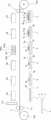
- FIG. 3 is a schematic configuration diagram of a thin film semiconductor manufacturing apparatus
- FIG. 4 is a plan view of a roll-shaped film substrate
- FIG. 5 is a schematic configuration diagram of a sputtering apparatus.
- barrier layers 3 and 4 are formed on both surfaces of the plastic substrate 2 of FIG.
- the thin film semiconductor manufacturing apparatus 100 includes roll winding mechanisms 110a and 110b, a sending mechanism 111, a winding mechanism 112, and an alignment mechanism 113, and the roll-shaped film substrate P is sent from the roll winding mechanism 110a.
- the thin film semiconductor device 1 is manufactured on the roll-shaped film substrate P sent out by the positioning mechanism 113 and sent out by the positioning mechanism 113, wound up by the winding mechanism 112, and mounted on the roll winding mechanism 110b.
- the roll-shaped film substrate P is sent out by detecting the alignment pattern A formed on the roll-shaped film substrate P by the alignment mechanism 113 and controlling the delivery mechanism 111 at a predetermined position. Align so that it stops.
- the sheet-like substrate bonding apparatus 120 the gate electrode forming apparatus 130, the insulating layer forming apparatus 140, the semiconductor layer forming apparatus 150, A drain electrode forming device 160 and a layer indirect edge film forming device 170 are arranged in this order.
- a sheet-like plastic substrate 60 is attached to the upper surface of the barrier layer 3 formed on the plastic substrate 2 via the adhesive layer 5 instead of the glass substrate.
- the gate electrode of the metal layer 9c is formed on the plastic substrate 60 by plating or sputtering, and in the insulating layer forming apparatus 140, the insulating layer 8a is formed by transfer or the like, and the semiconductor layer forming apparatus 150 is formed. Then, the semiconductor layer 7 is formed on the insulating layer 8a by a sputtering apparatus, and the source / drain electrode forming apparatus 160 forms the source electrode of the metal layer 9a and the drain electrode of the metal layer 9b by plating or sputtering, Furthermore, in the layer indirect edge film forming apparatus 170, the layer indirect edge film 8b is formed by transfer or the like, and the thin film semiconductor device 1 in FIG. 1 is manufactured.
- a thin film semiconductor manufacturing method is implemented by the thin film semiconductor manufacturing apparatus 100.
- the sputtering apparatus 150a holds the metal target 150a2 inside the vacuum chamber 150a1, and the atmosphere gas containing a nonmetallic element is supplied to the vacuum chamber 150a1.
- a high voltage is applied to the metal target 150a2
- atoms on its surface are repelled, and an atmosphere gas containing a nonmetallic element introduced into the vacuum chamber 150a1 is reacted with the repelled metal.
- the semiconductor layer 7 is formed on the roll film substrate P.
- the sputtering apparatus of this embodiment can be configured as shown in FIG. 5, and this sputtering apparatus 21 includes roll winding mechanisms 22 a and 22 b, a feeding mechanism 23, a winding mechanism 24, and an alignment mechanism 25. And a metal target 26a, 26b, and a vacuum chamber 27 that holds all these mechanisms inside.
- This vacuum chamber 27 has opening / closing doors 27a, 27b on the roll winding mechanisms 22a, 22b side, opens / closes the opening / closing door 27a, sets a roll-shaped film substrate P, opens / closes the opening / closing door 27b, and the semiconductor layer 7 is opened. The provided roll-shaped film substrate P is taken out.
- the roll-shaped film substrate P has barrier layers 3 and 4 formed on both surfaces of the plastic substrate 2 in FIG. 1, and the upper surface of the barrier layer 3 formed on the plastic substrate 2 is attached to the glass substrate via the adhesive layer 5.
- a sheet-like plastic substrate 60 is provided to form a roll, and has an alignment pattern A as shown in FIG.
- the roll winding mechanism 22a mounts the roll-shaped film substrate P on the rotation shaft 22a1, the rotation shaft 22a1 rotates by feeding the roll-shaped film substrate P, and the roll winding mechanism 22b causes the roll-shaped film substrate P to rotate on the rotation shaft 22b1.
- the rotating shaft 22b1 is rotated by winding the roll-shaped film substrate P.
- the delivery mechanism 23 has a pair of delivery rollers 23a, and feeds the roll-shaped film substrate P from one end along the longitudinal direction by the rotation of the pair of delivery rollers 23a.
- the winding mechanism 24 has a pair of winding rollers 24b and winds the roll-shaped film substrate P from one end along the longitudinal direction by the rotation of the pair of winding rollers 24b.
- the alignment mechanism 25 includes a detection sensor 25a, a control device 25b, and a roller drive device 25c.
- the detection sensor 25a detects the alignment pattern A of the roll film substrate P, and sends this detection information to the control device 25b.
- the control device 25b controls the feeding mechanism 23 and the winding mechanism 24 through the roller driving device 25c, and performs planar alignment of the roll-shaped film substrate P.
- the inside of the vacuum chamber 27 is in a vacuum state by being driven by a vacuum pump 28, and a gas introduction mechanism 29 is provided in the vacuum chamber 27. To introduce.
- the metal targets 26 a and 26 b face the semiconductor forming surface of the roll film substrate P and are arranged at linear positions along the length of the roll film substrate P.
- the metal target 26a is a metal element target, and the metal target 26ba is a semi-metal element target.
- the sputtering apparatus 21 uses metal mixtures 26a and 26b as a single target, which is a mixture of a plurality of elements including at least one of a nonmetallic element, a metallic element, and a semimetallic element, but the metallic target 26a. , 26b is a very good target.
- the sputtering apparatus 21 introduces the atmospheric gas containing the nonmetallic element into the vacuum chamber 27 by the gas introduction mechanism 29, and the metal element or metalloid element of the metal targets 26 a and 26 b or these elements into the vacuum chamber 27.
- a high voltage is applied to the metal targets 26 a and 26 b through the electrodes by arranging a plurality of metal targets containing a mixture of the above, atoms on the surface of the metal target are repelled and an atmospheric gas containing a nonmetallic element introduced into the vacuum chamber 27 Then, the semiconductor layer 7 can be formed on the roll-shaped film substrate P by reacting with the repelled metal.
- the roll-shaped film substrate P is not heated or cooled, and is placed at room temperature (however, a high voltage is applied to the metal targets 26a and 26b and reaction with flying atoms is performed. Therefore, it is considered that there is a natural temperature rise of about several tens of degrees Celsius).
- the pressure in the vacuum chamber 27 during film formation is about 0.5 Pa, and the partial pressure of the atmospheric gas supplied from the gas introduction mechanism 29 is about 0.005 Pa.
- the film forming power when a high voltage is applied to the metal target is about 2 W / cm 2 .
- the semiconductor layer 7 can be formed by a low temperature process using the sputtering apparatus 150a or the sputtering apparatus 21 of FIG. 5, and a low process cost can be realized. Moreover, the semiconductor layer 7 can manufacture the thin film semiconductor device 1 that can realize a relatively high field effect mobility and has stable characteristics with respect to light and heat.
- the semiconductor layer 7 can manufacture the thin film semiconductor manufacturing apparatus 1 that can freely control the band gap and increase the field effect mobility.
- the sputtering apparatus 21 of FIG. 5 includes a vacuum chamber 27 that holds all the mechanisms therein, and can be wound from a roll state to a feed roll state during manufacturing, thereby realizing a low process cost.
- the sputtering apparatus 21 introduces an atmospheric gas containing a non-metallic element into the vacuum chamber 27, has a plurality of metal targets 26a and 26b containing a metal element, a semi-metal element, or a mixture thereof, and the metal targets 26a and 26b.
- the semiconductor layer 7 having a uniform property can be formed in the roll-shaped film substrate P by being arranged at linear positions along the length of the roll-shaped film substrate P.
- the sputtering apparatus 21 uses a mixture obtained by mixing a plurality of elements including at least one of a non-metallic element, a metallic element, and a semi-metallic element as a single target, and makes the properties of the semiconductor layer 7 more uniform. Sputtering process costs can be reduced.
- the present invention is particularly applicable to a thin film semiconductor device, a thin film semiconductor manufacturing apparatus and a thin film semiconductor manufacturing method, which are flexible displays using a plastic substrate, can be formed by a low temperature process, realizes a low process cost, and is relatively High field effect mobility can be realized, and it has stable characteristics against light and heat, and can be applied to a bending environment.
Landscapes
- Physics & Mathematics (AREA)
- Nonlinear Science (AREA)
- Engineering & Computer Science (AREA)
- Microelectronics & Electronic Packaging (AREA)
- Mathematical Physics (AREA)
- Chemical & Material Sciences (AREA)
- Crystallography & Structural Chemistry (AREA)
- General Physics & Mathematics (AREA)
- Optics & Photonics (AREA)
- Thin Film Transistor (AREA)
- Liquid Crystal (AREA)
Abstract
低温プロセスで形成可能であり、低プロセスコストを実現し、また比較的高い電界効果移動度を実現でき、かつ光、熱に対して安定な特性を有し、曲げ環境にも適用できる薄膜半導体装置を提供する。 薄膜半導体装置(1)は、プラスチック基板(2)と、プラスチック基板(2)上に形成されたバリア層(3)と、バリア層(3)上に形成された半導体層7とを有し、半導体層(7)は、非金属元素のN、O、半金属元素のB、Si、Ge、As、Sb、Te、Poのうち少なくともひとつ、および金属元素のAl、Zn、Ga、Cd、In、Sn、Hg、Tl、Pb、Biのうち少なくともひとつを含み、非金属元素が、少なくともOとNの混合物で、Oに対するNの比(N数密度/O数密度)が0乃至2である。
Description
この発明は、特にプラスチック基板を用いたフレキシブルディスプレイである薄膜半導体装置、薄膜半導体製造装置及び薄膜半導体製造方法に関するものである。
ディスプレイの画像駆動用薄膜半導体装置(TFT)は、その半導体層として従来からa-Siが用いられており、現在も一般に普及している。しかし、a-Si を半導体層として用いたTFTは、その電界効果移動度は非常に小さいため(~0.1cm2/Vs)、近年急速に需要が増している高精細動画対応などの高機能用途には性能限界に達しつつあった。
このため、a-Siに代わる半導体層として、a-Siにエキシマレーザなどを照射して多結晶化することでより高い電界効果移動度(~10 cm2/Vs)が得られるpoly-Siを半導体層として用いたTFTが開発された(特許文献1など)。
この技術は、一部用途で実用化されたが、結晶粒界がランダムに分布することでTFT性能の均一化が困難なことやレーザプロセスコストが甚大なことなどが課題となり十分な普及はされていない。
さらに、前記したいずれのSi系TFTも半導体層の成膜温度が比較的高温であるため、フレキシブルディスプレイなどに用いるプラスチック基板やロール状フィルム基板の耐熱温度を超えてしまい、基板フレキシブル化への対応が困難であるという問題もあった。
これらに代わる新材料として、InGaZnOx系酸化物半導体が検討されている。このInGaZnOx系酸化物半導体は、スパッタなどの非真空・低温プロセスで成膜できるため、フレキシブル基板上にも形成可能であり、プロセスも低コストである。この酸化物半導体は、低温プロセス成膜後そのままの状態では未だ性能不十分で、成膜後のアニールによる焼き締めを行うことで十分な性能を引き出すことができる。焼き締めは、炉アニールの場合は300℃程度が必要なのでフレキシブル基板の(耐熱温度こそ超えないものの)熱膨張変形などの問題を起こしてしまう。そこでレーザーアニールなどの手法(poly-Si形成時より低エネルギーで良いためコスト上昇要因になりにくい)を併用することにより、低温のまま十分な焼き締めを行うことが考えられている。いずれの手法を用いても、この酸化物半導体はアモルファス状態が保たれるので、上述のpoly-Siのような粒界によるばらつき懸念がないこと、電界効果移動度(~10cm2/Vs)が比較的高く高精細動画対応にも可能なことなど、Siには無い多くの利点を持っている。
しかし、酸化物半導体は熱、光に対する安定性に課題があることが明らかとなってきた。外光(特に波長500nm以下の近紫外領域の光)が入射するとTFTのオフ電流が増大(波長370nmではオフ電流が約2桁増大)し、それに伴いTFTの閾値が5Vも変動する。ディスプレイはバックライトや外光などがTFTに入射しやすい構造のため、このような特性変動を起こすことは回路動作上非常に大きな問題となり得る。
このような外光への信頼性を増すためには、TFTの上下に金属(配線と共通化されている場合もある)からなる遮光層を設けることが行われるが、遮光層を避けて入射する迷光を完全に遮断することは困難なため完全な対策とはならない。
さらに、酸化物半導体は熱に対しても敏感で、上述したように成膜後のアニールにより焼き締めを行ったとしても、使用環境が100℃以上の温度になるとやはりオフ電流が増大し閾値が5V程度シフトする。このシフト量は使用環境温度が高いほど顕著で、200℃以上ではトランジスタがスイッチングできなくなるほどである。これは酸化物半導体中の酸素と他元素との結合状態が熱により変化することが原因と考えられている。この変化は可逆的で、使用環境が元に戻れば、TFT特性も数十分程度で元に戻るものの、ディスプレイ用途としては大きな課題であることに違いはない。
ディスプレイの通常使用環境ではこれほどの高温になることはないが、例えば車中など50~60℃で長時間放置されるような場合は、累積的な効果で特性変動する可能性が高い。このように酸化物半導体でも新たな課題が明らかとなりつつある。
この発明は、以上の点を考慮してなされたもので、低温プロセスで形成可能であり、低プロセスコストを実現し、また比較的高い電界効果移動度を実現でき、かつ光、熱に対して安定な特性を有し、曲げ環境にも適用できる薄膜半導体装置、薄膜半導体製造装置及び薄膜半導体製造方法を提案することを目的とする。
前記課題を解決し、かつ目的を達成するために、この発明は、以下のように構成した。
請求項1に記載の発明は、プラスチック基板と、
前記プラスチック基板上に形成されたバリア層と、
前記バリア層上に形成された半導体層と、
前記半導体層の上下いずれかの面に接して形成された絶縁層と、
前記絶縁層に接して形成された金属層と、
を有し、
前記半導体層をチャネル、前記金属層をソース電極、ドレイン電極、およびゲート電極、前記絶縁層をゲート絶縁膜として用い、
前記半導体層は、非金属元素の窒素(N)、酸素(O)のうち少なくともひとつ、半金属元素のホウ素(B)、シリコン(Si)、ゲルマニウム(Ge)、ヒ素(As)、アンチモン(Sb)、テルル(Te)、ポロニウム(Po)のうち少なくともひとつ、および金属元素のアルミニウム(Al)、亜鉛(Zn)、ガリウム(Ga)、カドニウム(Cd)、インジウム(In)、錫(Sn)、水銀(Hg)、タリウム(Tl)、テルビウム(Pb)、ビスマス(Bi)のうち少なくともひとつを含み、
前記非金属元素が、少なくとも酸素(O)と窒素(N)の混合物で、酸素(O)に対する窒素(N)の比(N数密度/O数密度)が0乃至2であることを特徴とする薄膜半導体装置である。
前記プラスチック基板上に形成されたバリア層と、
前記バリア層上に形成された半導体層と、
前記半導体層の上下いずれかの面に接して形成された絶縁層と、
前記絶縁層に接して形成された金属層と、
を有し、
前記半導体層をチャネル、前記金属層をソース電極、ドレイン電極、およびゲート電極、前記絶縁層をゲート絶縁膜として用い、
前記半導体層は、非金属元素の窒素(N)、酸素(O)のうち少なくともひとつ、半金属元素のホウ素(B)、シリコン(Si)、ゲルマニウム(Ge)、ヒ素(As)、アンチモン(Sb)、テルル(Te)、ポロニウム(Po)のうち少なくともひとつ、および金属元素のアルミニウム(Al)、亜鉛(Zn)、ガリウム(Ga)、カドニウム(Cd)、インジウム(In)、錫(Sn)、水銀(Hg)、タリウム(Tl)、テルビウム(Pb)、ビスマス(Bi)のうち少なくともひとつを含み、
前記非金属元素が、少なくとも酸素(O)と窒素(N)の混合物で、酸素(O)に対する窒素(N)の比(N数密度/O数密度)が0乃至2であることを特徴とする薄膜半導体装置である。
請求項2に記載の発明は、前記半金属元素が、少なくともシリコン(Si)とゲルマニウム(Ge)の混合物Si1-xGex(xはSiとGeの混合比でx=0乃至1が成り立つ)で、前記混合物(Si1-xGex)に対する窒素(N)の比(N数密度/Si1-xGex数密度)が1乃至2であることを特徴とする請求項1に記載の薄膜半導体装置である。
請求項3に記載の発明は、前記プラスチック基板が、少なくともロール状フィルム基板であることを特徴とする請求項1または請求項2に記載の薄膜半導体装置である。
請求項4に記載の発明は、前記半導体層は、アモルファスであることを特徴とする請求項1乃至請求項3のいずれか1項に記載の薄膜半導体装置である。
請求項5に記載の発明は、前記半導体層のバンドギャップは、1eV乃至5eVであることを特徴とする請求項1乃至請求項4のいずれか1項に記載の薄膜半導体装置である。
請求項6に記載の発明は、前記半導体層の主キャリアは、電子で、キャリア濃度は300Kの熱平衡状態において1×10E16乃至1×10E21(m-3)、電界効果移動度は0.1乃至50(cm2/Vs)であることを特徴とする請求項1乃至請求項4のいずれか1項に記載の薄膜半導体装置である。
請求項7に記載の発明は、前記半導体層が、液晶表示装置を駆動する回路を構成することを特徴とする請求項1乃至請求項6のいずれか1項に記載の薄膜半導体装置である。
請求項8に記載の発明は、前記ロール状フィルム基板と、
前記ロール状フィルム基板上に形成されたバリア層と、
前記バリア層上に形成された半導体層と、
前記半導体層の上下いずれかの面に接して形成された絶縁層と、
前記絶縁層に接して形成された金属層と、
を有し、
前記半導体層をチャネル、前記金属層をソース電極、ドレイン電極、およびゲート電極、前記絶縁層をゲート絶縁膜として用い、
前記半導体層は、非金属元素の窒素(N)、酸素(O)のうち少なくともひとつ、半金属元素のホウ素(B)、シリコン(Si)、ゲルマニウム(Ge)、ヒ素(As)、アンチモン(Sb)、テルル(Te)、ポロニウム(Po)のうち少なくともひとつ、および金属元素のアルミニウム(Al)、亜鉛(Zn)、ガリウム(Ga)、カドニウム(Cd)、インジウム(In)、錫(Sn)、水銀(Hg)、タリウム(Tl)、テルビウム(Pb)、ビスマス(Bi)のうち少なくともひとつを含み、
前記非金属元素が、少なくとも酸素(O)と窒素(N)の混合物で酸素(O)に対する窒素(N)の比(N数密度/O数密度)が0乃至2である前記半導体層をスパッタ装置により形成する薄膜半導体製造装置である。
前記ロール状フィルム基板上に形成されたバリア層と、
前記バリア層上に形成された半導体層と、
前記半導体層の上下いずれかの面に接して形成された絶縁層と、
前記絶縁層に接して形成された金属層と、
を有し、
前記半導体層をチャネル、前記金属層をソース電極、ドレイン電極、およびゲート電極、前記絶縁層をゲート絶縁膜として用い、
前記半導体層は、非金属元素の窒素(N)、酸素(O)のうち少なくともひとつ、半金属元素のホウ素(B)、シリコン(Si)、ゲルマニウム(Ge)、ヒ素(As)、アンチモン(Sb)、テルル(Te)、ポロニウム(Po)のうち少なくともひとつ、および金属元素のアルミニウム(Al)、亜鉛(Zn)、ガリウム(Ga)、カドニウム(Cd)、インジウム(In)、錫(Sn)、水銀(Hg)、タリウム(Tl)、テルビウム(Pb)、ビスマス(Bi)のうち少なくともひとつを含み、
前記非金属元素が、少なくとも酸素(O)と窒素(N)の混合物で酸素(O)に対する窒素(N)の比(N数密度/O数密度)が0乃至2である前記半導体層をスパッタ装置により形成する薄膜半導体製造装置である。
請求項9に記載の発明は、前記半金属元素が、少なくともシリコン(Si)とゲルマニウム(Ge)の混合物Si1-xGex(xはSiとGeの混合比でx=0乃至1が成り立つ)で、前記混合物(Si1-xGex)に対する窒素(N)の比(N数密度/Si1-xGex数密度)が1乃至2であることを特徴とする請求項8に記載の薄膜半導体製造装置である。
請求項10に記載の発明は、前記スパッタ装置は、
前記ロール状フィルム基板を装着するロール巻機構と、
前記ロール状フィルム基板を長尺方向に沿って一方の端部から送り出す送出機構と、
送り出された前記ロール状フィルム基板を巻き取る巻取機構と、
位置合わせパターンを有する前記ロール状フィルム基板に対し、前記ロール状フィルム基板の平面位置合わせを行う位置合わせ機構と、
前記ロール状フィルム基板の半導体形成面に対面する金属ターゲットと、
を有し、
前記全ての機構を内部に保持する真空チャンバを備えたことを特徴とする請求項8また請求項9に記載の薄膜半導体製造装置である。
前記ロール状フィルム基板を装着するロール巻機構と、
前記ロール状フィルム基板を長尺方向に沿って一方の端部から送り出す送出機構と、
送り出された前記ロール状フィルム基板を巻き取る巻取機構と、
位置合わせパターンを有する前記ロール状フィルム基板に対し、前記ロール状フィルム基板の平面位置合わせを行う位置合わせ機構と、
前記ロール状フィルム基板の半導体形成面に対面する金属ターゲットと、
を有し、
前記全ての機構を内部に保持する真空チャンバを備えたことを特徴とする請求項8また請求項9に記載の薄膜半導体製造装置である。
請求項11に記載の発明は、前記スパッタ装置は、
前記非金属元素を含む雰囲気ガスを真空チャンバ内に導入するガス導入機構と、
前記金属元素または前記半金属元素またはこれらの混合物を含む金属ターゲットと、を複数有し、
前記金属ターゲットが、前記ロール状フィルム基板の長尺に沿った直線状の位置に配列されていることを特徴とする請求項8または請求項9に記載の薄膜半導体製造装置である。
前記非金属元素を含む雰囲気ガスを真空チャンバ内に導入するガス導入機構と、
前記金属元素または前記半金属元素またはこれらの混合物を含む金属ターゲットと、を複数有し、
前記金属ターゲットが、前記ロール状フィルム基板の長尺に沿った直線状の位置に配列されていることを特徴とする請求項8または請求項9に記載の薄膜半導体製造装置である。
請求項12に記載の発明は、前記スパッタ装置は、
前記非金属元素、前記金属元素、前記半金属元素それぞれ少なくともひとつを含む複数の元素を混ぜ合わせた混合物を、単一のターゲットとして用いたことを特徴とする請求項8乃至請求項11のいずれか1項に記載の薄膜半導体製造装置である。
前記非金属元素、前記金属元素、前記半金属元素それぞれ少なくともひとつを含む複数の元素を混ぜ合わせた混合物を、単一のターゲットとして用いたことを特徴とする請求項8乃至請求項11のいずれか1項に記載の薄膜半導体製造装置である。
請求項13に記載の発明は、請求項8乃至請求項12のいずれか1項に記載の薄膜半導体製造装置を用い、
薄膜半導体装置を製造することを特徴とする薄膜半導体製造方法である。
薄膜半導体装置を製造することを特徴とする薄膜半導体製造方法である。
前記構成により、この発明は、以下のような効果を有する。
請求項1に記載の発明では、薄膜半導体装置の半導体層をチャネル、金属層をソース、ドレイン、およびゲート、絶縁層をゲート絶縁膜として用い、半導体層は、非金属元素の窒素(N)、酸素(O)のうち少なくともひとつ、半金属元素のホウ素(B)、シリコン(Si)、ゲルマニウム(Ge)、ヒ素(As)、アンチモン(Sb)、テルル(Te)、ポロニウム(Po)のうち少なくともひとつ、および金属元素のアルミニウム(Al)、亜鉛(Zn)、ガリウム(Ga)、カドニウム(Cd)、インジウム(In)、錫(Sn)、水銀(Hg)、タリウム(Tl)、テルビウム(Pb)、ビスマス(Bi)のうち少なくともひとつを含み、非金属元素が、少なくとも酸素(O)と窒素(N)の混合物で、酸素(O)に対する窒素(N)の比(N数密度/O数密度)が0乃至2であることで、半導体層への窒素(N)の導入により比較的高い電界効果移動度を実現できる。また、半導体層への窒素(N)の導入によりバンドギャップを広げることで、光、熱による特性変動を抑制することができる。また、半導体層への窒素(N)の導入により弾性定数(ヤング率)を増加させ、プラスチック基板やロール状フィルム基板上での構造的強度を向上させ、曲げ環境にも適用できる。また、半導体層は、スパッタリングの低温プロセスで形成可能であり、低プロセスコストを実現できる。
請求項2に記載の発明では、半金属元素が、少なくともシリコン(Si)とゲルマニウム(Ge)の混合物Si1-xGex(xはSiとGeの混合比でx=0乃至1が成り立つ)で、前記混合物(Si1-xGex)に対する窒素(N)の比(N数密度/Si1-xGex数密度)が1乃至2であり、半金属元素のシリコン(Si)にゲルマニウム(Ge)を導入することによりバンドギャップを小さくすることができ、これと請求項1の窒素(N)の導入によるバンドギャップ増大とを組み合わせて、自在にバンドギャップを制御でき、また電界効果移動度を増大させることができる。
請求項3に記載の発明では、プラスチック基板が、少なくともロール状フィルム基板であり、製造時にロール状態から送り出しロール状態に巻き取り、低プロセスコストを実現し、低価格のディスプレイを提供することができる。
請求項4に記載の発明では、半導体層は、アモルファスであり、粒界がないことで、特性の均一性を増加させ、かつプラスチック基板やロール状フィルム基板上に形成された場合の曲げ強度を向上させることができる。
請求項5に記載の発明では、半導体層のバンドギャップは、半導体層への窒素(N)の導入により広げることができるが、1eV乃至5eVであることで、可視から近紫外領域の外光入射による特性変動を抑制することができる。
請求項6に記載の発明では、半導体層の主キャリアは、電子で、キャリア濃度は300Kの熱平衡状態において1×10E16乃至1×10E21(m-3)、電界効果移動度は0.1乃至50(cm2/Vs)であり、より高い電界効果移動度が得られることで、高精細の動画まで対応できる。
請求項7に記載の発明では、半導体層が、液晶表示装置を駆動する回路を構成し、
アクティブマトリクス型液晶表示装置に対応できる。
アクティブマトリクス型液晶表示装置に対応できる。
請求項8に記載の発明では、半導体層をスパッタ方式により形成することで、低温プロセスで形成可能であり、低プロセスコストを実現し、また比較的高い移動度を実現でき、かつ光、熱に対して安定な特性を有する薄膜半導体装置を製造することができる。
請求項9に記載の発明では、自在にバンドギャップを制御でき、また電界効果移動度を増大させることができる薄膜半導体製造装置を製造することができる。
請求項10に記載の発明では、スパッタ装置は、全ての機構を内部に保持する真空チャンバを備え、製造時にロール状態から送り出しロール状態に巻き取るロールツーロール法を用いて低プロセスコストを実現することができる。
請求項11に記載の発明では、スパッタ装置は、非金属元素を含む雰囲気ガスを真空チャンバ内に導入し、金属元素または半金属元素またはこれらの混合物を含む金属ターゲットを複数有し、金属ターゲットが、ロール状フィルム基板の長尺に沿った直線状の位置に配列され、ロール状フィルム基板内に均一な性質の半導体層を形成できる。
請求項12に記載の発明では、スパッタ装置は、非金属元素、金属元素、半金属元素それぞれ少なくともひとつを含む複数の元素を混ぜ合わせた混合物を、単一のターゲットとして用い、半導体層の性質をさらに均一にするとともにスパッタプロセスコストを低減できる。
請求項13に記載の発明では、請求項8乃至請求項12のいずれか1項に記載の薄膜半導体製造装置を用い、薄膜半導体装置を製造する。
以下、この発明の薄膜半導体装置、薄膜半導体製造装置及び薄膜半導体製造方法の実施の形態について説明する。この実施の形態は好ましい形態を示すものであるが、この発明はこれに限定されない。
[薄膜半導体装置]
まず、この発明の薄膜半導体装置について説明する。図1は薄膜半導体装置の構成を説明する断面図である。
まず、この発明の薄膜半導体装置について説明する。図1は薄膜半導体装置の構成を説明する断面図である。
この実施の形態の薄膜半導体装置1は、プラスチック基板2を有し、このプラスチック基板2の両面にバリア層3,4が形成されている。プラスチック基板2上に形成されたバリア層3の上面には、接着層5を介してガラス基板6が設けられ、このガラス基板6の上面に半導体層7が形成されている。ガラス基板6は、半導体層7を形成するための土台として、ある程度の厚さ(0.5mm程度)を持っていた元状態から、半導体層7形成後にエッチングなどの処理で削って薄型化(0.1mm以下)したものであり、接着層5を介してプラスチック基板2と半導体層7が接合された後は不要となる。このため、場合によりガラス基板6を完全にエッチング除去しても良い。
このようにして半導体層7がバリア層3上に形成され、この半導体層7の下面がガラス基板6の上面に形成した絶縁層8aと接して形成され、上面が層間絶縁膜8bと接して形成されている。絶縁層8a下面に接して金属層9cが形成されている。また、半導体層7上面に接して金属層9a、9bが形成されている。半導体層7をチャネル、金属層9aをソース電極、金属層9bをドレイン電極、および金属層9cをゲート電極、絶縁層8aをゲート絶縁膜として用いている。図1では上から、金属層9aおよび9b、半導体層7、絶縁層8a、金属層9cの順となっている(ボトムゲート構造)が、場合により上下を逆にして、上から金属層9c、絶縁層8a、半導体層7、金属層9aおよび9b(トップゲート構造)としても良いことは言うまでもない。
半導体層7は、非金属元素の窒素(N)、酸素(O)のうち少なくともひとつ、半金属元素のホウ素(B)、シリコン(Si)、ゲルマニウム(Ge)、ヒ素(As)、アンチモン(Sb)、テルル(Te)、ポロニウム(Po)のうち少なくともひとつ、および金属元素のアルミニウム(Al)、亜鉛(Zn)、ガリウム(Ga)、カドニウム(Cd)、インジウム(In)、錫(Sn)、水銀(Hg)、タリウム(Tl)、テルビウム(Pb)、ビスマス(Bi)のうち少なくともひとつを含み、非金属元素が、少なくとも酸素(O)と窒素(N)の混合物で酸素(O)に対する窒素(N)の比(N数密度/O数密度)が0乃至2である。
半導体層7は、金属原料(In2O3, SnO2)と絶縁体原料(Si3N4)の組み合わせから作製する。金属原料は窒化物を用いようとしてもそれ自体が初めから絶縁体なので、他の絶縁体原料といくら混ぜても半導体は形成できない。このため、金属原料はそれ自体が金属である酸化物を用いる。これに対し、絶縁体原料に窒化物を用いると、両者を混ぜて作製される半導体は酸素(O)と窒素(N)の両方を含む酸窒化物の混合物となる。混合の様子を次の式で表す。正負の価数が釣り合う条件で混合比x、yを決めることができる。

主たる金属原料In2O3の混合比x、絶縁体材料Si3N4の混合比yとすると、価数釣り合いから、従たる金属原料SnO2の混合比は6-xとなる。金属原料と絶縁体原料の比x:yは、原料それぞれのバンドギャップと、混合後に形成される半導体のバンドギャップによって決まり、例えばxの範囲としてはx=0~6(典型値5)、yの範囲としてはy=0~6(典型値3)が望ましい。
従って、O:Nの数量比は、
O=12~18 (典型値17)
N=0~24(典型値12)となる。
従って、O:N=1:0~2
酸素1に対する窒素の数密度比、すなわち酸素(O)に対する窒素(N)の比(N数密度/O数密度)は0乃至2である。
従って、O:Nの数量比は、
O=12~18 (典型値17)
N=0~24(典型値12)となる。
従って、O:N=1:0~2
酸素1に対する窒素の数密度比、すなわち酸素(O)に対する窒素(N)の比(N数密度/O数密度)は0乃至2である。
また、半金属元素が、少なくともシリコン(Si)とゲルマニウム(Ge)の混合物Si1-xGex(xはSiとGeの混合比でx=0乃至1が成り立つ)で、混合物(Si1-xGex)に対する窒素(N)の比(N数密度/Si1-xGex数密度)が1乃至2である。
Si:Geの組成比は、
Si、Ge間の組成変化は前記バランスに影響しないので、
Siに対するGeの組成比は、Si1-xGexにおいてx=0~1である。
Si:Geの組成比は、
Si、Ge間の組成変化は前記バランスに影響しないので、
Siに対するGeの組成比は、Si1-xGexにおいてx=0~1である。
SiGeに対する窒素の数量比は、
(Si1-xGex)3yに対しN4yより常に1:1.33である。
(Si1-xGex)3yに対しN4yより常に1:1.33である。
この実施の形態では、半導体層7は、非金属元素の窒素(N)、酸素(O)のうち少なくともひとつ、半金属元素のホウ素(B)、シリコン(Si)、ゲルマニウム(Ge)、ヒ素(As)、アンチモン(Sb)、テルル(Te)、ポロニウム(Po)のうち少なくともひとつ、および金属元素のアルミニウム(Al)、亜鉛(Zn)、ガリウム(Ga)、カドニウム(Cd)、インジウム(In)、錫(Sn)、水銀(Hg)、タリウム(Tl)、テルビウム(Pb)、ビスマス(Bi)のうち少なくともひとつを含むことで、安価で容易に得ることができる半金属元素、金属元素を用いている。
上述の半金属元素、金属元素は、いずれもそれぞれの単体で半金属、金属として振る舞うものである。元素にはこの他にもアルカリ金属、遷移元素などがあり、それらの混合物まで考えると候補は無数に考えられるが、単体でわかりやすい性質を持つこと、入手しやすさ、原料費、プロセス取り扱いなどに優れている点を考慮すると、候補原料は事実上これらに限定される。
また、室温でのスパッタプロセスで形成できる酸化物半導体をベースし、これに酸素(O)のみでなく窒素(N)を組み合わせた酸窒化物半導体とする。
非金属元素が、少なくとも酸素(O)と窒素(N)の混合物で、酸素(O)に対する窒素(N)の比(N数密度/O数密度)が0乃至2であることで、半導体層7への窒素(N)の導入により比較的高い電界効果移動度を実現できる。また、半導体層7への窒素(N)の導入によりバンドギャップを広げることで、光、熱による特性変動を抑制することができる。また、半導体層7への窒素(N)の導入により弾性定数(ヤング率)を増加させ、プラスチック基板やロール状フィルム基板上での構造的強度を向上させ、低温プロセスで形成可能であり、低プロセスコストを実現できる。
酸素(O)に対する窒素(N)の比(N数密度/O数密度)が0乃至2の範囲となるのは、上記「酸素(O)に対する窒素(N)の比(N数密度/O数密度)は0乃至2」について述べたように、バンドギャップと価数釣り合いから決まる。仮にこの値が0(窒素が全く存在しない)となった場合、酸素の量によっては、半導体のバンドギャップが小さすぎて金属的となり、薄膜半導体装置1が常時オン状態となってしまう。逆にこの値が2を超える(酸素不足、窒素過剰)場合、半導体のバンドギャップが大きすぎて絶縁体的となり、薄膜半導体装置1が常時オフ状態となってしまう。いずれの場合もTFT特性として問題が起きる。
また、半金属元素が、少なくともシリコン(Si)とゲルマニウム(Ge)の混合物Si1-xGex(xはSiとGeの混合比でx=0乃至1が成り立つ)で、混合物(Si1-xGex)に対する窒素(N)の比(N数密度/Si1-xGex数密度)が1乃至2であり、半金属元素のシリコン(Si)にゲルマニウム(Ge)を導入することによりバンドギャップを小さくすることができ、これと窒素(N)の導入によるバンドギャップ増大とを組み合わせて、自在にバンドギャップを制御でき、また電界効果移動度を増大させることができる。
混合物(Si1-xGex)に対する窒素(N)の比(N数密度/Si1-xGex数密度)が1乃至2であることは、上記「混合の様子を表す式」から導かれる。すなわちSiの混合比が3yの時、Nの混合比は4yであるため、その比は1.33となり1乃至2の範囲に収まる。ところが半導体形成過程ではスパッタ工程中のガス流量、密度などにより窒素の過不足が発生し、1.33を中心としたある範囲のばらつきが起こる。多少のばらつきの範囲であれば薄膜半導体装置として動作に問題が起こらないが、この値が1未満の極端な窒素不足あるいは2以上の極端な窒素過剰の場合には半導体が形成されず、それぞれ金属、絶縁体となってしまうため相応しくない。
半導体層7のバンドギャップは、半導体層7への窒素(N)の導入により広げることができるが、バンドギャップが、1eV乃至5eVであることで、可視から近紫外領域の外光入射による特性変動を抑制することができる。
バンドギャップが1eV以下の場合、価電子帯のキャリアが小さなエネルギーで容易に伝導帯に励起されるため、TFTのオフ電流が増加して消費電力が増し、極端な場合は常時オン状態となりスイッチングすらできなくなってしまう。この小さなエネルギー源には光のみでなく熱もなり得るため、温度に対してもTFT動作が不安定になる。一方、バンドギャップが5eV以上になると、価電子帯のキャリアが大きなエネルギーによっても伝導帯に励起されなくなるため、TFTのオン電流が減少して移動度を確保できなくなり、極端な場合は常時オフ状態となりスイッチングできなくなってしまう。このような場合は、元々特性の良い酸窒化物半導体を使うメリットがなくなる。
また、半導体層7の主キャリアは、電子で、キャリア濃度は300Kの熱平衡状態において1×10E16乃至1×10E21(m-3)、電界効果移動度は0.1乃至50(cm2/Vs)であり、高精細の動画まで対応できる。
電界効果移動度が0.1未満の場合、アモルファスシリコン程度以下となってしまうので、この実施の形態の酸窒化物半導体を用いる利点がなくなってしまう。また、電界効果移動度上限50は、この実施の形態の酸窒化物半導体が最適な条件で形成された場合の性能限界に相当する。
この実施の形態の薄膜半導体装置1は、ディスプレイを駆動する回路に用いられ、薄膜半導体装置1の半導体層7が、液晶表示装置を駆動する回路を構成し、アクティブマトリクス型液晶表示装置に対応でき、さらにアクティブマトリックス型有機EL表示装置などに対応できる。
図2はロール状フィルム基板上に形成された薄膜半導体装置を示す図である。
ロール状フィルム基板P上には、所定位置にディスプレイパネルDが複数個形成され、この実施の形態ではディスプレイパネルDが4個ずつ所定間隔で長尺方向に沿って形成されている。このディスプレイパネルDは、拡大して示すように、画素Gと、ゲート線L1と、データ線L2と、薄膜半導体装置1を有している。
図1のプラスチック基板2は、少なくともロール状フィルム基板Pとし、ガラス基板6もフィルム基板とすることで、製造時にロール状態から送り出しロール状態に巻き取るロールツーロール法を用いて低プロセスコストを実現し、曲げ環境にも適用できるフレキシブルディスプレイを製造することができる。
また、半導体層7は、アモルファスであり、粒界がないことで、特性の均一性を増加させ、かつプラスチック基板やロール状フィルム基板上に形成された場合の曲げ強度を向上させることができる。
[薄膜半導体製造装置及び薄膜半導体製造方法]
次に、薄膜半導体製造装置及び薄膜半導体製造方法について説明する。図3は薄膜半導体製造装置の概略構成図、図4はロール状フィルム基板の平面図、図5はスパッタ装置の概略構成図である。
次に、薄膜半導体製造装置及び薄膜半導体製造方法について説明する。図3は薄膜半導体製造装置の概略構成図、図4はロール状フィルム基板の平面図、図5はスパッタ装置の概略構成図である。
図3において、薄膜半導体製造装置100は、図1の薄膜半導体装置1を製造するから薄膜半導体装置1の説明は同じ符号を付して省略する。ロール状フィルム基板Pは、図1のプラスチック基板2の両面にバリア層3,4が形成されている。
この薄膜半導体製造装置100は、ロール巻機構110a,110bと、送出機構111と、巻取機構112と、位置合わせ機構113とを有し、ロール巻機構110aからロール状フィルム基板Pを送出機構111によって送り出し、位置合わせ機構113によって位置決めして送り出されたロール状フィルム基板P上に薄膜半導体装置1を製造して巻取機構112に巻き取り、ロール巻機構110bに装着する。
このロール状フィルム基板Pの送り出しは、位置合わせ機構113によって、図4に示すように、ロール状フィルム基板Pに形成された位置合わせパターンAを検出し、送出機構111を制御して所定位置で停止するように位置合わせを行う。
このロール状フィルム基板Pが搬送される直線状の位置に沿って、シート状基板貼合装置120と、ゲート電極形成装置130と、絶縁層形成装置140と、半導体層形成装置150と、ソース・ドレイン電極形成装置160と、層間接縁膜形成装置170が順に配置されている。
シート状基板貼合装置120では、プラスチック基板2上に形成されたバリア層3の上面には、接着層5を介してガラス基板に代えてシート状プラスチック基板60を貼り付ける。
ゲート電極形成装置130では、プラスチック基板60の上に金属層9cのゲート電極をメッキやスパッタリングなどで形成し、絶縁層形成装置140では、絶縁層8aを転写などで形成し、半導体層形成装置150では、スパッタ装置により絶縁層8aの上に半導体層7を形成し、ソース・ドレイン電極形成装置160では、金属層9aのソース電極と、金属層9bのドレイン電極をメッキやスパッタリングなどによって形成し、さらに層間接縁膜形成装置170では、層間接縁膜8bを転写などによって形成し、図1の薄膜半導体装置1を製造する。
この薄膜半導体製造装置100によって薄膜半導体製造方法が実施され、半導体層形成装置150では、スパッタ装置150aが真空チャンバ150a1の内部に金属ターゲット150a2を保持し、非金属元素を含む雰囲気ガスを真空チャンバ150a1内に導入する用に構成され、金属ターゲット150a2に高電圧をかけるとその表面の原子がはじき飛ばされ、真空チャンバ150a1内に導入された非金属元素を含む雰囲気ガスと、はじき飛ばされた金属と反応させることによって、ロール状フィルム基板Pに半導体層7を製膜する。
この実施の形態のスパッタ装置は、図5に示すように構成することができ、このスパッタ装置21は、ロール巻機構22a,22bと、送出機構23と、巻取機構24と、位置合わせ機構25と、金属ターゲット26a,26bと、を有し、これらの全ての機構を内部に保持する真空チャンバ27を備えている。この真空チャンバ27は、ロール巻機構22a,22b側に開閉扉27a,27bを有し、開閉扉27aを開閉してロール状フィルム基板Pをセットし、開閉扉27bを開閉して半導体層7が設けられたロール状フィルム基板Pを取り出す。
ロール状フィルム基板Pは、図1のプラスチック基板2の両面にバリア層3,4が形成され、プラスチック基板2上に形成されたバリア層3の上面には、接着層5を介してガラス基板に代えてシート状プラスチック基板60を設けてロール状にした構成であり、図4に示すように、位置合わせパターンAを有する。
ロール巻機構22aは、回転軸22a1にロール状フィルム基板Pを装着し、回転軸22a1はロール状フィルム基板Pの送り出しによって回転し、ロール巻機構22bは、回転軸22b1にロール状フィルム基板Pを装着し、回転軸22b1はロール状フィルム基板Pの巻き取りによって回転する。
送出機構23は、一対の送出ローラ23aを有し、この一対の送出ローラ23aの回転によってロール状フィルム基板Pを長尺方向に沿って一方の端部から送り出す。
巻取機構24は、一対の巻取ローラ24bを有し、この一対の巻取ローラ24bの回転によってロール状フィルム基板Pを長尺方向に沿って一方の端部から巻き取る。
位置合わせ機構25は、検出センサ25a、制御装置25b、ローラ駆動装置25cを有し、検出センサ25aによってロール状フィルム基板Pの位置合わせパターンAを検出し、この検出情報を制御装置25bに送り、制御装置25bはローラ駆動装置25cを介して送出機構23及び巻取機構24を制御し、ロール状フィルム基板Pの平面位置合わせを行う。
真空チャンバ27内は、真空ポンプ28に駆動によって真空状態であり、この真空チャンバ27には、ガス導入機構29が設けられ、このガス導入機構29は非金属元素を含む雰囲気ガスを真空チャンバ27内に導入する。
金属ターゲット26a,26bは、ロール状フィルム基板Pの半導体形成面に対面し、ロール状フィルム基板Pの長尺に沿った直線状の位置に配列されている。
金属ターゲット26aは、金属元素のターゲットであり、金属ターゲット26baは、半金属元素のターゲットである。
スパッタ装置21は、金属ターゲット26a,26bとし、非金属元素、金属元素、半金属元素それぞれ少なくともひとつを含む複数の元素を混ぜ合わせた混合物を、単一のターゲットとして用いているが、金属ターゲット26a,26bを一体のターゲットとてもよい。
このように、スパッタ装置21は、ガス導入機構29により、真空チャンバ27内に非金属元素を含む雰囲気ガスを導入し、真空チャンバ27内に金属ターゲット26a,26bの金属元素または半金属元素またはこれらの混合物を含む金属ターゲットを複数配置し、電極を介して金属ターゲット26a,26bに高電圧をかけると金属ターゲット表面の原子がはじき飛ばされ、真空チャンバ27内に導入された非金属元素を含む雰囲気ガスと、はじき飛ばされた金属と反応させることによって、ロール状フィルム基板Pに半導体層7を製膜することができる。
半導体層7を成膜する場合、ロール状フィルム基板Pは特に加熱や冷却されることはなく室温に置かれる(ただし、金属ターゲット26a、26bへの高電圧印加やはじき飛んでくる原子との反応により、数十℃程度の自然昇温はあると考えられる)。また、成膜時の真空チャンバ27内の圧力は約0.5Pa、ガス導入機構29から供給される雰囲気ガスの分圧は約0.005Paである。金属ターゲットへの高電圧印加の成膜パワーは約2W/cm2である。
この薄膜半導体製造装置100では、スパッタ装置150aまたは図5のスパッタ装置21を用い、低温プロセスで半導体層7を形成可能であり、低プロセスコストを実現することができる。また、半導体層7は、比較的高い電界効果移動度を実現でき、かつ光、熱に対して安定な特性を有する薄膜半導体装置1を製造することができる。
また、半導体層7は自在にバンドギャップを制御でき、また電界効果移動度を増大させることができる薄膜半導体製造装置1を製造することができる。
また、図5のスパッタ装置21は、全ての機構を内部に保持する真空チャンバ27を備え、製造時にロール状態から送り出しロール状態に巻き取り、低プロセスコストを実現することができる。
また、スパッタ装置21は、非金属元素を含む雰囲気ガスを真空チャンバ27内に導入し、金属元素または半金属元素またはこれらの混合物を含む金属ターゲット26a,26bを複数有し、金属ターゲット26a,26bが、ロール状フィルム基板Pの長尺に沿った直線状の位置に配列され、ロール状フィルム基板P内に均一な性質の半導体層7を形成できる。
また、スパッタ装置21は、非金属元素、金属元素、半金属元素それぞれ少なくともひとつを含む複数の元素を混ぜ合わせた混合物を、単一のターゲットとして用い、半導体層7の性質をさらに均一にするとともにスパッタプロセスコストを低減できる。
この発明は、特にプラスチック基板を用いたフレキシブルディスプレイである薄膜半導体装置、薄膜半導体製造装置及び薄膜半導体製造方法に適用可能で、低温プロセスで形成可能であり、低プロセスコストを実現し、また比較的高い電界効果移動度を実現でき、かつ光、熱に対して安定な特性を有し、曲げ環境にも適用できる。
1 薄膜半導体装置
2 プラスチック基板
3,4 バリア層
5 接着層
6 ガラス基板
7 半導体層
8a 絶縁層
9a,9b,9c 金属層
21,150a スパッタ装置
22a,22b ロール巻機構
23 送出機構
24 巻取機構
25 位置合わせ機構
26a,26b 金属ターゲット
27 真空チャンバ
29 ガス導入機構
P ロール状フィルム基板
2 プラスチック基板
3,4 バリア層
5 接着層
6 ガラス基板
7 半導体層
8a 絶縁層
9a,9b,9c 金属層
21,150a スパッタ装置
22a,22b ロール巻機構
23 送出機構
24 巻取機構
25 位置合わせ機構
26a,26b 金属ターゲット
27 真空チャンバ
29 ガス導入機構
P ロール状フィルム基板
Claims (13)
- プラスチック基板と、
前記プラスチック基板上に形成されたバリア層と、
前記バリア層上に形成された半導体層と、
前記半導体層の上下いずれかの面に接して形成された絶縁層と、
前記絶縁層に接して形成された金属層と、
を有し、
前記半導体層をチャネル、前記金属層をソース電極、ドレイン電極、およびゲート電極、前記絶縁層をゲート絶縁膜として用い、
前記半導体層は、非金属元素の窒素(N)、酸素(O)のうち少なくともひとつ、半金属元素のホウ素(B)、シリコン(Si)、ゲルマニウム(Ge)、ヒ素(As)、アンチモン(Sb)、テルル(Te)、ポロニウム(Po)のうち少なくともひとつ、および金属元素のアルミニウム(Al)、亜鉛(Zn)、ガリウム(Ga)、カドニウム(Cd)、インジウム(In)、錫(Sn)、水銀(Hg)、タリウム(Tl)、テルビウム(Pb)、ビスマス(Bi)のうち少なくともひとつを含み、
前記非金属元素が、少なくとも酸素(O)と窒素(N)の混合物で、酸素(O)に対する窒素(N)の比(N数密度/O数密度)が0乃至2であることを特徴とする薄膜半導体装置。 - 前記半金属元素が、少なくともシリコン(Si)とゲルマニウム(Ge)の混合物Si1-xGex(xはSiとGeの混合比でx=0乃至1が成り立つ)で、前記混合物(Si1-xGex)に対する窒素(N)の比(N数密度/Si1-xGex数密度)が1乃至2であることを特徴とする請求項1に記載の薄膜半導体装置。
- 前記プラスチック基板が、少なくともロール状フィルム基板であることを特徴とする請求項1または請求項2に記載の薄膜半導体装置。
- 前記半導体層は、アモルファスであることを特徴とする請求項1乃至請求項3のいずれか1項に記載の薄膜半導体装置。
- 前記半導体層のバンドギャップは、1eV乃至5eVであることを特徴とする請求項1乃至請求項4のいずれか1項に記載の薄膜半導体装置。
- 前記半導体層の主キャリアは、電子で、キャリア濃度は300Kの熱平衡状態において1×10E16乃至1×10E21(m-3)、電界効果移動度は0.1乃至50(cm2/Vs)であることを特徴とする請求項1乃至請求項4のいずれか1項に記載の薄膜半導体装置。
- 前記半導体層が、液晶表示装置を駆動する回路を構成することを特徴とする請求項1乃至請求項6のいずれか1項に記載の薄膜半導体装置。
- 前記ロール状フィルム基板と、
前記ロール状フィルム基板上に形成されたバリア層と、
前記バリア層上に形成された半導体層と、
前記半導体層の上下いずれかの面に接して形成された絶縁層と、
前記絶縁層に接して形成された金属層と、
を有し、
前記半導体層をチャネル、前記金属層をソース電極、ドレイン電極、およびゲート電極、前記絶縁層をゲート絶縁膜として用い、前記半導体層は、非金属元素の窒素(N)、酸素(O)のうち少なくともひとつ、半金属元素のホウ素(B)、シリコン(Si)、ゲルマニウム(Ge)、ヒ素(As)、アンチモン(Sb)、テルル(Te)、ポロニウム(Po)のうち少なくともひとつ、および金属元素のアルミニウム(Al)、亜鉛(Zn)、ガリウム(Ga)、カドニウム(Cd)、インジウム(In)、錫(Sn)、水銀(Hg)、タリウム(Tl)、テルビウム(Pb)、ビスマス(Bi)のうち少なくともひとつを含み、
前記非金属元素が、少なくとも酸素(O)と窒素(N)の混合物で酸素(O)に対する窒素(N)の比(N数密度/O数密度)が0乃至2である前記半導体層をスパッタ装置により形成する薄膜半導体製造装置。 - 前記半金属元素が、少なくともシリコン(Si)とゲルマニウム(Ge)の混合物Si1-xGex(xはSiとGeの混合比でx=0乃至1が成り立つ)で、前記混合物(Si1-xGex)に対する窒素(N)の比(N数密度/Si1-xGex数密度)が1乃至2であることを特徴とする請求項8に記載の薄膜半導体製造装置。
- 前記スパッタ装置は、
前記ロール状フィルム基板を装着するロール巻機構と、
前記ロール状フィルム基板を長尺方向に沿って一方の端部から送り出す送出機構と、
送り出された前記ロール状フィルム基板を巻き取る巻取機構と、
位置合わせパターンを有する前記ロール状フィルム基板に対し、前記ロール状フィルム基板の平面位置合わせを行う位置合わせ機構と、
前記ロール状フィルム基板の半導体形成面に対面する金属ターゲットと、
を有し、
前記全ての機構を内部に保持する真空チャンバを備えたことを特徴とする請求項8また請求項9に記載の薄膜半導体製造装置。 - 前記スパッタ装置は、
前記非金属元素を含む雰囲気ガスを真空チャンバ内に導入するガス導入機構と、
前記金属元素または前記半金属元素またはこれらの混合物を含む金属ターゲットと、を複数有し、
前記金属ターゲットが、前記ロール状フィルム基板の長尺に沿った直線状の位置に配列されていることを特徴とする請求項8または請求項9に記載の薄膜半導体製造装置。 - 前記スパッタ装置は、
前記非金属元素、前記金属元素、前記半金属元素それぞれ少なくともひとつを含む複数の元素を混ぜ合わせた混合物を、単一のターゲットとして用いたことを特徴とする請求項8乃至請求項11のいずれか1項に記載の薄膜半導体製造装置。 - 請求項8乃至請求項12のいずれか1項に記載の薄膜半導体製造装置を用い、
薄膜半導体装置を製造することを特徴とする薄膜半導体製造方法。
Priority Applications (1)
| Application Number | Priority Date | Filing Date | Title |
|---|---|---|---|
| KR1020127025280A KR101459202B1 (ko) | 2010-02-26 | 2010-03-04 | 박막 반도체 장치, 박막 반도체 제조 장치, 및 박막 반도체 제조 방법 |
Applications Claiming Priority (2)
| Application Number | Priority Date | Filing Date | Title |
|---|---|---|---|
| JP2010-042399 | 2010-02-26 | ||
| JP2010042399A JP2011181591A (ja) | 2010-02-26 | 2010-02-26 | 薄膜半導体装置、薄膜半導体製造装置及び薄膜半導体製造方法 |
Publications (1)
| Publication Number | Publication Date |
|---|---|
| WO2011104894A1 true WO2011104894A1 (ja) | 2011-09-01 |
Family
ID=44506336
Family Applications (1)
| Application Number | Title | Priority Date | Filing Date |
|---|---|---|---|
| PCT/JP2010/053511 Ceased WO2011104894A1 (ja) | 2010-02-26 | 2010-03-04 | 薄膜半導体装置、薄膜半導体製造装置及び薄膜半導体製造方法 |
Country Status (3)
| Country | Link |
|---|---|
| JP (1) | JP2011181591A (ja) |
| KR (1) | KR101459202B1 (ja) |
| WO (1) | WO2011104894A1 (ja) |
Families Citing this family (4)
| Publication number | Priority date | Publication date | Assignee | Title |
|---|---|---|---|---|
| KR20190141027A (ko) * | 2012-05-24 | 2019-12-20 | 가부시키가이샤 니콘 | 디바이스 제조 방법 |
| CN105009298B (zh) * | 2013-03-08 | 2018-06-05 | 住友金属矿山株式会社 | 氧氮化物半导体薄膜 |
| CN105355661A (zh) * | 2015-10-10 | 2016-02-24 | 无锡盈芯半导体科技有限公司 | 一种薄膜晶体管及其半导体沟道层的制备方法 |
| US20250253150A1 (en) * | 2024-02-06 | 2025-08-07 | POSTECH Research and Business Development Foundation | Method of preparing tellurium oxide thin film and thin film transistor using sputtering |
Citations (2)
| Publication number | Priority date | Publication date | Assignee | Title |
|---|---|---|---|---|
| JP2007150155A (ja) * | 2005-11-30 | 2007-06-14 | Toppan Printing Co Ltd | 薄膜トランジスタ及びその製造方法及び成膜装置 |
| JP2009275236A (ja) * | 2007-04-25 | 2009-11-26 | Canon Inc | 酸窒化物半導体 |
Family Cites Families (6)
| Publication number | Priority date | Publication date | Assignee | Title |
|---|---|---|---|---|
| JP2002214588A (ja) * | 2001-01-15 | 2002-07-31 | Seiko Epson Corp | 電気光学装置とその製造方法 |
| JP4244120B2 (ja) * | 2001-06-20 | 2009-03-25 | 株式会社半導体エネルギー研究所 | 発光装置及びその作製方法 |
| JP5041686B2 (ja) * | 2004-07-30 | 2012-10-03 | 株式会社半導体エネルギー研究所 | 薄膜集積回路の剥離方法および半導体装置の作製方法 |
| JP4801337B2 (ja) * | 2004-09-21 | 2011-10-26 | 株式会社半導体エネルギー研究所 | 半導体装置の作製方法 |
| JP2009031742A (ja) * | 2007-04-10 | 2009-02-12 | Fujifilm Corp | 有機電界発光表示装置 |
| JP5388500B2 (ja) * | 2007-08-30 | 2014-01-15 | 株式会社半導体エネルギー研究所 | 半導体装置の作製方法 |
-
2010
- 2010-02-26 JP JP2010042399A patent/JP2011181591A/ja active Pending
- 2010-03-04 KR KR1020127025280A patent/KR101459202B1/ko not_active Expired - Fee Related
- 2010-03-04 WO PCT/JP2010/053511 patent/WO2011104894A1/ja not_active Ceased
Patent Citations (2)
| Publication number | Priority date | Publication date | Assignee | Title |
|---|---|---|---|---|
| JP2007150155A (ja) * | 2005-11-30 | 2007-06-14 | Toppan Printing Co Ltd | 薄膜トランジスタ及びその製造方法及び成膜装置 |
| JP2009275236A (ja) * | 2007-04-25 | 2009-11-26 | Canon Inc | 酸窒化物半導体 |
Also Published As
| Publication number | Publication date |
|---|---|
| KR101459202B1 (ko) | 2014-11-07 |
| JP2011181591A (ja) | 2011-09-15 |
| KR20120137491A (ko) | 2012-12-21 |
Similar Documents
| Publication | Publication Date | Title |
|---|---|---|
| JP7683094B2 (ja) | 半導体装置 | |
| JP7340645B2 (ja) | 表示装置 | |
| KR101468591B1 (ko) | 산화물 반도체 및 이를 포함하는 박막 트랜지스터 | |
| EP2622632B1 (en) | Method of making oxide thin film transistor array | |
| Cho et al. | 21.2: Al and Sn‐Doped Zinc Indium Oxide Thin Film Transistors for AMOLED Back‐Plane | |
| KR101468594B1 (ko) | 산화물 반도체 및 이를 포함하는 박막 트랜지스터 | |
| JP2020174197A (ja) | 半導体装置の作製方法 | |
| KR101552975B1 (ko) | 산화물 반도체 및 이를 포함하는 박막 트랜지스터 | |
| Hwang et al. | Metal-induced crystallization of amorphous zinc tin oxide semiconductors for high mobility thin-film transistors | |
| KR101459203B1 (ko) | 액티브 매트릭스 표시 장치 및 액티브 매트릭스 표시 장치의 제조 방법 | |
| WO2011104894A1 (ja) | 薄膜半導体装置、薄膜半導体製造装置及び薄膜半導体製造方法 | |
| Cho et al. | Transparent oxide thin-film transistors composed of Al and Sn-doped zinc indium oxide | |
| Fukui et al. | 18.4 L: Late‐News Paper: Full Color Flexible Top‐emission AMOLED Display on Polyethylene Naphthalate (PEN) Foil with Metal Oxide TFTs Backplane | |
| KR101600051B1 (ko) | 산화물 반도체 및 이를 포함하는 박막 트랜지스터 | |
| Kamiya et al. | Amorphous oxide semiconductor thin-film transistors | |
| CN103304220B (zh) | 靶材及其制备方法、显示装置 | |
| He et al. | P‐18: Development of Oxide UHD Panel LCD with High Mobility for Notebook PC | |
| WO2026016670A1 (zh) | 薄膜晶体管、阵列基板及显示面板 | |
| TW202610453A (zh) | 半導體裝置及其製造方法 | |
| Wang et al. | Device characteristics of amorphous ZnSnLiO thin film transistors with various channel layer thicknesses | |
| HEX | Thin Film Transistor: Definition, Structure, and More | |
| KR20140050993A (ko) | Zn화합물 반도체 및 이를 포함하는 박막 트랜지스터 |
Legal Events
| Date | Code | Title | Description |
|---|---|---|---|
| 121 | Ep: the epo has been informed by wipo that ep was designated in this application |
Ref document number: 10846557 Country of ref document: EP Kind code of ref document: A1 |
|
| NENP | Non-entry into the national phase |
Ref country code: DE |
|
| ENP | Entry into the national phase |
Ref document number: 20127025280 Country of ref document: KR Kind code of ref document: A |
|
| 122 | Ep: pct application non-entry in european phase |
Ref document number: 10846557 Country of ref document: EP Kind code of ref document: A1 |