JP5388500B2 - 半導体装置の作製方法 - Google Patents
半導体装置の作製方法 Download PDFInfo
- Publication number
- JP5388500B2 JP5388500B2 JP2008204280A JP2008204280A JP5388500B2 JP 5388500 B2 JP5388500 B2 JP 5388500B2 JP 2008204280 A JP2008204280 A JP 2008204280A JP 2008204280 A JP2008204280 A JP 2008204280A JP 5388500 B2 JP5388500 B2 JP 5388500B2
- Authority
- JP
- Japan
- Prior art keywords
- layer
- substrate
- organic compound
- semiconductor
- fragile
- Prior art date
- Legal status (The legal status is an assumption and is not a legal conclusion. Google has not performed a legal analysis and makes no representation as to the accuracy of the status listed.)
- Expired - Fee Related
Links
Images


Classifications
-
- H—ELECTRICITY
- H01—ELECTRIC ELEMENTS
- H01L—SEMICONDUCTOR DEVICES NOT COVERED BY CLASS H10
- H01L27/00—Devices consisting of a plurality of semiconductor or other solid-state components formed in or on a common substrate
- H01L27/02—Devices consisting of a plurality of semiconductor or other solid-state components formed in or on a common substrate including semiconductor components specially adapted for rectifying, oscillating, amplifying or switching and having at least one potential-jump barrier or surface barrier; including integrated passive circuit elements with at least one potential-jump barrier or surface barrier
- H01L27/12—Devices consisting of a plurality of semiconductor or other solid-state components formed in or on a common substrate including semiconductor components specially adapted for rectifying, oscillating, amplifying or switching and having at least one potential-jump barrier or surface barrier; including integrated passive circuit elements with at least one potential-jump barrier or surface barrier the substrate being other than a semiconductor body, e.g. an insulating body
- H01L27/1214—Devices consisting of a plurality of semiconductor or other solid-state components formed in or on a common substrate including semiconductor components specially adapted for rectifying, oscillating, amplifying or switching and having at least one potential-jump barrier or surface barrier; including integrated passive circuit elements with at least one potential-jump barrier or surface barrier the substrate being other than a semiconductor body, e.g. an insulating body comprising a plurality of TFTs formed on a non-semiconducting substrate, e.g. driving circuits for AMLCDs
- H01L27/1259—Multistep manufacturing methods
- H01L27/1262—Multistep manufacturing methods with a particular formation, treatment or coating of the substrate
- H01L27/1266—Multistep manufacturing methods with a particular formation, treatment or coating of the substrate the substrate on which the devices are formed not being the final device substrate, e.g. using a temporary substrate
-
- H—ELECTRICITY
- H01—ELECTRIC ELEMENTS
- H01L—SEMICONDUCTOR DEVICES NOT COVERED BY CLASS H10
- H01L27/00—Devices consisting of a plurality of semiconductor or other solid-state components formed in or on a common substrate
- H01L27/02—Devices consisting of a plurality of semiconductor or other solid-state components formed in or on a common substrate including semiconductor components specially adapted for rectifying, oscillating, amplifying or switching and having at least one potential-jump barrier or surface barrier; including integrated passive circuit elements with at least one potential-jump barrier or surface barrier
- H01L27/12—Devices consisting of a plurality of semiconductor or other solid-state components formed in or on a common substrate including semiconductor components specially adapted for rectifying, oscillating, amplifying or switching and having at least one potential-jump barrier or surface barrier; including integrated passive circuit elements with at least one potential-jump barrier or surface barrier the substrate being other than a semiconductor body, e.g. an insulating body
- H01L27/1214—Devices consisting of a plurality of semiconductor or other solid-state components formed in or on a common substrate including semiconductor components specially adapted for rectifying, oscillating, amplifying or switching and having at least one potential-jump barrier or surface barrier; including integrated passive circuit elements with at least one potential-jump barrier or surface barrier the substrate being other than a semiconductor body, e.g. an insulating body comprising a plurality of TFTs formed on a non-semiconducting substrate, e.g. driving circuits for AMLCDs
- H01L27/1218—Devices consisting of a plurality of semiconductor or other solid-state components formed in or on a common substrate including semiconductor components specially adapted for rectifying, oscillating, amplifying or switching and having at least one potential-jump barrier or surface barrier; including integrated passive circuit elements with at least one potential-jump barrier or surface barrier the substrate being other than a semiconductor body, e.g. an insulating body comprising a plurality of TFTs formed on a non-semiconducting substrate, e.g. driving circuits for AMLCDs with a particular composition or structure of the substrate
Description
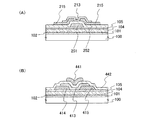
ここでは液晶表示装置を作製する例を、図1を用いて説明する。
ここでは有機薄膜トランジスタを用いたアクティブマトリクス型の発光装置を作製する例を、図2を用いて説明する。
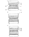
ここではパッシブマトリクス型の発光装置を作製する例を図4乃至図8を用いて説明する。
本実施の形態では、無線チップとして機能する半導体装置を作製する例を示す。本実施の形態で示す半導体装置は、非接触でデータの読み出しと書き込みが可能であることを特徴としており、データの伝送形式は、一対のコイルを対向に配置して相互誘導によって交信を行う電磁結合方式、誘導電磁界によって交信する電磁誘導方式、電波を利用して交信する電波方式の3つに大別されるが、いずれの方式を用いてもよい。
ここでは非晶質半導体層を用いた半導体素子を有する半導体装置を作製する例を、図14を用いて説明する。非晶質半導体層を用いた半導体素子としては、薄膜トランジスタ、ダイオード、抵抗素子等がある。ここでは、非晶質半導体層を用いた半導体素子としてダイオードを用いた光電変換素子の例を用いて示す。
本発明により得られる液晶表示装置や発光装置によって、様々なモジュール(アクティブマトリクス型液晶モジュール、アクティブマトリクス型ELモジュール)に用いることができる。即ち、それらを表示部に組み込んだ電子機器全てに本発明を実施できる。
本実施の形態では、実施の形態6に記載の表示部として用いることが可能な電気泳動表示装置を用いる例を示す。代表的には図15(C)に示す携帯書籍(電子書籍)の表示部3002、または表示部3003に適用する。
Claims (9)
- 基板上にシリコーン層を形成し、
前記シリコーン層の上面を全てプラズマ処理して脆弱層を形成し、
前記脆弱層上に有機化合物層を形成し、
前記有機化合物層上に非晶質半導体層を形成し、
前記非晶質半導体層を用いて半導体素子を形成した後、前記有機化合物層、及び前記半導体素子を含む積層体を前記基板から剥離する半導体装置の作製方法であって、
前記脆弱層は、前記シリコーン層の表面の有機基が酸化された層でなることを特徴とする半導体装置の作製方法。 - 基板上にシリコーン層を形成し、
前記シリコーン層の上面を全てプラズマ処理して脆弱層を形成し、
前記脆弱層上に有機化合物層を形成し、
前記有機化合物層上に有機化合物を有する半導体層を形成し、
前記有機化合物を有する半導体層を用いて半導体素子を形成した後、前記有機化合物層、及び前記半導体素子を含む積層体を前記基板から剥離する半導体装置の作製方法であって、
前記脆弱層は、前記シリコーン層の表面の有機基が酸化された層でなることを特徴とする半導体装置の作製方法。 - 基板上にシリコーン層を形成し、
前記シリコーン層の上面を全てプラズマ処理して脆弱層を形成し、
前記脆弱層上に有機化合物層を形成し、
前記有機化合物層上に第1の電極を形成し、
前記第1の電極上に発光層を形成し、
前記発光層上に第2の電極を形成し、
前記第2の電極上に可撓性基板を貼り付けた後、前記有機化合物層、前記第1の電極、前記発光層、及び前記第2の電極を含む積層体を前記基板から剥離する半導体装置の作製方法であって、
前記脆弱層は、前記シリコーン層の表面の有機基が酸化された層でなることを特徴とする半導体装置の作製方法。 - 基板上にシリコーン層を形成し、
前記シリコーン層の上面を全てプラズマ処理して脆弱層を形成し、
前記脆弱層上に有機化合物層を形成し、
前記有機化合物層上に印刷法により導電層を印刷した後焼成し、
前記導電層及び半導体部品を貼り付けた後、前記有機化合物層、及び前記導電層を含む積層体、並びに半導体部品を前記基板から剥離する半導体装置の作製方法であって、
前記脆弱層は、前記シリコーン層の表面の有機基が酸化された層でなることを特徴とする半導体装置の作製方法。 - 基板上にシリコーン層を形成し、
前記シリコーン層の上面を全てプラズマ処理して脆弱層を形成し、
前記脆弱層上に有機化合物層を形成し、
前記有機化合物層上に印刷法により導電層を印刷した後焼成し、前記有機化合物層、及び前記導電層を含む積層体を前記基板から剥離した後、前記導電層に半導体部品を接続する半導体装置の作製方法であって、
前記脆弱層は、前記シリコーン層の表面の有機基が酸化された層でなることを特徴とする半導体装置の作製方法。 - 請求項4または5において、
前記導電層は、アンテナであることを特徴とする半導体装置の作製方法。 - 請求項1乃至6のいずれか一において、
前記基板は、ガラス基板、セラミックス基板、或いは石英基板であることを特徴とする半導体装置の作製方法。 - 請求項1乃至7のいずれか一において、
前記脆弱層は、酸化珪素層であることを特徴とする半導体装置の作製方法。 - 請求項1乃至8のいずれか一において、
前記有機化合物層を塗布法により形成することを特徴とする半導体装置の作製方法。
Priority Applications (1)
| Application Number | Priority Date | Filing Date | Title |
|---|---|---|---|
| JP2008204280A JP5388500B2 (ja) | 2007-08-30 | 2008-08-07 | 半導体装置の作製方法 |
Applications Claiming Priority (3)
| Application Number | Priority Date | Filing Date | Title |
|---|---|---|---|
| JP2007224043 | 2007-08-30 | ||
| JP2007224043 | 2007-08-30 | ||
| JP2008204280A JP5388500B2 (ja) | 2007-08-30 | 2008-08-07 | 半導体装置の作製方法 |
Publications (3)
| Publication Number | Publication Date |
|---|---|
| JP2009076877A JP2009076877A (ja) | 2009-04-09 |
| JP2009076877A5 JP2009076877A5 (ja) | 2011-07-28 |
| JP5388500B2 true JP5388500B2 (ja) | 2014-01-15 |
Family
ID=40408198
Family Applications (1)
| Application Number | Title | Priority Date | Filing Date |
|---|---|---|---|
| JP2008204280A Expired - Fee Related JP5388500B2 (ja) | 2007-08-30 | 2008-08-07 | 半導体装置の作製方法 |
Country Status (3)
| Country | Link |
|---|---|
| US (1) | US7838328B2 (ja) |
| JP (1) | JP5388500B2 (ja) |
| KR (1) | KR101514627B1 (ja) |
Families Citing this family (55)
| Publication number | Priority date | Publication date | Assignee | Title |
|---|---|---|---|---|
| EP2002508A1 (en) * | 2006-03-17 | 2008-12-17 | Nxp B.V. | Antenna device and rf communication equipment |
| JP5371341B2 (ja) * | 2007-09-21 | 2013-12-18 | 株式会社半導体エネルギー研究所 | 電気泳動方式の表示装置 |
| JP5451036B2 (ja) * | 2008-11-21 | 2014-03-26 | 株式会社ジャパンディスプレイ | 表示装置及びその製造方法 |
| US9721825B2 (en) | 2008-12-02 | 2017-08-01 | Arizona Board Of Regents, A Body Corporate Of The State Of Arizona, Acting For And On Behalf Of Arizona State University | Method of providing a flexible semiconductor device and flexible semiconductor device thereof |
| WO2010065542A1 (en) | 2008-12-02 | 2010-06-10 | Arizona Board Of Regents, For And On Behalf Of Arizona State University | Method of preparing a flexible substrate assembly and flexible substrate assembly therefrom |
| US9991311B2 (en) | 2008-12-02 | 2018-06-05 | Arizona Board Of Regents On Behalf Of Arizona State University | Dual active layer semiconductor device and method of manufacturing the same |
| US9601530B2 (en) | 2008-12-02 | 2017-03-21 | Arizona Board Of Regents, A Body Corporated Of The State Of Arizona, Acting For And On Behalf Of Arizona State University | Dual active layer semiconductor device and method of manufacturing the same |
| CN101762922B (zh) | 2008-12-24 | 2012-05-30 | 京东方科技集团股份有限公司 | 触摸式电子纸及其制造方法 |
| EP2436029A4 (en) * | 2009-05-29 | 2013-04-10 | Univ Arizona | PROCESS FOR PROVIDING A FLEXIBLE SEMICONDUCTOR DEVICE AT HIGH TEMPERATURES AND FLEXIBLE SEMICONDUCTOR DEVICE THEREFOR |
| JP5632654B2 (ja) * | 2009-05-29 | 2014-11-26 | 株式会社半導体エネルギー研究所 | 表示装置 |
| KR101810699B1 (ko) * | 2009-06-30 | 2018-01-25 | 가부시키가이샤 한도오따이 에네루기 켄큐쇼 | 반도체 장치 제작 방법 |
| KR101470811B1 (ko) | 2009-09-16 | 2014-12-09 | 가부시키가이샤 한도오따이 에네루기 켄큐쇼 | 반도체 장치 |
| KR101519893B1 (ko) | 2009-09-16 | 2015-05-14 | 가부시키가이샤 한도오따이 에네루기 켄큐쇼 | 트랜지스터 |
| EP2486595B1 (en) * | 2009-10-09 | 2019-10-23 | Semiconductor Energy Laboratory Co. Ltd. | Semiconductor device |
| CN110061144A (zh) * | 2009-10-16 | 2019-07-26 | 株式会社半导体能源研究所 | 逻辑电路和半导体器件 |
| KR101763126B1 (ko) | 2009-11-06 | 2017-07-31 | 가부시키가이샤 한도오따이 에네루기 켄큐쇼 | 반도체 장치 및 그 제작 방법 |
| KR102450568B1 (ko) * | 2009-11-13 | 2022-10-07 | 가부시키가이샤 한도오따이 에네루기 켄큐쇼 | 반도체 장치 및 그 제작 방법 |
| WO2011068950A1 (en) * | 2009-12-03 | 2011-06-09 | The Trustees Of Columbia University In The City Of New York | Hierarchical assembly of nanostructured organic heterojunctions for photovoltaic devices |
| EP2362421A1 (en) | 2010-02-26 | 2011-08-31 | STMicroelectronics S.r.l. | Tailorable flexible sheet of monolithically fabricated array of separable cells each comprising a wholly organic, integrated circuit adapted to perform a specific function |
| JP2011181591A (ja) * | 2010-02-26 | 2011-09-15 | Sumitomo Chemical Co Ltd | 薄膜半導体装置、薄膜半導体製造装置及び薄膜半導体製造方法 |
| JP5565038B2 (ja) * | 2010-03-30 | 2014-08-06 | 凸版印刷株式会社 | 電界効果型トランジスタ及びその製造方法並びに画像表示装置 |
| WO2012021197A2 (en) | 2010-05-21 | 2012-02-16 | Arizona Board Of Regents, For And On Behalf Of Arizona State University | Method of manufacturing electronic devices on both sides of a carrier substrate and electronic devices thereof |
| WO2012021196A2 (en) | 2010-05-21 | 2012-02-16 | Arizona Board Of Regents, For And On Behalf Of Arizona State University | Method for manufacturing electronic devices and electronic devices thereof |
| JP2012015491A (ja) * | 2010-06-04 | 2012-01-19 | Semiconductor Energy Lab Co Ltd | 光電変換装置 |
| KR101856722B1 (ko) * | 2010-09-22 | 2018-05-10 | 가부시키가이샤 한도오따이 에네루기 켄큐쇼 | 파워 절연 게이트형 전계 효과 트랜지스터 |
| US20130308076A1 (en) * | 2010-10-01 | 2013-11-21 | Sharp Kabushiki Kaisha | Flexible display and method for manufacturing the same |
| US8912080B2 (en) | 2011-01-12 | 2014-12-16 | Semiconductor Energy Laboratory Co., Ltd. | Manufacturing method of the semiconductor device |
| JP5872912B2 (ja) * | 2011-01-21 | 2016-03-01 | 株式会社半導体エネルギー研究所 | 発光装置 |
| KR102040242B1 (ko) * | 2011-05-12 | 2019-11-05 | 가부시키가이샤 한도오따이 에네루기 켄큐쇼 | 발광 장치 및 발광 장치를 이용한 전자 기기 |
| TWI527207B (zh) | 2011-10-21 | 2016-03-21 | 友達光電股份有限公司 | 可撓式有機發光裝置及其製作方法 |
| JP5674707B2 (ja) * | 2012-05-22 | 2015-02-25 | 株式会社東芝 | 表示装置 |
| DE102012224424A1 (de) * | 2012-12-27 | 2014-07-17 | Robert Bosch Gmbh | Sensorsystem und Abdeckvorrichtung für ein Sensorsystem |
| US8878275B2 (en) * | 2013-02-18 | 2014-11-04 | Fairchild Semiconductor Corporation | LDMOS device with double-sloped field plate |
| KR20140122677A (ko) * | 2013-04-09 | 2014-10-20 | 주식회사 엘지화학 | 폴리이미드계 필름 및 이의 제조방법 |
| US10486359B2 (en) * | 2013-05-21 | 2019-11-26 | Sharp Kabushiki Kaisha | Method for manufacturing display apparatus, display apparatus, and film device |
| US10381224B2 (en) | 2014-01-23 | 2019-08-13 | Arizona Board Of Regents On Behalf Of Arizona State University | Method of providing an electronic device and electronic device thereof |
| WO2015156891A2 (en) | 2014-01-23 | 2015-10-15 | Arizona Board Of Regents, Acting For And On Behalf Of Arizona State University | Method of providing a flexible semiconductor device and flexible semiconductor device thereof |
| WO2017034644A2 (en) | 2015-06-09 | 2017-03-02 | ARIZONA BOARD OF REGENTS a body corporate for THE STATE OF ARIZONA for and on behalf of ARIZONA STATE UNIVERSITY | Method of providing an electronic device and electronic device thereof |
| JP2017518638A (ja) | 2014-05-13 | 2017-07-06 | アリゾナ・ボード・オブ・リージェンツ・フォー・アンド・オン・ビハーフ・オブ・アリゾナ・ステイト・ユニバーシティArizona Board Of Regents For And On Behalf Of Arizona State University | 電子デバイスを提供する方法およびその電子デバイス |
| US10008611B2 (en) | 2014-06-26 | 2018-06-26 | Joled Inc. | Thin film transistor and organic EL display device |
| DE202014103821U1 (de) * | 2014-07-09 | 2014-09-09 | Carmen Diegel | Flexible elektrische Leiterstruktur |
| US10446582B2 (en) | 2014-12-22 | 2019-10-15 | Arizona Board Of Regents On Behalf Of Arizona State University | Method of providing an imaging system and imaging system thereof |
| US9741742B2 (en) | 2014-12-22 | 2017-08-22 | Arizona Board Of Regents, A Body Corporate Of The State Of Arizona, Acting For And On Behalf Of Arizona State University | Deformable electronic device and methods of providing and using deformable electronic device |
| CN105118844A (zh) * | 2015-07-01 | 2015-12-02 | 深圳市华星光电技术有限公司 | 一种柔性显示面板的制备方法及柔性显示面板 |
| WO2017115225A2 (en) * | 2015-12-28 | 2017-07-06 | Semiconductor Energy Laboratory Co., Ltd. | Flexible device, display device, and manufacturing methods thereof |
| KR102499288B1 (ko) * | 2016-01-08 | 2023-02-14 | 삼성디스플레이 주식회사 | 표시 장치 |
| CN107808892B (zh) * | 2016-09-08 | 2020-06-26 | 群创光电股份有限公司 | 显示设备 |
| KR102079423B1 (ko) * | 2016-10-31 | 2020-02-19 | 주식회사 엘지화학 | 폴리이미드 필름 형성용 조성물 및 이를 이용하여 제조된 폴리이미드 필름 |
| CN106773206B (zh) * | 2016-12-26 | 2019-03-19 | 武汉华星光电技术有限公司 | 显示面板的制造方法 |
| CN106773207B (zh) * | 2016-12-26 | 2020-01-17 | 武汉华星光电技术有限公司 | 显示面板的制造方法 |
| CN206602182U (zh) * | 2017-04-06 | 2017-10-31 | 京东方科技集团股份有限公司 | 一种天线结构及通讯设备 |
| US20200372317A1 (en) * | 2018-02-13 | 2020-11-26 | Panasonic Intellectual Property Management Co., Ltd. | Wireless communication semiconductor device and manufacturing method therefor |
| JPWO2019203200A1 (ja) * | 2018-04-17 | 2021-05-13 | 凸版印刷株式会社 | 薄膜トランジスタアレイ、薄膜トランジスタアレイ多面付け基板、およびそれらの製造方法 |
| CN112310615B (zh) * | 2019-07-31 | 2023-03-28 | 庆鼎精密电子(淮安)有限公司 | 天线模组及其制备方法 |
| CN110838544A (zh) * | 2019-11-08 | 2020-02-25 | 福仕保(江苏)新材料有限公司 | 超薄柔性有机电子器件制备与封装一体式结构设计和制备流程工艺 |
Family Cites Families (14)
| Publication number | Priority date | Publication date | Assignee | Title |
|---|---|---|---|---|
| JP3364081B2 (ja) | 1995-02-16 | 2003-01-08 | 株式会社半導体エネルギー研究所 | 半導体装置の作製方法 |
| JP3406727B2 (ja) | 1995-03-10 | 2003-05-12 | 株式会社半導体エネルギー研究所 | 表示装置 |
| US5757456A (en) | 1995-03-10 | 1998-05-26 | Semiconductor Energy Laboratory Co., Ltd. | Display device and method of fabricating involving peeling circuits from one substrate and mounting on other |
| EP1039513A3 (en) | 1999-03-26 | 2008-11-26 | Canon Kabushiki Kaisha | Method of producing a SOI wafer |
| JP2001284622A (ja) * | 2000-03-31 | 2001-10-12 | Canon Inc | 半導体部材の製造方法及び太陽電池の製造方法 |
| US6489659B2 (en) * | 2000-04-20 | 2002-12-03 | Agere Systems Inc. | Non-hermetic APD |
| JP4027740B2 (ja) | 2001-07-16 | 2007-12-26 | 株式会社半導体エネルギー研究所 | 半導体装置の作製方法 |
| US8415208B2 (en) | 2001-07-16 | 2013-04-09 | Semiconductor Energy Laboratory Co., Ltd. | Semiconductor device and peeling off method and method of manufacturing semiconductor device |
| JP4836445B2 (ja) * | 2003-12-12 | 2011-12-14 | 株式会社半導体エネルギー研究所 | 半導体装置の作製方法 |
| US7439111B2 (en) | 2004-09-29 | 2008-10-21 | Semiconductor Energy Laboratory Co., Ltd. | Semiconductor device and manufacturing method thereof |
| JP2007251080A (ja) * | 2006-03-20 | 2007-09-27 | Fujifilm Corp | プラスチック基板の固定方法、回路基板およびその製造方法 |
| TWI427702B (zh) * | 2006-07-28 | 2014-02-21 | Semiconductor Energy Lab | 顯示裝置的製造方法 |
| JP4611270B2 (ja) * | 2006-09-27 | 2011-01-12 | Okiセミコンダクタ株式会社 | 半導体装置の製造方法 |
| US7968382B2 (en) * | 2007-02-02 | 2011-06-28 | Semiconductor Energy Laboratory Co., Ltd. | Method of manufacturing semiconductor device |
-
2008
- 2008-08-07 JP JP2008204280A patent/JP5388500B2/ja not_active Expired - Fee Related
- 2008-08-25 US US12/197,482 patent/US7838328B2/en not_active Expired - Fee Related
- 2008-08-26 KR KR1020080083209A patent/KR101514627B1/ko active IP Right Grant
Also Published As
| Publication number | Publication date |
|---|---|
| KR20090023158A (ko) | 2009-03-04 |
| US20090061721A1 (en) | 2009-03-05 |
| JP2009076877A (ja) | 2009-04-09 |
| KR101514627B1 (ko) | 2015-04-23 |
| US7838328B2 (en) | 2010-11-23 |
Similar Documents
| Publication | Publication Date | Title |
|---|---|---|
| JP5388500B2 (ja) | 半導体装置の作製方法 | |
| JP6175174B2 (ja) | 表示装置の作製方法 | |
| JP5305737B2 (ja) | 半導体装置 | |
| JP5651747B2 (ja) | 半導体装置 | |
| JP5364242B2 (ja) | 半導体装置の作製方法 | |
| TWI412138B (zh) | 半導體裝置,電子裝置,和半導體裝置的製造方法 | |
| JP2007027367A (ja) | 半導体装置の作製方法 |
Legal Events
| Date | Code | Title | Description |
|---|---|---|---|
| A521 | Request for written amendment filed |
Free format text: JAPANESE INTERMEDIATE CODE: A523 Effective date: 20110614 |
|
| A621 | Written request for application examination |
Free format text: JAPANESE INTERMEDIATE CODE: A621 Effective date: 20110614 |
|
| A977 | Report on retrieval |
Free format text: JAPANESE INTERMEDIATE CODE: A971007 Effective date: 20130627 |
|
| A131 | Notification of reasons for refusal |
Free format text: JAPANESE INTERMEDIATE CODE: A131 Effective date: 20130730 |
|
| A521 | Request for written amendment filed |
Free format text: JAPANESE INTERMEDIATE CODE: A523 Effective date: 20130909 |
|
| TRDD | Decision of grant or rejection written | ||
| A01 | Written decision to grant a patent or to grant a registration (utility model) |
Free format text: JAPANESE INTERMEDIATE CODE: A01 Effective date: 20131001 |
|
| A61 | First payment of annual fees (during grant procedure) |
Free format text: JAPANESE INTERMEDIATE CODE: A61 Effective date: 20131008 |
|
| R150 | Certificate of patent or registration of utility model |
Ref document number: 5388500 Country of ref document: JP Free format text: JAPANESE INTERMEDIATE CODE: R150 Free format text: JAPANESE INTERMEDIATE CODE: R150 |
|
| R250 | Receipt of annual fees |
Free format text: JAPANESE INTERMEDIATE CODE: R250 |
|
| R250 | Receipt of annual fees |
Free format text: JAPANESE INTERMEDIATE CODE: R250 |
|
| R250 | Receipt of annual fees |
Free format text: JAPANESE INTERMEDIATE CODE: R250 |
|
| LAPS | Cancellation because of no payment of annual fees |