WO2011102396A1 - Al alloy film for display device - Google Patents
Al alloy film for display device Download PDFInfo
- Publication number
- WO2011102396A1 WO2011102396A1 PCT/JP2011/053300 JP2011053300W WO2011102396A1 WO 2011102396 A1 WO2011102396 A1 WO 2011102396A1 JP 2011053300 W JP2011053300 W JP 2011053300W WO 2011102396 A1 WO2011102396 A1 WO 2011102396A1
- Authority
- WO
- WIPO (PCT)
- Prior art keywords
- alloy film
- display device
- precipitate
- film
- alloy
- Prior art date
Links
- 229910000838 Al alloy Inorganic materials 0.000 title claims abstract description 190
- 239000002244 precipitate Substances 0.000 claims abstract description 169
- 229910052761 rare earth metal Inorganic materials 0.000 claims abstract description 59
- 229910052719 titanium Inorganic materials 0.000 claims abstract description 17
- 229910052750 molybdenum Inorganic materials 0.000 claims abstract description 16
- 229910052721 tungsten Inorganic materials 0.000 claims abstract description 16
- 229910052715 tantalum Inorganic materials 0.000 claims abstract description 11
- 229910052735 hafnium Inorganic materials 0.000 claims abstract description 10
- 229910052758 niobium Inorganic materials 0.000 claims abstract description 10
- 229910052702 rhenium Inorganic materials 0.000 claims abstract description 10
- 229910052720 vanadium Inorganic materials 0.000 claims abstract description 10
- 229910052726 zirconium Inorganic materials 0.000 claims abstract description 10
- 238000010438 heat treatment Methods 0.000 claims description 70
- 239000004973 liquid crystal related substance Substances 0.000 claims description 22
- 239000012535 impurity Substances 0.000 claims description 18
- 229910052804 chromium Inorganic materials 0.000 claims description 15
- 229910052802 copper Inorganic materials 0.000 claims description 15
- 229910052759 nickel Inorganic materials 0.000 claims description 11
- 238000005477 sputtering target Methods 0.000 claims description 11
- 229910052697 platinum Inorganic materials 0.000 claims description 9
- 229910052782 aluminium Inorganic materials 0.000 claims description 8
- 230000007797 corrosion Effects 0.000 abstract description 22
- 238000005260 corrosion Methods 0.000 abstract description 22
- 230000015572 biosynthetic process Effects 0.000 abstract description 8
- 239000002245 particle Substances 0.000 abstract 1
- 238000001556 precipitation Methods 0.000 abstract 1
- 239000000047 product Substances 0.000 abstract 1
- 239000010408 film Substances 0.000 description 202
- 239000003513 alkali Substances 0.000 description 25
- 239000000463 material Substances 0.000 description 25
- 239000000243 solution Substances 0.000 description 24
- 239000010409 thin film Substances 0.000 description 23
- 239000000956 alloy Substances 0.000 description 21
- 238000000034 method Methods 0.000 description 21
- 229910045601 alloy Inorganic materials 0.000 description 20
- 239000000203 mixture Substances 0.000 description 17
- 229910052710 silicon Inorganic materials 0.000 description 17
- 238000004519 manufacturing process Methods 0.000 description 16
- 239000000758 substrate Substances 0.000 description 16
- 239000004065 semiconductor Substances 0.000 description 15
- 230000009471 action Effects 0.000 description 14
- 230000000694 effects Effects 0.000 description 14
- 230000008569 process Effects 0.000 description 13
- XUIMIQQOPSSXEZ-UHFFFAOYSA-N Silicon Chemical compound [Si] XUIMIQQOPSSXEZ-UHFFFAOYSA-N 0.000 description 11
- 239000010703 silicon Substances 0.000 description 11
- 229910021417 amorphous silicon Inorganic materials 0.000 description 9
- 229910000927 Ge alloy Inorganic materials 0.000 description 8
- 229910052751 metal Inorganic materials 0.000 description 7
- 239000002184 metal Substances 0.000 description 7
- 230000004888 barrier function Effects 0.000 description 6
- 229910052742 iron Inorganic materials 0.000 description 6
- 230000001681 protective effect Effects 0.000 description 6
- 239000003870 refractory metal Substances 0.000 description 6
- WGTYBPLFGIVFAS-UHFFFAOYSA-M tetramethylammonium hydroxide Chemical compound [OH-].C[N+](C)(C)C WGTYBPLFGIVFAS-UHFFFAOYSA-M 0.000 description 6
- 229910020637 Co-Cu Inorganic materials 0.000 description 5
- 150000001412 amines Chemical class 0.000 description 5
- 229910021419 crystalline silicon Inorganic materials 0.000 description 5
- 239000007789 gas Substances 0.000 description 5
- 229910021420 polycrystalline silicon Inorganic materials 0.000 description 5
- 238000012545 processing Methods 0.000 description 5
- XKRFYHLGVUSROY-UHFFFAOYSA-N Argon Chemical compound [Ar] XKRFYHLGVUSROY-UHFFFAOYSA-N 0.000 description 4
- 229910052581 Si3N4 Inorganic materials 0.000 description 4
- 238000004458 analytical method Methods 0.000 description 4
- 238000002149 energy-dispersive X-ray emission spectroscopy Methods 0.000 description 4
- 238000002474 experimental method Methods 0.000 description 4
- 230000003287 optical effect Effects 0.000 description 4
- HQVNEWCFYHHQES-UHFFFAOYSA-N silicon nitride Chemical compound N12[Si]34N5[Si]62N3[Si]51N64 HQVNEWCFYHHQES-UHFFFAOYSA-N 0.000 description 4
- 238000004544 sputter deposition Methods 0.000 description 4
- XLYOFNOQVPJJNP-UHFFFAOYSA-N water Substances O XLYOFNOQVPJJNP-UHFFFAOYSA-N 0.000 description 4
- 229910000881 Cu alloy Inorganic materials 0.000 description 3
- 239000007864 aqueous solution Substances 0.000 description 3
- 230000005540 biological transmission Effects 0.000 description 3
- 229910052796 boron Inorganic materials 0.000 description 3
- 238000005229 chemical vapour deposition Methods 0.000 description 3
- 238000004140 cleaning Methods 0.000 description 3
- 230000000052 comparative effect Effects 0.000 description 3
- 230000007547 defect Effects 0.000 description 3
- 238000010586 diagram Methods 0.000 description 3
- 239000011521 glass Substances 0.000 description 3
- 230000006872 improvement Effects 0.000 description 3
- AMGQUBHHOARCQH-UHFFFAOYSA-N indium;oxotin Chemical compound [In].[Sn]=O AMGQUBHHOARCQH-UHFFFAOYSA-N 0.000 description 3
- 239000011261 inert gas Substances 0.000 description 3
- 238000007689 inspection Methods 0.000 description 3
- 239000007788 liquid Substances 0.000 description 3
- 239000011159 matrix material Substances 0.000 description 3
- 238000005259 measurement Methods 0.000 description 3
- 238000000206 photolithography Methods 0.000 description 3
- 229920002120 photoresistant polymer Polymers 0.000 description 3
- 239000011347 resin Substances 0.000 description 3
- 229920005989 resin Polymers 0.000 description 3
- 230000004044 response Effects 0.000 description 3
- 239000000126 substance Substances 0.000 description 3
- IJGRMHOSHXDMSA-UHFFFAOYSA-N Atomic nitrogen Chemical compound N#N IJGRMHOSHXDMSA-UHFFFAOYSA-N 0.000 description 2
- 229910052779 Neodymium Inorganic materials 0.000 description 2
- 229910052786 argon Inorganic materials 0.000 description 2
- 239000000969 carrier Substances 0.000 description 2
- 230000003247 decreasing effect Effects 0.000 description 2
- 238000009616 inductively coupled plasma Methods 0.000 description 2
- 229910052746 lanthanum Inorganic materials 0.000 description 2
- 230000008018 melting Effects 0.000 description 2
- 238000002844 melting Methods 0.000 description 2
- 238000012986 modification Methods 0.000 description 2
- 230000004048 modification Effects 0.000 description 2
- XUIMIQQOPSSXEZ-NJFSPNSNSA-N silicon-30 atom Chemical compound [30Si] XUIMIQQOPSSXEZ-NJFSPNSNSA-N 0.000 description 2
- 238000007740 vapor deposition Methods 0.000 description 2
- 229910052688 Gadolinium Inorganic materials 0.000 description 1
- 239000000654 additive Substances 0.000 description 1
- 230000000996 additive effect Effects 0.000 description 1
- 239000012670 alkaline solution Substances 0.000 description 1
- 238000005275 alloying Methods 0.000 description 1
- 238000000137 annealing Methods 0.000 description 1
- 239000002585 base Substances 0.000 description 1
- 238000005266 casting Methods 0.000 description 1
- 230000008859 change Effects 0.000 description 1
- 239000000470 constituent Substances 0.000 description 1
- 238000002425 crystallisation Methods 0.000 description 1
- 230000008025 crystallization Effects 0.000 description 1
- 238000000280 densification Methods 0.000 description 1
- 238000009792 diffusion process Methods 0.000 description 1
- 238000009826 distribution Methods 0.000 description 1
- 235000012489 doughnuts Nutrition 0.000 description 1
- 230000005611 electricity Effects 0.000 description 1
- 238000010894 electron beam technology Methods 0.000 description 1
- 238000005516 engineering process Methods 0.000 description 1
- 238000005530 etching Methods 0.000 description 1
- 238000011156 evaluation Methods 0.000 description 1
- 238000004299 exfoliation Methods 0.000 description 1
- 230000008570 general process Effects 0.000 description 1
- 238000007654 immersion Methods 0.000 description 1
- 229910003437 indium oxide Inorganic materials 0.000 description 1
- PJXISJQVUVHSOJ-UHFFFAOYSA-N indium(iii) oxide Chemical compound [O-2].[O-2].[O-2].[In+3].[In+3] PJXISJQVUVHSOJ-UHFFFAOYSA-N 0.000 description 1
- 238000007733 ion plating Methods 0.000 description 1
- 229910052747 lanthanoid Inorganic materials 0.000 description 1
- 150000002602 lanthanoids Chemical class 0.000 description 1
- 238000001755 magnetron sputter deposition Methods 0.000 description 1
- 230000000873 masking effect Effects 0.000 description 1
- 239000000155 melt Substances 0.000 description 1
- 150000002736 metal compounds Chemical class 0.000 description 1
- 238000012544 monitoring process Methods 0.000 description 1
- 229910052757 nitrogen Inorganic materials 0.000 description 1
- 238000002559 palpation Methods 0.000 description 1
- 230000000737 periodic effect Effects 0.000 description 1
- 239000000843 powder Substances 0.000 description 1
- -1 pressure = 2 mTorr Substances 0.000 description 1
- 238000004445 quantitative analysis Methods 0.000 description 1
- 150000002910 rare earth metals Chemical class 0.000 description 1
- 229910000753 refractory alloy Inorganic materials 0.000 description 1
- 238000012827 research and development Methods 0.000 description 1
- 229910052706 scandium Inorganic materials 0.000 description 1
- SIXSYDAISGFNSX-UHFFFAOYSA-N scandium atom Chemical compound [Sc] SIXSYDAISGFNSX-UHFFFAOYSA-N 0.000 description 1
- 238000005245 sintering Methods 0.000 description 1
- 239000006104 solid solution Substances 0.000 description 1
- 238000009718 spray deposition Methods 0.000 description 1
- 230000008646 thermal stress Effects 0.000 description 1
- XOLBLPGZBRYERU-UHFFFAOYSA-N tin dioxide Chemical compound O=[Sn]=O XOLBLPGZBRYERU-UHFFFAOYSA-N 0.000 description 1
- 229910001887 tin oxide Inorganic materials 0.000 description 1
- 238000005406 washing Methods 0.000 description 1
- 229910052727 yttrium Inorganic materials 0.000 description 1
- VWQVUPCCIRVNHF-UHFFFAOYSA-N yttrium atom Chemical compound [Y] VWQVUPCCIRVNHF-UHFFFAOYSA-N 0.000 description 1
- YVTHLONGBIQYBO-UHFFFAOYSA-N zinc indium(3+) oxygen(2-) Chemical compound [O--].[Zn++].[In+3] YVTHLONGBIQYBO-UHFFFAOYSA-N 0.000 description 1
Images


Classifications
-
- C—CHEMISTRY; METALLURGY
- C23—COATING METALLIC MATERIAL; COATING MATERIAL WITH METALLIC MATERIAL; CHEMICAL SURFACE TREATMENT; DIFFUSION TREATMENT OF METALLIC MATERIAL; COATING BY VACUUM EVAPORATION, BY SPUTTERING, BY ION IMPLANTATION OR BY CHEMICAL VAPOUR DEPOSITION, IN GENERAL; INHIBITING CORROSION OF METALLIC MATERIAL OR INCRUSTATION IN GENERAL
- C23C—COATING METALLIC MATERIAL; COATING MATERIAL WITH METALLIC MATERIAL; SURFACE TREATMENT OF METALLIC MATERIAL BY DIFFUSION INTO THE SURFACE, BY CHEMICAL CONVERSION OR SUBSTITUTION; COATING BY VACUUM EVAPORATION, BY SPUTTERING, BY ION IMPLANTATION OR BY CHEMICAL VAPOUR DEPOSITION, IN GENERAL
- C23C14/00—Coating by vacuum evaporation, by sputtering or by ion implantation of the coating forming material
- C23C14/06—Coating by vacuum evaporation, by sputtering or by ion implantation of the coating forming material characterised by the coating material
- C23C14/14—Metallic material, boron or silicon
- C23C14/16—Metallic material, boron or silicon on metallic substrates or on substrates of boron or silicon
- C23C14/165—Metallic material, boron or silicon on metallic substrates or on substrates of boron or silicon by cathodic sputtering
-
- G—PHYSICS
- G09—EDUCATION; CRYPTOGRAPHY; DISPLAY; ADVERTISING; SEALS
- G09F—DISPLAYING; ADVERTISING; SIGNS; LABELS OR NAME-PLATES; SEALS
- G09F9/00—Indicating arrangements for variable information in which the information is built-up on a support by selection or combination of individual elements
- G09F9/30—Indicating arrangements for variable information in which the information is built-up on a support by selection or combination of individual elements in which the desired character or characters are formed by combining individual elements
-
- H—ELECTRICITY
- H01—ELECTRIC ELEMENTS
- H01L—SEMICONDUCTOR DEVICES NOT COVERED BY CLASS H10
- H01L21/00—Processes or apparatus adapted for the manufacture or treatment of semiconductor or solid state devices or of parts thereof
- H01L21/02—Manufacture or treatment of semiconductor devices or of parts thereof
- H01L21/04—Manufacture or treatment of semiconductor devices or of parts thereof the devices having at least one potential-jump barrier or surface barrier, e.g. PN junction, depletion layer or carrier concentration layer
- H01L21/18—Manufacture or treatment of semiconductor devices or of parts thereof the devices having at least one potential-jump barrier or surface barrier, e.g. PN junction, depletion layer or carrier concentration layer the devices having semiconductor bodies comprising elements of Group IV of the Periodic System or AIIIBV compounds with or without impurities, e.g. doping materials
- H01L21/28—Manufacture of electrodes on semiconductor bodies using processes or apparatus not provided for in groups H01L21/20 - H01L21/268
- H01L21/283—Deposition of conductive or insulating materials for electrodes conducting electric current
- H01L21/285—Deposition of conductive or insulating materials for electrodes conducting electric current from a gas or vapour, e.g. condensation
-
- H—ELECTRICITY
- H01—ELECTRIC ELEMENTS
- H01L—SEMICONDUCTOR DEVICES NOT COVERED BY CLASS H10
- H01L21/00—Processes or apparatus adapted for the manufacture or treatment of semiconductor or solid state devices or of parts thereof
- H01L21/02—Manufacture or treatment of semiconductor devices or of parts thereof
- H01L21/04—Manufacture or treatment of semiconductor devices or of parts thereof the devices having at least one potential-jump barrier or surface barrier, e.g. PN junction, depletion layer or carrier concentration layer
- H01L21/18—Manufacture or treatment of semiconductor devices or of parts thereof the devices having at least one potential-jump barrier or surface barrier, e.g. PN junction, depletion layer or carrier concentration layer the devices having semiconductor bodies comprising elements of Group IV of the Periodic System or AIIIBV compounds with or without impurities, e.g. doping materials
- H01L21/30—Treatment of semiconductor bodies using processes or apparatus not provided for in groups H01L21/20 - H01L21/26
- H01L21/31—Treatment of semiconductor bodies using processes or apparatus not provided for in groups H01L21/20 - H01L21/26 to form insulating layers thereon, e.g. for masking or by using photolithographic techniques; After treatment of these layers; Selection of materials for these layers
- H01L21/3205—Deposition of non-insulating-, e.g. conductive- or resistive-, layers on insulating layers; After-treatment of these layers
-
- H—ELECTRICITY
- H01—ELECTRIC ELEMENTS
- H01L—SEMICONDUCTOR DEVICES NOT COVERED BY CLASS H10
- H01L29/00—Semiconductor devices adapted for rectifying, amplifying, oscillating or switching, or capacitors or resistors with at least one potential-jump barrier or surface barrier, e.g. PN junction depletion layer or carrier concentration layer; Details of semiconductor bodies or of electrodes thereof ; Multistep manufacturing processes therefor
- H01L29/40—Electrodes ; Multistep manufacturing processes therefor
- H01L29/43—Electrodes ; Multistep manufacturing processes therefor characterised by the materials of which they are formed
- H01L29/45—Ohmic electrodes
- H01L29/456—Ohmic electrodes on silicon
- H01L29/458—Ohmic electrodes on silicon for thin film silicon, e.g. source or drain electrode
-
- H—ELECTRICITY
- H01—ELECTRIC ELEMENTS
- H01L—SEMICONDUCTOR DEVICES NOT COVERED BY CLASS H10
- H01L29/00—Semiconductor devices adapted for rectifying, amplifying, oscillating or switching, or capacitors or resistors with at least one potential-jump barrier or surface barrier, e.g. PN junction depletion layer or carrier concentration layer; Details of semiconductor bodies or of electrodes thereof ; Multistep manufacturing processes therefor
- H01L29/40—Electrodes ; Multistep manufacturing processes therefor
- H01L29/43—Electrodes ; Multistep manufacturing processes therefor characterised by the materials of which they are formed
- H01L29/49—Metal-insulator-semiconductor electrodes, e.g. gates of MOSFET
- H01L29/4908—Metal-insulator-semiconductor electrodes, e.g. gates of MOSFET for thin film semiconductor, e.g. gate of TFT
-
- H—ELECTRICITY
- H01—ELECTRIC ELEMENTS
- H01L—SEMICONDUCTOR DEVICES NOT COVERED BY CLASS H10
- H01L27/00—Devices consisting of a plurality of semiconductor or other solid-state components formed in or on a common substrate
- H01L27/02—Devices consisting of a plurality of semiconductor or other solid-state components formed in or on a common substrate including semiconductor components specially adapted for rectifying, oscillating, amplifying or switching and having at least one potential-jump barrier or surface barrier; including integrated passive circuit elements with at least one potential-jump barrier or surface barrier
- H01L27/12—Devices consisting of a plurality of semiconductor or other solid-state components formed in or on a common substrate including semiconductor components specially adapted for rectifying, oscillating, amplifying or switching and having at least one potential-jump barrier or surface barrier; including integrated passive circuit elements with at least one potential-jump barrier or surface barrier the substrate being other than a semiconductor body, e.g. an insulating body
- H01L27/1214—Devices consisting of a plurality of semiconductor or other solid-state components formed in or on a common substrate including semiconductor components specially adapted for rectifying, oscillating, amplifying or switching and having at least one potential-jump barrier or surface barrier; including integrated passive circuit elements with at least one potential-jump barrier or surface barrier the substrate being other than a semiconductor body, e.g. an insulating body comprising a plurality of TFTs formed on a non-semiconducting substrate, e.g. driving circuits for AMLCDs
- H01L27/124—Devices consisting of a plurality of semiconductor or other solid-state components formed in or on a common substrate including semiconductor components specially adapted for rectifying, oscillating, amplifying or switching and having at least one potential-jump barrier or surface barrier; including integrated passive circuit elements with at least one potential-jump barrier or surface barrier the substrate being other than a semiconductor body, e.g. an insulating body comprising a plurality of TFTs formed on a non-semiconducting substrate, e.g. driving circuits for AMLCDs with a particular composition, shape or layout of the wiring layers specially adapted to the circuit arrangement, e.g. scanning lines in LCD pixel circuits
-
- Y—GENERAL TAGGING OF NEW TECHNOLOGICAL DEVELOPMENTS; GENERAL TAGGING OF CROSS-SECTIONAL TECHNOLOGIES SPANNING OVER SEVERAL SECTIONS OF THE IPC; TECHNICAL SUBJECTS COVERED BY FORMER USPC CROSS-REFERENCE ART COLLECTIONS [XRACs] AND DIGESTS
- Y10—TECHNICAL SUBJECTS COVERED BY FORMER USPC
- Y10T—TECHNICAL SUBJECTS COVERED BY FORMER US CLASSIFICATION
- Y10T428/00—Stock material or miscellaneous articles
- Y10T428/31504—Composite [nonstructural laminate]
- Y10T428/31678—Of metal
Definitions
- the present invention is used for display devices such as liquid crystal displays and is useful as an electrode and wiring material for display device Al alloy films; display devices including the Al alloy films, and sputtering targets for forming the Al alloy films It is about.
- Al alloy films for display devices are mainly used as electrodes and wiring materials.
- electrodes and wiring materials gate electrodes, source and drain electrodes and wiring materials for thin film transistors in liquid crystal displays (LDC), organic EL (OELD) Gate, source and drain electrodes and wiring materials for thin film transistors, cathode and gate electrodes and wiring materials for field emission displays (FED), anode and wiring materials for fluorescent vacuum tubes (VFD), address electrodes for plasma displays (PDP) and Examples include wiring materials and back electrodes in inorganic EL.
- a liquid crystal display is typically taken up and described as a liquid crystal display device, but the present invention is not limited to this.
- liquid crystal display having a large size exceeding 100 inches has been commercialized, and a low power consumption technology has been developed, which is widely used as a main display device.
- Some liquid crystal displays have different operating principles. Among them, an active matrix type liquid crystal display using a thin film transistor (hereinafter referred to as TFT) for switching pixels has high-accuracy image quality. Because it can support high-speed video, it is the mainstay.
- TFTs using polycrystalline silicon or continuous grain boundary crystalline silicon as a semiconductor layer are used in liquid crystal displays that require further low power consumption and high-speed pixel switching.
- an active matrix liquid crystal display includes a TFT substrate having a TFT that is a switching element, a pixel electrode made of a conductive oxide film, and a wiring including a scanning line and a signal line. Are electrically connected to the pixel electrode.
- An Al-based alloy thin film is used as a wiring material constituting the scanning lines and signal lines.
- a scanning line 25 is formed on the glass substrate 1a, and a part of the scanning line 25 functions as a gate electrode 26 for controlling on / off of the TFT.
- the gate electrode 26 is electrically insulated by a gate insulating film (such as a silicon nitride film) 27.
- a semiconductor silicon layer 30 as a channel layer is formed through the gate insulating film 27, and a protective film (silicon nitride film or the like) 31 is further formed.
- the semiconductor silicon layer 30 is bonded to the source electrode 28 and the drain electrode 29 via the low resistance silicon layer 32 and has electrical conductivity.
- the drain electrode 29 has a structure in which the drain electrode 29 is in direct contact with the transparent electrode 5 such as ITO (Indium Tin Oxide) [referred to as a direct contact (DC). ]have.
- the transparent electrode 5 such as ITO (Indium Tin Oxide) [referred to as a direct contact (DC).
- Examples of the electrode wiring material used for direct contact include Al alloys described in Patent Documents 1 to 5. This is because Al has a small electrical resistivity and excellent fine workability. These Al alloys are directly connected to the oxide transparent conductive film constituting the transparent electrode or directly to the silicon semiconductor layer without interposing a barrier metal layer made of a refractory metal such as Mo, Cr, Ti, and W. Has been.
- These wiring films and electrodes 25 to 32 are covered with an insulating protective film 33 such as silicon nitride, and supply electricity to the drain electrode 29 through the transparent electrode 5.
- an insulating protective film 33 such as silicon nitride
- a manufacturing process of a liquid crystal display or the like includes a TFT heat treatment step. As a result, a part or the whole of the semiconductor silicon 30 having an amorphous structure is microcrystallized / polycrystallized. And the response speed of the TFT is improved.
- the insulating protective film 33 is deposited at a relatively low temperature of about 250 to 350 ° C.
- a high temperature heat treatment at about 450 ° C. or higher may be performed.
- such low temperature or high temperature heat treatment may be performed a plurality of times.
- Patent Documents 1 to 5 heat treatment is performed at about 200 to 350 ° C. for the purpose of reducing the contact resistance between the Al alloy wiring film and the transparent conductive film. No consideration was given to the heat resistance during high-temperature heating.
- the example of Patent Document 1 shows the results when the silicon nitride insulating film is formed at a temperature of 300 to 350 ° C. or the gate wiring film is formed at 250 ° C. No results are shown when heat treatment is performed at a higher temperature.
- Patent Document 2 was made for the purpose of providing an Al alloy material for TFT wiring that is particularly useful for low-temperature heat treatment, and it has been shown that low-temperature heat treatment at 200 ° C. is effective in Examples.
- Patent Document 3 shows the heat resistance evaluation results at 230 ° C. and 300 ° C., but does not evaluate the heat resistance when a higher temperature heat treatment is performed. The same applies to Patent Document 4.
- Patent Document 5 a part or all of a solid solution element in an Al alloy thin film is precipitated as a metal compound by heat treatment at 100 to 600 ° C. to obtain an Al alloy thin film having an electric resistance value of 10 ⁇ cm or less.
- the results in the examples are only shown when heated at a maximum temperature of 500 ° C., and the heat resistance when exposed to high temperatures of 500 ° C. or higher is not evaluated. Of course, no consideration is given to the heat resistance when exposed to such high temperatures multiple times.
- the hydrogenated amorphous silicon is microcrystallized and carrier mobility is improved.
- the heating temperature is higher and the heating time is longer, microcrystallization of hydrogenated amorphous silicon progresses and the mobility of carriers improves.
- the heat treatment temperature is increased, the Al alloy wiring thin film is caused by thermal stress.
- the upper limit of the heat treatment temperature when using an Al alloy thin film was set to about 350 ° C. at most. Therefore, when heat treatment is performed at a temperature higher than this, a refractory metal thin film such as Mo is generally used, but there is a problem that the wiring resistance is high and the display cannot be enlarged.
- contact resistance contact resistance
- the TFT substrate manufacturing process passes through a plurality of wet processes.
- a metal nobler than Al is added, a problem of galvanic corrosion appears and corrosion resistance deteriorates.
- an alkaline developer containing TMAH tetramethylammonium hydroxide
- the barrier metal layer is omitted, and the Al alloy film is exposed. It becomes easy to receive damage by. Therefore, it is required to be excellent in alkali corrosion resistance such as alkali developer resistance.
- the present invention has been made in view of the above circumstances.
- the object of the present invention is to generate no hillock even when exposed to a high temperature of about 450 to 600 ° C. and to be excellent in high-temperature heat resistance.
- Another object is to provide an Al alloy film for a display device that has a low wiring resistance and is excellent in alkali corrosion resistance such as alkali developer resistance.
- Another object of the present invention is preferably excellent in the stripping solution (stripping solution resistance) of the photosensitive resin, and when the barrier metal layer is omitted and directly connected to the transparent pixel electrode (transparent conductive film).
- An object of the present invention is to provide an Al alloy film for a display device which has a low contact resistance and can be directly connected (direct contact) with a transparent conductive film.
- the present invention includes the following aspects.
- An Al alloy film used in a display device includes at least one element selected from the group X consisting of Ta, Nb, Re, Zr, W, Mo, V, Hf, Ti, Cr and Pt, and at least one rare earth element,
- An Al alloy film for a display device which satisfies the following requirement (1) when the Al alloy film is subjected to a heat treatment at 450 to 600 ° C.
- (1) About the 1st precipitate containing Al, at least 1 type of element selected from said X group, and at least 1 type of the said rare earth elements, 500,000 pieces / mm of precipitates with a circle equivalent diameter of 20 nm or more Present at a density of 2 or more.
- the Al alloy film further contains at least one of Cu and Ge, and when the Al alloy film is subjected to a heat treatment at 450 to 600 ° C., it further satisfies the following requirement (2).
- the Al alloy film further contains at least one of Ni and Co.
- the following requirement (3) is further satisfied [2] ] Al alloy film for display apparatuses as described in above.
- the Al alloy film for a display device according to any one of [3] to [9], wherein the content of at least one of Ni and Co is 0.1 to 3 atomic%.
- the Al alloy film for a display device according to any one of [1] to [10], wherein the heat treatment is performed at 500 to 600 ° C.
- the Al alloy film for a display device according to any one of [1] to [11], wherein the heat treatment is performed at least twice.
- the Al alloy film for a display device according to any one of [2] to [12], wherein the Al alloy film is directly connected to a transparent conductive film.
- the Al alloy film is connected to the transparent conductive film via a film containing at least one element selected from the group consisting of Mo, Ti, W, and Cr.
- the sputtering target according to [15] further containing 0.1 to 2 atom% of at least one of Cu and Ge.
- a display device comprising the Al alloy film for a display device according to any one of [1] to [14].
- a liquid crystal display comprising the Al alloy film for a display device according to any one of [1] to [14].
- An organic EL display comprising the Al alloy film for a display device according to any one of [1] to [14].
- a field emission display comprising the Al alloy film for a display device according to any one of [1] to [14].
- a fluorescent vacuum tube comprising the Al alloy film for a display device according to any one of [1] to [14].
- a plasma display comprising the Al alloy film for a display device according to any one of [1] to [14].
- An inorganic EL display comprising the Al alloy film for a display device according to any one of [1] to [14].
- the first Al alloy film (Al—X group element—rare earth element alloy) according to the present invention is composed of a predetermined alloy element and the first precipitate, it is subjected to a high temperature of about 450 to 600 ° C. It was excellent in heat resistance when exposed to light, had good alkali corrosion resistance, and was able to keep the electrical resistance (wiring resistance) of the film itself after high temperature treatment low.
- the second Al alloy film (Al-X group element-rare earth element-Cu / Ge alloy) according to the present invention is composed of a predetermined alloy element, a first precipitate, and a second precipitate. Therefore, it shows higher heat resistance.
- the third Al alloy film (Al—X group element—rare earth element—Ni / Co—Cu / Ge alloy) according to the present invention includes a predetermined alloy element, a first precipitate, and a second precipitate.
- a predetermined alloy element e.g., aluminum, copper, copper, and zinc.
- the high-temperature heat treatment at about 450 to 600 ° C., and further, the high-temperature heat treatment is performed at least twice. Even when exposed to harsh high-temperature environments, the carrier mobility of the semiconductor silicon layer is increased, improving the TFT response speed and providing high-performance display devices that can handle energy savings and high-speed video. it can.
- FIG. 2 is an enlarged photograph (magnification 60,000 times) of a portion surrounded by a solid line in FIG.
- FIG. 3 is an enlarged photograph (magnification 150,000 times) of a portion surrounded by a solid line in FIG.
- FIG. 4 is an enlarged photograph (magnification 150,000 times) of a portion surrounded by a dotted line in FIG.
- FIG. 5 is a diagram showing a cross-sectional structure of the core portion of the thin film transistor.
- FIG. 6 is a diagram showing a Kelvin pattern (TEG pattern) used for measuring the contact resistance between the Al alloy film and the transparent pixel electrode.
- FIGS. 7A to 7F are EDX plane analysis photographs of the precipitates shown in FIGS. 3 and 4 (FIG. 3: Precipitate 1, Precipitate 2; FIG. 4: Precipitate 3).
- FIG. 8 is a schematic cross-sectional view showing an example of a liquid crystal display.
- FIG. 9 is a schematic cross-sectional view showing an example of an organic EL display.
- FIG. 10 is a schematic cross-sectional view showing an example of a field emission display.
- FIG. 11 is a schematic cross-sectional view showing an example of a fluorescent vacuum tube.
- FIG. 12 is a schematic cross-sectional view showing an example of a plasma display.
- FIG. 13 is a schematic cross-sectional view showing an example of an inorganic EL display.
- the inventors of the present invention are excellent in high-temperature heat resistance without generating hillocks even when exposed to a high temperature of about 450 to 600 ° C., and the electric resistance (wiring resistance) of the film itself is kept low.
- Al alloy film for display device having high alkali corrosion resistance such as alkali developer (sometimes referred to as first Al alloy film); more preferably for display device having higher high temperature heat resistance Al alloy film (sometimes referred to as a second Al alloy film); Furthermore, it preferably has excellent resistance to stripping solution at high temperatures, and has low contact resistance even when directly connected to a transparent conductive film.
- studies have been repeated.
- At least one element selected from the group consisting of Ta, Nb, Re, Zr, W, Mo, V, Hf, Ti, Cr, and Pt (group X) and at least one rare earth element (REM)
- group X at least one element selected from the group consisting of Ta, Nb, Re, Zr, W, Mo, V, Hf, Ti, Cr, and Pt
- group X at least one element selected from the group consisting of Ta, Nb, Re, Zr, W, Mo, V, Hf, Ti, Cr, and Pt
- group REM rare earth element
- the requirement (1) above it was found that the second Al alloy film that satisfies the following requirements and satisfies the requirement (2) below exhibits higher heat resistance.
- the second precipitate containing Al, Cu and / or Ge, and at least one rare earth element precipitates having an equivalent circle diameter of 200 nm or more exist at a density of 10,000 pieces / mm 2 or more. .
- Al alloy film Al—X group element—REM—Ni / Co—Cu / Ge alloy film
- the third Al alloy film satisfying the requirements of 1) and (2) and satisfying the requirement of (3) below can not only solve the above-mentioned problems caused by the first Al alloy film, but also can be a preferable problem (high temperature It has been found that high stripping solution resistance during processing and contact resistance with the transparent conductive film can be solved at the same time.
- the first Al alloy film contains an X-group element (high temperature heat resistance improving element) of a refractory metal and a rare earth element (alkali corrosion resistance improving element) in the Al alloy, and a predetermined first precipitate. Because it has high heat resistance (high temperature heat resistance) and alkali corrosion resistance at high temperatures and excellent electrical resistance (wiring resistance) of the film itself, wiring such as scanning lines and signal lines It is suitably used as a material for electrodes such as a gate electrode, a source electrode, and a drain electrode. In particular, it is suitably used as a gate electrode of a thin film transistor substrate and a related wiring film material that are easily affected by high temperature thermal history.
- the second Al alloy film contains Cu and / or Ge (an element for improving the peeling solution resistance) in addition to the X group element and the rare earth element in the Al alloy. Therefore, the heat resistance under high temperature (high temperature heat resistance) is further enhanced, and it is suitably used as a material for electrodes such as wiring for scanning lines and signal lines; gate electrodes, source electrodes, drain electrodes, etc. . In particular, it is suitably used as a gate electrode of a thin film transistor substrate and a related wiring film material that are easily affected by high temperature thermal history.
- the third Al alloy film includes, in the Al alloy, Ni and / or Co (element for reducing contact resistance with a transparent conductive film), Cu and / or Ge in addition to the X group element and the rare earth element. Electrode / wiring for direct contact that can be directly connected to the transparent conductive film without intervening a barrier metal layer because it contains the (exfoliation liquid resistance improving element) and has a predetermined third precipitate. It is suitably used as the material.
- high temperature heat resistance means that hillocks do not occur when exposed to a high temperature of at least about 450 to 600 ° C., and preferably, it is repeatedly exposed at least twice or more to the high temperature described above. This means that no hillock will occur.
- the first Al alloy film includes at least one element selected from the group consisting of Ta, Nb, Re, Zr, W, Mo, V, Hf, Ti, Cr and Pt (group X), and a rare earth element ( REM) is an Al—X group element-REM alloy film.
- the group X element (group X element) is composed of a refractory metal having a melting point of approximately 1600 ° C. or higher, and is an element that contributes to improving heat resistance at high temperatures. These elements may be added alone or in combination of two or more. Of the group X elements, Ta and Ti are preferable, and Ta is more preferable.
- the content of the X group element (when contained alone, it is a single amount, and when two or more types are used in combination) is preferably from 0.1 to 5 atomic%. If the content of the X group element is less than 0.1 atomic%, the above effect may not be exhibited effectively. On the other hand, if the content of the X group element exceeds 5 atomic%, the electrical resistance of the Al alloy film may be excessively high, and there may be a problem that a residue is easily generated during wiring processing.
- a more preferable content of the group X element is 0.1 atomic% or more and 3.0 atomic% or less, and a more preferable content is 0.3 atomic% or more and 2.0 atomic% or less.
- the rare earth element is an element that contributes to improvement of high temperature heat resistance by being added in combination with the X group element. Furthermore, it has an effect that the X group element does not have, such as corrosion resistance in an alkaline environment alone.
- the rare earth element is an element group in which Sc (scandium) and Y (yttrium) are added to a lanthanoid element (a total of 15 elements from La with atomic number 57 to Lu with atomic number 71 in the periodic table).
- the rare earth elements may be used alone or in combination of two or more.
- the rare earth elements Nd, La, and Gd are preferable, and Nd and La are more preferable.
- the rare earth element content (individual amount when contained alone, and total amount when two or more kinds are used in combination) is 0.1. It is preferably ⁇ 4 atomic%. If the rare earth element content is less than 0.1 atomic%, the alkali corrosion resistance may not be exhibited effectively. On the other hand, if it exceeds 4 atomic%, the electrical resistance of the Al alloy film itself may be too high. There is a possibility that a residue may be easily generated during wiring processing.
- the more preferable content of the rare earth element is 0.3 atomic% or more and 3.0 atomic% or less, and the more preferable content is 0.5 atomic% or more and 2.5 atomic% or less.
- Examples of the first Al alloy film include an Al alloy film that contains the above-described elements and is the balance: Al and inevitable impurities.
- examples of the inevitable impurities include Fe, Si, and B. Although the total amount of inevitable impurities is not particularly limited, it may be contained in an amount of about 0.5 atomic% or less.
- Each inevitable impurity element has B of 0.012 atomic% or less, and Fe and Si each have a content of 0. You may contain 12 atomic% or less.
- the first Al alloy film is subjected to high-temperature heat treatment at 450 to 600 ° C. to form a first precipitate (Al-X group element-REM-containing precipitate) having a predetermined size and a density specified in (1) above.
- a first precipitate Al-X group element-REM-containing precipitate
- the first precipitate only needs to contain at least the X group element and REM, and may contain other elements as long as the action of the precipitate is not hindered.
- the circle equivalent diameter (size) of the first precipitate is 20 nm or more. According to the examination results of the present inventors, it has been found that a precipitate having a thickness of less than 20 nm does not exhibit a desired effect even if the composition of the precipitate is an Al—X group element-REM-containing precipitate.
- the lower limit of the equivalent circle diameter may be 20 nm, and the upper limit is not particularly limited in relation to the above action, but the size of the precipitate is large. When it becomes a huge precipitate, it may be visually recognized by an inspection with an optical microscope, and there is a possibility that an appearance defect may be caused. Therefore, the upper limit is preferably 1 ⁇ m.
- a preferable equivalent circle diameter of the first precipitate is 20 nm or more and 800 nm or less.
- the precipitates having an equivalent circle diameter of 20 nm or more exist at a density of 500,000 pieces / mm 2 or more. According to the examination results of the present inventors, it has been found that the desired effect is not exhibited when the size of the first precipitate is 20 nm or more and is less than 500,000 pieces / mm 2 .
- the density of the precipitate is preferably as high as possible, and is preferably 2,000,000 pieces / mm 2 or more.
- the second Al alloy film is an Al—X group element-REM—Cu / Ge alloy film containing Cu and / or Ge in addition to the X group element and rare earth element (REM) described above.
- Cu and / or Ge contribute to the improvement of the high temperature heat resistance and have the action of preventing the generation of hillocks under the high temperature process.
- the second Al alloy film only needs to contain at least the X group element and REM and Cu and / or Ge, and may contain other elements as long as the action of these additive elements is not hindered. good.
- Cu and / or Ge may be added alone or both may be added.
- the content of Cu and / or Ge (single content in the case of a single substance, and the total amount in the case of containing both) is 0.1 to 2 It is preferable to use atomic%.
- the content of Cu and / or Ge is less than 0.1 atomic%, the desired effect may not be obtained, and the density of the second precipitate contributing to further improvement in heat resistance may not be ensured.
- the electrical resistivity may increase.
- a more preferable content of the element is 0.1 atomic% or more and 1.0 atomic% or less, and more preferably 0.1 atomic% or more and 0.6 atomic% or less.
- the second Al alloy film is subjected to high-temperature heat treatment at 450 to 600 ° C. to form second precipitates (Al-REM-Cu / Ge-containing precipitates) having a predetermined size and a density specified in (2) above. Accordingly, it is possible to realize high peeling solution resistance at high temperatures and low contact resistance with the transparent conductive film.
- the second precipitate only needs to contain at least a rare earth element and Cu and / or Ge, and may contain other elements as long as the action of the precipitate is not hindered.
- the circle equivalent diameter (size) of the second precipitate is 200 nm or more. According to the examination results of the present inventors, it has been found that a precipitate having a thickness of less than 200 nm does not exhibit a desired effect even if the composition of the precipitate satisfies the above composition.
- the lower limit of the equivalent circle diameter may be 200 nm, and the upper limit is not particularly limited in relation to the above action, but the size of the precipitate increases and becomes huge. When it becomes a precipitate, it may be visually recognized by inspection with an optical microscope, and it causes an appearance defect. Therefore, the upper limit is preferably 1 ⁇ m.
- a preferable equivalent circle diameter of the second precipitate is 200 nm or more and 800 nm or less.
- the density of the precipitate is preferably as high as possible, and preferably 25,000 / mm 2 or more.
- Examples of the second Al alloy film include an Al alloy film containing the above-described elements, and the balance: Al and inevitable impurities.
- examples of the inevitable impurities include Fe, Si, and B. Although the total amount of inevitable impurities is not particularly limited, it may be contained in an amount of about 0.5 atomic% or less. Each inevitable impurity element has B of 0.012 atomic% or less, and Fe and Si each have a content of 0. You may contain 12 atomic% or less.
- the third Al alloy film includes an Al—X group element-REM— containing Ni and / or Co in addition to the above-described X group element and rare earth element (REM) and the above-described Cu and / or Ge. It is a Ni / Co—Cu / Ge alloy film.
- Ni and Co are elements that enable direct connection (direct contact) with the transparent conductive film. This is because electrical conduction with the transparent conductive film becomes possible through highly conductive Ni and / or Co-containing Al-based precipitates formed by the thermal history in the TFT manufacturing process. These may be added alone or both may be added.
- the content of Ni and / or Co (single content in the case of a single substance and the total amount in the case of containing both) is 0.1 to 3 It is preferable to use atomic%.
- the content of Ni and / or Co is less than 0.1 atomic%, the desired effect cannot be obtained, and the density of the third precipitate that contributes to reducing the contact resistance with the transparent conductive film may not be ensured. . That is, since the size of the third precipitate is small and the density is also reduced, it is difficult to stably maintain a low contact resistance with the transparent conductive film.
- the content of Ni and / or Co exceeds 3 atomic%, the corrosion resistance in an alkaline environment may be lowered.
- the more preferable content of Ni and / or Co is 0.1 atomic% or more and 1.0 atomic% or less, and further preferably 0.1 atomic% or more and 0.6 atomic% or less.
- Cu and / or Ge is an element that enables direct connection (direct contact) with the transparent conductive film when used in combination with the above-described Ni and / or Co.
- the desired third Precipitates can be secured.
- the third Al alloy film is subjected to high-temperature heat treatment at 450 to 600 ° C. to form third precipitates (Al—REM—Ni / Co—Cu / Ge) having a predetermined size and a density specified in (3) above. Containing precipitates), and thereby, high stripping solution resistance at high temperatures and low contact resistance with the transparent conductive film can be realized.
- the third precipitate may contain at least a rare earth element, Ni and / or Co, Cu and / or Ge, and may contain other elements as long as the action of the precipitate is not hindered. Also good.
- the circle equivalent diameter (size) of the third precipitate is 200 nm or more. According to the examination results of the present inventors, it has been found that a precipitate having a thickness of less than 200 nm does not exhibit a desired effect even if the composition of the precipitate satisfies the above composition.
- the lower limit of the equivalent circle diameter may be 200 nm, and the upper limit is not particularly limited in relation to the above action, but the size of the precipitate increases and becomes huge. When it becomes a precipitate, it may be visually recognized by an inspection with an optical microscope, and there is a possibility of causing an appearance defect. Therefore, the upper limit is preferably 3 ⁇ m.
- a preferable equivalent circle diameter of the third precipitate is 200 nm or more and 2 ⁇ m or less.
- the density of the precipitates is preferably as high as possible and preferably 5000 / mm 2 or more.
- Examples of the third Al alloy film include an Al alloy film containing the above elements and having the balance: Al and inevitable impurities.
- the inevitable impurities include Fe, Si, and B. Although the total amount of inevitable impurities is not particularly limited, it may be contained in an amount of about 0.5 atomic% or less.
- Each inevitable impurity element has B of 0.012 atomic% or less, and Fe and Si each have a content of 0. You may contain 12 atomic% or less.
- the heat treatment for forming the first to third precipitates is 450 to 600 ° C., preferably 500 to 600 ° C.
- This heat treatment is preferably performed in a vacuum or nitrogen and / or inert gas atmosphere, and the treatment time is preferably 1 minute or more and 60 minutes or less. According to the present invention, it has been found that hillocks and the like do not occur even when the above heat treatment (high temperature heat treatment) is performed twice or more.
- the TFT manufacturing process corresponding to such high temperature heat treatment includes, for example, annealing by laser for crystallizing amorphous silicon, film formation by CVD (chemical vapor deposition) for various thin film formation, impurity diffusion And the temperature of a heat treatment furnace when the protective film is thermally cured.
- the heat treatment for crystallization of amorphous silicon is often exposed to the high temperatures as described above.
- the film thickness of the Al alloy is preferably 50 nm or more, and more preferably 100 nm or more, particularly in order to ensure high temperature heat resistance and reduced wiring resistance.
- the upper limit is not particularly limited from the above viewpoint, but it is preferably 1 ⁇ m or less, more preferably 600 nm or less in consideration of the wiring taper shape and the like.
- the upper limit and the lower limit of the film thickness can be arbitrarily combined to make the film thickness range.
- the Al alloy film is preferably used for various wiring materials such as a source-drain electrode and a gate electrode.
- the Al alloy film is more preferably used as a wiring material for a gate electrode requiring high temperature heat resistance.
- the Al alloy film is preferably formed by a sputtering method using a sputtering target (hereinafter also referred to as “target”). This is because a thin film having excellent in-plane uniformity of components and film thickness can be easily formed as compared with a thin film formed by ion plating, electron beam vapor deposition or vacuum vapor deposition.
- the Al alloy sputtering target having the same composition as that of the desired Al alloy film is used as the target, There is no fear, and an Al alloy film having a desired component composition can be formed.
- the present invention also includes a sputtering target having the same composition as that of the first, second, or third Al alloy film described above. Specifically, as the above target, (i) at least one element selected from the group consisting of Ta, Nb, Re, Zr, W, Mo, V, Hf, Ti, Cr, and Pt (group X) is set to 0.8.
- At least one kind of rare earth element is contained in an amount of 0.1 to 4 atom%, and the balance: Al and an inevitable impurity target, (ii) Ta, Nb, Re, Zr, W, Mo 0.1 to 5 atomic% of at least one element selected from the group consisting of V, Hf, Ti, Cr and Pt (group X), and 0.1 to 4 atomic% of at least one rare earth element
- group X 0.1 to 2 atomic% of Cu and / or Ge
- the shape of the target includes a shape processed into an arbitrary shape (a square plate shape, a circular plate shape, a donut plate shape, etc.) according to the shape and structure of the sputtering apparatus.
- a method for producing the above target a method of producing an ingot made of an Al-based alloy by a melt casting method, a powder sintering method, or a spray forming method, or a preform made of an Al-based alloy (the final dense body is prepared)
- Examples thereof include a method obtained by producing an intermediate before being obtained) and then densifying the preform by a densification means.
- the present invention includes a display device characterized in that the Al alloy film is used in a thin film transistor.
- the Al alloy film is used for a source electrode and / or a drain electrode and a signal line of a thin film transistor, and the drain electrode is directly connected to a transparent conductive film, or used for a gate electrode and a scanning line. And the like.
- a refractory metal film or a refractory alloy film (barrier metal) containing at least one element selected from the group consisting of Mo, Ti, W, and Cr is used. It is preferable to be connected to a transparent conductive film.
- the third Al alloy film is used, it is preferable that the third Al alloy film is directly connected to the transparent conductive film without using the barrier metal.
- the gate electrode and the scanning line, the source electrode and / or the drain electrode, and the signal line are included in the form of an Al alloy film having the same composition.
- the transparent pixel electrode used in the present invention is not particularly limited, and examples thereof include indium tin oxide (ITO) and indium zinc oxide (IZO).
- the semiconductor layer used in the present invention is not particularly limited, and examples thereof include amorphous silicon, polycrystalline silicon, and continuous grain boundary crystalline silicon.
- the liquid crystal display is typically taken up and described as the liquid crystal display device, but the above-described Al alloy film for display device of the present invention described above can be used for various liquid crystal display devices mainly as electrodes and wiring materials.
- the cathode and gate electrodes and the wiring material in the field emission display (FED) illustrated in FIG. 10 for example, the anode electrode and the wiring material in the fluorescent vacuum tube (VFD) illustrated in FIG. 11, for example, the plasma display illustrated in FIG. 12.
- Al alloy targets having various compositions prepared by a vacuum melting method were used as sputtering targets.
- the content of each alloy element in various Al alloy films used in the examples was determined by an ICP emission analysis (inductively coupled plasma emission analysis) method.
- the Al alloy film formed as described above is subjected to high-temperature heat treatment at 450 to 600 ° C. twice, and the Al alloy film after the high-temperature heat treatment is subjected to heat resistance and electrical resistance (arrangement of the Al alloy film itself). Resistance), contact resistance when the Al alloy film is directly connected to the transparent pixel electrode (contact resistance with ITO), stripping liquid resistance, and the size and density of the precipitates, respectively, as shown below Measured with For reference, an experiment at 350 ° C. was also conducted for heat resistance. In addition, about alkali developing solution tolerance, it experimented using the Al alloy film after film-forming, and heat processing was not performed.
- the reason for exposure to an alkaline environment in the TFT manufacturing process is a photolithography process for forming an Al alloy wiring, which is a stage before receiving a thermal history.
- Alkali developer resistance (developer etch rate measurement) After masking the Al alloy film formed on the substrate, it was immersed in a developer (aqueous solution containing 2.38% by mass of TMAH) at 25 ° C. for 5 minutes, and the etching amount was measured using a palpation type step gauge. did. Alkali developer resistance was evaluated according to the criteria shown in Table 8, and in this example, ⁇ or ⁇ was accepted.
- the number of crater-like corrosion (pitting corrosion) marks (those with an equivalent circle diameter of 150 nm or more) found on the film surface after immersion was examined (observation magnification was 1000 times).
- the stripping solution resistance was evaluated according to the judgment criteria shown in Table 8, and in this example, “ ⁇ ” or “ ⁇ ” was accepted.
- the precipitate size (550 ° C./600° C.) “ ⁇ ” means that the first to third precipitates also have the size “ ⁇ ” (also “ ⁇ ” and “ ⁇ ”). The same).
- the density of precipitates (550 ° C./600° C.) is “ ⁇ ”, meaning that the density of both the first precipitate and the second precipitate is“ ⁇ ”(the same applies to“ ⁇ ”and“ ⁇ ”). ).
- the precipitate size (550 ° C./600° C.) and the precipitate density (550 ° C./600° C.) are “ ⁇ ”.
- the size and density of both the first to third precipitates are “ ⁇ ”. Means.
- the precipitate size (550 ° C./600° C.) and the precipitate density (550 ° C./600° C.) are “ ⁇ ”
- the size and density of both the first to third precipitates are both “ ⁇ ”.
- Each of the Al alloy films shown in Tables 1 to 5 corresponds to the third Al alloy film according to the present invention, satisfies the alloy composition defined in the present invention, and has the first to third precipitates. Therefore, not only is the heat resistance at low temperature (350 ° C.) excellent, but also the heat resistance at 450 to 600 ° C. is excellent. Furthermore, the electrical resistance after high-temperature heat treatment has a lower electrical resistance than refractory metals, has good resistance to alkaline developer and stripper after high-temperature heat treatment, and ITO (transparent pixel electrode) and The direct contact resistance can be greatly reduced.
- No. 43 shows the results when heat-treating an Al-0.5 atomic% Ta-2.0 atomic% La-0.1 atomic% Ni-0.5 atomic% Ge alloy film at 550 ° C. And the following precipitates were obtained when treated at any temperature of 600 ° C.
- the third precipitate (Al—Ni—Ge—La-containing precipitate) has a size (equivalent circle diameter): ⁇ (200 nm to 800 nm), and a density (pieces / mm 2 ): ⁇ (5,000 / Mm 2 or more).
- Table 9 shows the results of analyzing the composition of each precipitate by the EDX semi-quantitative method for the precipitates (1 to 4) present in 43.
- the precipitates (1 to 4) refer to the precipitates observed in FIGS.
- FIG. 3 shows precipitates 1 and 2
- FIG. 4 shows precipitates 3 and 4, respectively. Since these precipitates have various sizes and are widely dispersed in the Al alloy film, a photograph showing a change in magnification is shown, and FIG. 2 (magnification 60,000 times) is a diagram. 1 (magnification of 30,000 times) and FIGS.
- FIG. 7 (a) to 7 (f) are EDX plane analysis photographs of the precipitates shown in FIGS. 3 and 4 (FIG. 3: Precipitate 1, Precipitate 2; FIG. 4: Precipitate 3). .
- the precipitate size (550 ° C./600° C.) and the precipitate density (550 ° C./600° C.) are “xxx” (see Nos. 1 to 9 in Table 6).
- the first precipitate, the second precipitate, and the third precipitate also mean “x” in both size and density.
- the precipitate size (550 ° C./600° C.) and the precipitate density (550 ° C./600° C.) are “ ⁇ ⁇ ” (see Nos. 10 to 13 in Table 6).
- the size and density of the first precipitate are both “x”, but the size and density of the second precipitate and the third precipitate are both “ ⁇ ”.
- the precipitate size (550 ° C./600° C.) and the precipitate density (550 ° C./600° C.) are “ ⁇ XX” (Nos. 16 to 21, 56, 57, 59 in Table 6).
- ⁇ 62, 64 to 69) means that the size and density of the first precipitate are both “ ⁇ ”, but the size and density of the second precipitate and the third precipitate are both “ ⁇ ”.
- the precipitate size (550 ° C./600° C.) is “ ⁇ xx”
- the precipitate density (550 ° C./600° C.) is “ ⁇ XX” (No. in Tables 6 and 7).
- the first precipitate size is “ ⁇ ”
- the first precipitate density is “ ⁇ ”
- the second precipitate size means that the first precipitate size is “ ⁇ ”
- the second precipitate size means that the second precipitate size.
- density means “x”.
- the precipitate size (550 ° C./600° C.) and the precipitate density (550 ° C./600° C.) are “ ⁇ ⁇ ” (Nos. 24 to 27, 30 to 45 in Tables 6 and 7).
- 48-51, 54, and 55) the size and density of the first precipitate and the second precipitate are both “ ⁇ ”, but the size and density of the third precipitate are both "X" means.
- the precipitate size (550 ° C./600° C.) is “ ⁇ ⁇ ”
- the precipitate density (550 ° C./600° C.) is “ ⁇ XX” (No. in Tables 6 and 7).
- 22, 23, 28, 29, 46, 47, 52, 53) is the first precipitate
- the second precipitate size is “ ⁇ ”
- the second precipitate The density is “ ⁇ ”
- the third precipitate size and density both mean “x”.
- Each of the Al alloy films 14 to 21 and 56 to 69 corresponds to the first Al alloy film according to the present invention, and the alloy composition defined in the present invention (strictly, Nos. 14 to 21 are the X group).
- Ni / Co is also contained
- the requirements (size and density) of the first precipitate are also satisfied, so that the low temperature range (350 ° C.) to the high temperature range Excellent heat resistance over a wide range (450-600 ° C). Furthermore, it is excellent in low electrical resistance after high-temperature heat treatment, high stripping solution resistance, and alkali developer resistance.
- these Al alloy films do not contain Cu and / or Ge, the requirements (size and density) of the second precipitate and the third precipitate are not satisfied. Decreased, and the contact resistance with ITO increased.
- Each of the Al alloy films 22 to 55 also corresponds to the second Al alloy film according to the present invention, and the alloy composition defined in the present invention (strictly speaking, in addition to the X group element and the rare earth, further Ge or Cu
- the requirements (size and density) of the first precipitate are also satisfied, so that it is widely used from a low temperature range (350 ° C.) to a high temperature range (450 to 600 ° C.). Excellent heat resistance. Furthermore, it is excellent in low electrical resistance after high-temperature heat treatment, high stripping solution resistance, and alkali developer resistance.
- these Al alloy films do not contain Ni and / or Co, the requirements (size and density) of the third precipitate are not satisfied. The contact resistance of became high.
- No. in Table 6 2/3 is a comparative example that contains only Ni / Co and does not contain the X group element and rare earth element, and since none of the desired first, second, and third precipitates can be obtained, it is heat resistant. Decreased.
- No. in Table 6 Nos. 4 to 9 are comparative examples containing Ni and rare earth elements and no X group element, and none of the desired first, second and third precipitates could be obtained, resulting in a decrease in heat resistance. . Since these contained rare earth elements, the alkali developer resistance was good. Further, No. containing a large amount of Ni as 2.0%. In Nos. 4 to 7, the contact resistance with ITO is kept low even when Cu / Ge is not included, whereas the Ni content is as small as 0.1 atomic%. 8 and 9 (without addition of Cu / Ge) had high contact resistance with ITO.
- the first Al alloy film (Al—X group element—rare earth element alloy) according to the present invention is composed of a predetermined alloy element and the first precipitate, it is subjected to a high temperature of about 450 to 600 ° C. It is excellent in heat resistance when exposed, has good alkali corrosion resistance, and has been able to keep the electrical resistance (wiring resistance) of the film itself after high temperature treatment low.
- the second Al alloy film (Al-X group element-rare earth element-Ni / Co-Cu / Ge alloy) is composed of a predetermined alloy element, a first precipitate, and a second precipitate.
- the high-temperature heat treatment at about 450 to 600 ° C., and the high-temperature heat treatment is performed at least twice. Even when exposed to harsh high-temperature environments, the carrier mobility of the semiconductor silicon layer is increased, improving the TFT response speed and providing high-performance display devices that can handle energy savings and high-speed video. it can.
Abstract
Description
以下では、液晶表示装置として液晶ディスプレイを代表的に取り上げ、説明するがこれに限定する趣旨ではない。
液晶ディスプレイは、最近では100インチを超える大型のものが商品化され、低消費電力技術も進んでおり、主要な表示デバイスとして汎用されている。液晶ディスプレイには動作原理の異なるものがあるが、このうち、画素のスイッチングに薄膜トランジスタ(Thin Film Transitor、以下、TFTと呼ぶ。)を用いるアクティブ・マトリックス型液晶ディスプレイは、高精度画質を有し、高速動画にも対応できるため、主力となっている。そのなかで、更に低消費電力で画素の高速スイッチングが求められる液晶ディスプレイでは、多結晶シリコンや連続粒界結晶シリコンを半導体層に用いたTFTが用いられている。
例えば、アクティブマトリクス型の液晶ディスプレイは、スイッチング素子であるTFT、導電性酸化膜から構成される画素電極、および走査線や信号線を含む配線を有するTFT基板を備えており、走査線や信号線は、画素電極に電気的に接続されている。走査線や信号線を構成する配線材料には、Al基合金薄膜が用いられている。 Al alloy films for display devices are mainly used as electrodes and wiring materials. As the electrodes and wiring materials, gate electrodes, source and drain electrodes and wiring materials for thin film transistors in liquid crystal displays (LDC), organic EL (OELD) Gate, source and drain electrodes and wiring materials for thin film transistors, cathode and gate electrodes and wiring materials for field emission displays (FED), anode and wiring materials for fluorescent vacuum tubes (VFD), address electrodes for plasma displays (PDP) and Examples include wiring materials and back electrodes in inorganic EL.
In the following, a liquid crystal display is typically taken up and described as a liquid crystal display device, but the present invention is not limited to this.
Recently, a liquid crystal display having a large size exceeding 100 inches has been commercialized, and a low power consumption technology has been developed, which is widely used as a main display device. Some liquid crystal displays have different operating principles. Among them, an active matrix type liquid crystal display using a thin film transistor (hereinafter referred to as TFT) for switching pixels has high-accuracy image quality. Because it can support high-speed video, it is the mainstay. Among these, TFTs using polycrystalline silicon or continuous grain boundary crystalline silicon as a semiconductor layer are used in liquid crystal displays that require further low power consumption and high-speed pixel switching.
For example, an active matrix liquid crystal display includes a TFT substrate having a TFT that is a switching element, a pixel electrode made of a conductive oxide film, and a wiring including a scanning line and a signal line. Are electrically connected to the pixel electrode. An Al-based alloy thin film is used as a wiring material constituting the scanning lines and signal lines.
[1] 表示装置に用いられるAl合金膜であって、
前記Al合金膜は、Ta、Nb、Re、Zr、W、Mo、V、Hf、Ti、CrおよびPtよりなるX群から選択される少なくとも一種の元素と、希土類元素の少なくとも一種とを含み、
前記Al合金膜に450~600℃の加熱処理を行なったとき、下記(1)の要件を満足する表示装置用Al合金膜。
(1)Alと、前記X群から選択される少なくとも一種の元素と、前記希土類元素の少なくとも一種とを含む第1の析出物について、円相当直径20nm以上の析出物が500,000個/mm2以上の密度で存在する。
[2] 前記Al合金膜は、更にCuおよびGeのうち少なくとも一つを含み、前記Al合金膜に450~600℃の加熱処理を行なったとき、更に下記(2)の要件を満足するものである[1]に記載の表示装置用Al合金膜。
(2)Alと、CuおよびGeのうち少なくとも一つと、前記希土類元素の少なくとも一種とを含む第2の析出物について、円相当直径200nm以上の析出物が10,000個/mm2以上の密度で存在する。
[3] 前記Al合金膜は、更にNiおよびCoのうち少なくとも1つを含み、前記Al合金膜に450~600℃の加熱処理を行なったとき、更に下記(3)の要件を満足する[2]に記載の表示装置用Al合金膜。
(3)Alと、NiおよびCoのうち少なくとも1つと、CuおよびGeのうち少なくとも1つと、前記希土類元素の少なくとも一種とを含む第3の析出物について、円相当直径200nm以上の析出物が2,000個/mm2以上の密度で存在する。
[4] 前記第1の析出物の円相当直径は、1μm以下である[1]に記載の表示装置用Al合金膜。
[5] 前記第2の析出物の円相当直径は、1μm以下である[2]または[3]に記載の表示装置用Al合金膜。
[6] 前記第3の析出物の円相当直径は、3μm以下である[2]または[3]に記載の表示装置用Al合金膜。
[7] 前記X群の元素の含有量は0.1~5原子%である[1]~[6]のいずれか一つに記載の表示装置用Al合金膜。
[8] 前記希土類元素の含有量は0.1~4原子%である[1]~[7]のいずれか一つに記載の表示装置用Al合金膜。
[9] 前記CuおよびGeのうち少なくとも1つの含有量は0.1~2原子%である[2]~[8]のいずれか一つに記載の表示装置用Al合金膜。
[10] 前記NiおよびCoのうち少なくとも1つの含有量は0.1~3原子%である[3]~[9]のいずれか一つに記載の表示装置用Al合金膜。
[11] 前記加熱処理は、500~600℃である[1]~[10]のいずれか一つに記載の表示装置用Al合金膜。
[12] 前記加熱処理は、少なくとも2回実施されるものである[1]~[11]のいずれか一つに記載の表示装置用Al合金膜。
[13] 前記Al合金膜は、透明導電膜と直接接続されるものである[2]~[12]のいずれか一つに記載の表示装置用Al合金膜。
[14] 前記Al合金膜は、Mo、Ti、W、およびCrよりなる群から選択される少なくとも一種の元素を含む膜を介して透明導電膜と接続されるものである[1]~[13]のいずれか一つに記載の表示装置用Al合金膜。
[15] Ta、Nb、Re、Zr、W、Mo、V、Hf、Ti、CrおよびPtよりなるX群から選択される少なくとも一種の元素を0.1~5原子%、および希土類元素の少なくとも一種を0.1~4原子%を含み、残部:Alおよび不可避的不純物であるスパッタリングターゲット。
[16] 更に、CuおよびGeのうち少なくとも1つを0.1~2原子%含む[15]に記載のスパッタリングターゲット。
[17] 更に、NiおよびCoのうち少なくとも1つを0.1~3原子%含む[15]または[16]に記載のスパッタリングターゲット。
[18] [1]~[14]のいずれか一つに記載の表示装置用Al合金膜を備えた表示装置。
[19] [1]~[14]のいずれか一つに記載の表示装置用Al合金膜を備えた液晶ディスプレイ。
[20] [1]~[14]のいずれか一つに記載の表示装置用Al合金膜を備えた有機ELディスプレイ。
[21] [1]~[14]のいずれか一つに記載の表示装置用Al合金膜を備えたフィールドエミッションディスプレイ。
[22] [1]~[14]のいずれか一つに記載の表示装置用Al合金膜を備えた蛍光真空管。
[23] [1]~[14]のいずれか一つに記載の表示装置用Al合金膜を備えたプラズマディスプレイ。
[24] [1]~[14]のいずれか一つに記載の表示装置用Al合金膜を備えた無機ELディスプレイ。 The present invention includes the following aspects.
[1] An Al alloy film used in a display device,
The Al alloy film includes at least one element selected from the group X consisting of Ta, Nb, Re, Zr, W, Mo, V, Hf, Ti, Cr and Pt, and at least one rare earth element,
An Al alloy film for a display device which satisfies the following requirement (1) when the Al alloy film is subjected to a heat treatment at 450 to 600 ° C.
(1) About the 1st precipitate containing Al, at least 1 type of element selected from said X group, and at least 1 type of the said rare earth elements, 500,000 pieces / mm of precipitates with a circle equivalent diameter of 20 nm or more Present at a density of 2 or more.
[2] The Al alloy film further contains at least one of Cu and Ge, and when the Al alloy film is subjected to a heat treatment at 450 to 600 ° C., it further satisfies the following requirement (2). An Al alloy film for a display device according to [1].
(2) About the second precipitate containing Al, at least one of Cu and Ge, and at least one kind of the rare earth element, a density of 10,000 precipitates with an equivalent circle diameter of 200 nm or more is 10,000 pieces / mm 2 or more. Exists.
[3] The Al alloy film further contains at least one of Ni and Co. When the Al alloy film is subjected to a heat treatment at 450 to 600 ° C., the following requirement (3) is further satisfied [2] ] Al alloy film for display apparatuses as described in above.
(3) About the third precipitate containing Al, at least one of Ni and Co, at least one of Cu and Ge, and at least one kind of the rare earth elements, the precipitate having an equivalent circle diameter of 200 nm or more is 2 , 000 / mm 2 or more in density.
[4] The Al alloy film for display device according to [1], wherein the equivalent diameter of the first precipitate is 1 μm or less.
[5] The Al alloy film for a display device according to [2] or [3], wherein the second deposit has an equivalent-circle diameter of 1 μm or less.
[6] The Al alloy film for a display device according to [2] or [3], wherein an equivalent circle diameter of the third precipitate is 3 μm or less.
[7] The Al alloy film for a display device according to any one of [1] to [6], wherein the content of the element of X group is 0.1 to 5 atomic%.
[8] The Al alloy film for a display device according to any one of [1] to [7], wherein a content of the rare earth element is 0.1 to 4 atomic%.
[9] The Al alloy film for a display device according to any one of [2] to [8], wherein the content of at least one of Cu and Ge is 0.1 to 2 atomic%.
[10] The Al alloy film for a display device according to any one of [3] to [9], wherein the content of at least one of Ni and Co is 0.1 to 3 atomic%.
[11] The Al alloy film for a display device according to any one of [1] to [10], wherein the heat treatment is performed at 500 to 600 ° C.
[12] The Al alloy film for a display device according to any one of [1] to [11], wherein the heat treatment is performed at least twice.
[13] The Al alloy film for a display device according to any one of [2] to [12], wherein the Al alloy film is directly connected to a transparent conductive film.
[14] The Al alloy film is connected to the transparent conductive film via a film containing at least one element selected from the group consisting of Mo, Ti, W, and Cr. ] Al alloy film for display apparatuses as described in any one of.
[15] 0.1 to 5 atomic% of at least one element selected from the group X consisting of Ta, Nb, Re, Zr, W, Mo, V, Hf, Ti, Cr and Pt, and at least one of rare earth elements A sputtering target containing one kind of 0.1 to 4 atomic% and the balance: Al and inevitable impurities.
[16] The sputtering target according to [15], further containing 0.1 to 2 atom% of at least one of Cu and Ge.
[17] The sputtering target according to [15] or [16], further comprising 0.1 to 3 atomic% of at least one of Ni and Co.
[18] A display device comprising the Al alloy film for a display device according to any one of [1] to [14].
[19] A liquid crystal display comprising the Al alloy film for a display device according to any one of [1] to [14].
[20] An organic EL display comprising the Al alloy film for a display device according to any one of [1] to [14].
[21] A field emission display comprising the Al alloy film for a display device according to any one of [1] to [14].
[22] A fluorescent vacuum tube comprising the Al alloy film for a display device according to any one of [1] to [14].
[23] A plasma display comprising the Al alloy film for a display device according to any one of [1] to [14].
[24] An inorganic EL display comprising the Al alloy film for a display device according to any one of [1] to [14].
(1)Alと、上記X群から選択される少なくとも一種の元素と、希土類元素の少なくとも一種とを含む第1の析出物について、円相当直径20nm以上の析出物が500,000個/mm2以上の密度で存在する。 As a result, at least one element selected from the group consisting of Ta, Nb, Re, Zr, W, Mo, V, Hf, Ti, Cr, and Pt (group X) and at least one rare earth element (REM) A first Al alloy film satisfying the following requirement (1) when subjected to a heat treatment at 450 to 600 ° C. is an Al alloy film containing Al (Al—X group element—REM alloy film): It was found that the problems (high heat resistance and low electrical resistance during high-temperature processing, and high alkali developer resistance) can be solved.
(1) Al and, at least one element selected from the group X, the first precipitate containing at least one rare earth element, a circle equivalent diameter 20nm or more precipitates 500,000 / mm 2 It exists at the above density.
(2)Alと、Cuおよび/またはGeと、希土類元素の少なくとも一種とを含む第2の析出物について、円相当直径200nm以上の析出物が10,000個/mm2以上の密度で存在する。 Further, when the Al alloy film (Al-X group element-REM-Cu / Ge alloy film) containing Cu and / or Ge is subjected to heat treatment at 450 to 600 ° C., the requirement (1) above It was found that the second Al alloy film that satisfies the following requirements and satisfies the requirement (2) below exhibits higher heat resistance.
(2) About the second precipitate containing Al, Cu and / or Ge, and at least one rare earth element, precipitates having an equivalent circle diameter of 200 nm or more exist at a density of 10,000 pieces / mm 2 or more. .
(3)Alと、Niおよび/またはCoと、Cuおよび/またはGeと、希土類元素の少なくとも一種とを含む第3の析出物について、円相当直径200nm以上の析出物が2,000個/mm2以上の密度で存在する。 Furthermore, when an Al alloy film (Al—X group element—REM—Ni / Co—Cu / Ge alloy film) containing Ni and / or Co is subjected to heat treatment at 450 to 600 ° C., The third Al alloy film satisfying the requirements of 1) and (2) and satisfying the requirement of (3) below can not only solve the above-mentioned problems caused by the first Al alloy film, but also can be a preferable problem (high temperature It has been found that high stripping solution resistance during processing and contact resistance with the transparent conductive film can be solved at the same time.
(3) With respect to the third precipitate containing Al, Ni and / or Co, Cu and / or Ge, and at least one kind of rare earth element, 2000 precipitates / mm of equivalent circle diameter of 200 nm or more Present at a density of 2 or higher.
上記第1のAl合金膜は、Ta、Nb、Re、Zr、W、Mo、V、Hf、Ti、CrおよびPtよりなる群(X群)から選択される少なくとも一種の元素と、希土類元素(REM)の少なくとも一種とを含有するAl-X群元素-REM合金膜である。 (First Al alloy film)
The first Al alloy film includes at least one element selected from the group consisting of Ta, Nb, Re, Zr, W, Mo, V, Hf, Ti, Cr and Pt (group X), and a rare earth element ( REM) is an Al—X group element-REM alloy film.
ここで、上記不可避的不純物としては、例えば、Fe、Si、Bなどが例示される。不可避的不純物の合計量は特に限定されないが、概ね0.5原子%以下程度含有してもよく、各不可避的不純物元素は、Bは0.012原子%以下、Fe、Siは、それぞれ0.12原子%以下含有していてもよい。 Examples of the first Al alloy film include an Al alloy film that contains the above-described elements and is the balance: Al and inevitable impurities.
Here, examples of the inevitable impurities include Fe, Si, and B. Although the total amount of inevitable impurities is not particularly limited, it may be contained in an amount of about 0.5 atomic% or less. Each inevitable impurity element has B of 0.012 atomic% or less, and Fe and Si each have a content of 0. You may contain 12 atomic% or less.
上記第2のAl合金膜は、上述したX群元素および希土類元素(REM)のほか、更にCuおよび/またはGeを含有するAl-X群元素-REM-Cu/Ge合金膜である。 (Second Al alloy film)
The second Al alloy film is an Al—X group element-REM—Cu / Ge alloy film containing Cu and / or Ge in addition to the X group element and rare earth element (REM) described above.
ここで、上記不可敵避不純物としては、例えば、Fe、Si、Bなどが例示される。不可避的不純物の合計量は特に限定されないが、概ね0.5原子%以下程度含有してもよく、各不可避的不純物元素は、Bは0.012原子%以下、Fe、Siは、それぞれ0.12原子%以下含有していてもよい。 Examples of the second Al alloy film include an Al alloy film containing the above-described elements, and the balance: Al and inevitable impurities.
Here, examples of the inevitable impurities include Fe, Si, and B. Although the total amount of inevitable impurities is not particularly limited, it may be contained in an amount of about 0.5 atomic% or less. Each inevitable impurity element has B of 0.012 atomic% or less, and Fe and Si each have a content of 0. You may contain 12 atomic% or less.
上記第3のAl合金膜は、上述したX群元素および希土類元素(REM)、並びに上述したCuおよび/またはGeのほか、更に、Niおよび/またはCoを含有するAl-X群元素-REM-Ni/Co-Cu/Ge合金膜である。 (Third Al alloy film)
The third Al alloy film includes an Al—X group element-REM— containing Ni and / or Co in addition to the above-described X group element and rare earth element (REM) and the above-described Cu and / or Ge. It is a Ni / Co—Cu / Ge alloy film.
ここで、上記不可敵避不純物としては、例えば、Fe、Si、Bなどが例示される。不可避的不純物の合計量は特に限定されないが、概ね0.5原子%以下程度含有してもよく、各不可避的不純物元素は、Bは0.012原子%以下、Fe、Siは、それぞれ0.12原子%以下含有していてもよい。 Examples of the third Al alloy film include an Al alloy film containing the above elements and having the balance: Al and inevitable impurities.
Here, examples of the inevitable impurities include Fe, Si, and B. Although the total amount of inevitable impurities is not particularly limited, it may be contained in an amount of about 0.5 atomic% or less. Each inevitable impurity element has B of 0.012 atomic% or less, and Fe and Si each have a content of 0. You may contain 12 atomic% or less.
表1~7に示す種々の合金組成のAl合金膜(膜厚=300nm)を、DCマグネトロン・スパッタ法(基板=ガラス基板(コーニング社製 Eagle2000)、雰囲気ガス=アルゴン、圧力=2mTorr、基板温度=25℃(室温))によって成膜した。 Example 1
Al alloy films (film thickness = 300 nm) having various alloy compositions shown in Tables 1 to 7 were formed by DC magnetron sputtering (substrate = glass substrate (Eagle 2000 manufactured by Corning)), atmosphere gas = argon, pressure = 2 mTorr, substrate temperature. = 25 ° C. (room temperature)).
成膜後のAl合金膜に対し、不活性雰囲気ガス(N2)雰囲気下にて、表1~7に示す各温度にて10分間の加熱処理を2回行ない、その表面性状を光学顕微鏡(倍率:500倍)を用いて観察し、ヒロックの密度(個/m2)を測定した。表8に記載の判断基準により耐熱性を評価し、本実施例では◎または○を合格とした。 (1) Heat resistance after heat treatment The Al alloy film after film formation was subjected to heat treatment twice for 10 minutes at each temperature shown in Tables 1 to 7 under an inert atmosphere gas (N 2 ) atmosphere. The surface property was observed using an optical microscope (magnification: 500 times), and the density of hillocks (pieces / m 2 ) was measured. The heat resistance was evaluated according to the criteria shown in Table 8, and in this example, ◎ or ○ was accepted.
成膜後のAl合金膜に10μm幅のラインアンドスペースパターンを形成したものに、不活性雰囲気ガス(N2)雰囲気下にて、450℃、550℃または600℃の各温度にて10分間の加熱処理を2回行ない、4端子法で電気抵抗率を測定した。表8に記載の判断基準により各温度の配線抵抗を評価し、本実施例では◎または○を合格とした。 (2) Wiring resistance of the Al alloy film itself after heat treatment The line and space pattern with a width of 10 μm formed on the Al alloy film after film formation is 450 ° C. in an inert atmosphere gas (N 2 ) atmosphere. Heat treatment for 10 minutes was performed twice at each temperature of 550 ° C. or 600 ° C., and the electrical resistivity was measured by a four-terminal method. The wiring resistance at each temperature was evaluated according to the judgment criteria shown in Table 8, and in this example, ◎ or ○ was regarded as acceptable.
成膜後のAl合金膜に対し、不活性雰囲気ガス(N2)雰囲気下にて、600℃で10分間の加熱処理を2回行なったものを用意した。このAl合金膜と透明画素電極を直接接触したときの接触抵抗は、透明画素電極(ITO;酸化インジウムに10質量%の酸化スズを加えた酸化インジウムスズ)を、下記条件でスパッタリングすることによって図6に示すケルビンパターン(コンタクトホールサイズ:10μm角)を作製し、4端子測定(ITO-Al合金膜に電流を流し、別の端子でITO-Al合金間の電圧降下を測定する方法)を行なった。具体的には、図6のI1-I2間に電流Iを流し、V1-V2間の電圧Vをモニターすることにより、コンタクト部Cのダイレクト接触抵抗Rを[R=(V2-V1)/I2]として求めた。表8に記載の判断基準によりITOとのダイレクト接触抵抗(ITOとのコンタクト抵抗)を評価し、本実施例では◎または○を合格とした。
(透明画素電極の成膜条件)
雰囲気ガス=アルゴン
圧力=0.8mTorr
基板温度=25℃(室温) (3) Direct contact resistance with transparent pixel electrode Prepared by subjecting the formed Al alloy film to heat treatment twice at 600 ° C. for 10 minutes in an inert atmosphere gas (N 2 ) atmosphere did. The contact resistance when the Al alloy film and the transparent pixel electrode are in direct contact with each other is obtained by sputtering a transparent pixel electrode (ITO; indium tin oxide obtained by adding 10% by mass of tin oxide to indium oxide) under the following conditions. 6 is prepared (contact hole size: 10 μm square) and 4-terminal measurement is performed (current is passed through the ITO-Al alloy film and the voltage drop between the ITO-Al alloy is measured at another terminal). It was. Specifically, by passing a current I between I 1 and I 2 in FIG. 6 and monitoring a voltage V between V 1 and V 2 , the direct contact resistance R of the contact portion C is set to [R = (V 2 was determined as -V 1) / I 2]. Direct contact resistance with ITO (contact resistance with ITO) was evaluated according to the judgment criteria shown in Table 8, and in this example, ○ or ○ was regarded as acceptable.
(Conditions for forming transparent pixel electrodes)
Atmosphere gas = Argon Pressure = 0.8 mTorr
Substrate temperature = 25 ° C (room temperature)
基板上に成膜したAl合金膜にマスクを施した後、現像液(TMAH2.38質量%を含む水溶液)中に25℃で5分間浸漬し、そのエッチング量を触診式段差計を用いて測定した。表8に記載の判断基準によりアルカリ現像液耐性を評価し、本実施例では◎または○を合格とした。 (4) Alkali developer resistance (developer etch rate measurement)
After masking the Al alloy film formed on the substrate, it was immersed in a developer (aqueous solution containing 2.38% by mass of TMAH) at 25 ° C. for 5 minutes, and the etching amount was measured using a palpation type step gauge. did. Alkali developer resistance was evaluated according to the criteria shown in Table 8, and in this example, ◎ or ○ was accepted.
フォトレジスト剥離液の洗浄工程を模擬し、アミン系フォトレジストと水を混合したアルカリ性水溶液による腐食実験を行った。詳細には、成膜後のAl合金膜に対し、不活性ガス雰囲気(N2)中、600℃で20分間の加熱処理を2回行った後、東京応化工業(株)製のアミン系レジスト剥離液「TOK106」水溶液をpH10.5および9.5の各pHに調整したもの(液温25℃)に浸漬させた。具体的には、まず、pH10.5の溶液に1分間浸漬後、連続してpH9.5の溶液に5分間浸漬させた。そして、浸漬後の膜表面にみられるクレータ状の腐食(孔食)痕(円相当直径が150nm以上のもの)の個数を調べた(観察倍率は1000倍)。表8に記載の判断基準により剥離液耐性を評価し、本実施例では◎または○を合格とした。 (5) Resistance to stripping solution Corrosion experiments were conducted with an alkaline aqueous solution in which an amine-based photoresist and water were mixed, simulating the cleaning process of the photoresist stripping solution. Specifically, after the Al alloy film after film formation is subjected to heat treatment twice at 600 ° C. for 20 minutes in an inert gas atmosphere (N 2 ), an amine resist manufactured by Tokyo Ohka Kogyo Co., Ltd. The stripping solution “TOK106” aqueous solution was immersed in each of pH 10.5 and 9.5 (
成膜後のAl合金膜に対し、不活性ガス雰囲気(N2)中、550℃または600℃で10分間の加熱処理を2回行い、析出した析出物を、平面TEM(透過電子顕微鏡、倍率30万倍)で観察した。析出物のサイズ(円相当直径)および密度(個/mm2)は、走査電子顕微鏡の反射電子像を用いて求めた。具体的には、1視野(mm2)内に観察される析出物の円相当直径および個数を測定し、3視野の平均値を求めた。析出物に含まれる元素はTEM-EDX分析により判断した。そして表8に記載の判断基準により各析出物のサイズおよび密度を分類した。析出物について、サイズが◎、○、または△であり、且つ、密度が◎または○を満足するものが、本発明の要件を満足するものである。 (6) Measurement of precipitates The Al alloy film after film formation was subjected to heat treatment twice at 550 ° C. or 600 ° C. for 10 minutes in an inert gas atmosphere (N 2 ). Observation was performed with TEM (transmission electron microscope, magnification of 300,000 times). The size (equivalent circle diameter) and density (pieces / mm 2 ) of the precipitates were determined using a reflection electron image of a scanning electron microscope. Specifically, the equivalent circle diameter and the number of precipitates observed in one field of view (mm 2 ) were measured, and the average value of the three fields of view was determined. Elements contained in the precipitate were judged by TEM-EDX analysis. Then, the size and density of each precipitate were classified according to the criteria described in Table 8. A precipitate having a size of ◎, ま た は, or △ and a density satisfying ◎ or ○ satisfies the requirements of the present invention.


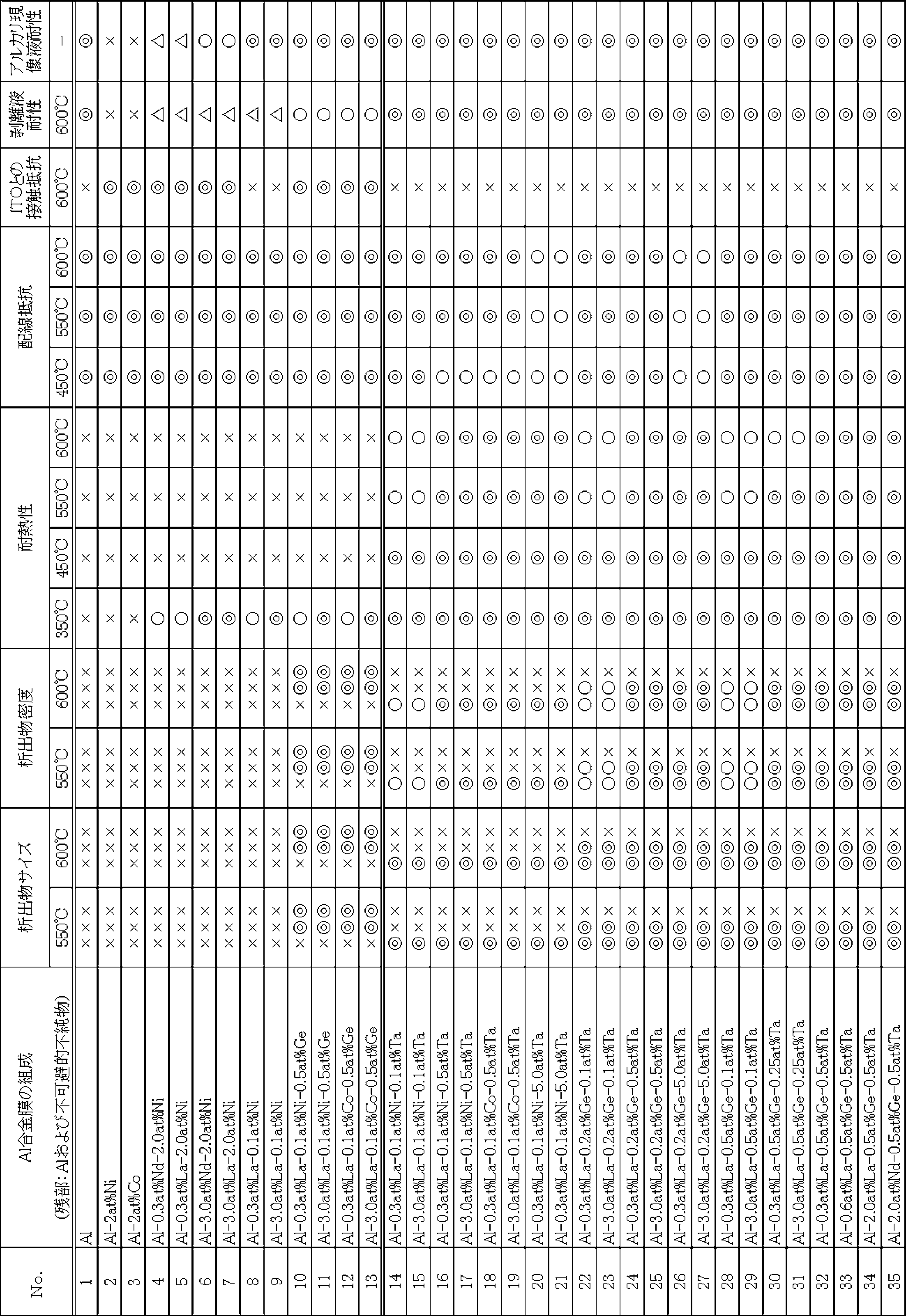


また、表6および7において、析出物サイズ(550℃/600℃)および析出物密度(550℃/600℃)が「×◎◎」(表6のNo.10~13をご参照)とは、第1の析出物のサイズおよび密度が共に「×」であるが、第2の析出物、第3の析出物のサイズおよび密度が共に「◎」を意味する。
また、表6および7において、析出物サイズ(550℃/600℃)および析出物密度(550℃/600℃)が「◎××」(表6のNo.16~21、56、57、59~62、64~69をご参照)とは、第1の析出物のサイズおよび密度が共に「◎」であるが、第2の析出物、第3の析出物のサイズおよび密度が共に「×」を意味する。なお、表6および7において、析出物サイズ(550℃/600℃)が「◎××」で、析出物密度(550℃/600℃)が「○××」(表6および7のNo.14、15、58、63をご参照)とは、第1の析出物サイズは「◎」で第1の析出物密度は「○」であり、第2の析出物、第3の析出物サイズおよび密度は共に「×」を意味する。
また、表6および7において、析出物サイズ(550℃/600℃)および析出物密度(550℃/600℃)が「◎◎×」(表6および7のNo.24~27、30~45、48~51、54、55をご参照)とは、第1の析出物、第2の析出物のサイズおよび密度が共に「◎」であるが、第3の析出物のサイズおよび密度が共に「×」を意味する。なお、表6および7において、析出物サイズ(550℃/600℃)が「◎◎×」で、析出物密度(550℃/600℃)が「○××」(表6および7のNo.22、23、28、29、46、47、52、53をご参照)とは、第1の析出物、第2の析出物サイズは「◎」で第1の析出物、第2の析出物密度は「○」であり、第3の析出物サイズおよび密度は共に「×」を意味する。 Next, consider Tables 6 and 7. In Tables 6 and 7, the precipitate size (550 ° C./600° C.) and the precipitate density (550 ° C./600° C.) are “xxx” (see Nos. 1 to 9 in Table 6). The first precipitate, the second precipitate, and the third precipitate also mean “x” in both size and density.
In Tables 6 and 7, the precipitate size (550 ° C./600° C.) and the precipitate density (550 ° C./600° C.) are “× ◎◎” (see Nos. 10 to 13 in Table 6). The size and density of the first precipitate are both “x”, but the size and density of the second precipitate and the third precipitate are both “◎”.
In Tables 6 and 7, the precipitate size (550 ° C./600° C.) and the precipitate density (550 ° C./600° C.) are “が XX” (Nos. 16 to 21, 56, 57, 59 in Table 6). ~ 62, 64 to 69) means that the size and density of the first precipitate are both “◎”, but the size and density of the second precipitate and the third precipitate are both “×”. "Means. In Tables 6 and 7, the precipitate size (550 ° C./600° C.) is “◎ xx”, and the precipitate density (550 ° C./600° C.) is “◯ XX” (No. in Tables 6 and 7). 14, 15, 58, 63) means that the first precipitate size is “◎”, the first precipitate density is “◯”, the second precipitate size, and the third precipitate size. And density both mean “x”.
In Tables 6 and 7, the precipitate size (550 ° C./600° C.) and the precipitate density (550 ° C./600° C.) are “◎◎ ×” (Nos. 24 to 27, 30 to 45 in Tables 6 and 7). 48-51, 54, and 55), the size and density of the first precipitate and the second precipitate are both “◎”, but the size and density of the third precipitate are both "X" means. In Tables 6 and 7, the precipitate size (550 ° C./600° C.) is “◎◎ ×”, and the precipitate density (550 ° C./600° C.) is “◯ XX” (No. in Tables 6 and 7). 22, 23, 28, 29, 46, 47, 52, 53) is the first precipitate, the second precipitate size is “◎”, the first precipitate, the second precipitate The density is “◯”, and the third precipitate size and density both mean “x”.
本出願は、2010年2月16日出願の日本特許出願(特願2010-031310)、2011年2月3日出願の日本特許出願(特願2011-022034)に基づくものであり、その内容はここに参照として取り込まれる。 Although this application has been described in detail and with reference to specific embodiments, it will be apparent to those skilled in the art that various changes and modifications can be made without departing from the spirit and scope of the invention.
This application is based on the Japanese patent application filed on February 16, 2010 (Japanese Patent Application No. 2010-031310) and the Japanese patent application filed on February 3, 2011 (Japanese Patent Application No. 2011-022034). Incorporated herein by reference.
本発明によれば、特に、多結晶シリコンや連続粒界結晶シリコンを半導体層に用いる薄膜トランジスタ基板を製造するプロセスにおいて、450~600℃程度の高温加熱処理、更には上記高温加熱処理が少なくとも2回行なわれる苛酷な高温環境下に曝された場合でも、半導体シリコン層のキャリア移動度が高められるため、TFTの応答速度が向上し、省エネや高速動画などに対応可能な高性能の表示装置を提供できる。 Since the first Al alloy film (Al—X group element—rare earth element alloy) according to the present invention is composed of a predetermined alloy element and the first precipitate, it is subjected to a high temperature of about 450 to 600 ° C. It is excellent in heat resistance when exposed, has good alkali corrosion resistance, and has been able to keep the electrical resistance (wiring resistance) of the film itself after high temperature treatment low. The second Al alloy film (Al-X group element-rare earth element-Ni / Co-Cu / Ge alloy) is composed of a predetermined alloy element, a first precipitate, and a second precipitate. In addition to the above characteristics, high peeling solution resistance at high temperatures and low contact resistance with the transparent conductive film can be achieved, so that direct connection with the transparent conductive film is possible.
According to the present invention, in particular, in a process for manufacturing a thin film transistor substrate using polycrystalline silicon or continuous grain boundary crystalline silicon as a semiconductor layer, the high-temperature heat treatment at about 450 to 600 ° C., and the high-temperature heat treatment is performed at least twice. Even when exposed to harsh high-temperature environments, the carrier mobility of the semiconductor silicon layer is increased, improving the TFT response speed and providing high-performance display devices that can handle energy savings and high-speed video. it can.
5 透明電極
25 走査線
26 ゲート電極
27 ゲート絶縁膜
28 ソース電極
29 ドレイン電極
30 半導体シリコン層
31 保護膜
32 低抵抗シリコン層
33 絶縁性保護膜
Claims (32)
- 表示装置に用いられるAl合金膜であって、
前記Al合金膜は、Ta、Nb、Re、Zr、W、Mo、V、Hf、Ti、CrおよびPtよりなるX群から選択される少なくとも一種の元素と、希土類元素の少なくとも一種とを含み、
前記Al合金膜に450~600℃の加熱処理を行なったとき、下記(1)の要件を満足する表示装置用Al合金膜。
(1)Alと、前記X群から選択される少なくとも一種の元素と、前記希土類元素の少なくとも一種とを含む第1の析出物について、円相当直径20nm以上の析出物が500,000個/mm2以上の密度で存在する。 An Al alloy film used in a display device,
The Al alloy film includes at least one element selected from the group X consisting of Ta, Nb, Re, Zr, W, Mo, V, Hf, Ti, Cr and Pt, and at least one rare earth element,
An Al alloy film for a display device which satisfies the following requirement (1) when the Al alloy film is subjected to a heat treatment at 450 to 600 ° C.
(1) About the 1st precipitate containing Al, at least 1 type of element selected from said X group, and at least 1 type of the said rare earth elements, 500,000 pieces / mm of precipitates with a circle equivalent diameter of 20 nm or more Present at a density of 2 or more. - 前記Al合金膜は、更にCuおよびGeのうち少なくとも一つを含み、前記Al合金膜に450~600℃の加熱処理を行なったとき、更に下記(2)の要件を満足するものである請求項1に記載の表示装置用Al合金膜。
(2)Alと、CuおよびGeのうち少なくとも一つと、前記希土類元素の少なくとも一種とを含む第2の析出物について、円相当直径200nm以上の析出物が10,000個/mm2以上の密度で存在する。 The Al alloy film further contains at least one of Cu and Ge, and when the Al alloy film is subjected to a heat treatment at 450 to 600 ° C., the following requirement (2) is further satisfied: 2. The Al alloy film for display device according to 1.
(2) About the second precipitate containing Al, at least one of Cu and Ge, and at least one kind of the rare earth element, a density of 10,000 precipitates with an equivalent circle diameter of 200 nm or more is 10,000 pieces / mm 2 or more. Exists. - 前記Al合金膜は、更にNiおよびCoのうち少なくとも1つを含み、前記Al合金膜に450~600℃の加熱処理を行なったとき、更に下記(3)の要件を満足する請求項2に記載の表示装置用Al合金膜。
(3)Alと、NiおよびCoのうち少なくとも1つと、CuおよびGeのうち少なくとも1つと、前記希土類元素の少なくとも一種とを含む第3の析出物について、円相当直径200nm以上の析出物が2,000個/mm2以上の密度で存在する。 3. The Al alloy film further includes at least one of Ni and Co, and when the Al alloy film is subjected to a heat treatment at 450 to 600 ° C., the following requirement (3) is further satisfied: Al alloy film for display devices.
(3) About the third precipitate containing Al, at least one of Ni and Co, at least one of Cu and Ge, and at least one kind of the rare earth elements, the precipitate having an equivalent circle diameter of 200 nm or more is 2 , 000 / mm 2 or more in density. - 前記第1の析出物の円相当直径は、1μm以下である請求項1に記載の表示装置用Al合金膜。 The Al alloy film for a display device according to claim 1, wherein the equivalent circle diameter of the first precipitate is 1 µm or less.
- 前記第2の析出物の円相当直径は、1μm以下である請求項2に記載の表示装置用Al合金膜。 3. The Al alloy film for a display device according to claim 2, wherein the equivalent circle diameter of the second precipitate is 1 μm or less.
- 前記第3の析出物の円相当直径は、3μm以下である請求項2に記載の表示装置用Al合金膜。 3. The Al alloy film for a display device according to claim 2, wherein an equivalent circle diameter of the third precipitate is 3 μm or less.
- 前記第3の析出物の円相当直径は、3μm以下である請求項3に記載の表示装置用Al合金膜。 The Al alloy film for a display device according to claim 3, wherein an equivalent circle diameter of the third precipitate is 3 µm or less.
- 前記X群の元素の含有量は0.1~5原子%である請求項1に記載の表示装置用Al合金膜。 2. The Al alloy film for a display device according to claim 1, wherein the content of the group X element is 0.1 to 5 atomic%.
- 前記希土類元素の含有量は0.1~4原子%である請求項1に記載の表示装置用Al合金膜。 2. The Al alloy film for a display device according to claim 1, wherein a content of the rare earth element is 0.1 to 4 atomic%.
- 前記CuおよびGeのうち少なくとも1つの含有量は0.1~2原子%である請求項2に記載の表示装置用Al合金膜。 3. The Al alloy film for a display device according to claim 2, wherein the content of at least one of Cu and Ge is 0.1 to 2 atomic%.
- 前記NiおよびCoのうち少なくとも1つの含有量は0.1~3原子%である請求項3に記載の表示装置用Al合金膜。 4. The Al alloy film for a display device according to claim 3, wherein the content of at least one of Ni and Co is 0.1 to 3 atomic%.
- 前記加熱処理は、500~600℃である請求項1に記載の表示装置用Al合金膜。 The Al alloy film for a display device according to claim 1, wherein the heat treatment is performed at 500 to 600 ° C.
- 前記加熱処理は、500~600℃である請求項2に記載の表示装置用Al合金膜。 The Al alloy film for a display device according to claim 2, wherein the heat treatment is performed at 500 to 600 ° C.
- 前記加熱処理は、500~600℃である請求項3に記載の表示装置用Al合金膜。 The Al alloy film for a display device according to claim 3, wherein the heat treatment is performed at 500 to 600 ° C.
- 前記加熱処理は、少なくとも2回実施されるものである請求項1に記載の表示装置用Al合金膜。 The Al alloy film for a display device according to claim 1, wherein the heat treatment is performed at least twice.
- 前記加熱処理は、少なくとも2回実施されるものである請求項2に記載の表示装置用Al合金膜。 The Al alloy film for a display device according to claim 2, wherein the heat treatment is performed at least twice.
- 前記加熱処理は、少なくとも2回実施されるものである請求項3に記載の表示装置用Al合金膜。 4. The Al alloy film for a display device according to claim 3, wherein the heat treatment is performed at least twice.
- 前記Al合金膜は、透明導電膜と直接接続されるものである請求項2に記載の表示装置用Al合金膜。 3. The Al alloy film for a display device according to claim 2, wherein the Al alloy film is directly connected to a transparent conductive film.
- 前記Al合金膜は、透明導電膜と直接接続されるものである請求項3に記載の表示装置用Al合金膜。 4. The Al alloy film for a display device according to claim 3, wherein the Al alloy film is directly connected to a transparent conductive film.
- 前記Al合金膜は、Mo、Ti、W、およびCrよりなる群から選択される少なくとも一種の元素を含む膜を介して透明導電膜と接続されるものである請求項1に記載の表示装置用Al合金膜。 The display device according to claim 1, wherein the Al alloy film is connected to the transparent conductive film through a film containing at least one element selected from the group consisting of Mo, Ti, W, and Cr. Al alloy film.
- 前記Al合金膜は、Mo、Ti、W、およびCrよりなる群から選択される少なくとも一種の元素を含む膜を介して透明導電膜と接続されるものである請求項2に記載の表示装置用Al合金膜。 The display device according to claim 2, wherein the Al alloy film is connected to the transparent conductive film through a film containing at least one element selected from the group consisting of Mo, Ti, W, and Cr. Al alloy film.
- 前記Al合金膜は、Mo、Ti、W、およびCrよりなる群から選択される少なくとも一種の元素を含む膜を介して透明導電膜と接続されるものである請求項3に記載の表示装置用Al合金膜。 4. The display device according to claim 3, wherein the Al alloy film is connected to the transparent conductive film through a film containing at least one element selected from the group consisting of Mo, Ti, W, and Cr. Al alloy film.
- Ta、Nb、Re、Zr、W、Mo、V、Hf、Ti、CrおよびPtよりなるX群から選択される少なくとも一種の元素を0.1~5原子%、および希土類元素の少なくとも一種を0.1~4原子%を含み、残部:Alおよび不可避的不純物であるスパッタリングターゲット。 0.1 to 5 atomic% of at least one element selected from X group consisting of Ta, Nb, Re, Zr, W, Mo, V, Hf, Ti, Cr and Pt, and at least one element of rare earth elements to 0 A sputtering target containing 1 to 4 atomic%, the balance: Al and inevitable impurities.
- 更に、CuおよびGeのうち少なくとも1つを0.1~2原子%含む請求項23に記載のスパッタリングターゲット。 The sputtering target according to claim 23, further comprising 0.1 to 2 atomic% of at least one of Cu and Ge.
- 更に、NiおよびCoのうち少なくとも1つを0.1~3原子%含む請求項24に記載のスパッタリングターゲット。 The sputtering target according to claim 24, further comprising 0.1 to 3 atomic% of at least one of Ni and Co.
- 請求項1~22のいずれか1つに記載の表示装置用Al合金膜を備えた表示装置。 A display device comprising the Al alloy film for a display device according to any one of claims 1 to 22.
- 請求項1~22のいずれか1つに記載の表示装置用Al合金膜を備えた液晶ディスプレイ。 A liquid crystal display comprising the Al alloy film for a display device according to any one of claims 1 to 22.
- 請求項1~22のいずれか1つに記載の表示装置用Al合金膜を備えた有機ELディスプレイ。 An organic EL display comprising the Al alloy film for a display device according to any one of claims 1 to 22.
- 請求項1~22のいずれか1つに記載の表示装置用Al合金膜を備えたフィールドエミッションディスプレイ。 A field emission display comprising the Al alloy film for a display device according to any one of claims 1 to 22.
- 請求項1~22のいずれか1つに記載の表示装置用Al合金膜を備えた蛍光真空管。 A fluorescent vacuum tube comprising the Al alloy film for a display device according to any one of claims 1 to 22.
- 請求項1~22のいずれか1つに記載の表示装置用Al合金膜を備えたプラズマディスプレイ。 A plasma display comprising the Al alloy film for a display device according to any one of claims 1 to 22.
- 請求項1~22のいずれか1つに記載の表示装置用Al合金膜を備えた無機ELディスプレイ。 An inorganic EL display comprising the Al alloy film for a display device according to any one of claims 1 to 22.
Priority Applications (3)
| Application Number | Priority Date | Filing Date | Title |
|---|---|---|---|
| US13/576,053 US20120301732A1 (en) | 2010-02-16 | 2011-02-16 | Al alloy film for use in display device |
| CN201180008362.XA CN102741449B (en) | 2010-02-16 | 2011-02-16 | Al alloy film for display device |
| KR1020127021341A KR101428349B1 (en) | 2010-02-16 | 2011-02-16 | Al alloy film for display device |
Applications Claiming Priority (2)
| Application Number | Priority Date | Filing Date | Title |
|---|---|---|---|
| JP2010-031310 | 2010-02-16 | ||
| JP2010031310 | 2010-02-16 |
Publications (1)
| Publication Number | Publication Date |
|---|---|
| WO2011102396A1 true WO2011102396A1 (en) | 2011-08-25 |
Family
ID=44482981
Family Applications (1)
| Application Number | Title | Priority Date | Filing Date |
|---|---|---|---|
| PCT/JP2011/053300 WO2011102396A1 (en) | 2010-02-16 | 2011-02-16 | Al alloy film for display device |
Country Status (6)
| Country | Link |
|---|---|
| US (1) | US20120301732A1 (en) |
| JP (1) | JP5179604B2 (en) |
| KR (1) | KR101428349B1 (en) |
| CN (1) | CN102741449B (en) |
| TW (1) | TWI432589B (en) |
| WO (1) | WO2011102396A1 (en) |
Cited By (2)
| Publication number | Priority date | Publication date | Assignee | Title |
|---|---|---|---|---|
| WO2013047095A1 (en) * | 2011-09-28 | 2013-04-04 | 株式会社神戸製鋼所 | Wiring structure for display device |
| JP2014535159A (en) * | 2011-09-29 | 2014-12-25 | インテル・コーポレーション | Positive metal-containing layer for semiconductor applications |
Families Citing this family (9)
| Publication number | Priority date | Publication date | Assignee | Title |
|---|---|---|---|---|
| JP5524905B2 (en) * | 2011-05-17 | 2014-06-18 | 株式会社神戸製鋼所 | Al alloy film for power semiconductor devices |
| JP5805708B2 (en) * | 2013-06-05 | 2015-11-04 | 株式会社神戸製鋼所 | Wiring film for touch panel sensor and touch panel sensor |
| AT14576U1 (en) | 2014-08-20 | 2016-01-15 | Plansee Se | Metallization for a thin film device, method of making the same and sputtering target |
| JP6228631B1 (en) * | 2016-06-07 | 2017-11-08 | 株式会社コベルコ科研 | Al alloy sputtering target |
| JP7053290B2 (en) * | 2018-02-05 | 2022-04-12 | 株式会社神戸製鋼所 | Reflective anode electrode for organic EL display |
| WO2020003666A1 (en) * | 2018-06-28 | 2020-01-02 | 株式会社アルバック | Aluminum alloy target and method for producing same |
| WO2020003667A1 (en) * | 2018-06-28 | 2020-01-02 | 株式会社アルバック | Aluminum alloy film, method for producing same, and thin film transistor |
| CN110468312B (en) * | 2019-09-26 | 2021-03-23 | 常州斯威克新材料科技有限公司 | Corrosion-resistant aluminum alloy target material for photovoltaic reflective film, preparation method of corrosion-resistant aluminum alloy target material and aluminum alloy film |
| CN113832372B (en) * | 2021-08-19 | 2022-10-21 | 马鞍山市申马机械制造有限公司 | Alloy powder, and preparation method, application and application method thereof |
Citations (4)
| Publication number | Priority date | Publication date | Assignee | Title |
|---|---|---|---|---|
| JP2000294556A (en) * | 1999-04-05 | 2000-10-20 | Hitachi Metals Ltd | Aluminum alloy wiring film excellent in dry etching and target for aluminum alloy wiring film formation |
| JP2005141250A (en) * | 2001-03-29 | 2005-06-02 | Nec Lcd Technologies Ltd | Method for manufacturing liquid crystal display device |
| JP2008098611A (en) * | 2006-09-15 | 2008-04-24 | Kobe Steel Ltd | Display device |
| JP2009175719A (en) * | 2007-12-26 | 2009-08-06 | Kobe Steel Ltd | Reflecting electrode, display device, and method of manufacturing display device |
Family Cites Families (15)
| Publication number | Priority date | Publication date | Assignee | Title |
|---|---|---|---|---|
| JP3382031B2 (en) * | 1993-11-16 | 2003-03-04 | 株式会社東芝 | Method for manufacturing semiconductor device |
| JP3212024B2 (en) * | 1996-11-14 | 2001-09-25 | 日立金属株式会社 | Target material for Al-based sputtering and method for producing the same |
| WO1999034028A1 (en) * | 1997-12-24 | 1999-07-08 | Kabushiki Kaisha Toshiba | SPUTTERING TARGET, Al INTERCONNECTION FILM, AND ELECTRONIC COMPONENT |
| JPH11293454A (en) * | 1998-04-14 | 1999-10-26 | Hitachi Metals Ltd | Target material for aluminum series sputtering and its production |
| JP2001312840A (en) * | 2000-04-28 | 2001-11-09 | Tosoh Corp | Surface readout type optical recording medium |
| JP3908552B2 (en) * | 2001-03-29 | 2007-04-25 | Nec液晶テクノロジー株式会社 | Liquid crystal display device and manufacturing method thereof |
| JP4783525B2 (en) * | 2001-08-31 | 2011-09-28 | 株式会社アルバック | Thin film aluminum alloy and sputtering target for forming thin film aluminum alloy |
| JP3940385B2 (en) * | 2002-12-19 | 2007-07-04 | 株式会社神戸製鋼所 | Display device and manufacturing method thereof |
| JP4579709B2 (en) * | 2005-02-15 | 2010-11-10 | 株式会社神戸製鋼所 | Al-Ni-rare earth alloy sputtering target |
| JP4117001B2 (en) * | 2005-02-17 | 2008-07-09 | 株式会社神戸製鋼所 | Thin film transistor substrate, display device, and sputtering target for display device |
| JP4117002B2 (en) * | 2005-12-02 | 2008-07-09 | 株式会社神戸製鋼所 | Thin film transistor substrate and display device |
| JP4170367B2 (en) * | 2006-11-30 | 2008-10-22 | 株式会社神戸製鋼所 | Al alloy film for display device, display device, and sputtering target |
| US20110008640A1 (en) * | 2008-03-31 | 2011-01-13 | Kabushiki Kaisha Kobe Seiko Sho (Kobe Steel Ltd.) | Display device, process for producing the display device, and sputtering target |
| US20110198602A1 (en) * | 2008-11-05 | 2011-08-18 | Kabushiki Kaisha Kobe Seiko Sho (Kobe Steel, Ltd.) | Aluminum alloy film for display device, display device, and sputtering target |
| JP2010134458A (en) * | 2008-11-05 | 2010-06-17 | Kobe Steel Ltd | Al alloy film for display, display and sputtering target |
-
2011
- 2011-02-03 JP JP2011022034A patent/JP5179604B2/en not_active Expired - Fee Related
- 2011-02-16 CN CN201180008362.XA patent/CN102741449B/en not_active Expired - Fee Related
- 2011-02-16 US US13/576,053 patent/US20120301732A1/en not_active Abandoned
- 2011-02-16 TW TW100105081A patent/TWI432589B/en not_active IP Right Cessation
- 2011-02-16 WO PCT/JP2011/053300 patent/WO2011102396A1/en active Application Filing
- 2011-02-16 KR KR1020127021341A patent/KR101428349B1/en active IP Right Grant
Patent Citations (4)
| Publication number | Priority date | Publication date | Assignee | Title |
|---|---|---|---|---|
| JP2000294556A (en) * | 1999-04-05 | 2000-10-20 | Hitachi Metals Ltd | Aluminum alloy wiring film excellent in dry etching and target for aluminum alloy wiring film formation |
| JP2005141250A (en) * | 2001-03-29 | 2005-06-02 | Nec Lcd Technologies Ltd | Method for manufacturing liquid crystal display device |
| JP2008098611A (en) * | 2006-09-15 | 2008-04-24 | Kobe Steel Ltd | Display device |
| JP2009175719A (en) * | 2007-12-26 | 2009-08-06 | Kobe Steel Ltd | Reflecting electrode, display device, and method of manufacturing display device |
Cited By (6)
| Publication number | Priority date | Publication date | Assignee | Title |
|---|---|---|---|---|
| WO2013047095A1 (en) * | 2011-09-28 | 2013-04-04 | 株式会社神戸製鋼所 | Wiring structure for display device |
| JP2013084907A (en) * | 2011-09-28 | 2013-05-09 | Kobe Steel Ltd | Wiring structure for display device |
| CN103782374A (en) * | 2011-09-28 | 2014-05-07 | 株式会社神户制钢所 | Wiring structure for display device |
| US10365520B2 (en) | 2011-09-28 | 2019-07-30 | Kobe Steel, Ltd. | Wiring structure for display device |
| JP2014535159A (en) * | 2011-09-29 | 2014-12-25 | インテル・コーポレーション | Positive metal-containing layer for semiconductor applications |
| US9390932B2 (en) | 2011-09-29 | 2016-07-12 | Intel Corporation | Electropositive metal containing layers for semiconductor applications |
Also Published As
| Publication number | Publication date |
|---|---|
| CN102741449B (en) | 2015-04-29 |
| CN102741449A (en) | 2012-10-17 |
| JP5179604B2 (en) | 2013-04-10 |
| US20120301732A1 (en) | 2012-11-29 |
| KR20120112796A (en) | 2012-10-11 |
| KR101428349B1 (en) | 2014-08-07 |
| TWI432589B (en) | 2014-04-01 |
| TW201300552A (en) | 2013-01-01 |
| JP2011190531A (en) | 2011-09-29 |
Similar Documents
| Publication | Publication Date | Title |
|---|---|---|
| JP5179604B2 (en) | Al alloy film for display devices | |
| TWI356498B (en) | ||
| TWI437697B (en) | Wiring structure and a display device having a wiring structure | |
| WO2010053135A1 (en) | Al alloy film for display device, display device and sputtering target | |
| CN101918888B (en) | Display device, process for producing the display device, and sputtering target | |
| WO2012043490A1 (en) | Al alloy film, wiring structure having al alloy film, and sputtering target used in producing al alloy film | |
| JP2009280911A (en) | Aluminum alloy film for display device, display device and sputtering target | |
| WO2012118039A1 (en) | Al alloy film for display devices or semiconductor devices, display device or semiconductor device equipped with al alloy film, and sputtering target | |
| WO2013047095A1 (en) | Wiring structure for display device | |
| TW201543555A (en) | Wiring film for flat panel display | |
| JP5491947B2 (en) | Al alloy film for display devices | |
| JP2012189725A (en) | WIRING FILM AND ELECTRODE USING Ti ALLOY BARRIER METAL AND Ti ALLOY SPUTTERING TARGET | |
| JP5357515B2 (en) | Al alloy film for display device, display device and sputtering target | |
| JP2010238800A (en) | Al ALLOY FILM FOR DISPLAY, THIN FILM TRANSISTOR SUBSTRATE AND DISPLAY | |
| JP6002280B2 (en) | Al alloy film for display devices or semiconductor devices | |
| JP2012189726A (en) | WIRING FILM AND ELECTRODE USING Ti ALLOY BARRIER METAL AND Ti ALLOY SPUTTERING TARGET | |
| JP4188299B2 (en) | Ag-based alloy wiring electrode film for flat panel display, Ag-based alloy sputtering target, and flat panel display | |
| JP2011017944A (en) | Aluminum alloy film for display device, display device, and aluminum alloy sputtering target | |
| JP2017033963A (en) | Thin film transistor | |
| JP5368806B2 (en) | Al alloy film for display device and display device | |
| JP2013224486A (en) | Al ALLOY FILM FOR DISPLAY DEVICE AND DISPLAY DEVICE | |
| TW201030819A (en) | Al alloy film for display device, thin film transistor substrate, method for manufacturing same, and display device |
Legal Events
| Date | Code | Title | Description |
|---|---|---|---|
| WWE | Wipo information: entry into national phase |
Ref document number: 201180008362.X Country of ref document: CN |
|
| 121 | Ep: the epo has been informed by wipo that ep was designated in this application |
Ref document number: 11744682 Country of ref document: EP Kind code of ref document: A1 |
|
| WWE | Wipo information: entry into national phase |
Ref document number: 13576053 Country of ref document: US |
|
| ENP | Entry into the national phase |
Ref document number: 20127021341 Country of ref document: KR Kind code of ref document: A |
|
| NENP | Non-entry into the national phase |
Ref country code: DE |
|
| 122 | Ep: pct application non-entry in european phase |
Ref document number: 11744682 Country of ref document: EP Kind code of ref document: A1 |