JP3908552B2 - Liquid crystal display device and manufacturing method thereof - Google Patents
Liquid crystal display device and manufacturing method thereof Download PDFInfo
- Publication number
- JP3908552B2 JP3908552B2 JP2002030472A JP2002030472A JP3908552B2 JP 3908552 B2 JP3908552 B2 JP 3908552B2 JP 2002030472 A JP2002030472 A JP 2002030472A JP 2002030472 A JP2002030472 A JP 2002030472A JP 3908552 B2 JP3908552 B2 JP 3908552B2
- Authority
- JP
- Japan
- Prior art keywords
- film
- liquid crystal
- crystal display
- display device
- insulating film
- Prior art date
- Legal status (The legal status is an assumption and is not a legal conclusion. Google has not performed a legal analysis and makes no representation as to the accuracy of the status listed.)
- Expired - Lifetime
Links
- 239000004973 liquid crystal related substance Substances 0.000 title claims abstract description 101
- 238000004519 manufacturing process Methods 0.000 title description 32
- 239000000758 substrate Substances 0.000 claims abstract description 125
- 239000013078 crystal Substances 0.000 claims description 3
- 229910000583 Nd alloy Inorganic materials 0.000 abstract description 41
- 230000003287 optical effect Effects 0.000 abstract description 7
- 229910052779 Neodymium Inorganic materials 0.000 abstract description 5
- QEFYFXOXNSNQGX-UHFFFAOYSA-N neodymium atom Chemical compound [Nd] QEFYFXOXNSNQGX-UHFFFAOYSA-N 0.000 abstract description 2
- UBSJOWMHLJZVDJ-UHFFFAOYSA-N aluminum neodymium Chemical compound [Al].[Nd] UBSJOWMHLJZVDJ-UHFFFAOYSA-N 0.000 abstract 1
- 239000011295 pitch Substances 0.000 abstract 1
- 239000010408 film Substances 0.000 description 380
- 238000000034 method Methods 0.000 description 73
- 230000015572 biosynthetic process Effects 0.000 description 60
- 229910052751 metal Inorganic materials 0.000 description 59
- 239000002184 metal Substances 0.000 description 59
- 230000008569 process Effects 0.000 description 47
- 239000010410 layer Substances 0.000 description 34
- 238000000059 patterning Methods 0.000 description 31
- 238000002161 passivation Methods 0.000 description 27
- 238000010438 heat treatment Methods 0.000 description 24
- 238000002310 reflectometry Methods 0.000 description 22
- 229910021417 amorphous silicon Inorganic materials 0.000 description 21
- 239000011229 interlayer Substances 0.000 description 13
- 238000000206 photolithography Methods 0.000 description 13
- 229920005989 resin Polymers 0.000 description 12
- 239000011347 resin Substances 0.000 description 12
- 239000011651 chromium Substances 0.000 description 10
- 238000004544 sputter deposition Methods 0.000 description 10
- 238000004383 yellowing Methods 0.000 description 10
- 238000006243 chemical reaction Methods 0.000 description 9
- 239000000463 material Substances 0.000 description 9
- 238000002834 transmittance Methods 0.000 description 9
- 229910052782 aluminium Inorganic materials 0.000 description 8
- 230000018109 developmental process Effects 0.000 description 8
- 239000011159 matrix material Substances 0.000 description 8
- 229910052750 molybdenum Inorganic materials 0.000 description 8
- 239000003566 sealing material Substances 0.000 description 8
- QTBSBXVTEAMEQO-UHFFFAOYSA-N acetic acid Substances CC(O)=O QTBSBXVTEAMEQO-UHFFFAOYSA-N 0.000 description 7
- 239000011248 coating agent Substances 0.000 description 7
- 238000000576 coating method Methods 0.000 description 7
- 239000011521 glass Substances 0.000 description 7
- 229910000838 Al alloy Inorganic materials 0.000 description 6
- 229910045601 alloy Inorganic materials 0.000 description 6
- 239000000956 alloy Substances 0.000 description 6
- 229920003986 novolac Polymers 0.000 description 6
- 229910052581 Si3N4 Inorganic materials 0.000 description 5
- 229910052804 chromium Inorganic materials 0.000 description 5
- 230000003247 decreasing effect Effects 0.000 description 5
- 238000010586 diagram Methods 0.000 description 5
- 238000005268 plasma chemical vapour deposition Methods 0.000 description 5
- HQVNEWCFYHHQES-UHFFFAOYSA-N silicon nitride Chemical compound N12[Si]34N5[Si]62N3[Si]51N64 HQVNEWCFYHHQES-UHFFFAOYSA-N 0.000 description 5
- 239000010409 thin film Substances 0.000 description 5
- SECXISVLQFMRJM-UHFFFAOYSA-N N-Methylpyrrolidone Chemical compound CN1CCCC1=O SECXISVLQFMRJM-UHFFFAOYSA-N 0.000 description 4
- 206010034972 Photosensitivity reaction Diseases 0.000 description 4
- 230000009471 action Effects 0.000 description 4
- 239000002585 base Substances 0.000 description 4
- 238000005530 etching Methods 0.000 description 4
- 230000036211 photosensitivity Effects 0.000 description 4
- 239000004033 plastic Substances 0.000 description 4
- 229920001721 polyimide Polymers 0.000 description 4
- 239000004065 semiconductor Substances 0.000 description 4
- 239000010936 titanium Substances 0.000 description 4
- 239000004925 Acrylic resin Substances 0.000 description 3
- MUBZPKHOEPUJKR-UHFFFAOYSA-N Oxalic acid Chemical compound OC(=O)C(O)=O MUBZPKHOEPUJKR-UHFFFAOYSA-N 0.000 description 3
- 230000004888 barrier function Effects 0.000 description 3
- 230000007423 decrease Effects 0.000 description 3
- 230000000694 effects Effects 0.000 description 3
- 230000031700 light absorption Effects 0.000 description 3
- 239000002245 particle Substances 0.000 description 3
- BASFCYQUMIYNBI-UHFFFAOYSA-N platinum Chemical compound [Pt] BASFCYQUMIYNBI-UHFFFAOYSA-N 0.000 description 3
- 238000007639 printing Methods 0.000 description 3
- 230000002829 reductive effect Effects 0.000 description 3
- 230000002441 reversible effect Effects 0.000 description 3
- 125000006850 spacer group Chemical group 0.000 description 3
- 239000000126 substance Substances 0.000 description 3
- 229910052719 titanium Inorganic materials 0.000 description 3
- 229920000178 Acrylic resin Polymers 0.000 description 2
- 229910001316 Ag alloy Inorganic materials 0.000 description 2
- NBIIXXVUZAFLBC-UHFFFAOYSA-N Phosphoric acid Chemical compound OP(O)(O)=O NBIIXXVUZAFLBC-UHFFFAOYSA-N 0.000 description 2
- 239000004642 Polyimide Substances 0.000 description 2
- 229910004205 SiNX Inorganic materials 0.000 description 2
- VYPSYNLAJGMNEJ-UHFFFAOYSA-N Silicium dioxide Chemical compound O=[Si]=O VYPSYNLAJGMNEJ-UHFFFAOYSA-N 0.000 description 2
- BQCADISMDOOEFD-UHFFFAOYSA-N Silver Chemical compound [Ag] BQCADISMDOOEFD-UHFFFAOYSA-N 0.000 description 2
- 206010040844 Skin exfoliation Diseases 0.000 description 2
- 230000002411 adverse Effects 0.000 description 2
- 239000003513 alkali Substances 0.000 description 2
- 230000008859 change Effects 0.000 description 2
- 230000007547 defect Effects 0.000 description 2
- 238000010304 firing Methods 0.000 description 2
- 238000009413 insulation Methods 0.000 description 2
- 239000000203 mixture Substances 0.000 description 2
- 230000003071 parasitic effect Effects 0.000 description 2
- 229910021420 polycrystalline silicon Inorganic materials 0.000 description 2
- 239000009719 polyimide resin Substances 0.000 description 2
- 230000007261 regionalization Effects 0.000 description 2
- 229910052709 silver Inorganic materials 0.000 description 2
- 239000004332 silver Substances 0.000 description 2
- 229910018575 Al—Ti Inorganic materials 0.000 description 1
- VYZAMTAEIAYCRO-UHFFFAOYSA-N Chromium Chemical compound [Cr] VYZAMTAEIAYCRO-UHFFFAOYSA-N 0.000 description 1
- 229910021578 Iron(III) chloride Inorganic materials 0.000 description 1
- 229910001182 Mo alloy Inorganic materials 0.000 description 1
- ZOKXTWBITQBERF-UHFFFAOYSA-N Molybdenum Chemical compound [Mo] ZOKXTWBITQBERF-UHFFFAOYSA-N 0.000 description 1
- GRYLNZFGIOXLOG-UHFFFAOYSA-N Nitric acid Chemical compound O[N+]([O-])=O GRYLNZFGIOXLOG-UHFFFAOYSA-N 0.000 description 1
- 229910004298 SiO 2 Inorganic materials 0.000 description 1
- RTAQQCXQSZGOHL-UHFFFAOYSA-N Titanium Chemical compound [Ti] RTAQQCXQSZGOHL-UHFFFAOYSA-N 0.000 description 1
- 238000010521 absorption reaction Methods 0.000 description 1
- 239000002253 acid Substances 0.000 description 1
- 239000000853 adhesive Substances 0.000 description 1
- 230000001070 adhesive effect Effects 0.000 description 1
- XAGFODPZIPBFFR-UHFFFAOYSA-N aluminium Chemical compound [Al] XAGFODPZIPBFFR-UHFFFAOYSA-N 0.000 description 1
- 229910000147 aluminium phosphate Inorganic materials 0.000 description 1
- QZPSXPBJTPJTSZ-UHFFFAOYSA-N aqua regia Chemical compound Cl.O[N+]([O-])=O QZPSXPBJTPJTSZ-UHFFFAOYSA-N 0.000 description 1
- 239000011324 bead Substances 0.000 description 1
- 230000005540 biological transmission Effects 0.000 description 1
- 239000003990 capacitor Substances 0.000 description 1
- 239000000919 ceramic Substances 0.000 description 1
- 239000003086 colorant Substances 0.000 description 1
- 238000004040 coloring Methods 0.000 description 1
- 238000009833 condensation Methods 0.000 description 1
- 230000005494 condensation Effects 0.000 description 1
- 238000011109 contamination Methods 0.000 description 1
- 238000001312 dry etching Methods 0.000 description 1
- 238000001035 drying Methods 0.000 description 1
- 230000005684 electric field Effects 0.000 description 1
- 239000007772 electrode material Substances 0.000 description 1
- 239000003822 epoxy resin Substances 0.000 description 1
- 238000002474 experimental method Methods 0.000 description 1
- 238000011049 filling Methods 0.000 description 1
- -1 for example Substances 0.000 description 1
- 230000001771 impaired effect Effects 0.000 description 1
- 239000012535 impurity Substances 0.000 description 1
- 238000002347 injection Methods 0.000 description 1
- 239000007924 injection Substances 0.000 description 1
- 238000005468 ion implantation Methods 0.000 description 1
- 150000002500 ions Chemical class 0.000 description 1
- RBTARNINKXHZNM-UHFFFAOYSA-K iron trichloride Chemical compound Cl[Fe](Cl)Cl RBTARNINKXHZNM-UHFFFAOYSA-K 0.000 description 1
- 230000000670 limiting effect Effects 0.000 description 1
- 239000007788 liquid Substances 0.000 description 1
- 239000007791 liquid phase Substances 0.000 description 1
- 238000001459 lithography Methods 0.000 description 1
- 230000007257 malfunction Effects 0.000 description 1
- 230000007246 mechanism Effects 0.000 description 1
- 238000002844 melting Methods 0.000 description 1
- 230000008018 melting Effects 0.000 description 1
- 238000010309 melting process Methods 0.000 description 1
- 150000002739 metals Chemical class 0.000 description 1
- 238000002156 mixing Methods 0.000 description 1
- 239000011733 molybdenum Substances 0.000 description 1
- 230000000877 morphologic effect Effects 0.000 description 1
- 229910017604 nitric acid Inorganic materials 0.000 description 1
- 238000010943 off-gassing Methods 0.000 description 1
- 235000006408 oxalic acid Nutrition 0.000 description 1
- 230000036961 partial effect Effects 0.000 description 1
- 230000002093 peripheral effect Effects 0.000 description 1
- 239000012071 phase Substances 0.000 description 1
- 229920002120 photoresistant polymer Polymers 0.000 description 1
- 229910052697 platinum Inorganic materials 0.000 description 1
- 229920000647 polyepoxide Polymers 0.000 description 1
- 238000006116 polymerization reaction Methods 0.000 description 1
- 229920005591 polysilicon Polymers 0.000 description 1
- 230000001681 protective effect Effects 0.000 description 1
- 230000009467 reduction Effects 0.000 description 1
- 239000003870 refractory metal Substances 0.000 description 1
- 230000004044 response Effects 0.000 description 1
- LIVNPJMFVYWSIS-UHFFFAOYSA-N silicon monoxide Chemical compound [Si-]#[O+] LIVNPJMFVYWSIS-UHFFFAOYSA-N 0.000 description 1
- 229910052814 silicon oxide Inorganic materials 0.000 description 1
- 238000009751 slip forming Methods 0.000 description 1
- 238000002791 soaking Methods 0.000 description 1
- 239000000243 solution Substances 0.000 description 1
- 238000003860 storage Methods 0.000 description 1
- 238000007740 vapor deposition Methods 0.000 description 1
- 238000001039 wet etching Methods 0.000 description 1
- 230000037303 wrinkles Effects 0.000 description 1
Images


Classifications
-
- G—PHYSICS
- G02—OPTICS
- G02F—OPTICAL DEVICES OR ARRANGEMENTS FOR THE CONTROL OF LIGHT BY MODIFICATION OF THE OPTICAL PROPERTIES OF THE MEDIA OF THE ELEMENTS INVOLVED THEREIN; NON-LINEAR OPTICS; FREQUENCY-CHANGING OF LIGHT; OPTICAL LOGIC ELEMENTS; OPTICAL ANALOGUE/DIGITAL CONVERTERS
- G02F1/00—Devices or arrangements for the control of the intensity, colour, phase, polarisation or direction of light arriving from an independent light source, e.g. switching, gating or modulating; Non-linear optics
- G02F1/01—Devices or arrangements for the control of the intensity, colour, phase, polarisation or direction of light arriving from an independent light source, e.g. switching, gating or modulating; Non-linear optics for the control of the intensity, phase, polarisation or colour
- G02F1/13—Devices or arrangements for the control of the intensity, colour, phase, polarisation or direction of light arriving from an independent light source, e.g. switching, gating or modulating; Non-linear optics for the control of the intensity, phase, polarisation or colour based on liquid crystals, e.g. single liquid crystal display cells
- G02F1/133—Constructional arrangements; Operation of liquid crystal cells; Circuit arrangements
- G02F1/1333—Constructional arrangements; Manufacturing methods
- G02F1/1335—Structural association of cells with optical devices, e.g. polarisers or reflectors
- G02F1/133553—Reflecting elements
-
- G—PHYSICS
- G02—OPTICS
- G02F—OPTICAL DEVICES OR ARRANGEMENTS FOR THE CONTROL OF LIGHT BY MODIFICATION OF THE OPTICAL PROPERTIES OF THE MEDIA OF THE ELEMENTS INVOLVED THEREIN; NON-LINEAR OPTICS; FREQUENCY-CHANGING OF LIGHT; OPTICAL LOGIC ELEMENTS; OPTICAL ANALOGUE/DIGITAL CONVERTERS
- G02F1/00—Devices or arrangements for the control of the intensity, colour, phase, polarisation or direction of light arriving from an independent light source, e.g. switching, gating or modulating; Non-linear optics
- G02F1/01—Devices or arrangements for the control of the intensity, colour, phase, polarisation or direction of light arriving from an independent light source, e.g. switching, gating or modulating; Non-linear optics for the control of the intensity, phase, polarisation or colour
- G02F1/13—Devices or arrangements for the control of the intensity, colour, phase, polarisation or direction of light arriving from an independent light source, e.g. switching, gating or modulating; Non-linear optics for the control of the intensity, phase, polarisation or colour based on liquid crystals, e.g. single liquid crystal display cells
- G02F1/133—Constructional arrangements; Operation of liquid crystal cells; Circuit arrangements
- G02F1/1333—Constructional arrangements; Manufacturing methods
- G02F1/1335—Structural association of cells with optical devices, e.g. polarisers or reflectors
-
- C—CHEMISTRY; METALLURGY
- C09—DYES; PAINTS; POLISHES; NATURAL RESINS; ADHESIVES; COMPOSITIONS NOT OTHERWISE PROVIDED FOR; APPLICATIONS OF MATERIALS NOT OTHERWISE PROVIDED FOR
- C09K—MATERIALS FOR MISCELLANEOUS APPLICATIONS, NOT PROVIDED FOR ELSEWHERE
- C09K2323/00—Functional layers of liquid crystal optical display excluding electroactive liquid crystal layer characterised by chemical composition
- C09K2323/03—Viewing layer characterised by chemical composition
-
- G—PHYSICS
- G02—OPTICS
- G02F—OPTICAL DEVICES OR ARRANGEMENTS FOR THE CONTROL OF LIGHT BY MODIFICATION OF THE OPTICAL PROPERTIES OF THE MEDIA OF THE ELEMENTS INVOLVED THEREIN; NON-LINEAR OPTICS; FREQUENCY-CHANGING OF LIGHT; OPTICAL LOGIC ELEMENTS; OPTICAL ANALOGUE/DIGITAL CONVERTERS
- G02F1/00—Devices or arrangements for the control of the intensity, colour, phase, polarisation or direction of light arriving from an independent light source, e.g. switching, gating or modulating; Non-linear optics
- G02F1/01—Devices or arrangements for the control of the intensity, colour, phase, polarisation or direction of light arriving from an independent light source, e.g. switching, gating or modulating; Non-linear optics for the control of the intensity, phase, polarisation or colour
- G02F1/13—Devices or arrangements for the control of the intensity, colour, phase, polarisation or direction of light arriving from an independent light source, e.g. switching, gating or modulating; Non-linear optics for the control of the intensity, phase, polarisation or colour based on liquid crystals, e.g. single liquid crystal display cells
- G02F1/133—Constructional arrangements; Operation of liquid crystal cells; Circuit arrangements
- G02F1/1333—Constructional arrangements; Manufacturing methods
- G02F1/1335—Structural association of cells with optical devices, e.g. polarisers or reflectors
- G02F1/133504—Diffusing, scattering, diffracting elements
-
- G—PHYSICS
- G02—OPTICS
- G02F—OPTICAL DEVICES OR ARRANGEMENTS FOR THE CONTROL OF LIGHT BY MODIFICATION OF THE OPTICAL PROPERTIES OF THE MEDIA OF THE ELEMENTS INVOLVED THEREIN; NON-LINEAR OPTICS; FREQUENCY-CHANGING OF LIGHT; OPTICAL LOGIC ELEMENTS; OPTICAL ANALOGUE/DIGITAL CONVERTERS
- G02F1/00—Devices or arrangements for the control of the intensity, colour, phase, polarisation or direction of light arriving from an independent light source, e.g. switching, gating or modulating; Non-linear optics
- G02F1/01—Devices or arrangements for the control of the intensity, colour, phase, polarisation or direction of light arriving from an independent light source, e.g. switching, gating or modulating; Non-linear optics for the control of the intensity, phase, polarisation or colour
- G02F1/13—Devices or arrangements for the control of the intensity, colour, phase, polarisation or direction of light arriving from an independent light source, e.g. switching, gating or modulating; Non-linear optics for the control of the intensity, phase, polarisation or colour based on liquid crystals, e.g. single liquid crystal display cells
- G02F1/133—Constructional arrangements; Operation of liquid crystal cells; Circuit arrangements
- G02F1/1333—Constructional arrangements; Manufacturing methods
- G02F1/1335—Structural association of cells with optical devices, e.g. polarisers or reflectors
- G02F1/133553—Reflecting elements
- G02F1/133555—Transflectors
-
- G—PHYSICS
- G02—OPTICS
- G02F—OPTICAL DEVICES OR ARRANGEMENTS FOR THE CONTROL OF LIGHT BY MODIFICATION OF THE OPTICAL PROPERTIES OF THE MEDIA OF THE ELEMENTS INVOLVED THEREIN; NON-LINEAR OPTICS; FREQUENCY-CHANGING OF LIGHT; OPTICAL LOGIC ELEMENTS; OPTICAL ANALOGUE/DIGITAL CONVERTERS
- G02F1/00—Devices or arrangements for the control of the intensity, colour, phase, polarisation or direction of light arriving from an independent light source, e.g. switching, gating or modulating; Non-linear optics
- G02F1/01—Devices or arrangements for the control of the intensity, colour, phase, polarisation or direction of light arriving from an independent light source, e.g. switching, gating or modulating; Non-linear optics for the control of the intensity, phase, polarisation or colour
- G02F1/13—Devices or arrangements for the control of the intensity, colour, phase, polarisation or direction of light arriving from an independent light source, e.g. switching, gating or modulating; Non-linear optics for the control of the intensity, phase, polarisation or colour based on liquid crystals, e.g. single liquid crystal display cells
- G02F1/133—Constructional arrangements; Operation of liquid crystal cells; Circuit arrangements
- G02F1/136—Liquid crystal cells structurally associated with a semi-conducting layer or substrate, e.g. cells forming part of an integrated circuit
- G02F1/1362—Active matrix addressed cells
- G02F1/136227—Through-hole connection of the pixel electrode to the active element through an insulation layer
Landscapes
- Physics & Mathematics (AREA)
- Nonlinear Science (AREA)
- Mathematical Physics (AREA)
- Chemical & Material Sciences (AREA)
- Crystallography & Structural Chemistry (AREA)
- General Physics & Mathematics (AREA)
- Optics & Photonics (AREA)
- Liquid Crystal (AREA)
- Devices For Indicating Variable Information By Combining Individual Elements (AREA)
Abstract
Description
【0001】
【発明の属する技術分野】
本発明は、液晶表示装置及びその製造方法に関し、特に反射電極を有する反射型液晶表示装置もしくは反射、透過型(以下半透過型と呼ぶ)液晶表示装置及びその製造方法に関する。
【0002】
【従来の技術】
近年携帯、PDA用途の小型の液晶表示装置が広く普及している。これらに用いられる液晶表示装置は軽量・薄型化、低消費電力化の要求から、反射型もしくは半透過型の液晶表示装置が用いられている。
【0003】
図24に特開2000−258787号公報に示された、一般的な反射型液晶表示装置の断面図を示す。
【0004】
この反射型液晶表示装置は、石英ガラス、無アルカリガラス等からなる絶縁性基板(TFT基板)110上に、スイッチング素子である薄膜トランジスタ(TFT)を形成する。まず、絶縁性基板110上にクロム(Cr)、モリブデン(Mo)等の高融点金属からなるゲート電極111、ゲート絶縁膜112、及び多結晶シリコン膜からなる能動層113を順に形成する。その能動層113には、ゲート電極111上方のチャネル113cと、チャネル113c上に設けたストッパ絶縁膜114をマスクにしてチャネル113cの両側にイオン注入して形成されるソース113s及びドレイン113dとが設けられている。
【0005】
次に、ゲート絶縁膜112、能動層113及びストッパ絶縁膜114上の全面にSiO2膜、SiNx膜及びSiO2膜の順に積層された層間絶縁膜115を形成し、ドレイン113dに対応して設けたコンタクトホールにアルミニウム(Al)等の金属を充填してドレイン電極116を形成する。さらに全面に例えば有機樹脂からなり、表面を平坦にする平坦化絶縁膜117を形成する。そして、この平坦化絶縁膜117のソース113sに対応した位置にコンタクトホールを形成し、このコンタクトホールを介してソース113sと接続するAlからなり、ソース電極を兼ねた反射電極119を平坦化絶縁膜117上に形成する。次に、この反射電極119上にポリイミド等の有機樹脂からなる配向膜120を形成する。
【0006】
また、TFT基板110に対向し、絶縁性基板からなる対向基板130には、TFT基板側に赤(R)、緑(G)、青(B)の各色及び遮光機能を有するブラックマトリックス132を備えたカラーフィルタ131、その上に形成された樹脂からなる保護膜133、その全面に形成された対向電極134及び配向膜135を備えており、その反対側の面には、位相差板143と偏光板144が配置されている。そして、TFT基板110及び対向基板130の周辺をシール材(図示せず)により接着し、それにより形成された空間にツイスティドネマティック(TN)液晶121が挟持される。
【0007】
ここで、反射電極119はAlとネオジウム(Nd)の合金からなっている。Nd濃度を1wt%以上にすることにより、ヒロックが発生せず、平坦な表面になり、基板温度200℃程度の温度で成膜しても、室温(非加熱)で成膜した純Alと同様に高反射率の反射電極を得ることができることが述べられている。
【0008】
一方、特開平5−80327号公報には、液晶表示用拡散反射板の製造方法として、有機膜上に反射膜を形成する際、100℃〜250℃に加熱しながら行い、有機膜と反射膜との熱膨張率の違いにより有機膜にシワを発生させ、さらに、成膜時に反射膜を構成するAl膜もしくは白金(Pt)膜をグレイン成長させて、反射膜に微細な凹凸を形成し、散乱反射特性を向上させることが述べられている。
【0009】
また、特開2000−111906号公報には、凹凸を有する反射層が形成されている電気光学装置の製造方法として、反射層の下に凹凸を形成し、この凹凸の上に反射層となる金属膜を80〜250オングストローム/min、成膜温度100℃〜300℃の条件で形成し、さらに金属膜の形成後に加熱処理して、金属膜表面に平均ピッチ1〜2μm、深さ0.2μmの微細な凹凸を形成し、散乱反射特性を向上させることが述べられている。
【0010】
【発明が解決しようとする課題】
ところが、反射型液晶表示装置もしくは半透過型液晶表示装置の反射電極となる金属膜に特開2000−258787号公報に述べられているようなAl−Nd合金を用いても、本発明者の実験により、成膜を200℃程度の比較的高い温度で行うと、配向膜材料によっては液晶表示装置の色味が黄変する(見栄えが黄色っぽくなる)という問題があることが判明した(後述する)。
【0011】
一方、反射電極となる金属膜の成膜を非加熱または70℃未満の低い温度で行うと、スイッチング素子と反射電極とを塗布系の層間絶縁膜を介して接続した反射型液晶表示装置もしくは半透過型液晶表示装置の場合、反射電極となる金属膜とスイッチング素子の電極となる下層金属膜との間のコンタクト抵抗が高くなり、画素電極への書き込みが悪化するという問題がある。また、反射電極となる金属膜の成膜を特に非加熱で行うと、成膜時の凝縮熱による基板の温度上昇による有機層間絶縁膜からの出ガスにより、金属膜が変質し、反射率が低下するという問題がある。この現象は反射電極となる金属膜にAlまたはAlを主体とする合金を使用した場合特に顕著で、この場合Alが白濁する(白く曇り、反射率が低下する)という問題がある。
【0012】
本発明の目的は、液晶表示装置の色味が黄変することを防止し、高い反射率を得ることが可能で、かつ書き込み不良のない反射型液晶表示装置もしくは半透過型液晶表示装置を提供することである。
【0013】
【課題を解決するための手段】
本発明の液晶表示装置は、基板上にバス配線と、前記バス配線に接続されるスイッチング素子と、前記スイッチング素子に接続される反射電極を有する液晶表示装置において、前記反射電極の結晶組織による表面凹凸が、平均ピッチ1μm以下であることを特徴としている。
【0014】
また、本発明の液晶表示装置は、前記液晶表示装置において、前記反射電極の波長域200nm〜400nmの反射率が波長400nmでの反射率の90%以上であることを特徴としている。
【0015】
また、本発明の液晶表示装置は、前記反射電極がAlとNdの合金からなり、Ndの濃度が0.5wt%以上10wt%以下であることを特徴としている。
【0016】
また、本発明の液晶表示装置は、前記液晶表示装置において、前記反射電極上に形成される配向膜の波長域300nm〜600nmの光透過率が95%以上であることを特徴としている。
【0017】
さらに、本発明の液晶表示装置の製造方法は、基板上にバス配線と、前記バス配線に接続されるスイッチング素子と、前記スイッチング素子に接続される反射電極を有する液晶表示装置の製造方法において、前記反射電極の成膜時の基板温度を170℃以下とすることを特徴としている。
【0018】
また、本発明の液晶表示装置の製造方法は、前記液晶表示装置の製造方法において、前記反射電極を塗布系の層間絶縁膜上に形成し、その成膜時の基板温度を70℃以上170℃以下とすることを特徴としている。
【0019】
また、本発明の液晶表示装置の製造方法は、前記反射電極の成膜時の基板加熱を少なくとも成膜前に行うことを特徴としている。
【0020】
以上のように、反射型液晶表示装置もしくは半透過型液晶表示装置の反射電極にAlとNdの合金を用い、成膜を170℃以下の温度で行うことにより、微細な表面凹凸の平均ピッチが1μm以下、望ましくは0.6μm以下の微細で凹凸の少ないモホロジーを有する反射電極を形成でき、これにより波長200nm〜400nmの紫外光領域での光吸収を低減し、液晶表示装置の色味の黄変を防止することができる。なお、ここで言うモホロジーとは、反射電極を構成する金属膜の結晶組織による表面形態を指し、反射電極表面の微細な凹凸のことである。従って、反射電極が下地膜の凹凸によって反映される凹凸とは異なる。(以下同じ)
同時に、特に塗布系の層間絶縁膜上に反射電極を形成する反射型液晶表示装置もしくは半透過型液晶表示装置の場合、反射電極にAlとNdの合金を用い、基板を事前に70℃〜170℃の温度に加熱して成膜を行うことにより、塗布系の層間絶縁膜からの出ガスの影響をなくし、反射電極の白濁を防止して高反射率にし、かつ反射電極となる金属膜とスイッチング素子の電極となる下層金属膜との間のコンタクト抵抗の増大を防止できる。
【0021】
【発明の実施の形態】
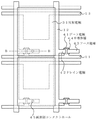
本発明の第1の実施形態について図面を参照して説明する。第1の実施形態は凹凸を有する有機層間絶縁膜上に反射電極を形成する反射型表示装置の例である。図1は、本発明の第1の実施形態の液晶表示装置に使用する薄膜トランジスタアレイ基板(TFT基板)の構成を示す概念図である。また、図2は本発明の第1の実施形態の液晶表示装置のパネル平面図、図3は図2のA−A線、C−C線及び一画素部分(後述する図4のB−B線部分の断面に対応)のパネル断面図である。
【0022】
図1、図3に示すように、TFT基板10には、透明絶縁性基板10a上に複数の走査線11と複数の信号線12がほぼ直交して配設され、その交点近傍にこれらに接続されてスイッチング素子である薄膜トランジスタ(TFT)14が設けられ、これらがマトリクス状に配置されている。また走査線と平行に複数の共通配線13が配設され、TFT14に接続される画素電極(反射電極)31との間で保持容量が形成される。液晶に電圧を印加するための反射電極31は走査線11、信号線12、TFT14とは有機層間絶縁膜32を介して分離され、この上に設けられている。有機層間絶縁膜32には凹凸が形成され、その形状を反映して反射電極31にも凹凸(反射電極の表面モホロジー凹凸とは異なる)が形成される。
【0023】
また、走査線11の端部にはアドレス信号を入力する走査線端子15が、信号線12の端部にはデータ信号を入力する信号線端子16がそれぞれ設けられている。また、共通配線13は通常TFT基板の両側で共通配線結束線17により相互に結束され、その端部に共通配線端子18が設けられ、対向基板20上の対向電極33と同電位が与えられる。ここでは、概念的に走査線端子15と信号線端子16がTFT基板10のそれぞれ一辺ずつを占めるように示しているが、本発明の液晶表示装置は小型携帯用途のため、双方がTFT基板10の一辺にまとめて設けられる。(図2参照)
一方、図2、図3に示すように、対向基板20には、透明絶縁性基板20a上に表示領域に対応してカラーフィルタ21と液晶に電圧を印加するための対向電極33が設けられ、周辺部にブラックマトリクス22が設けられている。反射電極31が遮光層も兼ねるので、表示領域にはブラックマトリクスは設けられていない。ブラックマトリクス22は液晶表示装置の見栄えをよくする(黒をより黒らしくし、見栄えを鮮明にさせる)ためのものである。
【0024】
これらのTFT基板10と対向基板20の対向面に液晶分子を配向させる配向膜34が設けられ、両基板がシール材23と面内スペーサー35とを介して所定間隔に重ね合わされ、その中に液晶36が挟持されている。液晶36を注入したシール材の空間は封孔材24で密閉されている。さらに、対向基板20のTFT基板10との対向面とは反対側の面には1/4波長板37と偏向板38が設けられ、液晶表示パネルとなる。図2には図示していないが、この後、走査線端子15と信号線端子16の部分に駆動回路であるICチップがCOG(チップオングラス)実装され、液晶表示装置が完成される。
【0025】
図3に示したように、対向基板20の裏面側から入射した入射光39は対向基板20、液晶36層を透過し、TFT基板10表面の所定の凹凸を有する反射電極31上で反射され、再び液晶36層、対向基板20を透過して、出射光40として外部に出射される。
【0026】
次に、本発明の第1の実施形態の液晶表示装置のTFT基板の構成及びその製造方法について、図4〜図8を参照して詳細に説明する。図4は本実施形態の液晶表示装置のTFT基板の一画素部分の構成を示す平面図であり、図5、図6、図7は図4のB−B線部分に対応する工程断面図である。ここでは、スイッチング素子として逆スタガード構造のTFTを用いた例を示し、図1の一番左側の最外周画素部の図を示す。また、図8は走査線端子15、信号線端子16、共通配線端子18の短辺方向(端子は平面的に見ると細長い矩形状に配置されるので、その短辺方向という意味)の工程断面図である。
【0027】
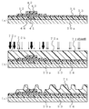
図4、図7に示すように、本実施形態の液晶表示装置のTFT基板の一画素部分は、互いに直交する走査線11及び信号線12と、これらの配線で囲まれる画素領域に各々設けられたスイッチング素子であるTFT14と、各画素領域に入射する光を反射すると共に、対向基板20との間に狭持された液晶36に電圧を印加する反射電極31と、反射電極31に所定の凹凸を形成するための第1の絶縁膜51及び第2の絶縁膜52とを含み、ゲート電極41は走査線11に、ドレイン電極42は信号線12に、ソース電極43は反射電極31に各々接続されている。なお、この反射電極31は、液晶に電圧を印加する画素電極としても機能するため、各画素毎に分離する必要があり、走査線11及び信号線12上で画素毎に分離されている。
【0028】
また、TFT側基板10は、透明絶縁性基板10a上のTFT領域にゲート電極41が形成され、その上にゲート絶縁膜53を介して半導体層44(a−Si層44a及びn +型a−Si層44b)が形成され、n +型a−Si層44b上には、ドレイン電極42及びソース電極43が形成されている。そして、各々の画素領域には、反射電極31に所定の凹凸を形成するための第1の絶縁膜51が不規則に配設され、その上には第1の絶縁膜51の段差をなだらかにする第2の絶縁膜52が形成されている。
【0029】
ここで、第1の絶縁膜51は、表示領域全面に渡って均一な反射光学特性を発揮するために、表示領域内部に不規則に形成されるが、表示領域の外側(図4の左側の領域)は、端子電極等を設ける領域であるために、第1の絶縁膜51は形成されていない。一方、第2の絶縁膜52は、コンタクトホール45部を除く表示領域内部に連続して形成されると共に、第1の絶縁膜51を完全に覆うように表示領域の外側にも多少の広がりをもって形成されている。そして、TFT14を保護するパッシベーション膜54、第1の絶縁膜51及び第2の絶縁膜52の上に反射電極31が形成され、ソース電極43上の第2の絶縁膜52、パッシベーション膜54にそれぞれ設けたコンタクトホール45、55部においてソース電極43と接続されている。
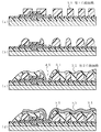
【0030】
この反射電極31表面は、第1の絶縁膜51及び第2の絶縁膜52による凹凸が反映され、反射電極31表面の凹凸傾斜角度の構成が反射光の光学特性を決定することとなる。それゆえ、凹凸の傾斜角度は所望の反射光学特性が得られるように設計される。なお、このとき凹凸は、凸ピッチ、凹ピッチ、凸高さ、凹深さのいずれかについて、異なる2種以上の値で構成されていればよい。
【0031】
また、第1の絶縁膜51の膜厚の下限は、上記反射光学特性により規定されると共に、寄生容量の観点からも制限される。すなわち、第1の絶縁膜51が薄く形成されると、入射光の反射方向を大きく変化させることができなくなると共に、反射電極31と走査線11、信号線12との間隔が狭くなるため、これらの配線との間の寄生容量が大きくなり、信号の遅延を引き起こして正しい信号の送信ができなくなったり、信号線と画素との間の電界が強まるため、付近の液晶に影響を及ぼし液晶分子の配向方向に乱れが生じたり、応答が遅くなる等、表示品位を損ねることになる。従って、第1の絶縁膜51は1〜3μm程度の膜厚で形成される。一方、第2の絶縁膜52は、第1の絶縁膜51の凹凸を適度に緩和し、表面をなだらかな曲面とするために設けるものであるため、薄すぎると上記効果を発揮することができず、また、厚すぎると第1の絶縁膜51の凹凸を相殺して平坦化してしまうことになる。従って、第2の絶縁膜52の膜厚としては、0.3〜1.5μm程度の範囲が好ましい。
【0032】
次に、上記構成のTFT基板の製造方法について説明する。図5(a)〜図7及び図8に示すように、この製造工程は、大別すると、(1)ゲート電極41の金属膜の成膜、パターンニング、(2)ゲート絶縁膜53、a−Si層44a、n +型a−Si層44bの成膜、パターンニング、(3)ドレイン電極42、ソース電極43の金属膜の成膜、パターンニング、(4)パッシベーション膜54の成膜、パターンニング、(5)端子部接続電極63の透明導電膜の成膜、パターンニング、(6)第1の絶縁膜51の成膜、パターンニング及び表面形状変換処理、(7)第2の絶縁膜52の成膜、パターンニング、(8)反射電極31の金属膜の成膜、パターンニングの全部で8工程からなる。
【0033】
まず、厚さ0.5mmの無アルカリガラスからなる透明絶縁性基板10a上に、スパッタにより厚さ100nm〜300nmのCr等の金属膜を成膜し、公知のフォトリソグラフィー技術及びエッチング技術を用いて、ゲート電極41、走査線11(図示せず)、共通配線13(図示せず)、走査線端子15、信号線端子16、共通配線端子18の端子部金属膜61を形成する。なお、配線材料としては、Crに限らず、MoやAlもしくはAl合金上にCr、Mo、チタン(Ti)等のバリアメタルを形成した積層構造の配線膜のように、抵抗が低く、薄膜形成及びフォトリソグラフィー技術によるパターンニングが容易な材料であればよい。(図5(a)、図8(a))
次に、プラズマCVDにより厚さ300nm〜500nmの窒化シリコン(SiNx)からなるゲート絶縁膜53を成膜し、引き続きプラズマCVDによりゲート絶縁膜53上に厚さ150nm〜300nmのドーピングされていないアモルファスシリコン(a−Si)と厚さ30nm〜50nmのn +型にドーピングされたアモルファスシリコン(n +型a−Si)を成膜し、フォトリソ工程を通してパターンニングし、a−Si層44aとn +型a−Si層44bからなる半導体層44を形成する。a−Si層44aはTFT14の能動層となるものであり、n +型a−Si層44bはドレイン電極42及びソース電極43とa−Si層44aとのオーミックコンタクトを確保するためのものである。(図5(b)、図8(b))
次に、スパッタにより厚さ100nm〜300nmのCr等の金属膜を成膜、フォトリソ工程を通してパターンニングし、ドレイン電極42、ソース電極43、信号線12を形成する。その後、ドレイン電極42、ソース電極43をマスクにしてドライエッチングを行い、ドレイン電極42とソース電極43の間のn +型a−Si層44bを除去する。これは、ドレイン電極42とソース電極43との間をn +型a−Si層13bを介して直接電流が流れるのを防止するためである。ここでも配線材料としては、Crに限らず、MoやAlもしくはAl合金の上下にCr、Mo、Ti等のバリアメタルを形成した積層構造の配線膜のように、抵抗が低く、薄膜形成及びフォトリソグラフィー技術によるパターンニングが容易な材料であればよい。(図5(c)、図8(b))
次に、プラズマCVDにより厚さ100nm〜300nmの窒化シリコンを成膜してパッシベーション膜54を形成し(図8(c))、ソース電極43上のパッシペーション膜54と、走査線端子15、信号線端子16、共通配線端子18の端子部金属膜61上のパッシペーション膜54及びゲート絶縁膜53とをパターニングして、それぞれコンタクトホール55および端子部コンタクトホール62を開口する。このとき、図示していないが、共通配線13の端部上のパッシベーション膜54およびゲート絶縁膜53と、信号線端子16の端子部金属膜61端部上のパッシベーション膜54及びゲート絶縁膜53と、信号線端子16側の信号線12端部上のパッシベーション膜54とを同時にパターンニングして開口する。このパッシベーション膜54は、イオン等の不純物がa−Si層44aに拡散し、TFT14が動作不良を起こすのを防ぐためのものである。(図5(d)、図8(d)) 次に、スパッタにより厚さ40nm〜100nmのITO等の透明導電膜を成膜、フォトリソ工程を通してパターンニングし、走査線端子15、信号線端子16、共通配線端子18の端子部金属膜61上に接続電極63と、共通配線13の端部上に共通配線結束線17(図示せず)と、信号線端子16の端子部金属膜61と信号線12とを接続するための接続電極(図示せず)とを形成する。このとき、表示領域には透明導電膜のパターンは形成しない。従って、ソース電極43にMoやAlもしくはAl合金の上下にMoを積層したような金属膜を用いた場合、ITOのパターニングはシュウ酸等のMoをエッチングしないエッチング液で行う必要がある。ソース電極43にCrやAlもしくはAl合金の上下にCrやTiを積層したような金属膜を用いた場合は、王水系や塩化第2鉄系のエッチング液を用いてもさしつかえない。ここで、表示領域には透明導電膜のパターンは形成しないのは、コンタクトホール55部において、後述するITO−Al間の電池作用による透明導電膜の剥がれの危険性をできるだけ回避するためである。また、走査線端子15、信号線端子16、共通配線端子18の端子部金属膜61上に透明導電膜で接続電極63を形成するのは、COG実装時の端子部での接続信頼性を確保するためである。(図5(d)、図8(e))次に、例えば、感光性ノボラック樹脂を厚さ1〜3μm塗布し、フォトリソ工程を通しアルカリ現像液でパターニングして、表示領域内部に不規則に第1の絶縁膜51を形成する。第1の絶縁膜51としては、感光性を有さない樹脂又は感光性を有する樹脂のいずれを用いることもでき、感光性を有さない樹脂を用いる場合の形成工程は、基板上への(1)第1の絶縁膜51の塗布、(2)第1の絶縁膜51のパターンニング用レジスト塗布、(3)露光、(4)現像、(5)第1の絶縁膜51のエッチング、(6)レジスト剥離の各工程処理からなる。一方、感光性を有する樹脂を用いる場合の形成工程は、基板上への(1)第1の絶縁膜51の塗布、(2)露光、(3)現像の各工程処理からなり、パターンニング用レジストの塗布、剥離の工程を省略することができる。(図6(a)、図8(e)) 次に、この第1の絶縁膜51に所定の表面形状変換処理を施して、なだらかな凸形状にする。これは、80℃〜200℃程度の温度で熱処理を行うことで、パターン形成後の第1の絶縁膜51表面をメルトさせ、滑らかな形状に変換するものである。表面形状変換処理は熱処理に限定されず、例えば、NMP(N−メチル−2−ピロリドン)のような薬品による溶融処理等を用いてもよい。表面形状変換処理後、200℃〜250℃程度の温度で再度焼成を行う。(図6(b)、図8(e))
次に、例えば、感光性ノボラック樹脂を厚さ0.3〜1.5μm塗布し、フォトリソ工程を通しアルカリ現像液でパターニングし、200℃〜250℃程度の温度で焼成して、第2の絶縁膜52を形成すると共に、ソース電極43上のパッシベーション膜54に開口されたコンタクトホール55に対応して、画素部コンタクトホール45を形成する。(図6(c)、図8(e))
ここでは、第1の絶縁膜51と第2の絶縁膜52はノボラック系の有機樹脂材料を用いた例を示した。例えば、JSR製のPC403等を用いることができる。しかし、これらの材料は、同じ種類である必要はなく、異なる種類であってもよい。また、ノボラック樹脂のみではなく、アクリル樹脂とポリイミド樹脂、シリコン窒化膜とアクリル樹脂、シリコン酸化膜とポリイミド樹脂等の無機系樹脂と有機系樹脂の組み合わせを用いても、あるいはその逆の組み合わせを用いても、所望の凹凸を形成することができる。
【0034】
また、ここではフォトリソ法を用いて第1の絶縁膜51と第2の絶縁膜52を形成する方法を述べたが、印刷法を用いてもよい。この場合は製造工程が簡略化できる。さらに、液相成長法などの湿式処理、プラズマ重合法などの乾式処理を用いて形成することもできる。即ち、本願でいう塗布系の絶縁膜(層間絶縁膜)とは出ガスを生じる絶縁膜の総称である。
【0035】
次に、スパッタにより厚さ50nm〜200nmのMo膜と厚さ100nm〜300nmのAl−Nd合金膜を順次成膜し、フォトリソ工程を通してパターンニングし、高反射率の反射電極31を形成する。このパターニングは、40℃〜60℃に加熱したリン酸、酢酸及び硝酸からなる混酸によるウェットエッチングにより行う。このとき、反射電極31は、各々の画素のソース電極43と接続され、画素電極としても機能するために、各々の画素領域の間(走査線11上、及び信号線12上)で除去されると共に、表示領域の外側も合わせて除去される。従って、走査線端子15、信号線端子16、共通配線端子18の各端子部上にはMoとAl−Nd合金膜は残っていない。ここで、Mo膜は端子部の接続電極63である透明導電膜(ITO膜)とAl−Nd合金膜とのバリアメタルであり、フォトリソ工程の現像時に現像液がしみ込んで発生するITO−Al間の電池作用による透明導電膜の剥がれを防止する役割があり、この電池作用を防止するために十分な膜厚が必要になる。(図6(d)、図8(e))
次に、反射電極31となる金属膜の成膜方法について詳細に述べる。スパッタ装置において、図6(c)、図8(e)の状態のTFT基板10をまず加熱室に搬送し、70℃〜170℃の温度に加熱して、1〜2分間程度第1及び第2の絶縁膜に含まれる水分を十分放出させる。次にTFT基板10を成膜室に搬送し、速やかにMo膜とAl−Nd合金膜の成膜を連続して行う。ここで、加熱室と成膜室は異なるチャンバーで独立に真空排気される方が望ましい。これはTFT基板10の塗布系の絶縁膜(第1及び第2の絶縁膜)からの出ガスが、Mo膜やAl−Nd合金膜の膜質や下層の金属膜との間のコンタクト抵抗に悪影響を与えないようにするためである。加熱と成膜が同じチャンバーで行われる場合は、加熱時間を2〜5分程度に長めにとり、基板加熱(保温)の最中にチャンバーを十分排気することが大切である。これにより、白濁のない高反射率のAl−Nd合金膜が得られ、同時にソース電極43と反射電極31の間のコンタクト抵抗を低く安定化できる(後述する)。
【0036】
なお、上記でMo膜成膜時の基板加熱とAl−Nd合金膜成膜時の基板加熱は必ずしも同じ温度で行う必要はなく、例えば、Mo膜成膜時を150℃、Al−Nd合金膜成膜時を120℃のように、Mo膜成膜時の基板加熱温度を高く制御してもよい。これはMo膜成膜時の基板加熱温度が低いと、Mo膜の結晶性が悪くなり、Al−Nd合金膜の膜質やAl−Nd合金/Mo膜のエッチング性に悪影響を与えるためである。
【0037】
また、Al−Nd合金膜のNd濃度は0.5wt%以上とするのが望ましい。これにより、後工程の配向膜焼成等の熱処理工程でのヒロックを抑制でき、高反射率の反射電極31が得られる。さらに、成膜時の基板温度を170℃以下にすることにより、反射電極31の表面モホロジー(微細な凹凸)を平均ピッチ1μm以下に制御でき、波長域200nm〜400nmの反射率を可視光領域の反射率の90%以上にすることできる。これにより、配向膜の種類にかかわらず、黄変のない反射電極31を得ることができる(後述する)。一方、Nd濃度は10wt%以下とするのが望ましい。これにより、高反射率のAl−Nd合金膜が得られる(後述する)。
【0038】
なお、ここでは、反射電極31の材料として、反射率が高くTFTプロセスとの整合性がよいAl−Nd合金を用いた例を示したが、これに限定されるものではなく、反射率の高い金属であれば良く、例えば、Al−Ti合金やAl−Mo合金等の他のAl合金、あるいは、さらに高反射率の銀(Ag)もしくは銀合金を用いてもよい。
【0039】
次に、上記TFT基板10の上に、印刷により厚さ50nm〜100nmの配向膜34を形成し、200℃〜230℃程度の温度で焼成し、配向処理を行う。一方、透明絶縁性基板20a上に表示領域に対応して、カラーフィルタ21とその上にITO等の透明導電膜からなる対向電極33が形成され、周辺部にブラックマトリクス22が形成された対向基板20の上に、同様に、印刷により厚さ50nm〜100nmの配向膜34を形成し、200℃〜230℃程度の温度で焼成し、配向処理を行う。ここで、配向膜は波長域300nm〜600nmの光透過率が95%以上であるものを用いるのが望ましい。これにより、黄変のない反射電極31を得ることができる(後述する)。
【0040】
これらのTFT基板10と対向基板20とを、エポキシ系樹脂接着剤からなるシール材23(図示せず)及びプラスチック粒子等からなる面内スペーサー35(図示せず)を介して、各々の膜面が対向するようにして所定間隔に重ね合わせる。その後、TFT基板10と対向基板20との間に液晶36を注入し、液晶36を注入したシール材23(図示せず)の空間(注入口)をUV硬化型アクリレート系樹脂からなる封孔材24(図示せず)で密閉する。最後に、対向基板20の膜面とは反対側の面に、1/4波長板37と偏向板38を貼って、液晶表示パネルを完成する。(図7)
この後、図示していないが、走査線端子15部、信号線端子16部、共通配線端子18部に駆動回路となるICチップをCOG実装し、液晶表示装置を完成する。以上のようにして、高反射率で黄変がなく、書き込み不良の問題のない反射型液晶表示装置が得られる。
【0041】
次に、本発明の第2の実施形態について図面を参照して説明する。第2の実施形態も凹凸を有する有機層間絶縁膜上に反射電極を形成する反射型表示装置の例である。本実施形態は、TFT基板の製造工程の簡略化を目的とするものであり、他の部分の構造、製造方法については、前述した第1の実施形態と全く同様である。
【0042】
本発明の第2の実施形態の液晶表示装置のTFT基板の構成及びその製造方法について、図4、図5、図8〜図10を参照して詳細に説明する。図4は本実施形態の液晶表示装置のTFT基板の一画素部分の構成を示す平面図であり、図5、図9〜図10は図4のB−B線部分に対応する工程断面図である。ここでは、スイッチング素子として逆スタガード構造のTFTを用いた例を示し、図1の一番左側の最外周画素部の図を示す。また、図8は走査線端子15、信号線端子16、共通配線端子18の短辺方向の工程断面図である。
【0043】
本実施形態では、図10(b)に示すように、反射電極31に所定の凹凸を形成するため、絶縁膜71が一体的に形成され、不規則にかつなだらかに配設されている。即ち、第1の実施形態における第1の絶縁膜と第2の絶縁膜の役割が、本実施形態の絶縁膜71に持たされている。
【0044】
上記構成のTFT基板の製造工程は、図5(a)〜図5(c)、図9(a)〜図10(b)及び図8に示すように、大別すると、(1)ゲート電極41の金属膜の成膜・パターンニング、(2)ゲート絶縁膜53、a−Si層44a、n +型a−Si層44bの成膜、パターンニング、(3)ドレイン電極42、ソース電極43の金属膜の成膜、パターンニング、(4)パッシベーション膜54の成膜、パターンニング、(5)端子部接続電極63の透明導電膜の成膜、パターンニング、(6)絶縁膜71の成膜、パターンニング及び表面形状変換処理、(7)反射電極31の金属膜の成膜、パターンニングの全部で7工程からなる。
【0045】
工程(1)〜(5)は、第1の実施形態と全く同様であり、透明絶縁性基板10a上にTFT14と、走査線端子15、信号線端子16、共通配線端子18を形成する。(図9(a)、図8(e))
次に、例えば、感光性ノボラック樹脂からなる絶縁膜71を厚さ2〜4.5μm塗布する。そして、この絶縁膜71を露光、現像して凹凸を形成するが、本実施形態では、フォトマスクとして露光の光を透過する透過領域と、所定の量だけ減衰して透過する半透過領域と、遮光領域とが形成されたハーフトーンマスクを用いることを特徴とする。即ち、凸部を形成する領域72aには遮光領域が対応し、凹部を形成する領域72bには半透過領域が対応し、絶縁膜71を完全に除去する領域72cには透過領域が対応するように位置合わせをして露光を行う。(図9(b))
次に、現像を行い、遮光領域では絶縁膜71はそのまま残り、半透過領域ではある程度絶縁膜71がエッチングされるために、絶縁膜71に所定の凹凸が形成される。なお、絶縁膜71を完全に除去する領域(透過領域72c)の隣には、必ずある程度の膜が残る領域(半透過領域72b)を配置するようにし、絶縁膜71によって急峻な段差が生じないようにしている。このように、露光の際に、ハーフトーンマスクを用いて、長い時間露光するか強い光を当てて、絶縁膜71を完全に感光させて現像にて絶縁膜71を完全に除去する領域、短い時間露光するか弱い光を当てて、絶縁膜71をある程度残す領域、光を当てずに膜を除去しない領域をつくることにより、第1の実施形態の第1の絶縁膜51と第2の絶縁膜52の形成工程を一つの工程で行うことができる。(図9(c))
次に、第1の実形態と同様に、表面形状変換処理を行う。これは、80℃〜200℃程度の温度で熱処理を行うことにより、パターン形成後の絶縁膜71の表面をメルトさせ、滑らかな形状に変換させる。なお、表面形状変換処理では熱処理に限定されず、例えば、薬品による溶融処理等を用いてもよい。表面形状変換処理後、200℃〜250℃程度の温度で再度焼成を行う。(図10(a))
次に、第1の実形態と同様に、スパッタにより厚さ50nm〜200nmのMo膜と厚さ100nm〜300nmのAl−Nd合金膜を順次成膜し、フォトリソ工程を通してパターンニングし、高反射率の反射電極31を形成し、TFT基板を完成させる。高反射率の反射電極31の形成方法は第1の実施形態と全く同様である。(図10(b)、図8(e))
このように、ハーフトーンマスクを用いることにより、凹凸を有する絶縁膜71を一工程で形成することができ、第1の実施形態に比べて工程の削減を図ることができる。
【0046】
なお、本実施形態では、ハーフトーンマスクを用いて凹凸を形成する方法について述べたが、ハーフトーンマスクを用いる方法の他にも、半残し領域と全残し領域用に別々のマスクを用い、露光量を変えることによって同様の凹凸を形成する方法や、露光の解像能力の限界よりも微細にパターンを配置することで、擬似的に半透過とする方法で、絶縁膜71に照射する露光量を場所によって変える方法を適用することもできる。
【0047】
次に、本発明の第3の実施形態について図面を参照して説明する。第3の実施形態は凹凸を有する有機層間絶縁膜上に反射電極を形成し、かつ透明導電膜からなる画素電極も形成する半透過型液晶表示装置の例である。本実施形態は、TFT基板の製造工程に透明導電膜からなる画素電極の形成工程が追加されるだけで、他の部分の構造、製造方法については、前述した第1の実施形態と全く同様である。
【0048】
本発明の第3の実施形態の液晶表示装置のTFT基板の構成及びその製造方法について、図11〜図15及び図8を参照して詳細に説明する。図11は本実施形態の液晶表示装置のTFT基板の一画素部分の構成を示す平面図であり、図12〜図15は図11のB−B線部分に対応する工程断面図である。ここでは、スイッチング素子として逆スタガード構造のTFTを用いた例を示し、図1の一番左側の最外周画素部の図を示す。また、図8は走査線端子15、信号線端子16、共通配線端子18の短辺方向の工程断面図である。
【0049】
本実施形態では、図11、図15に示すように、本実施形態の液晶表示装置のTFT基板の一画素部分は、互いに直交する走査線11及び信号線12と、これらの配線で囲まれる画素領域に各々設けられたスイッチング素子であるTFT14と、各画素領域に入射する光を反射、透過すると共に、対向基板20との間に狭持された液晶36に電圧を印加する反射電極31、透明導電膜からなる画素電極81と、反射電極31に所定の凹凸を形成するための第1の絶縁膜51及び第2の絶縁膜52とを含み、ゲート電極41は走査線11に、ドレイン電極42は信号線12に、ソース電極43は反射電極31に、反射電極31は透明導電膜からなる画素電極81に各々接続されている。
【0050】
ここで、反射電極31は画素電極81の周囲を囲むようにして形成され、画素電極81を構成する透明導電膜の周囲が反射電極31を構成する金属膜で被覆され、この部分で電気的接続がとられるようになっている。
【0051】
上記構成のTFT基板の製造工程は、図12(a)〜図15及び図8に示すように、大別すると、(1)ゲート電極41の金属膜の成膜・パターンニング、(2)ゲート絶縁膜53、a−Si層44a、n +型a−Si層44bの成膜、パターンニング、(3)ドレイン電極42、ソース電極43の金属膜の成膜、パターンニング及びパッシベーション膜54の成膜、(4)第1の絶縁膜51の成膜、パターンニング及び表面形状変換処理、(5)第2の絶縁膜52の成膜、パターンニング、(6)パッシベーション膜54のパターンニング、(7)画素電極81及び端子部接続電極63の透明導電膜の成膜、パターンニング、(8)反射電極31の金属膜の成膜、パターンニングの全部で8工程からなる。
【0052】
工程(1)〜(3)は、第1の実施形態のパッシベーション膜54成膜までの工程と全く同様であり、透明絶縁性基板10a上にTFT14を形成する。パッシベーション膜54の開口はこの時点では行わない。(図12(d)、図8(c))工程(4)〜(5)は、第1の実施形態の工程(6)〜(7)と全く同様である。但し、本実施形態は半透過型液晶表示装置のため、第1の絶縁膜51と第2の絶縁膜52の色つきを防止するため、現像後に全面露光を行うことが、第1の実施形態と異なる。(図13(c)、図8(c))
次に、ソース電極43上のパッシべーション膜54と、走査線端子15、信号線端子16、共通配線端子18の端子部金属膜61上のパッシベーション膜54及びゲート絶縁膜53とをパターンニングして、それぞれコンタクトホール55、端子部コンタクトホール62を開口する。このとき、図示していないが、共通配線13の端部上のパッシベーション膜54及びゲート絶縁膜53と、信号線端子16の端子部金属膜61端部上のパッシペーション膜54及びゲート絶縁膜53と、信号線端子16側の信号線12端部上のパッシペーション膜54とを、同時にパターンニングして開口する。(図14(a)、図8(d))
次に、スパッタにより厚さ40nm〜100nmのITO等の透明導電膜を成膜、フォトリソ工程を通してパターンニングし、画素電極81と、走査線端子15、信号線端子16、共通配線端子18の端子部金属膜61上に接続電極63と、共通配線13の端部上に共通配線結束線17(図示せず)と、信号線端子16の端子部金属膜61と信号線12とを接続するための接続電極(図示せず)とを形成する。このとき、透明導電膜の成膜も、第1の実施形態で述べた反射電極31となる金属膜の成膜と同様な方法で行ない、出ガスの影響を避けることが望ましい。また、ソース電極43上の画素部コンタクトホール45上には透明導電膜のパターンは形成しないのも第1の実施形態で述べた通りである。(図14(b)、図8(e))
次に、第1の実施形態と同様に、スパッタにより厚さ50nm〜200nmのMo膜と厚さ100nm〜300nmのAl−Nd合金膜を順次成膜し、フォトリソ工程を通してパターンニングし、高反射率の反射電極31を形成し、TFT基板を完成させる。高反射率の反射電極31の形成方法は第1の実形態と全く同様である。このとき、反射電極31は、各々の画素のソース電極43及び画素電極81と接続され、各々の画素領域の間(走査線11上、及び信号線12上)で除去されると共に、表示領域の外側も合わせて除去される。従って、走査線端子15、信号線端子16、共通配線端子18の各端子部上にはMoとAl−Nd合金膜は残っていない。この事情も、第1の実施形態と全く同様である。また、画素電極81を構成する透明導電膜(ITO膜)の周囲を反射電極31を構成する金属膜(Al−Nd合金/Mo膜)で被覆するようにしているので、フォトリソ工程の現像時に現像液が金属膜を通して透明導電膜の端部からしみ込む危険性がなく(透明導電膜の端部上はフォトレジストが現像されず、金属膜が現像液にさらされることがないため)、ITO−Al間の電池作用による透明導電膜の剥がれを防止することができ、液晶表示装置の点欠陥不良を大幅に低減できる。(図14(c)、図8(e))
以降、第1の実施形態と全く同様にして、液晶表示パネルを製造し(図15)、液晶表示装置を完成する。以上のようにして、高反射率で黄変がなく、書き込み不良の問題のない半透過型液晶表示装置が得られる。
【0053】
次に、本発明の第4の実施形態について図面を参照して説明する。第4の実施形態は、第1から第3までの実施形態のように、出射光の散乱を凹凸を有する反射電極で行うのではなく、対向基板20側のカラーフィルタ21上につけた散乱膜91で行う反射型液晶表示装置の例である。本実施形態では、TFT基板10に凹凸を有する絶縁膜を形成する工程がない。即ち、反射電極31は、パッシベーション膜54上に直接形成される。
【0054】
本発明の第4の実施形態の液晶表示装置の構成及びその製造方法について、図16を参照して簡単に説明する。図16は本実施形態の液晶表示装置のパネル断面図であり、図2のA−A線、C−C線及び一画素部分の断面図である(B−B線部分は図4に示される断面に対応している)。
【0055】
上記構成の液晶表示装置のTFT基板の製造工程は、大別すると、(1)ゲート電極41の金属膜の成膜・パターンニング、(2)ゲート絶縁膜53、a−Si層44a、n +型a−Si層44bの成膜、パターンニング、(3)ドレイン電極42、ソース電極43の金属膜の成膜、パターンニング、(4)パッシベーション膜54の成膜、パターンニング、(5)端子部接続電極63の透明導電膜の成膜、パターンニング、(6)反射電極31の金属膜の成膜、パターンニングの全部で6工程からなる。これは、第1の実施形態から工程(6)〜工程(7)を削除したものであるので、説明は省略する。
【0056】
但し、反射電極31が、塗布系の絶縁膜でなく、プラズマCVDにより形成された窒化シリコンからなるパッシベーション膜54上に形成されるため、反射電極となる金属膜の成膜方法が第1の実施形態と少し異なる。つまり、本実施形態では、スパッタ装置において、図5(d)、図8(e)の状態のTFT基板10をまず加熱室に搬送し、室温のまま、または170℃以下の温度に加熱した後、TFT基板10を成膜室に搬送し、速やかにMo膜とAl−Nd合金膜の成膜を連続して行う。ここで、加熱室と成膜室は同じチャンバーであっても、異なるチャンバーであってもよい。これは第1の実施形態と異なり、TFT基板10には塗布系の絶縁膜が存在せず、出ガスの影響がほとんどないためである。これにより、白濁のない高反射率のAl−Nd合金膜が得られる(後述する)。本実施形態では、パッシベーション膜54の膜厚を300nm〜800nm程度に厚くするのが望ましい。なお、パッシベーション膜54上を塗布系の絶縁膜で平坦化する場合は、第1の実施形態で工程(6)(第1の絶縁膜51による凹凸形成工程)が削除されるだけであり、反射電極となる金属膜の成膜方法は第1の実施形態と同じになるので、出ガスの影響をほとんどなくすという目的を有する本実施形態にはそぐわない。
【0057】
また、Al−Nd合金膜のNd濃度については、第1の実施形態と全く同様に、0.5wt%以上10wt%以下とするのが望ましい。さらに、成膜時の基板温度を170℃以下にすることにより、反射電極の表面モホロジー(微細な凹凸)を平均ピッチ1μm以下に制御でき、波長域200nm〜400nmの反射率を波長400nmでの反射率の90%以上にすることできる。これにより、後工程の配向膜焼成等の熱処理工程でのヒロックを抑制でき、高反射率の反射電極31が得られると同時に、配向膜の種類にかかわらず、黄変のない反射電極31を得ることができる(後述する)。
【0058】
以降、第1の実施形態と同様にして、液晶表示パネルを製造し、液晶表示装置を完成するが、第1の実施形態と異なるのは、対向基板20のカラーフィルタ21上に散乱膜91を設けていることである。この散乱膜91は、例えば、ノボラック系樹脂の中にプラスチック粒子等からなるビーズを混入したものから構成されている。プラスチック粒子の径や配合割合を最適化することにより、凹凸を形成した反射電極と同様な散乱効果が得られる。以上のようにして、高反射率で黄変がなく、書き込み不良の問題のない反射型液晶表示装置が得られる。
【0059】
なお、以上の実施形態では、スイッチング素子として逆スタガードチャネルエッチ型のTFTを用いた例を述べたが、チャネル保護型のTFTや順スタガード型のTFTを用いてもよい。また、これらスタガード型のTFTのみならずコプレナー型のTFTを用いてもよく、さらに、ポリシリコン(p−Si)TFTを用いてもよい。また、スイッチング素子として、TFTでなく、MIMダイオードを用いてもよい。また、スイッチング素子を有する基板と対向基板は、ガラス基板でなく、これ以外の基板、例えばプラスチック基板、セラミックス基板、半導体基板(半透過型液晶表示装置の場合は除く)等を用いてもよい。
【0060】
さらに、本発明は、アクティブマトリックス型液晶表示装置のみならず、STN液晶表示装置等にも適用できる。また、第4の実施形態の反射電極となる金属膜の成膜方法は、下地に塗布系の絶縁膜を用いない、例えば、反射電極の凹凸を粗面化したガラス基板で形成するような、反射型もしくは半透過型液晶表示装置全般に広く応用できることは言うまでもない。
【0061】
次に、本発明の数値限定の根拠について、図17〜図23を参照して以下に説明する。
【0062】
図17は、Al−Nd合金成膜時の基板温度とAl−Nd合金膜の微細な表面凹凸の平均ピッチとの関係を示すグラフの一例である。ここで、Al−Nd合金の組成はNd4.5wt%のものを用い、これをガラス基板上にスパッタにより基板温度を変えて成膜し、サンプルとした。表面凹凸は5万倍の真上からのSEM写真を撮り、定規で計測して求めた。サンプルの斜め方向からのSEM写真から、Alの表面モホロジーは基板温度が下がるにつれて微細になり、凹凸の大きさ、深さ共小さくなることを確認した。基板温度が200℃のときは、凹凸の平均ピッチは1.5μm程度だが、150℃で0.9μm程度、100℃以下で0.5μm以下となることがわかった。一方、凹凸の深さは、正確ではないが、基板温度が200℃のとき0.5μm程度、150℃のとき0.3μm程度、100℃以下で0.1μm〜0.2μm程度になっている。
【0063】
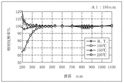
図18は、図17の成膜により得られたAl−Nd合金膜の反射率を示すグラフの一例である。ここで、反射率は測定装置に付属しているAl蒸着膜の反射率を100%として規格化している。成膜時の基板温度が120℃のときは、短波長側になるにつれて、反射率が徐々に上がっていることがわかる。一方、成膜時の基板温度が200℃のときは、400nm程度までは、同じ傾向を示すが、200nm〜400nmの波長域で急激に反射率が低下することがわかった。
【0064】
図19、図20は、Al−Nd合金膜の膜厚がそれぞれ150nm、300nmのときの、成膜時の基板温度による反射率を示すグラフの一例である。この反射率は図18で成膜時の基板温度が120℃のときのサンプルの反射率を100%として規格化した相対的な反射率である。グラフ中でRTは室温で成膜したデータである。成膜時の基板温度が150℃以上では、200nm〜400nmの波長域で反射率が低下する傾向が見られ、特に、200℃のときは急激に低下することがわかる。また、Al膜厚が厚いほど、この傾向が大きいことがわかる。
【0065】
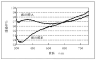
図21は配向膜の透過率を示すグラフの一例である。ここでは、日産化学製の配向膜とJSR製の一般的な配向膜を用いた。配向膜によっては、600nmより短波長側の透過率が低下するものがあることがわかった。成分であるポリイミド等に色がつきやすい材料を用いた場合、このような透過率特性になると推定される。
【0066】
図22はAl−Nd合金のNd濃度と熱処理によるヒロック及び反射率との関係を示す表である。ここで、ヒロックは、配向膜焼成と同等の230℃、1時間の熱処理行い、光学顕微鏡により観察した。Nd濃度が0.1wt%のときはヒロックが発生した(×印)が、0.5wt%以上では発生しなかった(○印)。また、反射率は、Nd濃度が0.1wt%〜5wt%では、室温で成膜した純Alと同等の反射率を維持できたが、10wt%では波長400nmで約6〜8%低下し、さらに、20wt%では、波長400nmで10%以上低下した。
【0067】
図23はAl−Nd合金(Nd濃度4.5wt%)の成膜時の基板温度と製造した液晶表示装置の色見、反射率及び下層金属膜と反射電極となる金属膜とのコンタクト抵抗との関係を示す表である。色見については、Al−Nd合金の成膜時の基板温度が200℃のときで、かつ、配向膜を図21に示した配向膜Bのような透過率特性を持つものを用いたときのみ、黄変が観察された(×印)。また、反射率については、基板温度が170℃、200℃では、波長400nmで約1〜5%低下した(△印)(図19、図20参照)。基板温度が20℃(室温)では、ガラス上では全く問題ないが、有機絶縁膜上では、出ガスの影響で白濁を生じ、波長400nmで5%程度低下した(△印)。また、コンタクト抵抗については、基板温度が70℃以上の場合は問題なかったが、基板温度が20℃(室温)では、出ガスの影響でコンタクト抵抗の増大が確認された(×印)。
【0068】
以上の実験結果を総合すると、液晶表示装置の反射電極を構成するAl−Nd合金膜に関し、下地がプラズマCVD法で形成された窒化シリコンのような絶縁膜の場合は、その成膜温度は170℃以下であることが望ましい。一方、下地が樹脂のような塗布系の絶縁膜の場合は、70℃以上170℃以下であることが望ましい。これにより、配向膜に図21の配向膜Bのような透過率特性のものを用いた場合でも、液晶表示装置の色見の黄変を防止し、高反射率にすることができる。同時に、下層金属膜と反射電極となる金属膜とのコンタクト不良を防止することができる。このとき、図17から、反射電極を構成するAl−Nd合金膜の表面モホロジーは、その微細な凹凸の平均ピッチが1μm以下であることが望ましく、さらに望ましくは、0.6μm以下であればよい。即ち、このような表面モホロジーに制御する必要がある。また、図19、図20から、反射電極を構成するAl−Nd合金膜の反射率は、波長域200nm〜400nmの反射率が波長400nmでの反射率の95%以上であることが望ましい。すなわち、このような反射率特性を有する膜質に制御する必要がある。
【0069】
一方、反射電極を構成するAl−Nd合金膜のNd組成は0.5wt%以上10wt%以下であることが望ましく、さらに望ましくは、0.5wt%以上5wt%以下であればよい。これにより、後工程での熱処理による反射電極へのヒロックの発生を防止でき(従って、配向処理時のラビングロールの汚染等を防止でき)、同時に、高反射率の液晶表示装置にすることができる。
【0070】
また、液晶表示装置の反射電極上に形成される配向膜は、波長域300nm〜600nmの光透過率が95%以上であることが望ましい。これにより、液晶表示装置の色見の黄変を防止することができる。
【0071】
反射電極の表面モホロジーと配向膜との組合せで、反射型もしくは半透過型液晶表示装置の色見の黄変が発生するのは、いまだ明確ではないが、次のようなメカニズムが推定される。即ち、反射電極表面の凹凸が大きいと、この中に配向膜が入りこみ、配向膜を通過する光路が実効的に長くなり、その分、図21の配向膜Bのような吸収を受けやすくなるためと考えられる。特に、反射型液晶表示装置では、配向膜を光が計4回通過するため、透過型液晶表示装置よりも配向膜による光吸収が多くなる。紫外光領域での光吸収が増えた結果、液晶表示装置の色見が黄変すると考えられる。
【0072】
ここで述べた事情は、反射電極がAl−Nd合金や他のAl合金の場合のみならず、他の反射電極材料、例えば、Alよりも反射率の高い銀、銀合金の場合も全く同じように当てはまると考えられる。
【0073】
【発明の効果】
以上説明したように、本発明によれば、高反射率で色見に黄変がなく、ソース電極と反射電極間のコンタクト抵抗に起因する書き込み不良のない反射型もしくは半透過型液晶表示装置を高歩留で提供することができる。
【図面の簡単な説明】
【図1】本発明の第1の実施形態の液晶表示装置に使用する薄膜トランジスタアレイ基板(TFT基板)の構成を示す概念図である。(第2、第3及び第4の実施形態と共通)
【図2】本発明の第1の実施形態の液晶表示装置のパネル平面図である。(第2、第3及び第4の実施形態と共通)
【図3】図2のA−A線、C−C線及び一画素部分(図4のB−B線部分の断面に対応)のパネル断面図である。
【図4】本発明の第1の実施形態の液晶表示装置のTFT基板の一画素部分の構成を示す平面図である。(第2の実施形態と共通)
【図5】図4のB−B線部分に対応する工程断面図である。(第2の実施形態と共通)
【図6】図5に続く製造工程を示す工程断面図である。(第2の実施形態と共通)
【図7】図6に続く製造工程を示す工程断面図であり、パネル断面図である。
【図8】本発明の第1の実施形態の液晶表示装置の走査線端子15、信号線端子16、共通配線端子18の短辺方向の工程断面図である。(第2及び第3の実施形態と共通)
【図9】本発明の第2の実施形態の液晶表示装置のTFT基板の製造工程を示す工程断面図であり、図4のB−B線部分に対応し、図5の工程(c)に続く工程断面図である。
【図10】図9に続く製造工程を示す工程断面図である。
【図11】本発明の第3の実施形態の液晶表示装置のTFT基板の一画素部分の構成を示す平面図である。
【図12】図11のB−B線部分に対応する工程断面図である。
【図13】図12に続く製造工程を示す工程断面図である。
【図14】図13に続く製造工程を示す工程断面図である。
【図15】図14に続く製造工程を示す工程断面図であり、パネル断面図である。
【図16】本発明の第4の実施形態の液晶表示装置のパネル断面図であり、図2のA−A線、C−C線及び一画素部分(図4のB−B線部分の断面に対応)の断面図である。
【図17】Al−Nd合金成膜時の基板温度とAl−Nd合金膜の表面凹凸の平均ピッチとの関係を示すグラフの一例である。
【図18】図17の成膜により得られたAl−Nd合金膜の反射率を示すグラフの一例である。
【図19】Al−Nd合金膜の膜厚が150nmのときの、成膜時の基板温度による反射率を示すグラフの一例である。
【図20】Al−Nd合金膜の膜厚が300nmのときの、成膜時の基板温度による反射率を示すグラフの一例である。
【図21】配向膜の透過率を示すグラフの一例である。
【図22】Al−Nd合金のNd濃度と熱処理によるヒロック及び反射率との関係を示す表である。
【図23】Al−Nd合金(Nd濃度4.5wt%)の成膜時の基板温度と製造した液晶表示装置の色見、反射率及び下層金属膜と反射電極となる金属膜とのコンタクト抵抗との関係を示す表である。
【図24】従来の一般的な反射型液晶表示装置の断面図である。
【符号の説明】
10 TFT基板
11 走査線
12 信号線
13 共通配線
14 TFT
15 走査線端子
16 信号線端子
17 共通配線結束線
18 共通配線端子
20 対向基板
21 カラーフィルタ
22 ブラックマトリクス
23 シール材
24 封孔材
31 反射電極
32 有機層間絶縁膜
33 対向電極
34 配向膜
35 面内スペーサー
36 液晶
37 1/4波長板
38 偏向板
41 ゲート電極
42 ドレイン電極
43 ソース電極
44 半導体層
45 画素部コンタクトホール
51 第1の絶縁膜
52 第2の絶縁膜
53 ゲート絶縁膜
54 パッシベーション膜
55 コンタクトホール
61 端子部金属膜
62 端子部コンタクトホール
63 接続電極
71 絶縁膜
81 画素電極
91 散乱膜[0001]
BACKGROUND OF THE INVENTION
The present invention relates to a liquid crystal display device and a method for manufacturing the same, and more particularly to a reflective liquid crystal display device having a reflective electrode or a reflective / transmissive (hereinafter referred to as semi-transmissive) liquid crystal display device and a method for manufacturing the same.
[0002]
[Prior art]
In recent years, small liquid crystal display devices for portable and PDA applications have been widely used. Reflective or transflective liquid crystal display devices are used as liquid crystal display devices used for these because of demands for light weight, thickness reduction, and low power consumption.
[0003]
FIG. 24 is a sectional view of a general reflective liquid crystal display device disclosed in Japanese Patent Application Laid-Open No. 2000-258787.
[0004]
In this reflective liquid crystal display device, a thin film transistor (TFT) as a switching element is formed on an insulating substrate (TFT substrate) 110 made of quartz glass, non-alkali glass or the like. First, a gate electrode 111 made of a refractory metal such as chromium (Cr) or molybdenum (Mo), a gate insulating film 112, and an
[0005]
Next, the entire surface of the gate insulating film 112, the
[0006]
Further, the
[0007]
Here, the reflective electrode 119 is made of an alloy of Al and neodymium (Nd). By setting the Nd concentration to 1 wt% or more, hillocks are not generated, the surface becomes flat, and even if the film is formed at a substrate temperature of about 200 ° C., it is the same as pure Al formed at room temperature (non-heated) Describes that a reflective electrode having a high reflectance can be obtained.
[0008]
On the other hand, in Japanese Patent Laid-Open No. 5-80327, as a method of manufacturing a diffuse reflection plate for liquid crystal display, when a reflective film is formed on an organic film, the heating is performed at 100 ° C. to 250 ° C. And wrinkles in the organic film due to the difference in thermal expansion coefficient, and further grain growth of the Al film or platinum (Pt) film constituting the reflective film at the time of film formation, forming fine irregularities in the reflective film, It is stated that the scattering and reflection characteristics are improved.
[0009]
Japanese Patent Laid-Open No. 2000-111906 discloses a method for manufacturing an electro-optical device in which a reflective layer having irregularities is formed, by forming irregularities under the reflective layer and forming a reflective layer on the irregularities. A film is formed under the conditions of 80 to 250 angstroms / min and a film forming temperature of 100 ° C. to 300 ° C. Further, after the metal film is formed, heat treatment is performed, and the metal film surface has an average pitch of 1 to 2 μm and a depth of 0.2 μm It is stated that fine irregularities are formed to improve the scattering reflection characteristics.
[0010]
[Problems to be solved by the invention]
However, even if an Al—Nd alloy as described in Japanese Patent Laid-Open No. 2000-258787 is used for the metal film that becomes the reflective electrode of the reflective liquid crystal display device or the transflective liquid crystal display device, the experiment of the present inventor is performed. Thus, it has been found that when the film is formed at a relatively high temperature of about 200 ° C., there is a problem that the color of the liquid crystal display device turns yellow (the appearance becomes yellowish) depending on the alignment film material (described later). ).
[0011]
On the other hand, when the metal film serving as the reflective electrode is formed without heating or at a low temperature of less than 70 ° C., a reflective liquid crystal display device in which the switching element and the reflective electrode are connected via a coating type interlayer insulating film or a half In the case of a transmissive liquid crystal display device, there is a problem that contact resistance between a metal film serving as a reflective electrode and a lower layer metal film serving as an electrode of a switching element is increased, and writing to the pixel electrode is deteriorated. In addition, when the metal film to be the reflective electrode is formed without heating, the metal film is altered by the outgas from the organic interlayer insulating film due to the temperature rise of the substrate due to the condensation heat at the time of film formation, and the reflectivity is increased. There is a problem of lowering. This phenomenon is particularly noticeable when Al or an alloy mainly composed of Al is used for the metal film to be the reflective electrode. In this case, there is a problem that Al becomes cloudy (white cloudy and reflectance decreases).
[0012]
An object of the present invention is to provide a reflective liquid crystal display device or a transflective liquid crystal display device that can prevent yellowing of the color of the liquid crystal display device, can obtain a high reflectance, and has no writing defects. It is to be.
[0013]
[Means for Solving the Problems]
The liquid crystal display device according to the present invention includes a bus wiring on a substrate, a switching element connected to the bus wiring, and a reflective electrode connected to the switching element. Depending on crystal structure The surface irregularities are characterized by an average pitch of 1 μm or less.
[0014]
The liquid crystal display device of the present invention is characterized in that, in the liquid crystal display device, the reflectance of the reflective electrode in the wavelength range of 200 nm to 400 nm is 90% or more of the reflectance at a wavelength of 400 nm.
[0015]
In the liquid crystal display device of the present invention, the reflective electrode is made of an alloy of Al and Nd, and the concentration of Nd is 0.5 wt% or more and 10 wt% or less.
[0016]
The liquid crystal display device according to the present invention is characterized in that, in the liquid crystal display device, the light transmittance in the wavelength region of 300 nm to 600 nm of the alignment film formed on the reflective electrode is 95% or more.
[0017]
Furthermore, the manufacturing method of the liquid crystal display device of the present invention is a method of manufacturing a liquid crystal display device having a bus wiring on a substrate, a switching element connected to the bus wiring, and a reflective electrode connected to the switching element. The substrate temperature during the formation of the reflective electrode is 170 ° C. or lower.
[0018]
The method for manufacturing a liquid crystal display device according to the present invention is the method for manufacturing a liquid crystal display device, wherein the reflective electrode is formed on a coating type interlayer insulating film, and the substrate temperature during the film formation is 70 ° C. or more and 170 ° C. It is characterized by the following.
[0019]
The method for manufacturing a liquid crystal display device according to the present invention is characterized in that the substrate is heated at least before the film formation when the reflective electrode is formed.
[0020]
As described above, by using an alloy of Al and Nd for a reflective electrode of a reflective liquid crystal display device or a transflective liquid crystal display device and performing film formation at a temperature of 170 ° C. or less, the average pitch of fine surface irregularities can be reduced. It is possible to form a reflective electrode having a fine morphology with less unevenness of 1 μm or less, preferably 0.6 μm or less, thereby reducing light absorption in the ultraviolet light region of a wavelength of 200 nm to 400 nm. Changes can be prevented. In addition, the morphology mentioned here refers to the surface form by the crystal structure of the metal film constituting the reflective electrode, and is a fine unevenness on the surface of the reflective electrode. Therefore, the reflective electrode is different from the unevenness reflected by the unevenness of the base film. (same as below)
At the same time, particularly in the case of a reflective liquid crystal display device or a transflective liquid crystal display device in which a reflective electrode is formed on a coating type interlayer insulating film, an alloy of Al and Nd is used for the reflective electrode, and the substrate is preliminarily set at 70 ° C. By forming the film by heating to a temperature of 0 ° C., the influence of the outgas from the interlayer insulating film of the coating system is eliminated, the cloudiness of the reflective electrode is prevented, the reflectance is high, and the metal film that becomes the reflective electrode It is possible to prevent an increase in contact resistance with the lower layer metal film serving as the electrode of the switching element.
[0021]
DETAILED DESCRIPTION OF THE INVENTION
A first embodiment of the present invention will be described with reference to the drawings. The first embodiment is an example of a reflective display device in which a reflective electrode is formed on an organic interlayer insulating film having irregularities. FIG. 1 is a conceptual diagram showing a configuration of a thin film transistor array substrate (TFT substrate) used in the liquid crystal display device according to the first embodiment of the present invention. 2 is a panel plan view of the liquid crystal display device according to the first embodiment of the present invention, and FIG. 3 is a line AA, CC line and one pixel portion of FIG. 2 (BB in FIG. 4 described later). It is a cross-sectional view of a panel corresponding to the cross section of the line portion).
[0022]
As shown in FIGS. 1 and 3, the
[0023]
A
On the other hand, as shown in FIGS. 2 and 3, the
[0024]
An
[0025]
As shown in FIG. 3, incident light 39 incident from the back side of the
[0026]
Next, the configuration of the TFT substrate of the liquid crystal display device according to the first embodiment of the present invention and the manufacturing method thereof will be described in detail with reference to FIGS. FIG. 4 is a plan view showing the configuration of one pixel portion of the TFT substrate of the liquid crystal display device of this embodiment, and FIGS. 5, 6, and 7 are process sectional views corresponding to the BB line portion of FIG. is there. Here, an example in which a reverse staggered TFT is used as a switching element is shown, and a diagram of the leftmost outermost pixel portion in FIG. 1 is shown. FIG. 8 is a process cross section in the short side direction of the
[0027]
As shown in FIGS. 4 and 7, one pixel portion of the TFT substrate of the liquid crystal display device according to the present embodiment is provided in each of a scanning line 11 and a
[0028]
The
[0029]
Here, the first insulating
[0030]
The surface of the
[0031]
Further, the lower limit of the film thickness of the first insulating
[0032]
Next, a manufacturing method of the TFT substrate having the above configuration will be described. As shown in FIG. 5A to FIG. 7 and FIG. 8, this manufacturing process is roughly divided into (1) film formation and patterning of the gate electrode 41, and (2)
[0033]
First, on a transparent
Next, a
Next, a metal film such as Cr having a thickness of 100 nm to 300 nm is formed by sputtering and patterned through a photolithography process to form the
Next, a silicon nitride film having a thickness of 100 nm to 300 nm is formed by plasma CVD to form a passivation film 54 (FIG. 8C), the
Next, for example, a photosensitive novolac resin is applied in a thickness of 0.3 to 1.5 μm, patterned with an alkali developer through a photolithography process, and baked at a temperature of about 200 ° C. to 250 °
Here, an example in which the first insulating
[0034]
Although the method of forming the first insulating
[0035]
Next, a Mo film having a thickness of 50 nm to 200 nm and an Al—Nd alloy film having a thickness of 100 nm to 300 nm are sequentially formed by sputtering and patterned through a photolithography process to form a
Next, a method for forming a metal film to be the
[0036]
Note that the substrate heating at the time of forming the Mo film and the substrate heating at the time of forming the Al—Nd alloy film do not necessarily have to be performed at the same temperature. The substrate heating temperature at the time of forming the Mo film may be controlled to be high, such as 120 ° C. during the film formation. This is because if the substrate heating temperature during the formation of the Mo film is low, the crystallinity of the Mo film is deteriorated, and the film quality of the Al—Nd alloy film and the etching property of the Al—Nd alloy / Mo film are adversely affected.
[0037]
The Nd concentration of the Al—Nd alloy film is desirably 0.5 wt% or more. Thereby, the hillock in heat processing processes, such as alignment film baking of a post process, can be suppressed, and the
[0038]
Here, an example in which an Al—Nd alloy having a high reflectivity and a good consistency with the TFT process is used as the material of the
[0039]
Next, an
[0040]
The film surfaces of the
Thereafter, although not shown, an IC chip serving as a drive circuit is COG mounted on the
[0041]
Next, a second embodiment of the present invention will be described with reference to the drawings. The second embodiment is also an example of a reflective display device in which a reflective electrode is formed on an organic interlayer insulating film having irregularities. This embodiment is intended to simplify the manufacturing process of the TFT substrate, and the structure of other parts and the manufacturing method are exactly the same as those of the first embodiment described above.
[0042]
The configuration of the TFT substrate of the liquid crystal display device according to the second embodiment of the present invention and the manufacturing method thereof will be described in detail with reference to FIGS. 4, 5, and 8 to 10. FIG. 4 is a plan view showing the configuration of one pixel portion of the TFT substrate of the liquid crystal display device of this embodiment, and FIGS. 5 and 9 to 10 are process cross-sectional views corresponding to the BB line portion of FIG. is there. Here, an example in which a reverse staggered TFT is used as a switching element is shown, and a diagram of the leftmost outermost pixel portion in FIG. 1 is shown. FIG. 8 is a process sectional view in the short side direction of the
[0043]
In the present embodiment, as shown in FIG. 10B, in order to form predetermined unevenness on the
[0044]
As shown in FIGS. 5A to 5C, FIGS. 9A to 10B, and FIG. 8, the manufacturing process of the TFT substrate having the above structure is roughly divided into (1) gate electrode. 41 metal film formation and patterning, (2)
[0045]
Steps (1) to (5) are exactly the same as those of the first embodiment, and the
Next, for example, an insulating film 71 made of a photosensitive novolac resin is applied to a thickness of 2 to 4.5 μm. Then, the insulating film 71 is exposed and developed to form irregularities, but in this embodiment, as a photomask, a transmissive region that transmits exposure light, a semi-transmissive region that attenuates and transmits a predetermined amount, A halftone mask in which a light shielding region is formed is used. In other words, the light shielding region corresponds to the region 72a forming the convex portion, the semi-transmissive region corresponds to the region 72b forming the concave portion, and the transmissive region corresponds to the region 72c from which the insulating film 71 is completely removed. Align and align the exposure. (Fig. 9 (b))
Next, development is performed, and the insulating film 71 remains as it is in the light shielding region, and the insulating film 71 is etched to some extent in the semi-transmissive region, so that predetermined unevenness is formed in the insulating film 71. It should be noted that a region where a certain amount of film remains (semi-transmissive region 72b) is always arranged next to a region where the insulating film 71 is completely removed (transmission region 72c), and no steep step is generated by the insulating film 71. I am doing so. As described above, in the exposure, the halftone mask is used to expose the insulating film 71 for a long time or to expose the insulating film 71 completely by applying strong light, and the region where the insulating film 71 is completely removed by development is short. The first insulating
Next, similarly to the first embodiment, surface shape conversion processing is performed. In this process, the surface of the insulating film 71 after pattern formation is melted and converted into a smooth shape by performing heat treatment at a temperature of about 80 ° C. to 200 ° C. Note that the surface shape conversion process is not limited to heat treatment, and for example, a melting process using chemicals or the like may be used. After the surface shape conversion treatment, firing is performed again at a temperature of about 200 ° C to 250 ° C. (Fig. 10 (a))
Next, as in the first embodiment, a Mo film having a thickness of 50 nm to 200 nm and an Al—Nd alloy film having a thickness of 100 nm to 300 nm are sequentially formed by sputtering, patterned through a photolithography process, and a high reflectance. The
Thus, by using the halftone mask, the insulating film 71 having projections and depressions can be formed in one step, and the number of steps can be reduced as compared with the first embodiment.
[0046]
In the present embodiment, the method of forming irregularities using a halftone mask has been described. However, in addition to the method using a halftone mask, exposure is performed using separate masks for the half-remaining region and the entire remaining region. Exposure amount to irradiate the insulating film 71 by a method of forming the same unevenness by changing the amount, or a method of making the pattern semi-transparent by arranging a pattern finer than the limit of the resolution of exposure. It is also possible to apply a method of changing the position depending on the location.
[0047]
Next, a third embodiment of the present invention will be described with reference to the drawings. The third embodiment is an example of a transflective liquid crystal display device in which a reflective electrode is formed on an organic interlayer insulating film having irregularities and a pixel electrode made of a transparent conductive film is also formed. In this embodiment, a pixel electrode forming process made of a transparent conductive film is added to the TFT substrate manufacturing process, and the structure and manufacturing method of the other parts are exactly the same as those of the first embodiment described above. is there.
[0048]
The configuration of the TFT substrate of the liquid crystal display device according to the third embodiment of the present invention and the manufacturing method thereof will be described in detail with reference to FIGS. FIG. 11 is a plan view showing a configuration of one pixel portion of the TFT substrate of the liquid crystal display device of the present embodiment, and FIGS. 12 to 15 are process cross-sectional views corresponding to the BB line portion of FIG. Here, an example in which a reverse staggered TFT is used as a switching element is shown, and a diagram of the leftmost outermost pixel portion in FIG. 1 is shown. FIG. 8 is a process sectional view in the short side direction of the
[0049]
In the present embodiment, as shown in FIGS. 11 and 15, one pixel portion of the TFT substrate of the liquid crystal display device of the present embodiment includes a scanning line 11 and a
[0050]
Here, the
[0051]
As shown in FIGS. 12A to 15 and 8, the manufacturing process of the TFT substrate having the above configuration is roughly divided into (1) film formation / patterning of the metal film of the gate electrode 41, and (2) gate. Insulating
[0052]
Steps (1) to (3) are exactly the same as the steps up to the formation of the
Next, the
Next, a transparent conductive film such as ITO having a thickness of 40 nm to 100 nm is formed by sputtering and patterned through a photolithography process, and the pixel electrode 81, the
Next, as in the first embodiment, a Mo film having a thickness of 50 nm to 200 nm and an Al—Nd alloy film having a thickness of 100 nm to 300 nm are sequentially formed by sputtering, and patterned through a photolithography process to obtain a high reflectance. The
Thereafter, a liquid crystal display panel is manufactured in the same manner as in the first embodiment (FIG. 15), and the liquid crystal display device is completed. As described above, a transflective liquid crystal display device with high reflectivity, no yellowing, and no problem of writing failure can be obtained.
[0053]
Next, a fourth embodiment of the present invention will be described with reference to the drawings. In the fourth embodiment, unlike the first to third embodiments, the scattering of the emitted light is not performed by the reflective electrode having unevenness, but the scattering film 91 provided on the
[0054]
A configuration of a liquid crystal display device according to a fourth embodiment of the present invention and a manufacturing method thereof will be briefly described with reference to FIG. 16 is a panel cross-sectional view of the liquid crystal display device of the present embodiment, and is a cross-sectional view of the AA line, the CC line, and one pixel portion of FIG. 2 (the BB line portion is shown in FIG. 4). Corresponds to the cross section).
[0055]
The manufacturing process of the TFT substrate of the liquid crystal display device having the above configuration can be broadly divided into (1) film formation / patterning of the metal film of the gate electrode 41, and (2)
[0056]
However, since the
[0057]
The Nd concentration of the Al—Nd alloy film is desirably 0.5 wt% or more and 10 wt% or less, just as in the first embodiment. Furthermore, by setting the substrate temperature during film formation to 170 ° C. or less, the surface morphology (fine irregularities) of the reflective electrodes can be controlled to an average pitch of 1 μm or less, and the reflectance in the wavelength range of 200 nm to 400 nm is reflected at the wavelength of 400 nm. It can be 90% or more of the rate. Thereby, hillocks in a heat treatment step such as alignment film baking in the subsequent step can be suppressed, and a
[0058]
Thereafter, in the same manner as in the first embodiment, a liquid crystal display panel is manufactured and a liquid crystal display device is completed. The difference from the first embodiment is that a scattering film 91 is formed on the
[0059]
In the above embodiment, an example of using an inverted staggered channel etch type TFT as a switching element has been described. However, a channel protection type TFT or a forward staggered type TFT may be used. In addition to these staggered TFTs, coplanar TFTs may be used, and polysilicon (p-Si) TFTs may also be used. Further, an MIM diode may be used as the switching element instead of the TFT. In addition, the substrate having the switching element and the counter substrate may be other than the glass substrate, for example, a plastic substrate, a ceramic substrate, a semiconductor substrate (except for a transflective liquid crystal display device), or the like.
[0060]
Furthermore, the present invention can be applied not only to an active matrix liquid crystal display device but also to an STN liquid crystal display device. In addition, the method for forming a metal film to be a reflective electrode according to the fourth embodiment does not use a coating-type insulating film as a base, for example, the reflective electrode is formed with a roughened glass substrate. Needless to say, the present invention can be widely applied to all reflective or transflective liquid crystal display devices.
[0061]
Next, the grounds for limiting the numerical values of the present invention will be described below with reference to FIGS.
[0062]
FIG. 17 is an example of a graph showing the relationship between the substrate temperature during Al—Nd alloy film formation and the average pitch of fine surface irregularities of the Al—Nd alloy film. Here, the composition of the Al—Nd alloy was Nd 4.5 wt%, and this was formed on a glass substrate by changing the substrate temperature by sputtering to prepare a sample. The surface irregularities were determined by taking a SEM photograph from directly above 50,000 times and measuring with a ruler. From the SEM photograph of the sample from an oblique direction, it was confirmed that the surface morphology of Al became finer as the substrate temperature decreased, and the size and depth of the irregularities became smaller. When the substrate temperature was 200 ° C., the average pitch of the irregularities was about 1.5 μm, but was found to be about 0.9 μm at 150 ° C. and 0.5 μm or less at 100 ° C. or less. On the other hand, the depth of the unevenness is not accurate, but is about 0.5 μm when the substrate temperature is 200 ° C., about 0.3 μm when the substrate temperature is 150 ° C., and about 0.1 μm to 0.2 μm at 100 ° C. or less. .
[0063]
FIG. 18 is an example of a graph showing the reflectance of the Al—Nd alloy film obtained by the film formation of FIG. Here, the reflectance is normalized with the reflectance of the Al vapor deposition film attached to the measuring apparatus as 100%. It can be seen that when the substrate temperature during film formation is 120 ° C., the reflectance gradually increases as the wavelength becomes shorter. On the other hand, when the substrate temperature at the time of film formation is 200 ° C., the same tendency is shown up to about 400 nm, but it has been found that the reflectance rapidly decreases in the wavelength range of 200 nm to 400 nm.
[0064]
FIGS. 19 and 20 are examples of graphs showing the reflectivity depending on the substrate temperature during film formation when the film thickness of the Al—Nd alloy film is 150 nm and 300 nm, respectively. This reflectance is a relative reflectance normalized in FIG. 18 assuming that the reflectance of the sample when the substrate temperature during film formation is 120 ° C. is 100%. In the graph, RT is data formed at room temperature. It can be seen that when the substrate temperature during film formation is 150 ° C. or higher, the reflectance tends to decrease in the wavelength range of 200 nm to 400 nm, and particularly when the substrate temperature is 200 ° C. Moreover, it turns out that this tendency is so large that Al film thickness is thick.
[0065]
FIG. 21 is an example of a graph showing the transmittance of the alignment film. Here, an alignment film manufactured by Nissan Chemical Industries and a general alignment film manufactured by JSR were used. It was found that some alignment films have reduced transmittance on the shorter wavelength side than 600 nm. It is presumed that such a transmittance characteristic is obtained when a material that is easily colored is used for the component polyimide or the like.
[0066]
FIG. 22 is a table showing the relationship between the Nd concentration of the Al—Nd alloy and the hillocks and reflectivity due to heat treatment. Here, hillocks were heat-treated at 230 ° C. for 1 hour, which was equivalent to the alignment film baking, and observed with an optical microscope. When the Nd concentration was 0.1 wt%, hillocks were generated (x mark), but not 0.5 wt% or more (◯ mark). Further, the reflectivity was maintained at the same reflectivity as that of pure Al deposited at room temperature when the Nd concentration was 0.1 wt% to 5 wt%, but at 10 wt%, the reflectivity decreased by about 6 to 8% at a wavelength of 400 nm. Furthermore, at 20 wt%, the wavelength decreased by 10% or more at a wavelength of 400 nm.
[0067]
FIG. 23 shows the substrate temperature at the time of film formation of the Al—Nd alloy (Nd concentration 4.5 wt%), the color appearance of the manufactured liquid crystal display device, the reflectance, and the contact resistance between the lower metal film and the metal film serving as the reflective electrode. It is a table | surface which shows these relationships. As for coloration, only when the substrate temperature at the time of film formation of the Al—Nd alloy is 200 ° C. and the alignment film has a transmittance characteristic such as the alignment film B shown in FIG. Yellowing was observed (x mark). Further, the reflectance decreased by about 1 to 5% at a wavelength of 400 nm (Δ mark) when the substrate temperature was 170 ° C. and 200 ° C. (see FIGS. 19 and 20). When the substrate temperature was 20 ° C. (room temperature), there was no problem on the glass, but on the organic insulating film, white turbidity was generated due to the influence of the outgas and decreased by about 5% at a wavelength of 400 nm (Δ mark). As for the contact resistance, there was no problem when the substrate temperature was 70 ° C. or higher. However, when the substrate temperature was 20 ° C. (room temperature), an increase in contact resistance was confirmed due to the effect of outgassing (× mark).
[0068]
Summarizing the above experimental results, regarding the Al—Nd alloy film constituting the reflective electrode of the liquid crystal display device, when the base is an insulating film such as silicon nitride formed by plasma CVD, the film forming temperature is 170. It is desirable that the temperature is not higher than ° C. On the other hand, when the base is a coating-type insulating film such as a resin, the temperature is desirably 70 ° C. or higher and 170 ° C. or lower. Thereby, even when the alignment film having a transmittance characteristic such as the alignment film B in FIG. 21 is used, yellowing of the color of the liquid crystal display device can be prevented and high reflectance can be achieved. At the same time, it is possible to prevent contact failure between the lower metal film and the metal film serving as the reflective electrode. At this time, from FIG. 17, the surface morphology of the Al—Nd alloy film constituting the reflective electrode is preferably such that the average pitch of the fine irregularities is 1 μm or less, and more preferably 0.6 μm or less. . That is, it is necessary to control to such a surface morphology. Further, from FIGS. 19 and 20, it is desirable that the reflectance of the Al—Nd alloy film constituting the reflective electrode is 95% or more of the reflectance in the wavelength region of 200 nm to 400 nm at the wavelength of 400 nm. That is, it is necessary to control the film quality having such reflectance characteristics.
[0069]
On the other hand, the Nd composition of the Al—Nd alloy film constituting the reflective electrode is preferably 0.5 wt% or more and 10 wt% or less, and more preferably 0.5 wt% or more and 5 wt% or less. As a result, the occurrence of hillocks on the reflective electrode due to the heat treatment in the subsequent process can be prevented (thereby preventing contamination of the rubbing roll during the alignment process), and at the same time, a highly reflective liquid crystal display device can be obtained. .
[0070]
In addition, the alignment film formed on the reflective electrode of the liquid crystal display device desirably has a light transmittance of 95% or more in a wavelength region of 300 nm to 600 nm. Thereby, yellowing of the color of the liquid crystal display device can be prevented.
[0071]
It is not clear yet that the color change of the reflective or transflective liquid crystal display device is caused by the combination of the surface morphology of the reflective electrode and the alignment film, but the following mechanism is presumed. That is, if the unevenness of the reflective electrode surface is large, the alignment film will enter this, and the optical path passing through the alignment film will be effectively lengthened, and accordingly, it will be more susceptible to absorption as in the alignment film B of FIG. it is conceivable that. In particular, in a reflective liquid crystal display device, light passes through the alignment film a total of four times, so that light absorption by the alignment film is greater than in the transmissive liquid crystal display device. As a result of increased light absorption in the ultraviolet region, it is considered that the color of the liquid crystal display device turns yellow.
[0072]
The situation described here is exactly the same not only when the reflective electrode is an Al—Nd alloy or another Al alloy, but also when another reflective electrode material, for example, silver or silver alloy having a higher reflectance than Al is used. It seems that this is true.
[0073]
【The invention's effect】
As described above, according to the present invention, there is provided a reflective or transflective liquid crystal display device having high reflectivity, no color change, and no writing failure due to contact resistance between the source electrode and the reflective electrode. Can be provided with high yield.
[Brief description of the drawings]
FIG. 1 is a conceptual diagram showing a configuration of a thin film transistor array substrate (TFT substrate) used in a liquid crystal display device according to a first embodiment of the present invention. (Common to the second, third and fourth embodiments)
FIG. 2 is a plan view of the panel of the liquid crystal display device according to the first embodiment of the present invention. (Common to the second, third and fourth embodiments)
3 is a panel cross-sectional view of the AA line, the CC line, and one pixel portion of FIG. 2 (corresponding to the cross section of the BB line portion of FIG. 4).
FIG. 4 is a plan view showing a configuration of one pixel portion of the TFT substrate of the liquid crystal display device according to the first embodiment of the present invention. (Common with the second embodiment)
FIG. 5 is a process cross-sectional view corresponding to the line BB in FIG. 4; (Common with the second embodiment)
6 is a process cross-sectional view showing a manufacturing process subsequent to FIG. 5. FIG. (Common with the second embodiment)
7 is a process cross-sectional view illustrating the manufacturing process subsequent to FIG. 6, and is a panel cross-sectional view. FIG.
8 is a process cross-sectional view in the short-side direction of the
9 is a process cross-sectional view illustrating a manufacturing process of the TFT substrate of the liquid crystal display device according to the second embodiment of the present invention, corresponding to the BB line part of FIG. 4 and corresponding to the process (c) of FIG. 5; It is process sectional drawing which follows.
10 is a process cross-sectional view showing a manufacturing process subsequent to FIG. 9; FIG.
FIG. 11 is a plan view showing a configuration of one pixel portion of a TFT substrate of a liquid crystal display device according to a third embodiment of the present invention.
12 is a process cross-sectional view corresponding to the line BB in FIG. 11; FIG.
13 is a process cross-sectional view illustrating a manufacturing process subsequent to FIG. 12. FIG.
14 is a process cross-sectional view showing a manufacturing process subsequent to FIG. 13; FIG.
15 is a process cross-sectional view illustrating the manufacturing process subsequent to FIG. 14, and is a panel cross-sectional view. FIG.
16 is a cross-sectional view of a liquid crystal display device according to a fourth embodiment of the present invention, taken along the lines AA, CC, and one pixel portion of FIG. 2 (cross-section of the line BB of FIG. 4). FIG.
FIG. 17 is an example of a graph showing the relationship between the substrate temperature during Al—Nd alloy film formation and the average pitch of surface irregularities of the Al—Nd alloy film.
18 is an example of a graph showing the reflectance of the Al—Nd alloy film obtained by the film formation of FIG.
FIG. 19 is an example of a graph showing the reflectivity depending on the substrate temperature during film formation when the thickness of the Al—Nd alloy film is 150 nm.
FIG. 20 is an example of a graph showing the reflectance depending on the substrate temperature during film formation when the film thickness of the Al—Nd alloy film is 300 nm.
FIG. 21 is an example of a graph showing the transmittance of an alignment film.
FIG. 22 is a table showing the relationship between Nd concentration of Al—Nd alloy and hillocks and reflectivity by heat treatment.
FIG. 23 shows the substrate temperature at the time of film formation of an Al—Nd alloy (Nd concentration: 4.5 wt%), the color appearance and reflectance of the manufactured liquid crystal display device, and the contact resistance between the lower metal film and the metal film serving as the reflective electrode. It is a table | surface which shows the relationship.
FIG. 24 is a cross-sectional view of a conventional general reflective liquid crystal display device.
[Explanation of symbols]
10 TFT substrate
11 Scan lines
12 signal lines
13 Common wiring
14 TFT
15 Scan line terminal
16 Signal line terminal
17 Common wiring binding wire
18 Common wiring terminals
20 Counter substrate
21 Color filter
22 Black matrix
23 Sealing material
24 Sealing material
31 Reflective electrode
32 Organic interlayer insulation film
33 Counter electrode
34 Alignment film
35 In-plane spacer
36 liquid crystal
37 1/4 wave plate
38 Deflection plate
41 Gate electrode
42 Drain electrode
43 Source electrode
44 Semiconductor layer
45 Pixel contact hole
51 First insulating film
52 Second insulating film
53 Gate insulation film
54 Passivation film
55 Contact hole
61 Terminal metal film
62 Terminal contact hole
63 Connection electrode
71 Insulating film
81 pixel electrode
91 Scattering film
Claims (1)
Priority Applications (7)
| Application Number | Priority Date | Filing Date | Title |
|---|---|---|---|
| JP2002030472A JP3908552B2 (en) | 2001-03-29 | 2002-02-07 | Liquid crystal display device and manufacturing method thereof |
| TW091105754A TW569070B (en) | 2001-03-29 | 2002-03-25 | Liquid crystal display panel having reflection electrodes improved in smooth surface morphology and process for fabrication thereof |
| US10/106,378 US7176994B2 (en) | 2001-03-29 | 2002-03-27 | Liquid crystal display panel having reflection electrodes improved in smooth surface morphology and process for fabrication thereof |
| KR10-2002-0017370A KR100515176B1 (en) | 2001-03-29 | 2002-03-29 | Liquid crystal display panel having reflection electrodes improved in smooth surface morphology and process for fabrication thereof |
| CN 02145805 CN1270208C (en) | 2002-02-07 | 2002-10-14 | Liquid crystal display plate with reflective electrode and producing method thereof |
| US11/105,418 US7123325B2 (en) | 2001-03-29 | 2005-04-14 | Liquid crystal display panel having reflection electrodes improved in smooth surface morphology and process for fabrication thereof |
| US11/478,507 US7633580B2 (en) | 2001-03-29 | 2006-06-30 | Liquid crystal display panel having reflection electrodes improved in smooth surface morphology and process for fabrication thereof |
Applications Claiming Priority (3)
| Application Number | Priority Date | Filing Date | Title |
|---|---|---|---|
| JP2001095824 | 2001-03-29 | ||
| JP2001-95824 | 2001-03-29 | ||
| JP2002030472A JP3908552B2 (en) | 2001-03-29 | 2002-02-07 | Liquid crystal display device and manufacturing method thereof |
Related Child Applications (1)
| Application Number | Title | Priority Date | Filing Date |
|---|---|---|---|
| JP2004091581A Division JP3655917B2 (en) | 2001-03-29 | 2004-03-26 | Liquid crystal display |
Publications (2)
| Publication Number | Publication Date |
|---|---|
| JP2002357844A JP2002357844A (en) | 2002-12-13 |
| JP3908552B2 true JP3908552B2 (en) | 2007-04-25 |
Family
ID=26612543
Family Applications (1)
| Application Number | Title | Priority Date | Filing Date |
|---|---|---|---|
| JP2002030472A Expired - Lifetime JP3908552B2 (en) | 2001-03-29 | 2002-02-07 | Liquid crystal display device and manufacturing method thereof |
Country Status (4)
| Country | Link |
|---|---|
| US (3) | US7176994B2 (en) |
| JP (1) | JP3908552B2 (en) |
| KR (1) | KR100515176B1 (en) |
| TW (1) | TW569070B (en) |
Families Citing this family (41)
| Publication number | Priority date | Publication date | Assignee | Title |
|---|---|---|---|---|
| KR100491258B1 (en) * | 2002-12-31 | 2005-05-24 | 엘지.필립스 엘시디 주식회사 | method for fabricating a Transflective liquid crystal display device and the same |
| JP4316896B2 (en) * | 2003-01-09 | 2009-08-19 | 株式会社 日立ディスプレイズ | Display device and manufacturing method thereof |
| JP3972825B2 (en) * | 2003-01-28 | 2007-09-05 | セイコーエプソン株式会社 | Manufacturing method of active matrix display device |
| TWI226484B (en) * | 2003-08-06 | 2005-01-11 | Display Optronics Corp M | Pixel for a fringe field switching reflective and transflective liquid crystal display |
| US7518675B2 (en) * | 2003-09-22 | 2009-04-14 | Tpo Hong Kong Holding Limited | Method of manufacturing liquid crystal display device |
| JP4167963B2 (en) * | 2003-10-09 | 2008-10-22 | セイコーエプソン株式会社 | Liquid crystal display device and electronic device |
| KR101087398B1 (en) | 2004-06-30 | 2011-11-25 | 엘지디스플레이 주식회사 | Pad structure of LCD and manufacturing method |
| US8901268B2 (en) * | 2004-08-03 | 2014-12-02 | Ahila Krishnamoorthy | Compositions, layers and films for optoelectronic devices, methods of production and uses thereof |
| KR100686345B1 (en) | 2004-10-27 | 2007-02-22 | 삼성에스디아이 주식회사 | Flat panel display device and manufacturing method |
| JP2006163317A (en) * | 2004-12-10 | 2006-06-22 | Koninkl Philips Electronics Nv | Diffusion reflection structure, its manufacturing method, and display device using the same |
| JP4480599B2 (en) | 2005-02-14 | 2010-06-16 | Nec液晶テクノロジー株式会社 | Reflector, method for manufacturing the same, and liquid crystal display device |
| US7248317B2 (en) * | 2005-04-21 | 2007-07-24 | Toppoly Optoelectronics Corporation | Transflective display panels and methods for making the same |
| US8149346B2 (en) | 2005-10-14 | 2012-04-03 | Semiconductor Energy Laboratory Co., Ltd. | Display device and manufacturing method thereof |
| KR101165472B1 (en) * | 2005-12-30 | 2012-07-13 | 엘지디스플레이 주식회사 | Thin film transistor array substrate and fabricating method thereof |
| KR20070082957A (en) * | 2006-02-20 | 2007-08-23 | 삼성전자주식회사 | Display substrate, manufacturing method thereof and display device having same |
| JP5241141B2 (en) * | 2006-05-31 | 2013-07-17 | キヤノン株式会社 | Active matrix substrate, liquid crystal display device, liquid crystal projector and rear projection device |
| JP4818839B2 (en) * | 2006-07-19 | 2011-11-16 | 株式会社 日立ディスプレイズ | Liquid crystal display device and manufacturing method thereof |
| TWI332099B (en) * | 2006-09-29 | 2010-10-21 | Chimei Innolux Corp | Transflective liquid crystal display device |
| US7839560B2 (en) * | 2006-12-29 | 2010-11-23 | Texas Instruments Incorporated | Packaged spatial light modulator and a display system using the same |
| JP5429584B2 (en) * | 2007-09-26 | 2014-02-26 | Nltテクノロジー株式会社 | Display device, portable device using the same, and terminal device |
| EP2434333A4 (en) * | 2009-05-18 | 2013-05-01 | Sharp Kk | Active matrix substrate and liquid crystal display device using the same |
| CN101561610B (en) * | 2009-06-09 | 2012-11-14 | 友达光电股份有限公司 | Semi-transmissive and semi-reflective pixel structure and display panel |
| US8557877B2 (en) | 2009-06-10 | 2013-10-15 | Honeywell International Inc. | Anti-reflective coatings for optically transparent substrates |
| TWI430415B (en) * | 2009-12-01 | 2014-03-11 | 精材科技股份有限公司 | Chip package and method of manufacturing same |
| JP5179604B2 (en) * | 2010-02-16 | 2013-04-10 | 株式会社神戸製鋼所 | Al alloy film for display devices |
| WO2012053477A1 (en) * | 2010-10-21 | 2012-04-26 | シャープ株式会社 | Liquid crystal display device |
| WO2012161139A1 (en) * | 2011-05-24 | 2012-11-29 | 株式会社神戸製鋼所 | Wiring structure comprising reflective anode electrode for organic el displays |
| US8864898B2 (en) | 2011-05-31 | 2014-10-21 | Honeywell International Inc. | Coating formulations for optical elements |
| US9513514B2 (en) | 2014-03-14 | 2016-12-06 | Innolux Corporation | Display device |
| US9750140B2 (en) | 2014-03-14 | 2017-08-29 | Innolux Corporation | Display device |
| TWI537656B (en) | 2014-03-14 | 2016-06-11 | 群創光電股份有限公司 | Display device |
| US9659973B2 (en) | 2014-03-14 | 2017-05-23 | Innolux Corporation | Display device |
| US9507222B2 (en) * | 2014-03-14 | 2016-11-29 | Innolux Corporation | Display device |
| US10324345B2 (en) | 2014-03-14 | 2019-06-18 | Innolux Corporation | Display device and display substrate |
| US9570365B2 (en) | 2014-03-14 | 2017-02-14 | Innolux Corporation | Display device and test pad thereof |
| CN104393023B (en) * | 2014-12-01 | 2018-01-26 | 京东方科技集团股份有限公司 | A kind of array base palte and preparation method thereof, display device |
| KR102343277B1 (en) * | 2015-03-26 | 2021-12-24 | 삼성디스플레이 주식회사 | Display device including reflector |
| JP6803842B2 (en) | 2015-04-13 | 2020-12-23 | ハネウェル・インターナショナル・インコーポレーテッドHoneywell International Inc. | Polysiloxane formulations and coatings for optoelectronic applications |
| US10304813B2 (en) * | 2015-11-05 | 2019-05-28 | Innolux Corporation | Display device having a plurality of bank structures |
| US9880415B2 (en) * | 2016-01-11 | 2018-01-30 | Giantplus Technology Co., Ltd. | Liquid crystal display module |
| US10775658B2 (en) | 2018-03-29 | 2020-09-15 | Sharp Kabushiki Kaisha | Liquid crystal display device and method for manufacturing liquid crystal display device |
Family Cites Families (43)
| Publication number | Priority date | Publication date | Assignee | Title |
|---|---|---|---|---|
| JPS5694386A (en) * | 1979-12-27 | 1981-07-30 | Suwa Seikosha Kk | Liquiddcrystal display unit |
| JPS62165628A (en) | 1986-01-17 | 1987-07-22 | Japan Synthetic Rubber Co Ltd | Liquid crystal display element |
| DE3924554A1 (en) * | 1989-07-25 | 1991-01-31 | Roehm Gmbh | ANISOTROPE LIQUID CRYSTALLINE POLYMER FILMS |
| DE69220643T2 (en) * | 1991-09-10 | 1998-01-22 | Sharp Kk | Reflection type liquid crystal display device and method of manufacturing the same |
| JP3094546B2 (en) | 1991-09-24 | 2000-10-03 | セイコーエプソン株式会社 | Method for manufacturing a diffuse reflection plate for a liquid crystal display, and method for manufacturing a liquid crystal display |
| JPH0618874A (en) | 1992-06-29 | 1994-01-28 | Ricoh Co Ltd | Reflective liquid crystal display |
| JPH0784252A (en) | 1993-09-16 | 1995-03-31 | Sharp Corp | Liquid crystal display |
| JP2912176B2 (en) | 1994-12-28 | 1999-06-28 | 日本電気株式会社 | Reflective liquid crystal display |
| US6147728A (en) | 1995-07-17 | 2000-11-14 | Seiko Epson Corporation | Reflective color LCD with color filters having particular transmissivity |
| US6094252A (en) * | 1995-09-05 | 2000-07-25 | Sharp Kabushiki Kaisha | GH LCD having particular parameters and characteristics |
| JP2798066B2 (en) | 1996-08-05 | 1998-09-17 | 日本電気株式会社 | Thin film transistor, manufacturing method thereof and display device |
| JP3758768B2 (en) | 1996-11-20 | 2006-03-22 | 株式会社半導体エネルギー研究所 | LCD panel |
| JPH10209160A (en) | 1997-01-21 | 1998-08-07 | Casio Comput Co Ltd | Wiring and display device using the same |
| JP3346217B2 (en) * | 1997-04-04 | 2002-11-18 | カシオ計算機株式会社 | Wiring forming method and display device manufacturing method |
| JP3390633B2 (en) | 1997-07-14 | 2003-03-24 | 株式会社半導体エネルギー研究所 | Method for manufacturing semiconductor device |
| US6108064A (en) * | 1997-11-06 | 2000-08-22 | Sharp Kabushiki Kaisha | Reflective-type liquid crystal display device including a single polarizer plate |
| JP3432125B2 (en) | 1997-11-21 | 2003-08-04 | シャープ株式会社 | Reflective liquid crystal display device and method of manufacturing the same |
| US6295109B1 (en) * | 1997-12-26 | 2001-09-25 | Sharp Kabushiki Kaisha | LCD with plurality of pixels having reflective and transmissive regions |
| JP4021053B2 (en) | 1998-05-16 | 2007-12-12 | 株式会社半導体エネルギー研究所 | Semiconductor device |
| JP2000047240A (en) | 1998-05-29 | 2000-02-18 | Hitachi Ltd | Liquid crystal display |
| JP2000010124A (en) | 1998-06-22 | 2000-01-14 | Ricoh Co Ltd | Reflective liquid crystal display device and method of manufacturing the same |
| TW522273B (en) * | 1998-08-07 | 2003-03-01 | Matsushita Electric Industrial Co Ltd | Reflection type liquid crystal display element |
| JP2000098361A (en) | 1998-09-21 | 2000-04-07 | Toppan Printing Co Ltd | Reflective liquid crystal display |
| JP2000105367A (en) | 1998-09-29 | 2000-04-11 | Seiko Epson Corp | Liquid crystal device, manufacturing method thereof and electronic equipment |
| GB9821311D0 (en) * | 1998-10-02 | 1998-11-25 | Koninkl Philips Electronics Nv | Reflective liquid crystal display device |
| JP3406242B2 (en) * | 1998-10-15 | 2003-05-12 | シャープ株式会社 | Liquid crystal display |
| JP3452839B2 (en) | 1998-10-20 | 2003-10-06 | シャープ株式会社 | Reflective liquid crystal display |
| KR100450542B1 (en) * | 1998-10-29 | 2004-10-01 | 가부시키가이샤 히타치세이사쿠쇼 | Illuminating apparatus and liquid crystal display using the same |
| JP3085530B2 (en) | 1998-11-18 | 2000-09-11 | 日本電気株式会社 | Liquid crystal display device and method of manufacturing the same |
| JP3517363B2 (en) | 1998-11-27 | 2004-04-12 | シャープ株式会社 | Manufacturing method of liquid crystal display device |
| US6103322A (en) * | 1998-12-23 | 2000-08-15 | Elsicon Inc. | Materials for inducing alignment of liquid crystals and liquid crystal optical elements |
| JP2000214487A (en) | 1999-01-25 | 2000-08-04 | Hitachi Ltd | Liquid crystal display |
| JP2000258787A (en) | 1999-03-05 | 2000-09-22 | Sanyo Electric Co Ltd | Reflection type liquid crystal display device |
| JP2000305104A (en) | 1999-04-19 | 2000-11-02 | Hitachi Ltd | Liquid crystal display device and method of manufacturing the same |
| JP2000314897A (en) | 1999-05-06 | 2000-11-14 | Hitachi Ltd | Liquid crystal display |
| JP2000336447A (en) | 1999-05-26 | 2000-12-05 | Mitsui Mining & Smelting Co Ltd | Aluminum alloy thin film, target material and thin film forming method |
| JP4674774B2 (en) | 1999-06-10 | 2011-04-20 | カシオ計算機株式会社 | Wiring manufacturing method and display device manufacturing method |
| TW548484B (en) * | 1999-07-16 | 2003-08-21 | Seiko Epson Corp | Liquid crystal display device, electronic apparatus and substrate for liquid crystal device |
| JP3141886B2 (en) | 1999-11-15 | 2001-03-07 | セイコーエプソン株式会社 | Manufacturing method of electro-optical device |
| US6577356B2 (en) * | 1999-12-08 | 2003-06-10 | Sharp Kabushiki Kaisha | Plasma addressed liquid crystal display device and method for fabricating the same |
| KR100661825B1 (en) * | 1999-12-28 | 2006-12-27 | 엘지.필립스 엘시디 주식회사 | Array substrate of reflective transmissive liquid crystal display device and manufacturing method thereof |
| JP2001350142A (en) | 2000-06-08 | 2001-12-21 | Hitachi Ltd | Liquid crystal display |
| JP2002023181A (en) | 2000-07-12 | 2002-01-23 | Sharp Corp | Reflective liquid crystal display device and method of manufacturing the same |
-
2002
- 2002-02-07 JP JP2002030472A patent/JP3908552B2/en not_active Expired - Lifetime
- 2002-03-25 TW TW091105754A patent/TW569070B/en not_active IP Right Cessation
- 2002-03-27 US US10/106,378 patent/US7176994B2/en not_active Expired - Lifetime
- 2002-03-29 KR KR10-2002-0017370A patent/KR100515176B1/en not_active Expired - Lifetime
-
2005
- 2005-04-14 US US11/105,418 patent/US7123325B2/en not_active Expired - Lifetime
-
2006
- 2006-06-30 US US11/478,507 patent/US7633580B2/en not_active Expired - Lifetime
Also Published As
| Publication number | Publication date |
|---|---|
| US20050175792A1 (en) | 2005-08-11 |
| US7123325B2 (en) | 2006-10-17 |
| JP2002357844A (en) | 2002-12-13 |
| KR100515176B1 (en) | 2005-09-16 |
| US7176994B2 (en) | 2007-02-13 |
| KR20020077252A (en) | 2002-10-11 |
| US20020140887A1 (en) | 2002-10-03 |
| US7633580B2 (en) | 2009-12-15 |
| US20070064181A1 (en) | 2007-03-22 |
| TW569070B (en) | 2004-01-01 |
Similar Documents
| Publication | Publication Date | Title |
|---|---|---|
| JP3908552B2 (en) | Liquid crystal display device and manufacturing method thereof | |
| KR100372579B1 (en) | A method for fabricating array substrate for liquid crystal display device and the same | |
| CN100378555C (en) | Liquid crystal display, used thin film transistor array panel and manufacturing method thereof | |
| KR100497759B1 (en) | Liquid crystal display device and manufacturing method of same | |
| KR20060047724A (en) | Liquid Crystal Display and Manufacturing Method Thereof | |
| JP2002229060A (en) | Reflective display device and method of manufacturing the same | |
| US7833813B2 (en) | Thin film transistor array panel and method of manufacturing the same | |
| JP4170110B2 (en) | Liquid crystal display device and manufacturing method thereof | |
| CN101021656A (en) | Array substrate for liquid crystal display device and fabrication method thereof | |
| US20060290830A1 (en) | Semi-transmissive liquid crystal display device and method of manufacture thereof | |
| US20070188682A1 (en) | Method for manufacturing a display device | |
| KR20050111867A (en) | Liquid crystal display and manufacturing method thereof | |
| CN100523967C (en) | Transflective liquid crystal display and manufacturing method of the same | |
| CN101140939A (en) | Display panel and manufacturing method thereof | |
| JP4019080B2 (en) | Manufacturing method of liquid crystal display device | |
| JP4628693B2 (en) | SUBSTRATE FOR LIQUID CRYSTAL DISPLAY DEVICE, ITS MANUFACTURING METHOD, AND LIQUID CRYSTAL DISPLAY DEVICE EQUIPPED | |
| JP3655917B2 (en) | Liquid crystal display | |
| JP2004004164A (en) | Liquid crystal display device substrate, liquid crystal display device having the same, and method of manufacturing the same | |
| JP2001305583A (en) | Liquid crystal display | |
| KR20060016502A (en) | Liquid crystal display device, color filter display panel and manufacturing method thereof | |
| US8685770B2 (en) | Thin film transistor array panel and method for manufacturing the same | |
| KR101006433B1 (en) | Liquid crystal display device and substrate used therein | |
| JP2009300636A (en) | Liquid crystal display panel and method of manufacturing the same | |
| KR20060060335A (en) | Thin film transistor array panel and method for manufacturing same | |
| KR20060060338A (en) | Method of manufacturing thin film transistor array panel |
Legal Events
| Date | Code | Title | Description |
|---|---|---|---|
| A02 | Decision of refusal |
Free format text: JAPANESE INTERMEDIATE CODE: A02 Effective date: 20040127 |
|
| RD01 | Notification of change of attorney |
Free format text: JAPANESE INTERMEDIATE CODE: A7421 Effective date: 20040225 |
|
| A521 | Request for written amendment filed |
Free format text: JAPANESE INTERMEDIATE CODE: A523 Effective date: 20040326 |
|
| A521 | Request for written amendment filed |
Free format text: JAPANESE INTERMEDIATE CODE: A523 Effective date: 20040303 |
|
| A911 | Transfer to examiner for re-examination before appeal (zenchi) |
Free format text: JAPANESE INTERMEDIATE CODE: A911 Effective date: 20040401 |
|
| A912 | Re-examination (zenchi) completed and case transferred to appeal board |
Free format text: JAPANESE INTERMEDIATE CODE: A912 Effective date: 20040521 |
|
| A521 | Request for written amendment filed |
Free format text: JAPANESE INTERMEDIATE CODE: A523 Effective date: 20061107 |
|
| A61 | First payment of annual fees (during grant procedure) |
Free format text: JAPANESE INTERMEDIATE CODE: A61 Effective date: 20070118 |
|
| R150 | Certificate of patent or registration of utility model |
Ref document number: 3908552 Country of ref document: JP Free format text: JAPANESE INTERMEDIATE CODE: R150 Free format text: JAPANESE INTERMEDIATE CODE: R150 |
|
| S111 | Request for change of ownership or part of ownership |
Free format text: JAPANESE INTERMEDIATE CODE: R313117 |
|
| R350 | Written notification of registration of transfer |
Free format text: JAPANESE INTERMEDIATE CODE: R350 |
|
| FPAY | Renewal fee payment (event date is renewal date of database) |
Free format text: PAYMENT UNTIL: 20110126 Year of fee payment: 4 |
|
| FPAY | Renewal fee payment (event date is renewal date of database) |
Free format text: PAYMENT UNTIL: 20110126 Year of fee payment: 4 |
|
| FPAY | Renewal fee payment (event date is renewal date of database) |
Free format text: PAYMENT UNTIL: 20120126 Year of fee payment: 5 |
|
| FPAY | Renewal fee payment (event date is renewal date of database) |
Free format text: PAYMENT UNTIL: 20120126 Year of fee payment: 5 |
|
| S533 | Written request for registration of change of name |
Free format text: JAPANESE INTERMEDIATE CODE: R313533 |
|
| FPAY | Renewal fee payment (event date is renewal date of database) |
Free format text: PAYMENT UNTIL: 20120126 Year of fee payment: 5 |
|
| R350 | Written notification of registration of transfer |
Free format text: JAPANESE INTERMEDIATE CODE: R350 |
|
| FPAY | Renewal fee payment (event date is renewal date of database) |
Free format text: PAYMENT UNTIL: 20120126 Year of fee payment: 5 |
|
| FPAY | Renewal fee payment (event date is renewal date of database) |
Free format text: PAYMENT UNTIL: 20130126 Year of fee payment: 6 |
|
| FPAY | Renewal fee payment (event date is renewal date of database) |
Free format text: PAYMENT UNTIL: 20140126 Year of fee payment: 7 |
|
| R250 | Receipt of annual fees |
Free format text: JAPANESE INTERMEDIATE CODE: R250 |
|
| R250 | Receipt of annual fees |
Free format text: JAPANESE INTERMEDIATE CODE: R250 |
|
| R250 | Receipt of annual fees |
Free format text: JAPANESE INTERMEDIATE CODE: R250 |
|
| R250 | Receipt of annual fees |
Free format text: JAPANESE INTERMEDIATE CODE: R250 |
|
| R250 | Receipt of annual fees |
Free format text: JAPANESE INTERMEDIATE CODE: R250 |
|
| R250 | Receipt of annual fees |
Free format text: JAPANESE INTERMEDIATE CODE: R250 |
|
| EXPY | Cancellation because of completion of term |