WO2011102168A1 - 透明電極フィルム - Google Patents
透明電極フィルム Download PDFInfo
- Publication number
- WO2011102168A1 WO2011102168A1 PCT/JP2011/050715 JP2011050715W WO2011102168A1 WO 2011102168 A1 WO2011102168 A1 WO 2011102168A1 JP 2011050715 W JP2011050715 W JP 2011050715W WO 2011102168 A1 WO2011102168 A1 WO 2011102168A1
- Authority
- WO
- WIPO (PCT)
- Prior art keywords
- transparent electrode
- transparent
- film
- pattern
- electrode
- Prior art date
- Legal status (The legal status is an assumption and is not a legal conclusion. Google has not performed a legal analysis and makes no representation as to the accuracy of the status listed.)
- Ceased
Links
Images



Classifications
-
- G—PHYSICS
- G06—COMPUTING OR CALCULATING; COUNTING
- G06F—ELECTRIC DIGITAL DATA PROCESSING
- G06F3/00—Input arrangements for transferring data to be processed into a form capable of being handled by the computer; Output arrangements for transferring data from processing unit to output unit, e.g. interface arrangements
- G06F3/01—Input arrangements or combined input and output arrangements for interaction between user and computer
- G06F3/03—Arrangements for converting the position or the displacement of a member into a coded form
- G06F3/041—Digitisers, e.g. for touch screens or touch pads, characterised by the transducing means
-
- G—PHYSICS
- G06—COMPUTING OR CALCULATING; COUNTING
- G06F—ELECTRIC DIGITAL DATA PROCESSING
- G06F3/00—Input arrangements for transferring data to be processed into a form capable of being handled by the computer; Output arrangements for transferring data from processing unit to output unit, e.g. interface arrangements
- G06F3/01—Input arrangements or combined input and output arrangements for interaction between user and computer
- G06F3/03—Arrangements for converting the position or the displacement of a member into a coded form
- G06F3/041—Digitisers, e.g. for touch screens or touch pads, characterised by the transducing means
- G06F3/044—Digitisers, e.g. for touch screens or touch pads, characterised by the transducing means by capacitive means
- G06F3/0445—Digitisers, e.g. for touch screens or touch pads, characterised by the transducing means by capacitive means using two or more layers of sensing electrodes, e.g. using two layers of electrodes separated by a dielectric layer
-
- G—PHYSICS
- G06—COMPUTING OR CALCULATING; COUNTING
- G06F—ELECTRIC DIGITAL DATA PROCESSING
- G06F2203/00—Indexing scheme relating to G06F3/00 - G06F3/048
- G06F2203/041—Indexing scheme relating to G06F3/041 - G06F3/045
- G06F2203/04103—Manufacturing, i.e. details related to manufacturing processes specially suited for touch sensitive devices
Definitions
- the present invention is applied to capacitance sensors for PDAs, portable terminals such as handy terminals, OA devices such as copiers and facsimiles, smartphones, mobile phones, portable game devices, electronic dictionaries, car navigation systems, small PCs, and various home appliances.
- the present invention relates to a transparent electrode film used.
- a transparent electrode film used for a capacitance sensor or the like has a pattern of a transparent electrode formed in the center portion, and a routing circuit that transmits an electrical signal obtained by the transparent electrode to an external circuit around the periphery, that is, a portion corresponding to a frame. Is formed.
- the pattern of a transparent electrode has the shape where the strip
- the present inventors have taken into account a positional shift and made the pattern such that the end of the transparent electrode is enlarged and extended to the circuit forming portion.
- the pattern of the transparent electrode becomes so large that the sensitivity of the entire transparent electrode becomes unbalanced.
- the present inventors solved the above-mentioned problems by the following invention. That is, the present invention is a transparent electrode film having a plurality of strip electrodes arranged in parallel on the surface of the transparent film, wherein a transparent electrode pattern for connecting to a routing circuit is formed at one end of the strip electrode.
- the transparent electrode film is provided with a transparent electrode pattern equivalent to the transparent electrode pattern on the opposite end of the strip electrode.
- the present invention may also be a transparent electrode film in which a part of a transparent electrode pattern provided on one end of the belt-like electrode and a part of a routing circuit pattern are laminated.
- a transparent conductive film is entirely formed on a transparent film, an etching resist is formed on the transparent conductive film, and the transparent conductive film is removed by etching to remove the etching resist.
- It may be a method for producing a transparent electrode film in which a strip electrode is formed by peeling and removing the resist, and a circuit is formed by patterning at one end of the strip electrode.
- the present invention is a sandwiched frame electrostatic capacitance sensor in which the transparent electrode film and a second transparent electrode film having a strip-shaped electrode orthogonal to the strip-shaped electrode of the transparent electrode film are laminated.
- the transparent electrode film of the present invention is a transparent electrode film having a plurality of strip electrodes arranged in parallel to the surface of the transparent film, and is a transparent electrode for connecting to a routing circuit at one end of the strip electrode A pattern is formed, and a transparent electrode pattern equivalent to the transparent electrode pattern is also provided at the opposite end of the strip electrode. Therefore, there is no great difference in the transparent electrode pattern between the side where the routing circuit is formed and the other side where the routing circuit is not formed, and the sensitivity does not change greatly. Therefore, there is an effect that the sensitivity of the entire transparent electrode is not unbalanced.
- the transparent electrode film of the present invention is characterized in that a part of the transparent electrode pattern provided on one end of the strip electrode and a part of the pattern of the routing circuit are laminated. Therefore, there is an effect that the electrical connection between the belt-like electrode and the routing circuit pattern can be ensured even if the positional deviation slightly occurs.
- a transparent conductive film is entirely formed on a transparent film, an etching resist is patterned on the transparent conductive film, and the transparent conductive film at a location where the etching resist is not formed is formed. And stripping and removing the etching resist to form a strip electrode, and a circuit is formed by patterning at one end of the strip electrode. Therefore, there is an effect that a transparent electrode film that can meet the demand for narrowing the frame can be easily manufactured with high productivity.
- the transparent electrode film 1 of the present invention is a transparent electrode film 1 having a plurality of strip electrodes 5 arranged in parallel to the surface of the transparent film 2, and is provided at one end (one end) of the strip electrode 5.
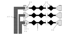
- a transparent electrode pattern 20 for connection with the routing circuit 15 is formed, and a transparent electrode pattern 30 equivalent to the transparent electrode pattern 20 is also provided at the opposite end (the other end) of the strip electrode 5. (See FIGS. 1a, 1b, and 1c).
- the transparent film 2 may be made of any material as long as it is transparent, for example, engineering plastics such as polycarbonate (PC), polyamide, or polyether ketone, acrylic, polyethylene terephthalate (PET), or Polybutylene terephthalate film or the like can be used.
- the thickness of the transparent film 2 is not particularly limited, but is preferably in the range of 20 to 500 ⁇ m in consideration of thinning of the capacitance sensor and stable mass production.
- the strip electrode 5 is composed of a transparent conductive film 11.
- a metal oxide film such as tin oxide, indium oxide, antimony oxide, zinc oxide, cadmium oxide, indium tin oxide (ITO) or antimony-doped tin oxide (ATO), or Composite films mainly composed of these metal oxides, or metals such as gold, silver, copper, tin, nickel, aluminum, or palladium, transparent polymers containing conductive fillers, and conductive materials such as polyethylenedioxythiophene (PEDOT)
- PEDOT polyethylenedioxythiophene
- a method for forming the conductive film for example, a vacuum deposition method, sputtering, ion plating, CVD method, roll coater method, or the like can be used.
- the pattern of the strip electrode 5 may include a series of rhombus electrodes 10 connected along a straight common axis as in Patent Document 1 and Patent Document 2, or a simple electrode having a minimum electrode width of 10 to 200 ⁇ m. It may be a linear pattern. However, as shown in FIG. 1, a transparent electrode pattern 20 for connection to the routing circuit 15 is formed at the end of the strip electrode 5, and the transparent electrode pattern 20 is also formed at the opposite end of the strip electrode 15. A transparent electrode pattern 30 equivalent to the above is provided.
- “equivalent” does not have to be exactly the same, but means that the difference in electrode sensitivity between the transparent electrode pattern 20 and the transparent electrode pattern 30 does not become a problem.
- the transparent electrode pattern 20 at the end is formed by connecting the conventional rhombus electrode pattern 10 to a half triangle 21 of the rhombus electrode pattern 10 and a pattern of a rectangle 22 corresponding to the half area of the rhombus electrode pattern 10.
- the pattern is changed to a transparent electrode pattern 30 similar to the transparent electrode pattern 20 (see FIG. 1a).
- the transparent electrode pattern 20 and the transparent electrode pattern 30 have the same sensitivity as that of the rhombic electrode pattern 10, and the transparent electrode pattern 20 is in a pattern that can be easily electrically connected to the routing circuit 15.
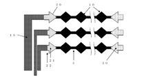
- the transparent electrode pattern 20 and the transparent electrode pattern 30 are not limited to the above-described pattern modes, but may have a pattern such as an arrow (see FIG. 1b) or a square with the conventional rhomboid electrode pattern 10. A pattern (see FIG. 1c) may be used. Further, the transparent electrode pattern 20 and the transparent electrode pattern 30 may have slightly different patterns as long as the difference in electrode sensitivity is not a problem. For example, the transparent electrode pattern 20 shown in FIG. 1 a and the transparent electrode pattern 30 shown in FIG. 1 b can be combined in one strip electrode 5. Alternatively, the transparent electrode 20 and the transparent electrode 30 may have the same area in one band-shaped electrode, and may have different planar shapes as long as the difference in electrode sensitivity does not cause a problem.
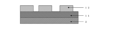
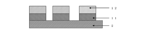
- a transparent conductive film 11 is formed on the entire surface of the transparent film 2 (see FIG. 2a), an etching resist 12 is formed on the transparent conductive film 11 (see FIG. 2b), and the etching is performed.
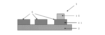
- the transparent conductive film 11 where the resist 12 is not formed is removed by etching (see FIG. 2c), and the etching resist 12 is removed by peeling (see FIG. 2d).
- a routing circuit 15 is formed at one end of the strip electrode 5 (see FIG. 2e).
- etching resist 12 examples include photo-curable or photo-decomposable photosensitive resist materials such as acrylic, polyvinyl cinnamate, synthetic rubber, and novolac, and various printing methods such as gravure and screen, and mask coating. It is formed by the method to do.
- the patterning of the etching resist 12 may be formed using a general-purpose printing method such as gravure printing or screen printing, but in order to correspond to a minimum electrode width of 10 to 200 ⁇ m, a photomask is irradiated with light,
- the method of forming by the photo process of exposing the non-mask part of the etching resist 12 to a desired pattern, and developing is more preferable.
- the etching resist 12 is a photo-curing type
- the development is performed by selectively removing uncured portions by using sodium carbonate or the like as a developer.
- the etching resist 12 is of a photolytic type, it is performed by selectively removing the decomposed portion by using sodium metasilicate as a developer.
- Etching agents include, for example, alkaline etching solutions such as sodium hydroxide, potassium hydroxide, ammonium persulfate, ammonium, ammonium chloride, or cupric chloride, ferric chloride, chromic acid / sulfuric acid mixed solution, hydrogen peroxide solution / sulfuric acid mixed solution.
- An acidic etching solution such as is used.
- the material and the forming method of the routing circuit 15 include a method of forming a conductive paste such as silver paste or carbon paste by a general printing method such as screen printing or gravure printing, and a metal film such as copper is formed by electroless or electrolytic plating. And a method of pattern etching a metal film such as copper formed by a vacuum deposition method or a sputtering method.
- a protective layer or the like may be provided to protect the exposed strip electrode 5.
- a transparent material is selected as the material of the protective layer.
- a transparent plastic film may be bonded or a transparent polymer may be applied.
- a transparent adhesive layer for mounting on a window panel or an LCD panel may also serve as the protective layer.
- a sandwiched frame electrostatic capacitance sensor 100 Is obtained (see FIG. 3).
- the sandwiched frame capacitance sensor 100 is formed by laminating two transparent electrode films 1 so that the strip electrodes 5 are orthogonal to each other.
- a transparent conductive film made of indium tin oxide (ITO) is formed on the entire surface of a 38 ⁇ m-thick polyethylene terephthalate film by a sputtering method, and a photocurable dry film resist is bonded onto the transparent conductive film. Then, ultraviolet light was transmitted through the non-mask portion of the photomask, and the portion corresponding to the strip electrode pattern of the dry film resist was exposed. Next, the exposed dry film resist was developed with sodium carbonate, and the dry film resist in the portion not exposed to light was removed to obtain an etching resist pattern.
- ITO indium tin oxide
- the obtained etching resist pattern has a rhombus shape of a series of 6 mm diagonal lines connected along a common axis of a straight line having a minimum electrode width of 20 ⁇ m except for both end portions, and both end portions are half of the rhombus shape. It was a pattern in which a triangular pattern and a rectangular pattern of 6 mm ⁇ 1.5 m having the same area were connected.
- a transparent electrode film was obtained in the same manner as in Example 1 except that the etching resist pattern at both ends was a rhombus-shaped half-triangle pattern and a pattern like an arrow with a 3 cm square on each side. .
- a transparent electrode film was obtained in the same manner as in Example 1 except that the etching resist pattern on both ends was changed to a pattern in which a rhombus with a diagonal of 6 mm and a square with a side of 3 cm were connected.
- the conductive ink made of silver paste was drawn on one end by screen printing to form a circuit pattern. And 2 sets of them were produced, and as a result of laminating
- the obtained sandwiched frame capacitance sensor operated normally without any imbalance in the sensitivity of the entire transparent electrode.
- Transparent electrode pattern 21 is a half triangular pattern of the conventional rhomboid electrode pattern 30.
- the rectangular pattern is equivalent to the half area of the conventional rhomboid electrode pattern 30.
- Transparent electrode pattern 100 Capacitance sensor with sandwiched frame
Landscapes
- Engineering & Computer Science (AREA)
- General Engineering & Computer Science (AREA)
- Theoretical Computer Science (AREA)
- Human Computer Interaction (AREA)
- Physics & Mathematics (AREA)
- General Physics & Mathematics (AREA)
- Position Input By Displaying (AREA)
- Manufacturing Of Electric Cables (AREA)
- Switches That Are Operated By Magnetic Or Electric Fields (AREA)
Abstract
【課題】透明電極全体の感度にアンバランスが生じない透明電極フィルムを提供する。 【解決手段】透明電極フィルム1は、透明フィルム2の表面に平行に並べられた複数の帯状電極5を有する透明電極フィルム1であって、前記帯状電極5の片側(一方)の端部に引き回し回路15と接続するための透明電極パターン20が形成され、かつ前記帯状電極5の反対側(他方)の端部にも前記透明電極パターン20と同等の透明電極パターン30が設けられている。
Description
本発明は、PDA、ハンディターミナルなど携帯情報端末、コピー機、ファクシミリなどOA機器、スマートフォン、携帯電話機、携帯ゲーム機器、電子辞書、カーナビシステム、小型PC、各種家電品等の静電容量センサなどに用いられる透明電極フィルムに関するものである。
従来、静電容量センサなどに用いられる透明電極フィルムは、中央部に透明電極のパターンが形成され、周囲すなわち額縁に相当する部分に透明電極で得られた電気信号を外部回路に伝える引き回し回路が形成されている。そして、透明電極のパターンは特許文献1や特許文献2に示されるように共通軸に沿って接続された一連の菱形形状の電極を備える帯状電極が複数本平行に並べられた形状をしている場合が多い(特許文献1請求項7、特許文献2図9参照)。一方、静電容量センサは、適用製品の小型化、透明電極部分の大型化による狭額縁化の要望が高く、電気信号の取り出しは片側のみに引き回し回路を設けるようになってきている。
そこで、本発明者らは上記帯状電極と引き回し回路とを確実に接続させるために、位置ずれを考慮して、透明電極の端部を大きくし引き回し回路形成部分まで張り出すようなパターンにした。しかし、そのようにした結果、そこだけ透明電極のパターンが大きくなって透明電極全体の感度にアンバランスが生じる問題が生じた。
そこで、本発明者らは以下の発明により上記課題を解決した。すなわち本発明は、透明フィルムの表面に平行に並べられた複数本の帯状電極を有する透明電極フィルムであって、前記帯状電極の片側の端部に引き回し回路と接続するための透明電極パターンが形成され、かつ前記帯状電極の反対側の端部にも前記透明電極パターンと同等の透明電極パターンが設けられている透明電極フィルムである。
また本発明は、前記帯状電極の片側の端部に設けられた透明電極パターンの一部と引き回し回路のパターンの一部とが積層されている透明電極フィルムであってもよい。また本発明は、透明フィルム上に透明導電膜を全面形成し、前記透明導電膜上にエッチングレジストをパターン形成し、前記エッチングレジストが形成されていない箇所の透明導電膜をエッチング除去し、前記エッチングレジストを剥離除去することにより帯状電極を形成し、前記帯状電極の片側の端部に引き回し回路をパターン形成する透明電極フィルムの製造方法であってもよい。
また本発明は、前記透明電極フィルムと、前記透明電極フィルムの帯状電極と直交する形状の帯状電極を有する第二透明電極フィルムとが積層された挟額縁静電容量センサである。
本発明の透明電極フィルムは、透明フィルムの表面に平行に並べられた複数本の帯状電極を有する透明電極フィルムであって、前記帯状電極の片側の端部に引き回し回路と接続するための透明電極パターンが形成され、かつ前記帯状電極の反対側の端部にも前記透明電極パターンと同等の透明電極パターンが設けられていることを特徴とする。したがって、引き回し回路が形成されている側とそうでない反対側とで透明電極パターンに大差がなく、感度が大して変わらないため、透明電極全体の感度にアンバランスが生じないという効果がある。
また本発明の透明電極フィルムは、前記帯状電極の片側の端部に設けられた透明電極パターンの一部と引き回し回路のパターンの一部とが積層されていることを特徴とする。したがって、帯状電極と引き回し回路パターンとが多少位置ずれを起こしても両者の電気的接続が確実にできるという効果がある。
また本発明の透明電極フィルムの製造方法は、透明フィルム上に透明導電膜を全面形成し、前記透明導電膜上にエッチングレジストをパターン形成し、前記エッチングレジストが形成されていない箇所の透明導電膜をエッチング除去し、前記エッチングレジストを剥離除去することにより帯状電極を形成し、前記帯状電極の片側の端部に引き回し回路をパターン形成することを特徴とする。したがって、狭額縁化の要望に応えられる透明電極フィルムを生産性よく容易に製造できる効果がある。
以下、本発明の透明電極フィルムについて説明する。本発明の透明電極フィルム1は、透明フィルム2の表面に平行に並べられた複数の帯状電極5を有する透明電極フィルム1であって、前記帯状電極5の片側の端部(一方端部)に引き回し回路15と接続するための透明電極パターン20が形成され、かつ前記帯状電極5の反対側の端部(他方端部)にも前記透明電極パターン20と同等の透明電極パターン30が設けられている(図1a、図1b、図1c参照)。
透明フィルム2の材質としては、透明性があるものであればよく、例えば、ポリカーボネート(PC)系、ポリアミド系、若しくはポリエーテルケトン系などのエンジニアリングプラスチック、アクリル系、ポリエチレンテレフタレート(PET)系、又は、ポリブチレンテレフタレート系などのフィルムを用いることができる。透明フィルム2の厚みは特に限定はないが、静電容量センサの薄型化と安定した量産を考慮すると20~500μmの範囲が好ましい。
帯状電極5は透明導電膜11により構成される。当前記透明導電膜11の材料としては、酸化錫、酸化インジウム、酸化アンチモン、酸化亜鉛、酸化カドミウム、インジウムチンオキサイド(ITO)若しくは、アンチモンドープ酸化錫(ATO)などの金属酸化物膜、又は、これらの金属酸化物を主体とする複合膜、又は、金、銀、銅、錫、ニッケル、アルミニウム、若しくは、パラジウムなどの金属、導電フィラー入り透明高分子、ポリエチレンジオキシチオフェン(PEDOT)などの導電性ポリマーの薄膜がある。前記導電膜の形成方法としては、例えば真空蒸着法、スパッタリング、イオンプレーティング、CVD法、ロールコーター法などを用いることができる。
帯状電極5のパターンは、特許文献1や特許文献2のように直線の共通軸に沿って接続された一連の菱形形状の電極10を備えていてもよいし、最小電極幅10~200μmの単なる直線状のパターンであってもよい。ただし図1に示すように、帯状電極5の端部には引き回し回路15と接続するための透明電極パターン20が形成され、かつ前記帯状電極15の反対側の端部にも前記透明電極パターン20と同等の透明電極パターン30が設けられている。ここで同等とは全く同じでなければならないというわけではなく、透明電極パターン20と透明電極パターン30とで電極感度の相違が問題にならない程度にするという意味である。
すなわち、端部の透明電極パターン20は従来の菱形の電極パターン10を、菱形の電極パターン10の半分の三角形21と菱形の電極パターン10の半分の面積に相当する長方形22のパターンとが連なったパターンに変更し、透明電極パターン30も透明電極パターン20と同様のパターンにする(図1a参照)。このようにすることで、透明電極パターン20および透明電極パターン30は菱形の電極パターン10と同じ感度で、透明電極パターン20は引き回し回路15と電気的接続させやすいパターンの態様となる。
なお、透明電極パターン20や透明電極パターン30は上記のパターンの態様に限定されるわけでなく、矢印のようなパターン(図1b参照)にしたり、従来の菱形の電極パターン10と正方形が連なったパターン(図1c参照)などにしたりしてもよい。また、電極感度の相違が問題にならない程度であれば透明電極パターン20と透明電極パターン30とでパターンが多少異なっていても構わない。例えば、図1aで示した透明電極パターン20と図1bで示した透明電極パターン30とを、1つの帯状電極5において組み合わせることができる。あるいは、透明電極20と透明電極30とは、1つの帯状電極において、互いに面積を同一とし、電極感度の相違が問題にならない範囲で互いに平面形状を相違させることもできる。
帯状電極5の製造方法としては、透明フィルム2上に透明導電膜11を全面形成し(図2a参照)、前記透明導電膜11上にエッチングレジスト12をパターン形成し(図2b参照)、前記エッチングレジスト12が形成されていない箇所の透明導電膜11をエッチング除去し(図2c参照)、前記エッチングレジスト12を剥離除去する(図2d参照)方法が挙げられる。そして、帯状電極5の片方の端部に引き回し回路15が形成される(図2e参照)。
エッチングレジスト12としては、アクリル系、ポリビニルシンナメート系、合成ゴム系、ノボラック系などの光硬化型または光分解型の感光性レジスト材料などが挙げられ、グラビア・スクリーンなどの各種印刷方法やマスク塗装する方法などにより形成される。
エッチングレジスト12のパターン化は、グラビア印刷やスクリーン印刷などの汎用印刷方式を用いて形成してもよいが、10~200μmの最小電極幅に対応するために、フォトマスクに光を照射させて、エッチングレジスト12の非マスク部分を所望のパターンに露光し、現像するというフォトプロセスによって形成する方法の方が好ましい。現像は、エッチングレジスト12が光硬化型の場合、炭酸ソーダなどを現像液として使用することにより未硬化部分を選択的に除去することにより行なわれる。またエッチングレジスト12が光分解型の場合、メタケイ酸ソーダなどを現像液として使用することにより分解されている部分を選択的に除去することにより行なわれる。
エッチング剤としては、たとえば水酸化ナトリウム、水酸化カリウム、過硫酸アンモニウム、アンモニウム、塩化アンモニウムなどのアルカリエッチング液または塩化第二銅、塩化第二鉄、クロム酸/硫酸混液、過酸化水素水/硫酸混液などの酸性エッチング液などを用いる。
引き回し回路15の材質および形成方法としては銀ペースト、カーボンペースト等の導電ペーストをスクリーン印刷・グラビア印刷など汎用の印刷法で形成する方法、無電解または電解などのめっきにより銅などの金属膜を形成する方法、真空蒸着法やスパッタリング法で形成した銅などの金属膜をパターンエッチングする方法等が用いられる。
なお、露出した帯状電極5を保護するために保護層等を設けてもよい。保護層の材質は透明な物質が選ばれる。例えば透明プラスチックフィルムを貼り合せたり、透明高分子を塗布してもよい。また、ウインドウパネルやLCDパネルに実装するための透明接着層が前記保護層の役割を兼ねてもよい。
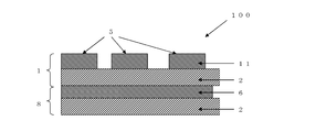
以上の発明によって得られた透明電極フィルム1と、前記透明電極フィルム1の帯状電極5と直交する形状の帯状電極6を有する第二透明電極フィルム8とを積層すれば挟額縁静電容量センサ100が得られる(図3参照)。挟額縁静電容量センサ100は、透明電極フィルム1の2つが、互いの帯状電極5が直交するように積層されている。
厚さ38μmのポリエチレンテレフタレートフィルム上にインジウムスズ酸化物(ITO)からなる透明導電膜をスパッタリング法にて全面形成し、前記透明導電膜上に光硬化型のドライフィルムレジストを貼合し、次に、フォトマスクの非マスク部分に紫外線を透過させて、前記ドライフィルムレジストの帯状電極のパターンに相当する部分を露光した。次いで、前記感光したドライフィルムレジストを炭酸ソーダで現像し、感光しなかった部分のドライフィルムレジストを除去し、エッチングレジストパターンを得た。
得られたエッチングレジストパターンは、両端部以外は最小電極幅20μmの直線とその直線の共通軸に沿って接続された一連の対角線6mmの菱形形状であり、両端部は、前記菱形形状の半分の三角形のパターンと、それと面積を同じくする6mm×1.5mの長方形のパターンが連なったパターンであった。
次に、前記エッチングレジストパターンが形成されていない箇所の透明導電膜を塩化第二鉄でエッチングした後、パターニングされた前記導電膜を被覆するエッチングレジストを3%水酸化ナトリウムで除去した。この工程により、両端部が菱形形状の半分の三角形のパターンと、それと面積を同じくする6mm×1.5mの長方形のパターンが連なったパターンの透明電極フィルムが得られた。
両端部のエッチングレジストパターンを菱形形状の半分の三角形のパターンと、一辺が3cmの正方形が連なった矢印のような形のパターンにした以外は、実施例1と同様にして透明電極フィルムを得た。
両端部のエッチングレジストパターンを対角線6mmの菱形形状と一辺が3cmの正方形が連なったパターンにした以外は、実施例1と同様にして透明電極フィルムを得た。
上記実施例1~実施例3の透明電極フィルムについて、片方の端部に銀ペーストからなる導電インキをスクリーン印刷にて引き回し回路のパターンを形成した。そして、それらを2セット作製し、各帯状電極が直交するように積層した結果、挟額縁静電容量センサが得られた。得られた挟額縁静電容量センサは、透明電極全体の感度にアンバランスが生じるようなこともなく正常に作動するものであった。
1 透明電極フィルム
2 透明フィルム
5 帯状電極
6 帯状電極5と直交する形状の帯状電極
8 第二透明電極フィルム
10 菱形形状の電極
11 透明導電膜
12 エッチングレジスト
15 引き回し回路
20 引き回し回路15と接続するための端部透明電極パターン
21 従来の菱形の電極パターン30の半分の三角形のパターン
22 従来の菱形の電極パターン30の半分の面積に相当する長方形のパターン
30 端部透明電極パターン20と反対側の端部透明電極パターン
100 挟額縁静電容量センサ
2 透明フィルム
5 帯状電極
6 帯状電極5と直交する形状の帯状電極
8 第二透明電極フィルム
10 菱形形状の電極
11 透明導電膜
12 エッチングレジスト
15 引き回し回路
20 引き回し回路15と接続するための端部透明電極パターン
21 従来の菱形の電極パターン30の半分の三角形のパターン
22 従来の菱形の電極パターン30の半分の面積に相当する長方形のパターン
30 端部透明電極パターン20と反対側の端部透明電極パターン
100 挟額縁静電容量センサ
Claims (5)
- 透明フィルムの表面に平行に並べられた複数の帯状電極を有する透明電極フィルムであって、前記帯状電極の片側の端部に引き回し回路と接続するための透明電極パターンが形成され、かつ前記帯状電極の反対側の端部にも前記透明電極パターンと同等の透明電極パターンが形成された、透明電極フィルム。
- 前記帯状電極の両端に形成された前記透明電極パターンの各々は、互いに面積が同一であり、互いに平面形状が相違する、請求項1記載の透明電極フィルム。
- 前記帯状電極の片側の端部に設けられた透明電極パターンの一部と引き回し回路のパターンの一部とが積層されている、請求項1記載の透明電極フィルム。
- 透明フィルム上に透明導電膜を全面形成し、その透明導電膜上にエッチングレジストをパターン形成し、前記エッチングレジストが形成されていない箇所の透明導電膜をエッチング除去し、前記エッチングレジストを剥離除去することにより帯状電極を形成し、前記帯状電極の片側の端部に引き回し回路をパターン形成する、請求項1から3のいずれかに記載の透明電極フィルムの製造方法。
- 請求項1から3のいずれかに記載の透明電極フィルムの2つが、互いの帯状電極が直交するように積層された、狭額縁静電容量センサ。
Priority Applications (1)
| Application Number | Priority Date | Filing Date | Title |
|---|---|---|---|
| JP2012500528A JP5105499B2 (ja) | 2010-02-17 | 2011-01-18 | 透明電極フィルム |
Applications Claiming Priority (2)
| Application Number | Priority Date | Filing Date | Title |
|---|---|---|---|
| JP2010-032046 | 2010-02-17 | ||
| JP2010032046 | 2010-02-17 |
Publications (1)
| Publication Number | Publication Date |
|---|---|
| WO2011102168A1 true WO2011102168A1 (ja) | 2011-08-25 |
Family
ID=44482770
Family Applications (1)
| Application Number | Title | Priority Date | Filing Date |
|---|---|---|---|
| PCT/JP2011/050715 Ceased WO2011102168A1 (ja) | 2010-02-17 | 2011-01-18 | 透明電極フィルム |
Country Status (3)
| Country | Link |
|---|---|
| JP (1) | JP5105499B2 (ja) |
| TW (1) | TW201205600A (ja) |
| WO (1) | WO2011102168A1 (ja) |
Cited By (3)
| Publication number | Priority date | Publication date | Assignee | Title |
|---|---|---|---|---|
| JP2012189870A (ja) * | 2011-03-11 | 2012-10-04 | Dainippon Printing Co Ltd | 積層パターン基板の製造方法およびタッチパネルセンサの製造方法 |
| JP2014056578A (ja) * | 2012-09-13 | 2014-03-27 | Rtr-Tech Technology Co Ltd | タッチパネル及びその製造方法 |
| WO2018062372A1 (ja) * | 2016-09-29 | 2018-04-05 | 積水化学工業株式会社 | 光透過性導電フィルム及びパターン状の導電層を有する光透過性導電フィルムの製造方法 |
Families Citing this family (1)
| Publication number | Priority date | Publication date | Assignee | Title |
|---|---|---|---|---|
| KR102354247B1 (ko) | 2017-04-24 | 2022-01-24 | 삼성디스플레이 주식회사 | 표시모듈 |
Citations (1)
| Publication number | Priority date | Publication date | Assignee | Title |
|---|---|---|---|---|
| JP2009015489A (ja) * | 2007-07-03 | 2009-01-22 | Hitachi Displays Ltd | タッチパネル付き表示装置 |
Family Cites Families (9)
| Publication number | Priority date | Publication date | Assignee | Title |
|---|---|---|---|---|
| JP5060845B2 (ja) * | 2007-06-27 | 2012-10-31 | 株式会社ジャパンディスプレイイースト | 画面入力型画像表示装置 |
| KR100921813B1 (ko) * | 2007-11-07 | 2009-10-16 | 주식회사 애트랩 | 터치 패널 장치 및 이의 접촉위치 검출방법 |
| JP4945483B2 (ja) * | 2008-02-27 | 2012-06-06 | 株式会社 日立ディスプレイズ | 表示パネル |
| JP5207808B2 (ja) * | 2008-04-15 | 2013-06-12 | 株式会社ジャパンディスプレイイースト | 入力装置、及びそれを備えた表示装置 |
| JP5103254B2 (ja) * | 2008-04-16 | 2012-12-19 | 株式会社ジャパンディスプレイイースト | 静電容量方式タッチパネルおよびそれを備える画面入力型表示装置 |
| JP5133791B2 (ja) * | 2008-06-19 | 2013-01-30 | 株式会社ジャパンディスプレイイースト | タッチパネル付き表示装置 |
| JP5075082B2 (ja) * | 2008-10-06 | 2012-11-14 | 株式会社ジャパンディスプレイイースト | 入力装置、及びそれを備えた表示装置 |
| JP2010108038A (ja) * | 2008-10-28 | 2010-05-13 | Hitachi Displays Ltd | タッチパネル及びその製造方法並びにタッチパネル表示装置 |
| KR101048980B1 (ko) * | 2009-01-16 | 2011-07-12 | 삼성모바일디스플레이주식회사 | 터치 스크린 패널 및 그 제조방법 |
-
2011
- 2011-01-18 WO PCT/JP2011/050715 patent/WO2011102168A1/ja not_active Ceased
- 2011-01-18 JP JP2012500528A patent/JP5105499B2/ja active Active
- 2011-02-16 TW TW100105012A patent/TW201205600A/zh unknown
Patent Citations (1)
| Publication number | Priority date | Publication date | Assignee | Title |
|---|---|---|---|---|
| JP2009015489A (ja) * | 2007-07-03 | 2009-01-22 | Hitachi Displays Ltd | タッチパネル付き表示装置 |
Cited By (5)
| Publication number | Priority date | Publication date | Assignee | Title |
|---|---|---|---|---|
| JP2012189870A (ja) * | 2011-03-11 | 2012-10-04 | Dainippon Printing Co Ltd | 積層パターン基板の製造方法およびタッチパネルセンサの製造方法 |
| JP2014056578A (ja) * | 2012-09-13 | 2014-03-27 | Rtr-Tech Technology Co Ltd | タッチパネル及びその製造方法 |
| WO2018062372A1 (ja) * | 2016-09-29 | 2018-04-05 | 積水化学工業株式会社 | 光透過性導電フィルム及びパターン状の導電層を有する光透過性導電フィルムの製造方法 |
| KR20190065187A (ko) * | 2016-09-29 | 2019-06-11 | 세키스이가가쿠 고교가부시키가이샤 | 광 투과성 도전 필름 및 패턴형의 도전층을 갖는 광 투과성 도전 필름의 제조 방법 |
| KR102446081B1 (ko) * | 2016-09-29 | 2022-09-22 | 세키스이가가쿠 고교가부시키가이샤 | 광 투과성 도전 필름 및 패턴형의 도전층을 갖는 광 투과성 도전 필름의 제조 방법 |
Also Published As
| Publication number | Publication date |
|---|---|
| TW201205600A (en) | 2012-02-01 |
| JP5105499B2 (ja) | 2012-12-26 |
| JPWO2011102168A1 (ja) | 2013-06-17 |
Similar Documents
| Publication | Publication Date | Title |
|---|---|---|
| JP5383991B2 (ja) | 静電容量センサとその製造方法 | |
| JP4601710B1 (ja) | 狭額縁タッチ入力シートとその製造方法 | |
| JP5298209B2 (ja) | 静電容量式センサーシートおよびその製造方法 | |
| TWI484381B (zh) | Touch panel and manufacturing method thereof | |
| KR101313028B1 (ko) | 커버 유리 일체형 센서 | |
| CN104246676B (zh) | 触摸面板构件以及其制造方法 | |
| WO2011162221A1 (ja) | 防錆性に優れた狭額縁タッチ入力シートとその製造方法 | |
| JP5026581B2 (ja) | カバーガラス一体型センサー | |
| JP5105499B2 (ja) | 透明電極フィルム | |
| CN107450777A (zh) | 一种触控基板及其制备方法、触控面板、显示装置 | |
| US10951211B2 (en) | FPC integrated capacitance switch and method of manufacturing the same | |
| CN111722742A (zh) | 透明导电膜及其制备方法 | |
| JP2013251220A (ja) | 導電パターン形成基板の製造方法および導電パターン形成基板 | |
| JP2011129272A (ja) | 両面透明導電膜シートとその製造方法 | |
| JP6457897B2 (ja) | タッチ入力センサ及びその製造方法 | |
| JP2014029682A (ja) | タッチパネル | |
| JP2011065394A (ja) | 保護フィルム付き狭額縁タッチ入力シート、保護フィルム付き積層狭額縁タッチ入力シート及びこれらの製造方法 | |
| JP4870830B2 (ja) | 防錆性に優れた両面透明導電膜シートとその製造方法 | |
| KR101551859B1 (ko) | 금속 레이어를 에칭 레지스트로 이용하는 에칭 방법 | |
| TW201419108A (zh) | 透明導電圖樣之形成方法、觸摸屏之製造方法和導電轉印膜 | |
| KR101428009B1 (ko) | 터치 패널 및 제조 방법 | |
| JP6129611B2 (ja) | タッチパネルの製造方法 | |
| JP2015106264A (ja) | 配線フィルム製造用フォトマスク及び配線フィルムの製造方法 | |
| CN102981668A (zh) | 触摸面板 | |
| JP2013180918A (ja) | ガラス基板の製造方法、電極パターン付きガラス基板の製造方法 |
Legal Events
| Date | Code | Title | Description |
|---|---|---|---|
| 121 | Ep: the epo has been informed by wipo that ep was designated in this application |
Ref document number: 11744457 Country of ref document: EP Kind code of ref document: A1 |
|
| WWE | Wipo information: entry into national phase |
Ref document number: 2012500528 Country of ref document: JP |
|
| NENP | Non-entry into the national phase |
Ref country code: DE |
|
| 122 | Ep: pct application non-entry in european phase |
Ref document number: 11744457 Country of ref document: EP Kind code of ref document: A1 |