WO2011102135A1 - 半導体装置の製造方法及び製造装置 - Google Patents
半導体装置の製造方法及び製造装置 Download PDFInfo
- Publication number
- WO2011102135A1 WO2011102135A1 PCT/JP2011/000887 JP2011000887W WO2011102135A1 WO 2011102135 A1 WO2011102135 A1 WO 2011102135A1 JP 2011000887 W JP2011000887 W JP 2011000887W WO 2011102135 A1 WO2011102135 A1 WO 2011102135A1
- Authority
- WO
- WIPO (PCT)
- Prior art keywords
- pattern
- photoresist
- manufacturing
- pitch
- semiconductor device
- Prior art date
- Legal status (The legal status is an assumption and is not a legal conclusion. Google has not performed a legal analysis and makes no representation as to the accuracy of the status listed.)
- Ceased
Links
Images

Classifications
-
- H—ELECTRICITY
- H10—SEMICONDUCTOR DEVICES; ELECTRIC SOLID-STATE DEVICES NOT OTHERWISE PROVIDED FOR
- H10W—GENERIC PACKAGES, INTERCONNECTIONS, CONNECTORS OR OTHER CONSTRUCTIONAL DETAILS OF DEVICES COVERED BY CLASS H10
- H10W20/00—Interconnections in chips, wafers or substrates
- H10W20/01—Manufacture or treatment
- H10W20/071—Manufacture or treatment of dielectric parts thereof
- H10W20/081—Manufacture or treatment of dielectric parts thereof by forming openings in the dielectric parts
- H10W20/089—Manufacture or treatment of dielectric parts thereof by forming openings in the dielectric parts using processes for implementing desired shapes or dispositions of the openings, e.g. double patterning
-
- H—ELECTRICITY
- H10—SEMICONDUCTOR DEVICES; ELECTRIC SOLID-STATE DEVICES NOT OTHERWISE PROVIDED FOR
- H10P—GENERIC PROCESSES OR APPARATUS FOR THE MANUFACTURE OR TREATMENT OF DEVICES COVERED BY CLASS H10
- H10P50/00—Etching of wafers, substrates or parts of devices
- H10P50/73—Etching of wafers, substrates or parts of devices using masks for insulating materials
-
- H—ELECTRICITY
- H10—SEMICONDUCTOR DEVICES; ELECTRIC SOLID-STATE DEVICES NOT OTHERWISE PROVIDED FOR
- H10P—GENERIC PROCESSES OR APPARATUS FOR THE MANUFACTURE OR TREATMENT OF DEVICES COVERED BY CLASS H10
- H10P76/00—Manufacture or treatment of masks on semiconductor bodies, e.g. by lithography or photolithography
- H10P76/20—Manufacture or treatment of masks on semiconductor bodies, e.g. by lithography or photolithography of masks comprising organic materials
- H10P76/204—Manufacture or treatment of masks on semiconductor bodies, e.g. by lithography or photolithography of masks comprising organic materials of organic photoresist masks
-
- H—ELECTRICITY
- H10—SEMICONDUCTOR DEVICES; ELECTRIC SOLID-STATE DEVICES NOT OTHERWISE PROVIDED FOR
- H10P—GENERIC PROCESSES OR APPARATUS FOR THE MANUFACTURE OR TREATMENT OF DEVICES COVERED BY CLASS H10
- H10P76/00—Manufacture or treatment of masks on semiconductor bodies, e.g. by lithography or photolithography
- H10P76/20—Manufacture or treatment of masks on semiconductor bodies, e.g. by lithography or photolithography of masks comprising organic materials
- H10P76/204—Manufacture or treatment of masks on semiconductor bodies, e.g. by lithography or photolithography of masks comprising organic materials of organic photoresist masks
- H10P76/2041—Photolithographic processes
-
- H—ELECTRICITY
- H10—SEMICONDUCTOR DEVICES; ELECTRIC SOLID-STATE DEVICES NOT OTHERWISE PROVIDED FOR
- H10P—GENERIC PROCESSES OR APPARATUS FOR THE MANUFACTURE OR TREATMENT OF DEVICES COVERED BY CLASS H10
- H10P76/00—Manufacture or treatment of masks on semiconductor bodies, e.g. by lithography or photolithography
- H10P76/40—Manufacture or treatment of masks on semiconductor bodies, e.g. by lithography or photolithography of masks comprising inorganic materials
- H10P76/408—Manufacture or treatment of masks on semiconductor bodies, e.g. by lithography or photolithography of masks comprising inorganic materials characterised by their sizes, orientations, dispositions, behaviours or shapes
- H10P76/4085—Manufacture or treatment of masks on semiconductor bodies, e.g. by lithography or photolithography of masks comprising inorganic materials characterised by their sizes, orientations, dispositions, behaviours or shapes characterised by the processes involved to create the masks
-
- H—ELECTRICITY
- H10—SEMICONDUCTOR DEVICES; ELECTRIC SOLID-STATE DEVICES NOT OTHERWISE PROVIDED FOR
- H10P—GENERIC PROCESSES OR APPARATUS FOR THE MANUFACTURE OR TREATMENT OF DEVICES COVERED BY CLASS H10
- H10P76/00—Manufacture or treatment of masks on semiconductor bodies, e.g. by lithography or photolithography
- H10P76/40—Manufacture or treatment of masks on semiconductor bodies, e.g. by lithography or photolithography of masks comprising inorganic materials
- H10P76/408—Manufacture or treatment of masks on semiconductor bodies, e.g. by lithography or photolithography of masks comprising inorganic materials characterised by their sizes, orientations, dispositions, behaviours or shapes
- H10P76/4088—Processes for improving the resolution of the masks
Definitions
- the present invention relates to a semiconductor device manufacturing method and a manufacturing apparatus.
- a fine circuit pattern is formed by a photolithography technique using a photoresist.
- SWT side wall transfer
- DP double patterning
- a technique in which a photoresist pattern formed first is transferred to a hard mask, and the hard mask and the resist mask are used.
- the pattern is once transferred to the hard mask in this way, formation of the hard mask layer, etching of the hard mask layer, and the like are required, which increases the number of processes.
- the photoresist pattern is frozen (insolubilized), and then the second photoresist pattern is formed (photoresist application, exposure, development).
- a technique is known in which etching is performed using the double photoresist pattern as a mask after performing the lithography process twice (see, for example, Patent Document 1).
- a V-LINE is formed by the first exposure in the first step, and then V-LINE is formed in the second step.
- the orthogonal pattern obtained by forming the orthogonal H-LINE in the second exposure is transferred to the hard mask once, and the target pattern is formed in the third step to form holes at the target location.
- the fine random holes were obtained on the substrate for the first time after transferring to the hard mask.
- the present invention has been made in response to the above-described circumstances, and provides a method and apparatus for manufacturing a semiconductor device that eliminates the first step of transferring to a hard mask and improves production efficiency. It is what.
- One embodiment of a method for manufacturing a semiconductor device includes a step of forming a mask layer on an etching target layer formed on a substrate and etching the etching target layer using the mask layer as a mask.
- a semiconductor includes a step of forming a mask layer on an etching target layer formed on a substrate and etching the etching target layer using the mask layer as a mask.
- a method for manufacturing an apparatus comprising: forming a first photoresist layer on the substrate, exposing and developing the first photoresist pattern to form a first photoresist pattern; and insolubilizing the first photoresist pattern.
- 1 insolubilization step forming a second photoresist layer on the first photoresist pattern, exposing and developing to form a second photoresist pattern intersecting with the first photoresist pattern A forming step, a second insolubilizing step for insolubilizing the second photoresist pattern, the first photoresist pattern and the second photoresist pattern.
- On the O DOO resist pattern forming a third photoresist layer, exposed and developed, and a third pattern formation step of forming a third photoresist pattern, by and forming the mask layer.
- a step of transferring a first parallel pattern to a photoresist applied on a substrate, and a direction orthogonal to the first parallel pattern to the photoresist A step of transferring a second parallel pattern to be transferred, and a step of transferring a pattern corresponding to a hole of a third predetermined random pattern to the photoresist.
- a step of transferring a first parallel pattern to a photoresist applied on a substrate and a step parallel to the first parallel pattern to the photoresist.
- a step of transferring a pattern corresponding to a hole of a third predetermined random pattern to the photoresist is provided.
- the manufacturing method and manufacturing apparatus of a semiconductor device which can reduce the number of processes compared with the past, can form a fine pattern efficiently, and can improve production efficiency can be provided. .
- FIG. 2 is a flowchart showing a process of a manufacturing method of the semiconductor device of FIG.
- the top view which shows the structure of the manufacturing apparatus of the semiconductor device which concerns on one Embodiment of this invention.
- FIG. 4 is a rear view showing the configuration of the semiconductor device manufacturing apparatus of FIG. 3.
- FIG. 1 schematically shows an enlarged part of a semiconductor wafer as a substrate according to an embodiment of the present invention, and shows steps of a method for manufacturing a semiconductor device according to the embodiment.
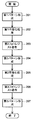
- FIG. 2 is a flowchart showing the steps of the semiconductor device manufacturing method according to the embodiment.
- an insulating film (for example, a TEOS film) 101, a hard mask 102, and an antireflection film 103 are formed in this order on the semiconductor wafer 100 from the lower side.
- a photoresist is applied on the antireflection film 103, and exposure and development are performed to form a first photoresist pattern 104 having a line-and-space shape (step 201 in FIG. 2).
- the shape of the 1st photoresist pattern 104 seen from the upper surface is typically shown in the upper part of FIG.
- the line width of the first photoresist pattern 104 is, for example, about 40 nm to 50 nm, and the pitch is, for example, about 80 nm to 100 nm (half pitch is, for example, about 40 nm to 50 nm).
- the formation of can be performed, for example, by ArF immersion exposure.
- a first insolubilization process (first freezing process) is performed to insolubilize the first photoresist pattern 104 to form an insolubilized layer 104a (step 202 in FIG. 2).
- This first insolubilization treatment can be performed, for example, by chemical freezing.
- a second photoresist 105 is applied on the first photoresist pattern 104 (step 203 in FIG. 2).
- a second photoresist pattern 106 having a line-and-space shape (step 204 in FIG. 2).
- the first photoresist pattern 104 and the second photoresist pattern 106 are formed so as to intersect at right angles.
- a second insolubilization process (second freezing process) is performed to insolubilize the second photoresist pattern 106 to form an insolubilized layer 106a (step 205 in FIG. 2).
- This second insolubilization treatment can be performed by chemical freezing, for example.
- a third photoresist 107 is applied on the first photoresist pattern 104 and the second photoresist pattern 106 (step 206 in FIG. 2).
- the third photoresist pattern 108 is a random pattern, and is based on the first photoresist pattern 104 and the second photoresist pattern 106.
- the pattern is formed at a wide pitch.
- a mask having a pattern in which contact holes arranged at a narrow pitch and holes having a random shape formed at a pitch wider than these contact holes can be formed.
- the lower antireflection film 103 and the hard mask 102 are etched, and further, the insulating film (eg, TEOS film) 101 is etched to form holes in the insulating film (eg, TEOS film) 101.
- a pattern is temporarily transferred to a hard mask in the middle, and a photoresist mask is not formed again on the hard mask, but a mask made of a three-layer photoresist pattern is used.
- the contact holes are closely arranged with a line width of about 40 to 50 nm and a pitch of about 80 to 100 nm (half pitch is about 40 to 50 nm), and a pitch of about 160 to 200 nm wider than these contact holes.
- the dimensional pattern can be transferred at a time. Therefore, the number of steps can be reduced as compared with the conventional case, and a fine pattern can be efficiently formed, and the production efficiency can be improved.
- the first photoresist pattern 104 has a line-and-space shape with a pitch of about 80 to 100 nm
- the second photoresist pattern 106 has a line-and-space shape orthogonal to this with the same pitch as the first photoresist pattern. Therefore, it is possible to form closely aligned contact holes with a pitch of about 80 to 100 nm without requiring fine alignment. Thereafter, only a predetermined contact hole among the closely aligned contact holes can be left by a third photoresist pattern having a pitch of about 160 to 200 nm wider than the first photoresist pattern and the second photoresist pattern. Therefore, it is not necessary to use the minimum resolution for all patterns, and a contact hole having a predetermined shape can be formed by three simple exposures of a pattern having a minimum pitch of 2 times and a pattern having a pitch wider than that.
- the first photoresist pattern is a pattern in which holes are aligned.
- the second photoresist pattern having a pattern in which holes are arranged between these holes precise alignment is required, and the possibility that the positions of the holes are shifted increases.
- the first photoresist pattern 104 and the second photoresist pattern 106 have orthogonal line-and-space shapes with the same pitch, but these pitches may not be equal and the patterns are orthogonal. Not necessary.
- a closely aligned hole-shaped pattern can be used in the step of forming a closely aligned hole pattern. In this case, not the method of crossing the line-and-space pattern as in the present embodiment, but a hole-shaped photoresist pattern that is closely aligned is formed by one exposure and development, and then the present embodiment A random hole pattern can be formed by the same procedure as in FIG.
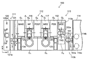
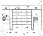
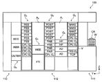
- FIG. 3 to 5 schematically show the configuration of a resist coating / development processing system as a semiconductor device manufacturing apparatus according to this embodiment.
- FIG. 3 is a plan view
- FIG. 4 is a front view
- FIG. It is a rear view.
- the resist coating / development processing system 100 transfers a semiconductor wafer W between a cassette station 111, a processing station 112 having a plurality of processing units, and an exposure apparatus 114 and a processing station 112 provided adjacent to the processing station 112. And an interface station 113 for delivery.
- a wafer cassette (CR) in which a plurality of semiconductor wafers W to be processed in the resist coating / development processing system 100 is horizontally stored is carried from another system.
- the wafer cassette (CR) containing the semiconductor wafer W that has been processed in the resist coating / development processing system 100 is unloaded from the cassette station 111 to another system.
- the cassette station 111 carries the semiconductor wafer W between the wafer cassette (CR) and the processing station 112.
- a cassette mounting table 120 extending along the X direction is provided at the inlet side end (Y direction end in FIG. 3) of the cassette station 111.
- a plurality of (five in FIG. 3) positioning projections 120a are arranged in a line along the X direction on the cassette mounting table 120, and the wafer cassette (CR) faces the wafer loading / unloading port toward the processing station 112 side.
- the lever is placed at the position of the protrusion 120a.
- a wafer transfer mechanism 121 is provided so as to be positioned between the cassette mounting table 120 and the processing station 112.
- the wafer transfer mechanism 121 includes a wafer transfer pick 121a that can move in the cassette arrangement direction (X direction) and the arrangement direction (Z direction) of the semiconductor wafers W in the wafer cassette (CR).
- the pick 121a is rotatable in the ⁇ direction shown in FIG. Thereby, the wafer transfer pick 121a can access any wafer cassette (CR), and is provided with a transition unit (TRS-G 3) provided in a third processing unit group G 3 of the processing station 112 described later. ) Can be accessed.
- TRS-G 3 transition unit
- the processing station 112 the system front side, in order from the cassette station 111 side, the first processing unit group G 1 and the second processing unit group G 2 is arranged. Further, a third processing unit group G 3 , a fourth processing unit group G 4 and a fifth processing unit group G 5 are arranged on the system rear side in order from the cassette station 111 side.
- the first main transfer section A 1 is disposed between the third processing unit group G 3 and the fourth processing unit group G 4, and the fourth processing unit group G 4 and the fifth processing unit group G 5 the second main transfer section a 2 is disposed between.
- the first main rear side of the transport unit A 1 sixth processing unit group G 6 is provided, on the back side of the second main transfer section A 2 is disposed seventh processing unit group G 7 Yes.
- the first processing unit group G 1 includes five spinner type processing units as liquid supply units that perform predetermined processing by placing a semiconductor wafer W on a spin chuck in a cup, For example, three photoresist coating units (COT) and two coating units (BARC) for forming an antireflection film for preventing reflection of light during exposure are arranged in a total of five stages.
- COT photoresist coating units
- BARC coating units
- 5 spinner-type processing units for example, chemical freezing unit for implementing a chemical freezing as insolubilization process described above (CHF) and four developing units (DEV) are five stages Are arranged to overlap each other.
- the third processing unit group G 3 includes, from below, a temperature control unit (TCP), a transfer unit for the semiconductor wafer W between the cassette station 111 and the first main transfer unit A 1. Transition unit (TRS-G 3 ), a spare space V in which a desired oven-type processing unit and the like can be provided, and three high-precision temperature control units that heat-treat the semiconductor wafer W under accurate temperature control ( CPL-G 3 ) and four high-temperature heat treatment units (BAKE) for performing predetermined heat treatment on the semiconductor wafer W are arranged in a total of 10 stages.
- TCP temperature control unit
- TRS-G 3 transition unit
- CPL-G 3 three high-precision temperature control units that heat-treat the semiconductor wafer W under accurate temperature control
- BAKE high-temperature heat treatment units
- the fourth processing unit group G 4 includes, from below, a high-precision temperature control unit (CPL-G 4 ), four pre-baking units (PAB) that heat-treat the semiconductor wafer W after resist coating, and development processing.
- CPL-G 4 high-precision temperature control unit
- PAB pre-baking units
- POST post bake units
- the fifth processing unit group G 5 includes four high-precision temperature control units (CPL-G 5 ) and six post-exposure baking units that heat-treat the semiconductor wafer W after exposure and before development, from the bottom. (PEB) are arranged in a total of 10 stages.
- the high temperature heat treatment units (BAKE), pre-bake units (PAB), post-bake units (POST), and post-exposure bake units (PEB) provided in the third to fifth processing unit groups G 3 to G 5 are, for example, all It has the same structure and constitutes a heat treatment unit.
- the number of stacked stages and the arrangement of units of the third to fifth processing unit groups G 3 to G 5 are not limited to those shown in the figure, and can be arbitrarily set.
- the seventh processing unit group G 7 includes, from below, a film thickness measuring device (FTI) that measures the resist film thickness and a peripheral exposure device (WEE) that selectively exposes only the edge portion of the semiconductor wafer W. It is arranged on the steps.
- FTI film thickness measuring device
- WEE peripheral exposure device
- the first main transfer section A 1 is provided first main wafer transfer device 116, the first main wafer transfer device 116, the first processing unit group G 1, the third processing unit group Each unit included in G 3 , the fourth processing unit group G 4 and the sixth processing unit group G 6 can be selectively accessed.
- the second main transfer section A 2 is provided a second main wafer transfer device 117, the second main wafer transfer device 117, the second processing unit group G 2, the fourth processing unit group G 4, the fifth processing unit
- Each unit provided in the group G 5 and the seventh processing unit group G 7 can be selectively accessed.
- the semiconductor wafer W is held on these arms and is transported in each of the X direction, the Y direction, the Z direction, and the ⁇ direction.
- a liquid temperature adjusting pump 124 and a duct 128 are provided between the first processing unit group G 1 and the cassette station 111, and between the second processing unit group G 2 and the interface station 113.
- a liquid temperature adjusting pump 125 and a duct 129 are provided. Liquid temperature adjusting pump 124 and 125, and supplies a predetermined processing liquid first processing unit group G 1 respectively to the second processing unit group G 2.
- the ducts 128 and 129 are for supplying clean air from an air conditioner (not shown) provided outside the resist coating / development processing system 100 to the inside of each of the processing unit groups G 1 to G 5 .
- the first processing unit group G 1 to the seventh processing unit group G 7 can be removed for maintenance, and the panel on the back side of the processing station 112 can be removed or opened / closed. Further, as shown in FIG. 4, the first processing unit group G 1 of the lower second processing unit group G 2, the first processing unit group G 1 and a predetermined process liquid to the second processing unit group G 2 Supplying chemical units (CHM) 126 and 127 are provided.
- CHM chemical units
- Interface station 113 includes a first interface station 113a of the processing station 112 side, and is composed of a second interface station 113b of the exposure apparatus 114 side, the first interface station 113a opening in the fifth processing unit group G 5
- a first wafer transfer body 162 is disposed so as to face the part, and a second wafer transfer body 163 movable in the X direction is disposed at the second interface station 113b.
- in buffer cassette for temporarily accommodating the semiconductor wafer W to be (INBR) eighth processing unit group G 8 to the edge exposure unit (WEE) is constituted by stacking is disposed.
- the in buffer cassette (INBR) and the out buffer cassette (OUTBR) can accommodate a plurality of, for example, 25 semiconductor wafers W.
- a two-stage high-precision temperature control unit (CPL-G 9 ), a transition unit (TRS-G 9 ), and ninth processing unit group G 9 is arranged which is configured by stacking.
- the first wafer transfer body 162 has a wafer fork 162a that can move in the Z direction and rotate in the ⁇ direction, and that can advance and retreat in the XY plane. .
- the fork 162a can selectively access each of the fifth processing unit group G 5 , the eighth processing unit group G 8 , and the ninth processing unit group G 9 .
- the semiconductor wafer W can be transferred.
- the second wafer transfer body 163 has a fork 163a for wafer transfer that can move in the X and Z directions, can rotate in the ⁇ direction, and can advance and retreat in the XY plane.
- the fork 163a includes units of the ninth processing unit group G 9, being selectively accessible against incoming stage 114a and outgoing stage 114b of the exposure apparatus 114, the transfer of the semiconductor wafers W between these portions Can be done.
- the central control unit 119 includes a process controller including a CPU that controls each unit of the resist coating / development processing system 100 and each component such as each transport mechanism, a user interface including a keyboard and a display, a control program, A storage unit storing recipes, various databases, and the like.
- the first to third resist pattern forming steps described above are performed as follows.
- the semiconductor wafer W before processing from the wafer cassette (CR) is taken out by the wafer transfer mechanism 121 one by one, the semiconductor wafer W to the processing station 112 of the processing unit group G 3 in placed transit unit (TRS-G 3 ).
- the baking process in the high temperature heat treatment unit (BAKE) is performed.
- an adhesion process may be performed by the adhesion unit (AD).
- the semiconductor wafer W is transferred to the resist coating unit (COT) belonging to the first processing unit group G 1 , and photo A resist coating process is performed.
- COT resist coating unit
- the semiconductor wafer W is transferred into the exposure apparatus 114 by the second wafer transfer body 163.
- the semiconductor wafer W that has been subjected to the exposure process by the exposure apparatus 114 is carried into the transition unit (TRS-G 9 ) by the second wafer transfer body 163. Thereafter, the semiconductor the wafer W, post-exposure baking treatment by post-exposure baking unit (PEB) which belongs to the fifth processing unit group G 5, the developing process by the developing unit (DEV) belonging to the second processing unit group G 2, post-baking Temperature control processing such as post-baking processing by the unit (POST) is performed.
- PEB post-exposure baking treatment by post-exposure baking unit
- DEV developing process by the developing unit (DEV) belonging to the second processing unit group G 2
- post-baking Temperature control processing such as post-baking processing by the unit (POST) is performed.
- the first photoresist pattern is patterned by the above procedure. Then, to convey the semiconductor wafer W in the chemical freezing unit (CHF) belonging to the second processing unit group G 2, it performs the insolubilization treatment here.
- CHF chemical freezing unit
- a second photoresist pattern is formed by repeating steps from the photoresist coating process by the resist coating unit (COT) to the insolubilization process by the chemical freezing unit (CHF). Further, a third photoresist pattern is formed by repeating the steps from the photoresist coating process by the resist coating unit (COT) to the temperature control process such as the post baking process by the post bake unit (POST). Etching is performed using these first to third photoresist patterns as a mask.
- the present invention can be used in the field of manufacturing semiconductor devices. Therefore, it has industrial applicability.
- DESCRIPTION OF SYMBOLS 100 ... Semiconductor wafer, 101 ... Insulating film (TEOS film), 102 ... Hard mask, 103 ... Antireflection film (BARC), 104 ... First photoresist pattern, 104a ... Insolubilized layer, 105 ... First 2 photoresist, 106... Second photoresist pattern, 106 a... Insolubilized layer, 107... Third photoresist, 108.
- TEOS film Insulating film
- BARC Antireflection film
Landscapes
- Exposure Of Semiconductors, Excluding Electron Or Ion Beam Exposure (AREA)
- Exposure And Positioning Against Photoresist Photosensitive Materials (AREA)
- Photosensitive Polymer And Photoresist Processing (AREA)
Abstract
Description
Claims (15)
- 基板上に形成された被エッチング層の上部にマスク層を形成し、当該マスク層をマスクとして前記被エッチング層のエッチングを行う工程を有する半導体装置の製造方法であって、
前記基板に第1フォトレジスト層を形成する第1フォトレジスト層形成工程と、
前記第1フォトレジスト層に、第1のピッチで整列したホール形状の第1フォトレジストパターンを形成する第1フォトレジストパターン形成工程と、
前記第1フォトレジストパターンを不溶化する不溶化工程と、
前記第1フォトレジストパターンの上に、第2フォトレジスト層を形成する第2フォトレジスト層形成工程と、
前記第2フォトレジスト層に、前記第1のピッチより広い第2のピッチのパターンを形成する第2フォトレジストパターン形成工程と、
によって前記マスク層を形成することを特徴とする半導体装置の製造方法。 - 請求項1記載の半導体装置の製造方法であって、
前記第1のピッチは80~100nmであり、
前記第2のピッチは160~200nmである
ことを特徴とする半導体の製造方法。 - 請求項1又は2記載の半導体装置の製造方法であって、
前記第1のピッチで整列したホール形状のパターンが真円または楕円である
ことを特徴とする半導体の製造方法。 - 基板上に形成された被エッチング層の上部にマスク層を形成し、当該マスク層をマスクとして前記被エッチング層のエッチングを行う工程を有する半導体装置の製造方法であって、
前記基板に第1フォトレジスト層を形成し、露光、現像して第1フォトレジストパターンを形成する第1パターン形成工程と、
前記第1フォトレジストパターンを不溶化する第1不溶化工程と、
前記第1フォトレジストパターンの上に、第2フォトレジスト層を形成し、露光、現像して、前記第1フォトレジストパターンと交差する第2フォトレジストパターンを形成する第2パターン形成工程と、
前記第2フォトレジストパターンを不溶化する第2不溶化工程と、
前記第1フォトレジストパターン及び前記第2フォトレジストパターンの上に、第3フォトレジスト層を形成し、露光、現像して、第3フォトレジストパターンを形成する第3パターン形成工程と、
によって前記マスク層を形成することを特徴とする半導体装置の製造方法。 - 請求項4記載の半導体装置の製造方法であって、
前記第1パターン形成工程と、前記第2パターン形成工程とによって、第1のピッチで整列したホール形状のパターンを形成し、
前記第3パターン形成工程によって、前記第1のピッチより広い第2のピッチのパターンを形成する
ことを特徴とする半導体装置の製造方法。 - 請求項5記載の半導体装置の製造方法であって、
前記第1のピッチは80~100nmであり、
前記第2のピッチは160~200nmである
ことを特徴とする半導体装置の製造方法。 - 基板上に塗布されたフォトレジストに、第1の平行したパターンを転写する工程と、
前記フォトレジストに、前記第1の平行したパターンと直交する第2の平行したパターンを転写する工程と、
前記フォトレジストに、第3の予め定められたランダムパターンのホールに対応したパターンを転写する工程と
を備えたことを特徴とする半導体装置の製造方法。 - 請求項7記載の半導体装置の製造方法であって、
前記第1の平行したパターンのピッチは80~100nmであり、
前記第2の平行したパターンのピッチは80~100nmであり、
前記第3の予め定められたランダムパターンのピッチは160~200nmである
ことを特徴とする半導体装置の製造方法。 - 請求項7記載の半導体装置の製造方法であって、
前記第3の予め定められたランダムパターンのピッチは、前記第1の平行したパターンのピッチよりも大きく、前記第2の平行したパターンのピッチよりも大きい
ことを特長とする半導体装置の製造方法。 - 請求項7記載の半導体装置の製造方法であって、
前記第3の予め定められたランダムパターンのホールの形状が真円または楕円である
ことを特徴とする半導体装置の製造方法。 - 基板上に塗布したフォトレジストに第1の平行したパターンを転写する工程と、
前記フォトレジストに、前記第1の平行したパターンに平行した第2の平行したパターンを転写する工程と、
前記フォトレジストに、第3の予め定められたランダムパターンのホールに対応したパターンを転写する工程と
を備えたことを特徴とする半導体装置の製造方法。 - 請求項11記載の半導体装置の製造方法であって、
前記第3の予め定められたランダムパターンのピッチは、前記第1の平行したパターンのピッチよりも大きく、前記第2の平行したパターンのピッチよりも大きい
ことを特長とする半導体装置の製造方法。 - 請求項12記載の半導体装置の製造方法であって、
前記第1の平行したパターンのピッチは80~100nmであり、
前記第2の平行したパターンのピッチは80~100nmであり、
前記第3の予め定められたランダムパターンのピッチは160~200nmである
ことを特徴とする半導体装置の製造方法。 - 請求項11~13いずれか1項記載の半導体装置の製造方法であって、
前記第3の予め定められたランダムパターンのホールの形状が真円または楕円である
ことを特徴とする半導体装置の製造方法。 - 基板にフォトレジスト層を形成する手段と、
前記フォトレジスト層を露光する手段と、
露光された前記フォトレジスト層を現像する手段と、
現像された前記フォトレジスト層を不溶化する手段と
を具備し、請求項1~14いずれか1項記載の半導体装置の製造方法を実施するよう構成されたことを特徴とする半導体装置の製造装置。
Priority Applications (3)
| Application Number | Priority Date | Filing Date | Title |
|---|---|---|---|
| KR1020127021175A KR101402578B1 (ko) | 2010-02-19 | 2011-02-17 | 반도체 장치의 제조 방법 및 제조 장치 |
| US13/580,069 US20130040463A1 (en) | 2010-02-19 | 2011-02-17 | Method and apparatus for manufacturing semiconductor device |
| JP2012500515A JP5544007B2 (ja) | 2010-02-19 | 2011-02-17 | 半導体装置の製造方法及び製造装置 |
Applications Claiming Priority (2)
| Application Number | Priority Date | Filing Date | Title |
|---|---|---|---|
| JP2010-035295 | 2010-02-19 | ||
| JP2010035295 | 2010-02-19 |
Publications (1)
| Publication Number | Publication Date |
|---|---|
| WO2011102135A1 true WO2011102135A1 (ja) | 2011-08-25 |
Family
ID=44482740
Family Applications (1)
| Application Number | Title | Priority Date | Filing Date |
|---|---|---|---|
| PCT/JP2011/000887 Ceased WO2011102135A1 (ja) | 2010-02-19 | 2011-02-17 | 半導体装置の製造方法及び製造装置 |
Country Status (5)
| Country | Link |
|---|---|
| US (1) | US20130040463A1 (ja) |
| JP (1) | JP5544007B2 (ja) |
| KR (1) | KR101402578B1 (ja) |
| TW (1) | TWI445050B (ja) |
| WO (1) | WO2011102135A1 (ja) |
Families Citing this family (1)
| Publication number | Priority date | Publication date | Assignee | Title |
|---|---|---|---|---|
| JP2023528134A (ja) | 2020-04-23 | 2023-07-04 | エルジー イノテック カンパニー リミテッド | Oled画素蒸着のための金属材質の蒸着用マスク及び蒸着用マスクの製造方法 |
Citations (3)
| Publication number | Priority date | Publication date | Assignee | Title |
|---|---|---|---|---|
| JPH0471222A (ja) * | 1990-07-12 | 1992-03-05 | Oki Electric Ind Co Ltd | パターン形成方法 |
| JP2004348141A (ja) * | 2003-05-22 | 2004-12-09 | Taiwan Semiconductor Manufacturing Co | 水溶性ネガ型フォトレジスト |
| JP2009300978A (ja) * | 2008-06-17 | 2009-12-24 | Shin-Etsu Chemical Co Ltd | パターン形成方法並びにこれに用いるレジスト材料 |
Family Cites Families (8)
| Publication number | Priority date | Publication date | Assignee | Title |
|---|---|---|---|---|
| JP3034538B2 (ja) * | 1989-09-21 | 2000-04-17 | ソニー株式会社 | 配線構造の形成方法 |
| US7560197B2 (en) * | 2004-02-23 | 2009-07-14 | Kabushiki Kaisha Toshiba | Mask pattern data producing method, patterning method, reticle correcting method, reticle manufacturing method, and semiconductor apparatus manufacturing method |
| KR100932333B1 (ko) * | 2007-11-29 | 2009-12-16 | 주식회사 하이닉스반도체 | 반도체 소자의 하드 마스크 패턴 및 그 형성 방법 |
| JP5158370B2 (ja) * | 2008-02-14 | 2013-03-06 | 信越化学工業株式会社 | ダブルパターン形成方法 |
| JP2009231766A (ja) * | 2008-03-25 | 2009-10-08 | Toshiba Corp | マーク形成方法 |
| US7981592B2 (en) * | 2008-04-11 | 2011-07-19 | Sandisk 3D Llc | Double patterning method |
| JP2010135624A (ja) * | 2008-12-05 | 2010-06-17 | Tokyo Electron Ltd | 半導体装置の製造方法 |
| KR20120124787A (ko) * | 2011-05-04 | 2012-11-14 | 삼성전자주식회사 | 반도체 소자의 제조 방법 |
-
2011
- 2011-02-17 WO PCT/JP2011/000887 patent/WO2011102135A1/ja not_active Ceased
- 2011-02-17 US US13/580,069 patent/US20130040463A1/en not_active Abandoned
- 2011-02-17 JP JP2012500515A patent/JP5544007B2/ja active Active
- 2011-02-17 KR KR1020127021175A patent/KR101402578B1/ko active Active
- 2011-02-18 TW TW100105400A patent/TWI445050B/zh active
Patent Citations (3)
| Publication number | Priority date | Publication date | Assignee | Title |
|---|---|---|---|---|
| JPH0471222A (ja) * | 1990-07-12 | 1992-03-05 | Oki Electric Ind Co Ltd | パターン形成方法 |
| JP2004348141A (ja) * | 2003-05-22 | 2004-12-09 | Taiwan Semiconductor Manufacturing Co | 水溶性ネガ型フォトレジスト |
| JP2009300978A (ja) * | 2008-06-17 | 2009-12-24 | Shin-Etsu Chemical Co Ltd | パターン形成方法並びにこれに用いるレジスト材料 |
Also Published As
| Publication number | Publication date |
|---|---|
| KR101402578B1 (ko) | 2014-05-30 |
| JP5544007B2 (ja) | 2014-07-09 |
| KR20120099529A (ko) | 2012-09-10 |
| JPWO2011102135A1 (ja) | 2013-06-17 |
| TWI445050B (zh) | 2014-07-11 |
| TW201203314A (en) | 2012-01-16 |
| US20130040463A1 (en) | 2013-02-14 |
Similar Documents
| Publication | Publication Date | Title |
|---|---|---|
| TWI401761B (zh) | 基板處理裝置以及使用該裝置轉移基板的方法 | |
| KR101400654B1 (ko) | 기판 처리 방법, 컴퓨터 판독 가능한 저장 매체, 및 기판 처리 시스템 | |
| US8273661B2 (en) | Pattern forming method, semiconductor device manufacturing method and semiconductor device manufacturing apparatus | |
| US8419299B2 (en) | Coating and developing apparatus and method, and storage medium | |
| CN102630335B (zh) | 半导体装置的制造方法以及半导体装置的制造装置 | |
| JP2009164205A (ja) | パターン形成方法、半導体製造装置及び記憶媒体 | |
| CN109935515A (zh) | 形成图形的方法 | |
| JP5544007B2 (ja) | 半導体装置の製造方法及び製造装置 | |
| CN117826522A (zh) | 光学邻近修正中的关键尺寸偏差修正方法 | |
| JP4814976B2 (ja) | レジスト塗布処理方法及びレジストパターンの形成方法。 | |
| JP2007188925A (ja) | 基板処理方法 | |
| WO2013051383A1 (ja) | フォトレジストパターン形成方法及びエッチングマスク形成方法 | |
| US8263320B2 (en) | Method, program and system for processing substrate | |
| US9653293B2 (en) | Semiconductor device manufacturing method and semiconductor device manufacturing apparatus | |
| JPH10163292A (ja) | 処理装置 | |
| US9006040B2 (en) | Systems and methods for fabricating semiconductor devices having larger die dimensions | |
| JP2024516062A (ja) | ジョセフソン接合の製造方法、及び生産ライン設備 | |
| JP5847738B2 (ja) | 基板処理方法、プログラム及びコンピュータ記憶媒体 | |
| WO2009084279A1 (ja) | 基板の処理方法、プログラム、コンピュータ記憶媒体及び基板処理システム | |
| JP2007188924A (ja) | 基板処理方法 |
Legal Events
| Date | Code | Title | Description |
|---|---|---|---|
| 121 | Ep: the epo has been informed by wipo that ep was designated in this application |
Ref document number: 11744426 Country of ref document: EP Kind code of ref document: A1 |
|
| DPE1 | Request for preliminary examination filed after expiration of 19th month from priority date (pct application filed from 20040101) | ||
| WWE | Wipo information: entry into national phase |
Ref document number: 2012500515 Country of ref document: JP |
|
| ENP | Entry into the national phase |
Ref document number: 20127021175 Country of ref document: KR Kind code of ref document: A |
|
| NENP | Non-entry into the national phase |
Ref country code: DE |
|
| WWE | Wipo information: entry into national phase |
Ref document number: 13580069 Country of ref document: US |
|
| 122 | Ep: pct application non-entry in european phase |
Ref document number: 11744426 Country of ref document: EP Kind code of ref document: A1 |