WO2011099407A1 - 電子機器および接続外部機器のデジタルインタフェース判別方法 - Google Patents
電子機器および接続外部機器のデジタルインタフェース判別方法 Download PDFInfo
- Publication number
- WO2011099407A1 WO2011099407A1 PCT/JP2011/052180 JP2011052180W WO2011099407A1 WO 2011099407 A1 WO2011099407 A1 WO 2011099407A1 JP 2011052180 W JP2011052180 W JP 2011052180W WO 2011099407 A1 WO2011099407 A1 WO 2011099407A1
- Authority
- WO
- WIPO (PCT)
- Prior art keywords
- digital interface
- external device
- pin
- voltage
- pins
- Prior art date
- Legal status (The legal status is an assumption and is not a legal conclusion. Google has not performed a legal analysis and makes no representation as to the accuracy of the status listed.)
- Ceased
Links
Images


Classifications
-
- G—PHYSICS
- G09—EDUCATION; CRYPTOGRAPHY; DISPLAY; ADVERTISING; SEALS
- G09G—ARRANGEMENTS OR CIRCUITS FOR CONTROL OF INDICATING DEVICES USING STATIC MEANS TO PRESENT VARIABLE INFORMATION
- G09G5/00—Control arrangements or circuits for visual indicators common to cathode-ray tube indicators and other visual indicators
- G09G5/003—Details of a display terminal, the details relating to the control arrangement of the display terminal and to the interfaces thereto
- G09G5/006—Details of the interface to the display terminal
-
- H—ELECTRICITY
- H04—ELECTRIC COMMUNICATION TECHNIQUE
- H04N—PICTORIAL COMMUNICATION, e.g. TELEVISION
- H04N5/00—Details of television systems
- H04N5/76—Television signal recording
- H04N5/765—Interface circuits between an apparatus for recording and another apparatus
- H04N5/775—Interface circuits between an apparatus for recording and another apparatus between a recording apparatus and a television receiver
-
- H—ELECTRICITY
- H04—ELECTRIC COMMUNICATION TECHNIQUE
- H04N—PICTORIAL COMMUNICATION, e.g. TELEVISION
- H04N21/00—Selective content distribution, e.g. interactive television or video on demand [VOD]
- H04N21/40—Client devices specifically adapted for the reception of or interaction with content, e.g. set-top-box [STB]; Operations thereof
- H04N21/43—Processing of content or additional data, e.g. demultiplexing additional data from a digital video stream; Elementary client operations, e.g. monitoring of home network or synchronising decoder's clock; Client middleware
- H04N21/436—Interfacing a local distribution network, e.g. communicating with another STB or one or more peripheral devices inside the home
- H04N21/4363—Adapting the video stream to a specific local network, e.g. a Bluetooth® network
- H04N21/43632—Adapting the video stream to a specific local network, e.g. a Bluetooth® network involving a wired protocol, e.g. IEEE 1394
- H04N21/43635—HDMI
-
- H—ELECTRICITY
- H04—ELECTRIC COMMUNICATION TECHNIQUE
- H04N—PICTORIAL COMMUNICATION, e.g. TELEVISION
- H04N21/00—Selective content distribution, e.g. interactive television or video on demand [VOD]
- H04N21/40—Client devices specifically adapted for the reception of or interaction with content, e.g. set-top-box [STB]; Operations thereof
- H04N21/43—Processing of content or additional data, e.g. demultiplexing additional data from a digital video stream; Elementary client operations, e.g. monitoring of home network or synchronising decoder's clock; Client middleware
- H04N21/442—Monitoring of processes or resources, e.g. detecting the failure of a recording device, monitoring the downstream bandwidth, the number of times a movie has been viewed, the storage space available from the internal hard disk
- H04N21/44231—Monitoring of peripheral device or external card, e.g. to detect processing problems in a handheld device or the failure of an external recording device
-
- H—ELECTRICITY
- H04—ELECTRIC COMMUNICATION TECHNIQUE
- H04N—PICTORIAL COMMUNICATION, e.g. TELEVISION
- H04N5/00—Details of television systems
- H04N5/76—Television signal recording
- H04N5/765—Interface circuits between an apparatus for recording and another apparatus
-
- H—ELECTRICITY
- H04—ELECTRIC COMMUNICATION TECHNIQUE
- H04N—PICTORIAL COMMUNICATION, e.g. TELEVISION
- H04N5/00—Details of television systems
- H04N5/76—Television signal recording
- H04N5/765—Interface circuits between an apparatus for recording and another apparatus
- H04N5/775—Interface circuits between an apparatus for recording and another apparatus between a recording apparatus and a television receiver
- H04N5/7755—Interface circuits between an apparatus for recording and another apparatus between a recording apparatus and a television receiver the recorder being connected to, or coupled with, the antenna of the television receiver
-
- G—PHYSICS
- G09—EDUCATION; CRYPTOGRAPHY; DISPLAY; ADVERTISING; SEALS
- G09G—ARRANGEMENTS OR CIRCUITS FOR CONTROL OF INDICATING DEVICES USING STATIC MEANS TO PRESENT VARIABLE INFORMATION
- G09G2370/00—Aspects of data communication
- G09G2370/04—Exchange of auxiliary data, i.e. other than image data, between monitor and graphics controller
- G09G2370/042—Exchange of auxiliary data, i.e. other than image data, between monitor and graphics controller for monitor identification
-
- G—PHYSICS
- G09—EDUCATION; CRYPTOGRAPHY; DISPLAY; ADVERTISING; SEALS
- G09G—ARRANGEMENTS OR CIRCUITS FOR CONTROL OF INDICATING DEVICES USING STATIC MEANS TO PRESENT VARIABLE INFORMATION
- G09G2370/00—Aspects of data communication
- G09G2370/12—Use of DVI or HDMI protocol in interfaces along the display data pipeline
Definitions
- the present invention relates to an electronic device and a digital interface determination method of a connected external device, and more particularly to an electronic device etc. which determines the digital interface of the connected external device and controls the operation of the data transmission unit.
- HDMI High Definition Multimedia Interface
- the source device is, for example, a game console, a DVD (Digital Versatile Disc) recorder, a set top box, or another AV source (Audio Visual source).
- the sink device is, for example, a television receiver, a projector, or another display.
- Non-Patent Document 1 describes the details of the HDMI standard.
- the HDMI standard mainly assumes connection between fixed devices. Therefore, the number of connector pins is as large as 19 pins, and the connector external dimensions are large, which is disadvantageous for portable devices. Therefore, a standard for miniaturizing the connector with a small number of pins and further performing baseband video transmission equivalent to HDMI has been studied.
- HDMI receptacle which is a widely spread digital A / V input port, can also be used in the new standard. That is, there is a demand that the conventional HDMI receptacle is shared and the circuit is used.
- An object of the present invention is to determine the digital interface of the connected external device, and to make it possible to switch the operation of the data transmission unit to match the digital interface of the connected external device.
- the concept of this invention is It has a connector part with multiple pins, When an external device operating with a first digital interface is connected to the connector section, a first number of pins among the plurality of pins are used, and when an external device operating with a second digital interface is connected A second number of pins less than the first number of the plurality of pins are used, Among the plurality of pins, the external device operating with the second digital interface is connected to the connector portion based on the state of the voltage or current of the predetermined pin not used when the connector portion is connected A digital interface determination unit that determines whether the transmission mode of the external device is the first digital interface or the second digital interface; The electronic device further includes: a control unit configured to switch the data transmission unit connected to the connector unit to operate with the digital interface determined by the digital interface determination unit.
- the electronic device includes a connector portion (receptacle) having a plurality of pins.
- a connector portion receptacle
- a first number of pins among the plurality of pins are used.
- a second number of pins less than the first number of pins is used.
- the connector unit is an HDMI receptacle
- the number of pins is 19 pins.
- the second digital interface is a digital interface of a new standard in which the frequency of the TMDS clock is increased to reduce the number of TMDS channels with respect to the HDMI.
- an external device operating with this second digital interface is connected, for example, unused pins of the 19 pins of the HDMI receptacle come out.
- the digital interface determination unit determines whether the digital interface of the external device connected to the connector unit is the first digital interface or the second digital interface. In this case, the determination is made based on the state of the voltage or current of a predetermined pin that is not used when the second digital interface is connected among the plurality of pins of the connector section.
- the operation control unit switches and controls the data transmission unit connected to the connector unit to operate with the digital interface determined by the digital interface determination unit. That is, when the digital interface of the external device connected to the connector unit is the first digital interface, the operation of the data transmission unit is adapted to the first digital interface. On the other hand, when the digital interface of the external device connected to the connector unit is the second digital interface, the operation of the data transmission unit is adapted to the second digital interface.
- the digital interface of the connected external device is determined by the digital interface determination unit, and the operation of the data transmission unit is switched so as to match the digital interface of the connected external device. Therefore, the connector unit for connecting the external device operating with the first digital interface and the connector unit for connecting the external device operating with the second digital interface can be combined, which is advantageous in cost and space. Become.
- the digital interface determination unit receives a differential signal and the external device operating with the second digital interface is connected.
- the digital interface of the external device connected to the connector unit is determined based on the voltage state of the pair of pins to which the differential signal is not input.
- the sink device can determine the digital interface of the source device.
- connection determination unit may further include a connection determination unit configured to determine whether an external device is connected to the connector unit via a cable based on the voltage state of the pin.
- the digital interface determination unit outputs a differential signal when an external device operating with the first digital interface is connected, and an external device operating with the second digital interface is connected. Determine whether the digital interface of the external device connected to the connector unit is the first digital interface or the second digital interface based on the voltage states of the pair of pins that do not output differential signals in the case of To be done.
- the source device can determine the digital interface of the sink device.
- the connector unit may further include a connection determination unit that determines whether an external device is connected to the connector unit via a cable based on a voltage state of the pin.
- the digital interface determination unit uses a pin to which power is supplied from the external device, and a diode and a resistor at this pin. Based on the voltage state of the connected pin, it is determined whether the digital interface of the external device connected to the connector unit is the first digital interface or the second digital interface.
- the digital interface determination unit is grounded when an external device operating with the first digital interface is connected and grounded when an external device operating with the second digital interface is connected.
- An external device connected to the connector based on the voltage state of a pin that is higher than the voltage or that is electrically floating and that is pulled up to a voltage higher than the ground voltage through a resistor
- the digital interface is determined to be the first digital interface or the second digital interface.
- the digital interface determination unit is grounded when an external device operating with the first digital interface is connected, and an external device operating with the second digital interface is connected.
- the voltage of a pin grounded via a resistor 1 and pulled up to a predetermined voltage higher than the ground voltage via a second resistor is obtained by dividing the predetermined voltage by the first resistor and the second resistor. Determining whether the digital interface of the external device connected to the connector unit is the first digital interface or the second digital interface, based on the result of comparison with the upper and lower voltages of the output voltage, It will be.
- the digital interface determination unit is grounded when the external device operating with the first digital interface is connected and predetermined when the external device operating with the second digital interface is connected.
- the voltage obtained by dividing the voltage with the first resistor and the second resistor is applied, and the voltage of the pin pulled up to the predetermined voltage through the third resistor is set to the first predetermined voltage.
- the digital interface of the external device connected to the connector section is based on the result of comparison with the voltage above and below the voltage obtained by dividing the voltage by the second resistor and the parallel resistor of the third resistor and the third resistor. The determination is made as to whether it is the first digital interface or the second digital interface.
- the digital interface determination unit receives a differential signal and the external device operating with the second digital interface is connected. If the external device operating with the second digital interface is connected, the pair of pins are connected through a short circuit or a first resistor, One of the pins is pulled up to a predetermined voltage through the second resistor, and the other of the pair of pins is grounded, the voltage of one of the pins, the predetermined voltage, the first resistor, and the first The digital interface of the external device connected to the connector unit is connected to the first connection based on the result of comparison with a voltage higher than the voltage obtained by dividing the voltage by the resistance of 2. Determine whether the second digital interface or a barrel interface is so.
- a state in which the pair of pins are short-circuited or connected via the first resistor is for connecting the external device to the connector portion Done within the plug of the cable.
- the digital interface determination unit is further connected to the connector unit after the connection determination unit determines that the cable is connected to the connector unit. It may be made to determine whether the digital interface of the external device is the first digital interface or the second digital interface.
- the digital interface determination unit is used when an external device operating with a first digital interface is connected, and used when an external device operating with a second digital interface is connected.
- an external device operating with the second digital interface is connected, focusing on a pair of pins that are not connected, the pair of pins is connected via a short circuit or a resistor, and one of the pair of pins is connected via a resistor
- the external device operating with the first digital interface having a first detection unit that is pulled up to a predetermined voltage and detects the state of current or voltage of the other of the pair of pins,
- the power supply pin is focused on the power supply pin to which power is supplied from the external device; Based on detection results of the detection unit and the second detection unit, it is determined whether the digital interface of the external device connected to the connector unit is the first digital interface or the second digital interface. Be done.
- the first digital interface is HDMI
- one of the pair of pins is a pin for SCL
- the other of the pair of pins is a pin for SDA.
- the digital interface determination unit determines that the digital interface of the external device connected to the connector unit is the first It is determined that the digital interface of
- the second detection unit detects that the voltage state of the power supply pin is not the voltage of the power supply, and the first detection unit passes the other pin of the pair of pins.
- the digital interface of the external device connected to the connector section is the second digital interface It is made to judge.
- the digital interface determining unit determines that the digital interface of the external device connected to the connector unit is the second digital interface
- power is supplied to the external device through the power supply pin.
- a power supply unit for example, when the digital interface determining unit determines that the digital interface of the external device connected to the connector unit is the second digital interface, power is supplied to the external device through the power supply pin. And a power supply unit.
- the digital interface of this external device is the second one. It can be determined that the digital interface is Therefore, it becomes possible to supply power to the external device and charge it by the above-described power supply unit.
- the digital interface determination unit is used when an external device operating with a first digital interface is connected, and used when an external device operating with a second digital interface is connected.
- an external device operating with a second digital interface is connected, focusing on a pair of pins that are not connected, one pin and the other pin of the pair of pins signal in one direction from one pin to the other pin
- a first signal supply that is connected through the flow of electronic elements and supplies a first signal to one of the pair of pins, and a second signal that supplies a second signal to the other of the pair of pins
- a supply unit and a first signal detection unit that detects a first signal from the other pin of the pair of pins during a period in which the first signal is supplied from the first signal supply unit to one of the pair of pins
- a second signal that detects a second signal from one of a pair of pins during a period in which the second signal is supplied from the signal detection unit and the second signal supply unit to the other of the pair of pins Whether the digital interface of
- the state in which the pair of pins is connected by the electronic element is a row in the plug of the cable for connecting the external device to the connector portion It will be.
- the first digital interface is HDMI
- one of the pair of pins is a pin for SCL
- the other of the pair of pins is a pin for SDA.
- the electronic element is a diode.
- the digital interface determination unit is connected to the connector unit when the first signal is detected by the first signal detection unit and the second signal is not detected by the second signal detection unit. It is determined that the digital interface of the external device being connected is the second digital interface.
- the digital interface determination unit when an external device operating with the first digital interface is connected, the digital interface determination unit focuses on the power supply pin to which power is supplied from the external device, and the voltage of the power supply pin
- the digital interface of the external device connected to the connector unit is further configured to further include a voltage detection unit for detecting a state, and when the voltage detection unit detects that the voltage state of the power supply pin is the voltage of the power supply. It is determined that it is a digital interface.
- the first signal and the second signal are pulse signals.
- the first signal supply unit includes a first resistance element connecting one of the pair of pins to a terminal to which a predetermined voltage is supplied and a first resistance element connecting one of the pins to the ground terminal. And a first pulse generator for generating a pulse signal for driving the first switching element, and the second signal supply unit supplies a predetermined voltage to the other of the pair of pins.
- the switching element is a field effect transistor.
- the external device operating with the first and second digital interfaces It can also be used as a connector for connection, which is advantageous in cost and space.
- FIG. 1 is a block diagram showing an exemplary configuration of an AV system as an embodiment of the present invention. It is a figure which shows the structural example of the data transmission part of a source device in an AV system, and the data reception part of a sink device (in the case of the digital interface of an HDMI specification). It is a figure which shows an example of the TMDS transmission data structure transmitted by the TMDS channel of HDMI. It is a figure which shows the pin layout (type A) of the HDMI terminal provided in an HDMI apparatus. It is a figure which shows the structural example of the data transmission part of a source
- FIG. 5 is a schematic diagram of a TMDS differential signal pair. It is a figure which shows that TMDS differential signal operate
- a source device When a source device is an HDMI device, it is a figure which shows that the power supply of + 5V is supplied to a sink device from a source device by a power supply line.
- the pin 19 When the source device is a new standard device, the pin 19 is set to a voltage lower than the voltage (minimum +4.7 V) applied in the HDMI standard, for example, 0 V.
- the source device When the source device is an HDMI device, it is a diagram showing that in the source device, pin 17 to which the DDC-GND line is connected is grounded.
- Vcc for example +5 V
- Vcc is applied to the 17th pin connected to the DDC-GND line in the source device, or the 17th pin is not connected, that is, electrically floating.
- the source device is an HDMI device, it is a diagram showing that in the source device, pin 17 to which the DDC-GND line is connected is grounded.
- the source device is a new standard device, it is a diagram showing that in the source device, the 17th pin connected to the DDC-GND line is grounded via the resistor R2.
- the source device is an HDMI device, it is a diagram showing that in the source device, pin 17 to which the DDC-GND line is connected is grounded.
- the source device is a new standard device, it is a diagram showing that a voltage obtained by dividing Vcc (for example, +5 V) by the resistors R1 and R2 is applied to the 17th pin in the source device.
- the sink device When the sink device is an HDMI device, it is a diagram showing that in the sink device, pin 17 to which the DDC-GND line is connected is grounded. It is a figure for demonstrating the process example inside Type-A plug in a new standard. It is a figure which shows the structural example of the cable detection circuit provided in the discrimination
- connection state figure for demonstrating the detection result when detection procedure A, B is performed in "(1) When a cable is not connected.” It is a connection state figure for demonstrating the detection result when detection procedure A, B is performed in "(2) When a new standard cable is connected.” It is a connection state figure for demonstrating the detection result when detection procedure A, B is performed in "(3) When a new standard cable + new standard source apparatus is connected.” It is a connection state figure for demonstrating the detection result when detection procedure A, B is performed in "(4) When the HDMI cable is connected.” It is a connection state figure for demonstrating the detection result when detection procedure A, B is performed in "(5) When HDMI cable + HDMI source apparatus is connected.” It is a figure which shows the list of detection result out3 in the detection procedure A in each case, and the detection procedure B, and out2. It is a flowchart which shows the control procedure of the control part of a sink device.
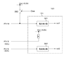
- FIG. 1 shows a configuration example of an AV (Audio and Visual) system 100 according to an embodiment.
- the AV system 100 is configured by connecting a source device and a sink device.
- the source device 110 is, for example, an AV source such as a game console, a disc player, a set top box, a digital camera, a mobile phone, and the like.
- the sink device 120 is, for example, a television receiver, a projector, or the like.
- the source device 110 and the sink device 120 are connected via a cable 200.
- the source device 110 is provided with a connector unit 111 to which the data transmission unit 112 is connected.
- the sink device 120 is provided with a connector unit 121 to which the data receiving unit 122 is connected.
- One end of the cable 200 is connected to the connector portion 111 of the source device 110, and the other end of the cable 200 is connected to the connector portion 121 of the sink device 120.
- the source device 110 includes a control unit 113.
- the control unit 113 controls the entire source device 110.
- the data transmission unit 112 of the source device 110 supports only the digital interface of the HDMI standard, it may support only the digital interface of the new standard, or may support both of them.
- the control unit 113 selectively switches the operation of one of the digital interfaces.
- the control unit 113 of the source device 110 includes a determination unit 114.
- the determination unit 114 determines, using a circuit, whether the sink device 120 is connected to the source device 110, and whether the digital interface of the data reception unit 122 of the sink device 120 is the HDMI standard or the new standard. .
- the control unit 113 supports the digital interface of the data reception unit 122 of the sink device 120 based on the determination result of the determination unit 114. The operation of the data transmission unit 112 is switched to perform the above operation.
- the sink device 120 includes a control unit 123.
- the control unit 123 controls the entire sink device 120.
- the data receiving unit 122 of the sink device 120 supports only the digital interface of the HDMI standard
- the data receiving unit 122 may support only the digital interface of the new standard, or may support both of them.
- the control unit 123 selectively switches the operation to one of the digital interfaces.
- the control unit 123 of the sink device 120 includes a determination unit 124.
- the determination unit 124 uses a circuit to determine whether the source device 110 is connected to the sink device 120, and whether the digital interface of the data transmission unit 112 of the source device 110 is the HDMI standard or the new standard. .
- the control unit 123 supports the digital interface of the data transmitting unit 112 of the source device 110 based on the determination result of the determining unit 124.
- the operation of the data receiving unit 122 is switched to perform the above operation.
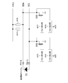
- FIG. 2 shows a configuration example of the data transmission unit 112 of the source device 110 and the data reception unit 122 of the sink device 120 in the AV system 100 of FIG.
- This configuration example shows the case where the digital interface of the data transmission unit 112 and the data reception unit 22 is a digital interface of the HDMI standard.
- the data transmission unit 112 transmits a differential signal corresponding to pixel data of an image of one non-compressed screen in an effective image period (hereinafter, appropriately referred to as an active video period) to a plurality of data reception units 122.
- the effective image interval is an interval from the interval from one vertical synchronization signal to the next vertical synchronization signal excluding the horizontal blanking interval and the vertical blanking interval.
- the data transmission unit 112 receives, in a plurality of channels, differential signals corresponding to at least audio data, control data, other auxiliary data, and the like attached to an image in a horizontal blanking interval or a vertical blanking interval. Transmit to section 122 in one direction.
- the transmission channels of the HDMI system including the data transmission unit 112 and the data reception unit 122 include the following transmission channels. That is, three TMDS channels # 0 to ## 3 as transmission channels for serially transmitting pixel data and audio data in one direction in synchronization with the pixel clock from data transmission unit 112 to data reception unit 122. There are two. There is also a TMDS clock channel as a transmission channel for transmitting a TMDS clock.
- the data transmission unit 112 has an HDMI transmitter 81.
- the HDMI transmitter 81 converts, for example, pixel data of an uncompressed image into a corresponding differential signal, and is connected via an HDMI cable with three TMDS channels # 0, # 1, and # 2 that are a plurality of channels. Serial transmission in one direction is performed to the data reception unit 122 which is
- the HDMI transmitter 81 converts audio data associated with the uncompressed image, necessary control data and other auxiliary data, etc. into corresponding differential signals, and converts the three TMDS channels # 0, # 1, # 1, and so on. Serial transmission is performed unidirectionally to the data receiving unit 122 in # 2.
- the HDMI transmitter 81 transmits TMDS clocks synchronized with pixel data transmitted by the three TMDS channels # 0, # 1, and # 2 to the data transmission unit 122 connected via the HDMI cable via the TMDS clock channel. Send.
- the data reception unit 122 receives a differential signal corresponding to pixel data transmitted in one direction from the data transmission unit 122 on a plurality of channels in an active video period. In addition, the data reception unit 122 transmits differential signals corresponding to audio data and control data, which are transmitted in one direction from the data transmission unit 112 on a plurality of channels in the horizontal blanking interval or the vertical blanking interval. To receive.
- the data receiving unit 122 has the HDMI receiver 82.
- the HDMI receiver 82 is a TMDS channel # 0, # 1, # 2 and a differential signal corresponding to pixel data transmitted in one direction from the data transmission unit 112 and a difference corresponding to audio data or control data. Receive dynamic signals. In this case, the signal is received in synchronization with the pixel clock (TMDS clock) transmitted from the data transmission unit 112 through the TMDS clock channel.
- TMDS clock pixel clock
- DDC Display Data Channel
- the DDC is composed of two signal lines (not shown) included in the HDMI cable.
- E-EDID Enhanced Extended Display Identification Data
- the data receiving unit 122 has an EDID ROM (Read Only Memory) that stores E-EDID which is performance information on its own performance (Configuration / capability).
- the data transmission unit 112 reads out the E-EDID from the data reception unit 122 connected via the HDMI cable via the DDC, for example, in response to a request from the control unit 113.
- the data transmission unit 112 transmits the read E-EDID to the control unit 113.
- the control unit 113 stores the E-EDID in a flash ROM or a DRAM (not shown).
- the control unit 113 can recognize the setting of the performance of the data receiving unit 122 based on the E-EDID. For example, the control unit 113 recognizes whether or not the sink device 120 having the data receiving unit 122 can handle stereoscopic image data, and if possible, can further correspond to any TMDS transmission data structure.
- the CEC line is formed of a single signal line (not shown) included in the HDMI cable, and is used to perform bidirectional communication of control data between the data transmission unit 112 and the data reception unit 122. This CEC line constitutes a control data line.
- the HDMI cable includes a line (HPD line) connected to a pin called HPD (Hot Plug Detect).
- HPD Hot Plug Detect
- the source device can detect the connection of the sink device using this HPD line.
- This HPD line is also used as a HEAC- line that constitutes a bi-directional communication path.
- the HDMI cable includes a power line (+5 V Power Line) used to supply power from the source device to the sink device.
- the HDMI cable includes a utility line. This utility line is also used as an HEAC + line that constitutes a bi-directional communication path.
- FIG. 3 shows an example of the structure of TMDS transmission data.
- FIG. 3 shows sections of various transmission data in the case where image data of 1920 pixels wide ⁇ 1080 lines wide is transmitted in the TMDS channels # 0, # 1, and # 2.
- Video Field Three types of sections exist in the video field (Video Field) in which the transmission data is transmitted by the three TMDS channels # 0, # 1, and # 2 of the HDMI, depending on the type of the transmission data. These three types of sections are a video data section (Video Data period), a data island section (Data Island period), and a control section (Control period).
- the video field interval is an interval from the rising edge (active edge) of a certain vertical synchronization signal to the rising edge of the next vertical synchronization signal.
- the video field period is divided into a horizontal blanking period, a vertical blanking period, and an active video period.
- This active video interval is an interval obtained by removing the horizontal blanking interval and the vertical blanking interval from the video field interval.
- Video data intervals are assigned to active video intervals.
- data of effective pixels (Active pixels) equivalent to 1920 pixels (pixels) ⁇ 1080 lines constituting image data of one non-compressed screen is transmitted.
- the data island period and the control period are assigned to the horizontal blanking period and the vertical blanking period.
- Auxiliary data (Auxiliary data) is transmitted in the data island period and the control period. That is, the data island period is allocated to a part of the horizontal blanking period and the vertical blanking period.
- the data island period for example, a packet of audio data, which is data not related to control, is transmitted.
- the control period is assigned to the horizontal blanking period and other parts of the vertical blanking period.
- data related to control for example, a vertical synchronization signal and a horizontal synchronization signal, a control packet, etc. are transmitted.
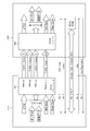
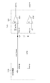
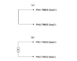
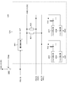
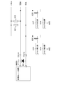
- FIG. 4 shows an example of the pin arrangement of the HDMI receptacle.
- the pin arrangement shown in FIG. 4 is called type A (type-A).
- the TMDS Data # i + and TMDS Data # i ⁇ which are differential signals of the TMDS channel #i are transmitted by two lines which are differential lines. These two lines are a pin to which TMDS Data # i + is assigned (pin with pin numbers 1, 4 and 7) and a pin to which TMDS Data # i- is assigned (pin number is 3, 6, Connected to pin 9).
- a CEC line through which a CEC signal which is control data is transmitted is connected to a pin having a pin number of 13.
- a line through which an SDA (Serial Data) signal such as E-EDID is transmitted is connected to a pin having a pin number of 16.
- a line through which an SCL (Serial Clock) signal, which is a clock signal used for synchronization at the time of transmission and reception of the SDA signal, is transmitted is connected to a pin having a pin number of 15.
- the above-mentioned DDC is composed of a line through which the SDA signal is transmitted and a line through which the SCL signal is transmitted.
- the HPD line (HEAC-line) for the source device to detect the connection of the sink device is connected to the pin having a pin number of 19.
- the utility line (HEAC + line) is connected to the pin whose pin number is 14.
- the power supply line for supplying power is connected to the pin having a pin number of 18.
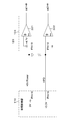
- FIG. 5 shows a configuration example of the data transmission unit 112 of the source device 110 and the data reception unit 122 of the sink device 120 in the AV system 100 of FIG.
- This configuration example shows the case where the digital interface of the data transmission unit 112 and the data reception unit 122 is a digital interface of the new standard.
- parts corresponding to FIG. 2 are given the same reference numerals, and the detailed description thereof will be omitted as appropriate.
- the data transmission unit 112 transmits a differential signal corresponding to pixel data of an image of one non-compressed screen in an effective image period (hereinafter, appropriately referred to as an active video period) to a plurality of data reception units 122.
- the effective image interval is an interval from the interval from one vertical synchronization signal to the next vertical synchronization signal excluding the horizontal blanking interval and the vertical blanking interval.
- the data transmission unit 112 transmits a differential signal corresponding to at least audio data, control data, other auxiliary data, and the like associated with an image in one TMDS channel # 0 in the horizontal blanking interval or the vertical blanking interval. , And transmit data to the data receiving unit 122 in one direction.
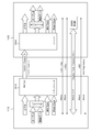
- the TMDS clock is tripled in the case of the HDMI standard (see FIG. 2) to enable transmission on only the TMDS channel # 0. Further, the TMDS clock itself is also inserted in the TMDS channel # 0 in the common mode, thereby eliminating the need for the TMDS clock channel. Therefore, in the digital interface of this new standard, among the pins of the HDMI receptacle (A type), nine in the case of the digital interface of the HDMI standard, TMDS channel # 1, TMDS channel # 2, and TMDS clock channel are used Pins (PIN1-6, 10-12) are unused.
- the data transmission unit 112 has a transmitter 81A.
- the transmitter 81A converts, for example, pixel data of an uncompressed image into a corresponding differential signal, and is connected to the data reception unit 122 connected via an HDMI cable or a new standard cable by one TMDS channel # 0. Serial transmission in one direction.
- the transmitter 81A converts audio data attached to the non-compressed image, necessary control data and other auxiliary data, etc. into corresponding differential signals, and one TMDS channel # 0 transmits the data receiver 122. Serial transmission in one direction.
- the data reception unit 122 receives a differential signal corresponding to pixel data, which is transmitted in one direction from the data transmission unit 122 on one channel # 0 in an active video period.
- the data reception unit 122 corresponds to audio data and control data transmitted in one direction from the data transmission unit 112 on a plurality of one channel # 0 in the horizontal blanking interval or the vertical blanking interval. Receive differential signals.
- the data receiving unit 122 has a receiver 82A.
- the receiver 82A receives a differential signal corresponding to pixel data and a differential signal corresponding to audio data or control data, which are transmitted in one direction from the data transmission unit 112 through the TMDS channel # 0.
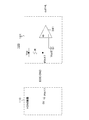
- FIG. 6 shows a configuration example of the data transmission unit 112 of the source device 110 and the data reception unit 122 of the sink device 120 in the AV system 100 of FIG.
- This configuration example also shows the case where the digital interface of the data transmission unit 112 and the data reception unit 122 is a digital interface of the new standard.
- parts corresponding to those in FIG. 5 are denoted by the same reference numerals, and the detailed description thereof will be omitted as appropriate.
- the data transmission unit 112 at least supports audio data and control data attached to the image in the horizontal blanking interval or the vertical blanking interval. Differential signals corresponding to data and the like are unidirectionally transmitted to the data receiving unit 122 on one TMDS channel # 0.
- the TMDS clock is tripled in the case of the HDMI standard (see FIG. 2) to enable transmission on only the TMDS channel # 0. Further, the TMDS clock itself is also inserted in the TMDS channel # 0 in the common mode, thereby eliminating the need for the TMDS clock channel. In this case, two pins PIN1 and PIN2 of the HDMI receptacle are used.
- one control line (Control Line) is used as a line of CEC, DDC, and HPD. Also, the power supply line (+5 V Power Line) is omitted. Also, like USB, a VBUS line (VBUS Line) is added for charging a portable source device, and a grand line (Grand Line) is commonly provided.
- VBUS Line VBUS Line
- Gram Line grand line
- the control line is connected to the pin whose pin number is three. Also, the VBUS line is connected to the pin whose pin number is four. Furthermore, the ground line is connected to the pin whose pin number is 5. Therefore, in the digital interface of the new standard shown in FIG. 6, among the pins of the HDMI receptacle (A type), the 14 pins of the PIN 6-19 are not used.
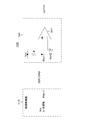
- the data receiving unit 122 of the sink device 120 is matched to the digital interface of the data transmitting unit 112 of the source device 110 if it can support both the HDMI standard and the new standard digital interface. It is controlled to perform an operation. That is, when the cable 200 is connected to the connector unit 121 after power on, the control unit 123 determines whether the digital interface of the data transmission unit 112 of the source device 110 is the HDMI standard or the new standard, and the determination result is In response, it controls the operation of the data receiving unit 122.
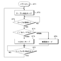
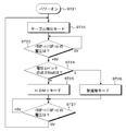
- the flowchart of FIG. 7 shows a control procedure of the control unit 123.
- the control unit 123 starts processing with power on, and then proceeds to processing of the cable detection mode in step ST2.
- the cable detection mode the connection of the cable 200 to the connector portion 121 is detected from the voltage at the 18th pin of the connector portion 121, the output of a sensor for detecting the cable connection, and the like.
- step ST3 the control unit 123 determines whether the cable 200 is connected to the connector unit 121 based on the detection result in step ST2.
- the control unit 123 proceeds to the process of step ST4.
- step ST4 the control unit 123 determines whether the digital interface of the data transmission unit 112 of the source device 110 is the HDMI standard or the new standard based on the determination result of the determination unit 124.
- step ST5 the control unit 123 controls the data receiving unit 122 to an operation mode (HDMI mode) in accordance with the digital interface of the HDMI standard.
- step ST6 the control unit 123 controls the data receiving unit 122 to an operation mode (new standard mode) in accordance with the digital interface of the new standard.
- control unit 123 determines whether or not cable 200 has been pulled out in step ST7, and maintains the operation mode of data reception unit 122 as it is unless the cable 200 is pulled out. .
- the process immediately returns to step ST2.
- the digital interface of the data reception unit 122 of the sink device 120 is used. It is controlled to perform the combined operation. That is, when the cable 200 is connected to the connector unit 111 after power on, the control unit 113 determines whether the digital interface of the data reception unit 122 of the sink device 120 is the HDMI standard or the new standard, and the determination result is In response, it controls the operation of the data transmission unit 112.
- the control procedure of the control unit 113 is the same as the control procedure of the control unit 123 of the above-described sink device 120 although the detailed description is omitted (see FIG. 7).
- This configuration example is an example in which determination is made only with the TMDS differential signal line. Among multiple TMDS differential signal pairs, only one is detected as an active signal pair. For example, as shown in the configuration example of FIG. 5, the HDMI standard uses three TMDS channels # 0 to # 2, but the new standard (see FIG. 5) uses only one TMDS channel # 0. . Therefore, in the new standard, TMDS channels # 1, # 2 and TMDS clock channel are not used.
- the data transmission unit 112 of the source device 110 when the data transmission unit 112 of the source device 110 operates with the digital interface of the HDMI standard, a differential signal is input, and the transmission unit 112 of the source device 110 is digital of the new standard (see FIG. 5).
- Active range detection circuits are provided for a pair of pins, for example, PIN 1 and PIN 3 to which differential signals are not input when operating at the interface. Based on the detection result of the active range detection circuit, it is possible to determine whether the digital interface of the data transmission unit 112 of the source device 110 is the HDMI standard or the new standard.
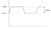
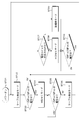
- FIG. 8 shows a schematic diagram of a TMDS differential signal pair.
- the TMDS differential signal operates within this range as the upper limit voltage V_high, the lower limit voltage V_low, and the amplitude Vswing, as shown in FIG.
- the active range detection circuit outputs "H” if any of the differential signal pairs is within the specified voltage range of TMDS, and one or both of the differential signal pairs are outside the specified voltage range of TMDS. If there is, it is a circuit that outputs "L".
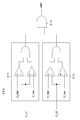
- FIG. 10 shows a specific circuit example of the active range detection circuit 310 for digital interface determination.
- This circuit example is configured by two window comparators 311 and 312 and one AND circuit 313.
- window comparators 311 and 312 connect the upper limit voltage of TMDS to V_high and the lower limit voltage to V_low and connect one differential signal pair to V_c
- the AND circuit output is within the specified range of V_high> V_c> V_low. It becomes "H”.
- the voltage V_c1 of PIN1 is input to the window comparator 311, and the voltage V_c3 of PIN3 is input to the window comparator 312.
- the outputs of the window comparators 311 and 312 are input to the AND circuit 313, and the output of the AND circuit 313 becomes the output outA of the active range detection circuit 310.
- the active range detection circuit is provided for a pair of pins, for example, the PINs 7 and 9 to which differential signals are input also in the case of. Based on the detection result of the active range detection circuit, it is possible to determine whether or not the source device 110 is connected via the cable 200.
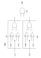
- FIG. 11 shows a specific circuit example of the active range detection circuit 320 for source device connection determination.
- This circuit example is configured by two window comparators 321 and 322 and one AND circuit 323.
- window comparators 321 and 322 set the upper limit voltage of TMDS to V_high and the lower limit voltage to V_low and connect one differential signal pair to V_c
- the AND circuit output is within the specified range of V_high> V_c> V_low. It becomes "H”.
- the voltage V_c7 of the PIN 7 is input to the window comparator 321, and the voltage V_c9 of the PIN 9 is input to the window comparator 322.
- the outputs of the window comparators 321 and 322 are input to the AND circuit 323, and the output of the AND circuit 323 becomes the output outB of the active range detection circuit 320.
- the active range detection circuits 310 and 320 provided in the determination unit 124 in the control unit 123 of the sink device 120 have been described. However, by providing the same active range detection circuit in the determination unit 114 in the control unit 113 of the source device 110, it is determined whether the sink device 120 is connected, and the digital interface of the data reception unit 122. It is possible to determine whether the is the HDMI standard or the new standard.
- the transmission unit 112 of the source device 110 uses the digital interface of the new standard (see FIG. 5).
- Active range detection circuits are provided for a pair of pins that do not output differential signals when operating, for example, PIN 1 and PIN 3. Based on the detection result of the active range detection circuit, it is possible to determine whether the digital interface of the data reception unit 122 of the sink device 120 is the HDMI standard or the new standard.
- an active range detection circuit is provided for a pair of pins that output differential signals, for example, the PINs 7 and 9. Based on the detection result of the active range detection circuit, it is possible to determine whether the sink device 120 is connected via the cable 200 or not.
- This configuration example is an example in which the determination is performed using a signal other than the TMDS differential signal line.
- the power supply line (+5 V Power Line) connected to pin 18 and the HPD line connected to pin 19 are not used. Therefore, in this example, this power supply line and the HPD line are used.
- the data transmission unit 112 of the source device 110 operates with the digital interface of the HDMI standard, +5 V power is supplied from the source device 110 to the sink device 120 via the power supply line as shown in FIG.
- the 18th pin of the connector section 121 to which the power supply line is connected and the 19th pin of the connector section 121 to which the HPD line is connected are connected via a diode and a resistor. Therefore, when the sink device 120 is connected to the source device 110, the voltage of the HPD line becomes high, so that the source device 110 can confirm that the sink device 120 is connected.
- the data transmission unit 112 of the source device 110 operates with the digital interface according to the new standard (see FIG. 6), as shown in FIG. It is set to a voltage below 7 V), for example 0V. Also, pin 19 is set to a voltage higher than the voltage applied to pin 18, for example, + 3.3V.
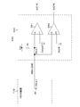
- the determining unit 124 in the control unit 123 of the sink device 120 is provided with two voltage comparators 331 and 332. +4.7 V is input to the positive input terminal of the voltage comparator 331, and the voltage at the 18th pin of the connector section 121 is input to the negative input terminal. The voltage at the 19th pin of the connector section 121 is input to the positive input terminal of the voltage comparator 332, and 0V is input to the negative input terminal.
- the outputs out1 and out2 of the voltage comparators 331 and 332 make it possible to determine whether the digital interface of the data transmission unit 112 is the HDMI standard or the new standard. If the cable is not connected, it can not be set to the HPD line +3.3 V, so the cable connection judgment is unnecessary.
- the diode and the resistor are required in the case of the HDMI standard device, but in the case of the new standard connection, the diode is not biased since it is reverse biased, and there is no problem in the operation.
- This configuration example is also an example in which determination is made by using signals other than the TMDS differential signal line.
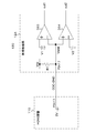
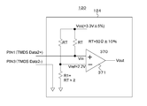
- the DDC-GND line connected to the 17th pin is not used. Therefore, in this example, this DDC-GND line is used.
- the 17th pin to which the DDC-GND line is connected is grounded.
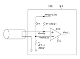
- Vcc for example, +5 V
- the 17th pin of the connector section 121 is pulled up to Vcc via the resistor R.
- the determination unit 124 in the control unit 123 of the sink device 120 is provided with one voltage comparator 341.
- the voltage at the 17th pin of the connector unit 121 is input to the positive input terminal of the voltage comparator 341.
- Vcc / 2 is input to the negative input terminal of the voltage comparator 341.
- the output out1 of the voltage comparator 341 makes it possible to determine whether the digital interface of the data transmission unit 112 is the HDMI standard or the new standard. In this configuration example, it is not possible to distinguish between the case where the digital interface of the data transmission unit 112 of the source device 110 is a new standard and the case where it is not connected, so cable connection determination is required separately.
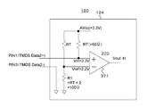
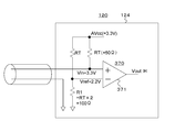
- This configuration example is also an example in which determination is made by using signals other than the TMDS differential signal line.
- the DDC-GND line connected to the 17th pin is not used. Therefore, in this example, this DDC-GND line is used.
- the 17th pin to which the DDC-GND line is connected is grounded.
- the 17th pin is grounded via the resistor R2.
- 3Vcc / 4 is input to the negative input terminal of the voltage comparator 351.
- the voltage comparator 351 compares the voltage at pin 17 with the upper voltage of the voltage obtained by dividing Vcc by the resistors R1 and R2.
- Vcc / 4 is input to the negative input terminal of the voltage comparator 352.
- the voltage comparator 352 compares the voltage at pin 17 with the lower voltage obtained by dividing Vcc by the resistors R1 and R2.
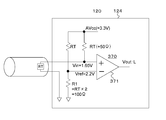
- This configuration example is also an example in which determination is made by using signals other than the TMDS differential signal line.
- the DDC-GND line connected to the 17th pin is not used. Therefore, in this example, this DDC-GND line is used.
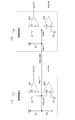
- the source device 110 is an HDMI device, as shown in FIG. 18, in the source device 110, the 17th pin to which the DDC-GND line is connected is grounded.
- the voltage obtained by dividing Vcc (for example, +5 V) by the resistors R1 and R2 is obtained at pin 17 Applied.
- the determination unit 114 in the control unit 113 is provided with two voltage comparators 361 and 362.
- the voltage at the 17th pin of the connector section 111 is input to the negative input terminal of the voltage comparator 361 and the positive input terminal of the voltage comparator 362.
- the voltage V3 is input to the positive input terminal of the voltage comparator 361.
- the voltage V4 is input to the negative input terminal of the voltage comparator 362.
- the sink device 120 When the sink device 120 is an HDMI device, as shown in FIG. 20, in the sink device 120, the 17th pin to which the DDC-GND line is connected is grounded. Further, when the sink device 120 is a new standard device (see FIG. 6), as shown in FIG. 19, the 17th pin is pulled up to the voltage Vcc via the resistor R1. Further, the determination unit 124 in the control unit 123 is provided with two voltage comparators 363 and 364. The voltage at the 17th pin of the connector unit 111 is input to the negative input terminal of the voltage comparator 363 and the positive input terminal of the voltage comparator 364. The voltage V1 is input to the positive input terminal of the voltage comparator 363. The voltage V2 is input to the negative input terminal of the voltage comparator 364.
- each connection state can be detected by the combination of the outputs out1 and out2 and out3 and out4 of the voltage comparator.
- the outputs of all of out1 to out4 become "H".
- V1 3/4 * Vcc
- V2 1/4 * Vcc
- V3 5/12 * Vcc
- V4 1/4 * Vcc
- the voltage comparator 363 of the sink device 120 compares the voltage at pin 17 with the upper voltage of the voltage obtained by dividing Vcc by the parallel resistor of resistors R1 and R1 and resistor R2. Ru.
- the voltage comparator 364 of the sink device 120 compares the voltage at pin 17 with the lower voltage obtained by dividing Vcc by the parallel resistance of the resistors R1 and R1 and the resistor R2.
- This configuration example is an example in which determination is made only with the TMDS differential signal line.
- a differential signal is input, and the transmission unit 112 of the source device 110 is digital of the new standard (see FIG. 5). Focus on a pair of pins to which no differential signal is input, for example, PIN 1 and PIN 3 when operating at the interface.
- the impedance between PIN1 and PIN3 on the sink device side is as follows. (1) When no HDMI cable is inserted: High impedance (2) When only HDMI cable is inserted: High impedance (3) When HDMI cable + HDMI source device is connected: High impedance
- the PIN1 and PIN3 are not connected, and thus become high impedance. Also, even when an HDMI source device is connected, it is in high impedance to protect the device.
- FIG. 22 illustrates the cable detection circuit 370 provided in the determination unit 124 in the control unit 123 of the sink device 120.
- FIG. 23 is a circuit example in the case where the cable detection circuit 370 of FIG. 22 is inserted into the TMDS differential pair schematic diagram shown in FIG.
- the switch D1 when cable detection is performed, the switch D1 is ON, the switch D2 is OFF, the switch D3 is ON, and the switch D4 is ON. Conversely, when the switch D1: OFF, the switch D2: ON, the switch D3: OFF, and the switch D4: OFF, the circuit returns to the equivalent circuit of FIG.
- the “cable detection mode” refers to a state immediately after the new device 120 is powered on.
- the cable detection circuit 370 shown in FIG. 22 is effective only in this mode. Also, all signal lines not related to the cable detection circuit 370 should be high impedance so as not to damage the source device unexpectedly.
- the “HDMI mode” is a signal configuration shown in FIG. 2 and a state where the sink device satisfies the requirements of the sink device defined by HDMI Ver 1.4.
- the “new standard mode” is a signal configuration shown in FIGS. 5 and 6 as an example, and the state where the sink device satisfies the requirements of the sink device defined in the new standard.
- the flowchart in FIG. 30 shows the control procedure of the control unit 123 of the sink device 120 when this detection method is used.
- the control unit 123 starts processing with power on, and then shifts to the cable detection mode in step ST12.
- the control unit 123 determines whether or not the cable sensor (see FIG. 29) has detected insertion of a cable.
- the control unit 123 proceeds to the process of step ST14.
- the control unit 123 determines whether the output Vout of the voltage comparator 371 of the cable detection circuit 370 (see FIG. 22) is "H" or "L".
- step ST15 the control unit 123 controls the data receiving unit 122 to an operation mode (HDMI mode) in accordance with the digital interface of the HDMI standard.
- step ST16 the control unit 123 controls the data receiving unit 122 to the operation mode (new standard mode) in accordance with the digital interface of the new standard.
- step ST7 the control unit 123 determines in step ST7 whether or not the cable has been pulled out, and maintains the operation mode of the data receiving unit 122 as it is unless the cable is pulled out. On the other hand, if data has been extracted, the process immediately returns to step ST12.
- the flowchart in FIG. 31 illustrates the control procedure of the control unit 123 of the sink device 120 when this detection method is used.
- the control unit 123 starts processing with power on, and then shifts to the cable detection mode in step ST22.
- the control unit 123 determines whether or not the voltage of the +5 V pin (18 pin) is +5 V.
- the control unit 123 proceeds to the process of step ST24.
- the control unit 123 determines whether the output Vout of the voltage comparator 371 of the cable detection circuit 370 (see FIG. 22) is "H" or "L".
- step ST ⁇ b> 25 the control unit 123 controls the data receiving unit 122 to an operation mode (HDMI mode) in accordance with the digital interface of the HDMI standard.
- step ST26 the control unit 123 controls the data receiving unit 122 to an operation mode (new standard mode) in accordance with the digital interface of the new standard.
- step ST27 the control unit 123 determines whether or not the cable has been pulled out. That is, when the voltage of the +5 V pin (18 pin) is 0 V, it is determined that there is a pullout. As long as the cable is not pulled out, the operation mode of the data receiving unit 122 is maintained as it is. On the other hand, when data is extracted, the control unit 123 immediately returns to step ST22.
- the flowchart in FIG. 32 also shows a control procedure of the control unit 123 of the sink device 120 in the case of using a method of monitoring and detecting the voltage of the +5 V pin (18 pin). However, this is the process when the new standard does not use the + 5V pin.
- the control procedure of the flow chart of FIG. 31 described above is different from that of the flow chart of FIG.
- the voltage comparator output Vout is seen, and transition is made to the HDMI mode or the new standard mode.
- step ST31 the control unit 123 starts processing with power on, and then shifts to the cable detection mode in step ST32. Then, in step ST33, the control unit 123 determines whether or not the voltage of the + 5V pin (18th pin) is + 5V. When the voltage of the +5 V pin (18 pin) is +5 V, in step ST34, the control unit 123 controls the data receiving unit 122 to an operation mode (HDMI mode) in accordance with the digital interface of the HDMI standard.
- HDMI mode HDMI mode
- step ST35 the control unit 123 determines the voltage of the +5 V pin (18 pin).
- the control unit 123 maintains the operation mode (HDMI mode) of the data reception unit 122 as it is.
- the control unit 123 immediately shifts to the cable detection mode in step ST36, and then shifts to the process in step ST37.
- step ST33 when the voltage of the + 5V pin (pin 18) is 0 V, the control unit 123 proceeds to the process of step ST37.
- step ST37 the control unit 123 determines whether the output Vout of the voltage comparator 371 of the cable detection circuit 370 (see FIG. 22) is "H” or "L".
- step ST ⁇ b> 38 the control unit 123 controls the data receiving unit 122 to an operation mode (HDMI mode) in accordance with the digital interface of the HDMI standard.
- step ST39 the control unit 123 controls the data receiving unit 122 to an operation mode (new standard mode) in accordance with the digital interface of the new standard.
- step ST40 determines the voltage of the +5 V pin (18 pin) in step ST40.
- the control unit 123 maintains the operation mode (HDMI mode or new standard mode) of the data reception unit 122 as it is.
- the control unit 123 immediately returns to step ST32.
- FIG. 33 shows a cable line layout based on the new standard.
- FIG. 34 shows a cable line layout of a new standard cable. Inside the HDMI Type-A plug on the sink device side of the new standard cable, the PIN 15 (15 pin) and the PIN 16 (16 pin) are shorted with a conducting wire, or the PIN 15 and PIN 16 are connected with a resistor R.
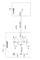
- FIG. 35 shows a schematic configuration of the determination unit 124 in the control unit 123 of the sink device 120.
- the determination unit 124 includes a voltage detector 381.
- the PIN 18 pin 18
- the PIN 18 is a power supply pin to which a power supply line (+5 V Power Line) is connected when an HDMI source device is connected.
- the voltage detector 381 detects the voltage state of the PIN 18. That is, the voltage detector 381 detects whether the voltage state of the PIN 18 is the voltage of the power supply and outputs the detection result out1.
- the determination unit 124 pulls up the PIN 15 (pin 15) to the power supply voltage Vcc via the resistor R.
- the determination unit 124 also includes a current detector 382.
- the PIN 16 (16th pin) is connected to the input side of the current detector 382.
- the current detector 382 detects the current state of the PIN 16. That is, the current detector 382 detects whether current flows through the PIN 16 and outputs the detection result out2.
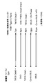
- the detection operation of the voltage detector 381 and the current detector 382 in the determination unit 124 described above will be considered in the following six cases. (1) When cable is not connected (2) When HDMI cable is connected (3) When HDMI cable + HDMI source device (power off) is connected (4) HDMI cable + HDMI source device (power on) is connected (5) When a new standard cable is connected (6) When a new standard cable + new standard source device (both power on / off) is connected
- the voltage detector 381 detects that the voltage state of the PIN 18 is not the voltage of the power supply. In addition, since there is a high impedance state between the PIN 15 and the PIN 16, no current flows through the PIN 16, and the current detector 382 detects that no current flows.
- the voltage detector 381 detects that the voltage state of the PIN 18 is not the voltage of the power supply. Also, the SCL line and the SDA line in the HDMI cable are not connected. Therefore, in this case as well, the PIN 15 and the PIN 16 are in a high impedance state. Therefore, no current flows through the PIN 16, and the current detector 382 detects that no current flows.
- the voltage detector 381 detects that the voltage state of the PIN 18 is not the voltage of the power supply.
- the PIN 15 and the PIN 16 are short-circuited with a conducting wire, or connected via a resistor R. Therefore, current flows through the PIN 16, and the current detector 382 detects that current is flowing.
- cable detection is performed by the voltage detector 381 and the current detector 382.
- the flowchart in FIG. 36 shows the control procedure of the control unit 123 of the sink device 120 when this detection method is used.
- step ST51 the control unit 123 starts processing with power on, and then shifts to the cable detection mode in step ST52.
- the control unit 123 polls detection results of the voltage detector 381 and the current detector 382.
- step ST53 the control unit 123 determines whether or not the power supply voltage is detected by the voltage detector 381, that is, whether or not the voltage of the + 5V pin (pin 18) is + 5V (power supply voltage). Determine.
- the control unit 123 When the power supply voltage is detected, the control unit 123 corresponds to “(4) HDMI cable + HDMI source device (power on) connected” described above, and in step ST54 the data reception unit 122 Control to the operation mode (HDMI mode) according to the digital interface of the HDMI standard. Then, in step ST55, the control unit 123 monitors the voltage detection state of the voltage detector 381 and maintains the operation mode (HDMI mode) of the data reception unit 122 while detecting the power supply voltage. On the other hand, when the power supply voltage is not detected by the voltage detector 381, the control unit 123 immediately returns to the cable detection mode of step ST52.
- step ST56 When the power supply voltage is not detected by the voltage detector 381 in step ST53, it is determined in step ST56 whether or not the current is detected by the current detector 382. When the current is not detected, the control unit 123 “(1) When the cable is not connected, (2) When the HDMI cable is connected, (3) HDMI cable + HDMI source device (power off) is connected The polling process of steps ST53 and ST56 is repeated, as it corresponds to "when it is performed.”
- control unit 123 determines that the above-mentioned “(5) new standard cable is connected, (6) new standard cable + new standard source device ( In the step ST57, the control unit 123 controls the data receiving unit 122 to an operation mode (new standard mode) in conformity with the digital interface of the new standard, assuming that “when power on / off is connected”. .
- step ST58 the control unit 123 monitors the current detection state of the current detector 382, and maintains the operation mode (new standard mode) of the data reception unit 122 while detecting the current. On the other hand, when the current detector 382 detects no current, the control unit 123 immediately returns to the cable detection mode of step ST52.
- the control unit 123 when controlling the data receiving unit 122 to the new standard mode in step ST57, the control unit 123 supplies the switch control signal Csw to the connection switch 383 shown in FIG. 35 to turn it on.
- the power supply Vcc can be supplied to the source device side.
- the source device whose digital interface is a digital interface according to the new standard is a battery-powered electronic device and the battery is completely raised, the source device It can be determined that the digital interface is a new standard digital interface. Therefore, the data receiving unit 122 described above can be controlled to the new standard mode, and power can be supplied to the source device for charging.
- the transmission unit 112 of the source device 110 is a new standard (see FIG. 5)
- PIN 15 pin for SCL
- PIN 16 pin for SDA
- a configuration including the current detector 382 that detects the current state of the PIN 16 is shown.
- a configuration may be considered in which not the current state of the PIN 16 but the voltage state is detected.
- This configuration example also focuses on a pair of pins, for example, the PIN 15 (a pin for SCL) and the PIN 16 (a pin for SDA) as in the seventh configuration example described above.
- This pair of pins is used when the data transmission unit 112 of the source device 110 operates with the digital interface of the HDMI standard, and the transmission unit 112 of the source device 110 is the digital interface of the new standard (see FIG. 5) Not used if it works.
- FIG. 37 shows a cable line layout of a new standard cable.
- the PIN 16 (16 pin) and the PIN 15 (15 pin) are connected through the diode D1.
- the anode of the diode D1 is connected to the PIN 15
- the cathode is connected to the PIN 16 so that a signal (current) flows in one direction from the PIN 15 to the PIN 16.
- the diode D1 instead of the diode D1, another electronic element having the same function may be used.
- FIG. 38 shows a schematic configuration of the determination unit 124 in the control unit 123 in the sink device 120.
- the determination unit 124 includes a voltage detector 381.
- the PIN 18 pin 18
- the PIN 18 is a power supply pin to which a power supply line (+5 V Power Line) is connected when an HDMI source device is connected.
- the voltage detector 381 detects the voltage state of the PIN 18. That is, the voltage detector 381 detects whether the voltage state of the PIN 18 is the voltage of the power supply and outputs the detection result out1.
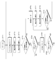
- the determination unit 124 includes a resistor (resistance element) 401, a field effect transistor 402, a pulse generator 403, a pulse detector 404, a resistance (resistance element) 405, a field effect transistor 406, and a pulse generator. And pulse detector 408.
- the resistor 401 constitutes a first resistance element
- the resistance element 405 constitutes a second resistance element
- the field effect transistor 402 constitutes a first switching element
- the field effect transistor 406 constitutes a second switching element.
- the resistance element 401, the field effect transistor 402, and the pulse generator 403 constitute a first signal supply unit. Further, the resistance element 405, the field effect transistor 406 and the pulse generator 407 constitute a second signal supply unit.
- the pulse detector 408 constitutes a first signal detector, and the pulse detector 404 constitutes a second signal detector.
- the resistance element 401 connects the PIN 15 (pin 15) to a power supply terminal to which a predetermined voltage, here, the power supply voltage + Vdd is supplied. That is, the resistive element 401 pulls up the PIN 15 to the power supply voltage + Vdd. Also, the drain of the field effect transistor 402 is connected to the PIN 15, and the source is grounded.
- the pulse generator 403 generates a pulse signal for driving a field effect transistor 402 as a switching element. That is, the pulse signal generated by the pulse generator 403 is supplied to the gate of the field effect transistor 402.
- the field effect transistor 402 is alternately turned on (conductive) and off (not conductive) based on the pulse signal from the pulse generator 403. That is, in the high level period of the pulse signal, the field effect transistor 402 is turned on (conductive), and the potential of the PIN 15 becomes the ground potential (0 V). On the other hand, in the low level period of the pulse signal, the field effect transistor 402 is turned off (non-passing), and the potential of the PIN 15 becomes the power supply voltage + Vdd.
- a pulse signal is supplied from the pulse generator 403 to the field effect transistor 402
- a pulse signal whose high level H is “+ Vdd” and whose low level L is “0 V” is supplied to the PIN 15 .
- the resistance element 405 connects the PIN 16 (16th pin) to a power supply terminal to which a predetermined voltage, here, the power supply voltage + Vdd is supplied. That is, the resistance element 405 pulls up the PIN 16 to the power supply voltage + Vdd. Also, the drain of the field effect transistor 406 is connected to the PIN 16 and the source is grounded.
- the pulse generator 407 generates a pulse signal for driving a field effect transistor 406 as a switching element. That is, the pulse signal generated by the pulse generator 407 is supplied to the gate of the field effect transistor 406.
- the field effect transistor 406 is alternately turned on (conducting) and off (not conducting) based on the pulse signal from the pulse generator 407. That is, in the high level period of the pulse signal, the field effect transistor 406 is turned on (conductive), and the potential of the PIN 16 becomes the ground potential (0 V). On the other hand, in the low level period of the pulse signal, the field effect transistor 406 is turned off (non-passing), and the potential of the PIN 16 becomes the power supply voltage + Vdd. Thus, when a pulse signal is supplied from the pulse generator 407 to the field effect transistor 406, a pulse signal whose high level H is “+ Vdd” and whose low level L is “0 V” is supplied to the PIN 16 .
- the pulse detector 404 detects the signal obtained at the PIN 15 during the period when the pulse signal whose high level H is “+ Vdd” and the low level L is “0 V” is supplied to the PIN 16 as described above.
- the detection result out2 is output.
- the pulse detector 408 detects a signal obtained in the PIN 16 during a period in which the pulse signal whose high level H is “+ Vdd” and the low level L is “0 V” is supplied to the PIN 15. , Output the detection result out3.
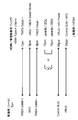
- the determination unit 124 extracts the case where the new standard cable is connected, based on the combination of the detection result out2 and the detection result out3 obtained in the following detection procedures A and B. First, detection procedures A and B will be described.
- a pulse signal is supplied from the pulse generator 403 to the gate of the field effect transistor 402, and a pulse signal whose high level H is “+ Vdd” and whose low level L is “0 V” is supplied to the PIN 15.
- the pulse detector 408 detects a signal obtained on the PIN 16, and outputs a detection result out3.
- the detection result out3 output from the pulse detector 408 is as follows.
- the pulse detector 408 outputs "N (No)" as the detection result out3 when no pulse signal is detected at all, that is, when the voltage of the PIN 16 remains unchanged at the power supply voltage + Vdd.
- the pulse detector 408 detects a complete pulse signal, that is, detects a pulse signal whose high level H is “+ Vdd” and whose low level L is “0 V”, “Y” is detected as the detection result out 3. (Yes) is output.
- the pulse detector 408 outputs “M (Medium)” as the detection result out3 when detecting an incomplete pulse signal, that is, when detecting a pulse signal whose low level L is 0 V ⁇ L ⁇ + Vdd. Do.
- Detection procedure B A pulse signal is supplied from the pulse generator 407 to the gate of the field effect transistor 406, and a pulse signal whose high level H is "+ Vdd” and whose low level L is “0 V” is supplied to the PIN 16.
- the pulse detector 404 detects a signal obtained on the PIN 15, and outputs a detection result out2.
- the detection result out2 output from the pulse detector 404 is as follows.
- the pulse detector 404 outputs "N (No)" as the detection result out2 when no pulse signal is detected at all, that is, when the voltage of the PIN 15 remains unchanged at the power supply voltage + Vdd.
- the pulse detector 404 detects a complete pulse signal, that is, detects a pulse signal whose high level H is “+ Vdd” and whose low level L is “0 V”, “Y” is detected as the detection result out 2. (Yes) is output.
- the pulse detector 404 outputs “M (Medium)” as the detection result out2 when detecting an incomplete pulse signal, that is, when detecting a pulse signal whose low level L is 0 V ⁇ L ⁇ + Vdd. Do.
- the pulse detector 408 detects a complete pulse signal, and outputs “Y (Yes)” as the detection result out3.
- the pulse detector 404 outputs "N (No)" as the detection result out2.
- FIG. 43 shows the connection state in this case.
- the impedance between the PIN 15 (SCL) and the PIN 16 (SDA) is any one of the following (5-1) to (5-3) depending on the state on the HDMI source device side.
- (5-1) high impedance
- 5-2) low impedance
- (5-3) intermediate between high impedance and low impedance
- the pulse detector 408 when the detection procedure A is executed, the pulse detector 408 outputs “Y (Yes)” as the detection result out3.
- the pulse detector 404 outputs “Y (Yes)” as the detection result out2.
- the pulse detector 408 when the detection procedure A is executed, the pulse detector 408 outputs “M (Medium)” as the detection result out3.
- the pulse detector 404 outputs “M (Medium)” as the detection result out2.
- FIG. 44 shows the detection procedure A in each of the above-mentioned cases (1) to (5) and the detection results out3 and out2 in the detection procedure B collectively.
- the detection result out3 of detection procedure A and detection The detection result out2 of step B is opposite.
- the impedance has extreme anisotropy (a low impedance in the SCL ⁇ SDA direction and a high impedance in the SDA ⁇ SCL direction).
- the detection result out3 of the detection procedure A matches the detection result out2 of the detection procedure B.
- step ST71 the control unit 123 starts processing with power on, and then shifts to the cable detection mode in step ST72.
- This cable detection mode is a mode in which the cable detection circuit shown in FIG. 38 is enabled and the other pins are disabled.
- step ST73 the control unit 123 executes the detection procedure A, and acquires the detection result out3 output from the pulse detector 408.
- step ST74 the control unit 123 executes the detection procedure B, and acquires the detection result out2 output from the pulse detector 404.
- step ST75 the control unit 123 determines whether the condition “detection result out3 of detection procedure A is“ Y (Yes) ”and the detection result out2 of detection procedure B is“ N (No) ””. To judge. When this condition is satisfied, the control unit 123 proceeds to the process of step ST76. In step ST76, the control unit 123 controls the data receiving unit 122 to an operation mode (new standard mode) in accordance with the digital interface of the new standard.
- step ST77 the control unit 123 executes the detection procedure A, and acquires the detection result out3 output from the pulse detector 408.
- step ST78 the control unit 123 executes the detection procedure B, and acquires the detection result out2 output from the pulse detector 404.
- step ST79 the control unit 123 determines whether the condition “detection result out3 of the detection procedure A is“ Y (Yes) ”and the detection result out2 of the detection procedure B is“ N (No) ”is satisfied. To judge.
- control unit 123 When the condition is satisfied, the control unit 123 maintains the operation mode (new standard mode) of the data reception unit 122 as it is. On the other hand, when this condition is not satisfied, the control unit 123 determines that the new standard cable has been disconnected, and returns to the cable detection mode of step ST72.
- step ST80 the control unit 123 determines whether or not the voltage detector 381 detects a power supply voltage, that is, whether the voltage of the + 5V pin (pin 18) is + 5V (power supply voltage). Do. When the power supply voltage is not detected by the voltage detector 381, the control unit 123 returns to step ST73 and repeats the processing of the detection procedure A and the detection procedure B.
- step ST81 the control unit 123 controls the data receiving unit 122 to an operation mode (HDMI mode) in accordance with the digital interface of the HDMI standard. Then, in step ST82, the control unit 123 monitors the voltage detection state of the voltage detector 381 and maintains the operation mode (HDMI mode) of the data reception unit 122 while detecting the power supply voltage.
- the HDMI mode the SDA line and the SCL line are used for the original application of HDMI such as EDID reading and HDCP authentication, so the detection procedures A and B are not performed.
- the control unit 123 immediately returns to the cable detection mode of step ST72.
- the control unit 123 When controlling the data reception unit 122 to the new standard mode in step ST76, the control unit 123 supplies the switch control signal Csw to the connection switch 383 shown in FIG. 38 to turn it on. Thus, the power supply Vcc can be supplied to the source device side.
- the data receiving unit 122 described above can be controlled to the new standard mode, and power can be supplied to the source device for charging.
- the transmission unit 112 of the source device 110 is the new standard (see FIG. 5)
- PIN 15 pin for SCL
- PIN 16 pin for SDA
- the field effect transistor 402 is driven by a pulse signal in the detection procedure A
- the field effect transistor 406 is driven by a pulse signal in the detection procedure B.
- the field effect transistors 402 and 406 are changed from the off state to the on state, and the pulse detectors 408 and 404 detect the change in voltage level, and the detection results out3 and out2 A configuration for acquiring In this case, the pulse generators 403 and 407 become unnecessary.
- the present invention can be applied to, for example, an AV system in which a source device and a sink device are connected via a digital interface.
- AV system 110 source device 111: connector unit 112: data transmission unit 113: control unit 114: discrimination unit 120: sink device 121: connector unit 122 ... Data reception unit 123 ... Control unit 124 ... Discrimination unit 200 ... Cable 310, 320 ... Active range detection circuit 331, 332, 341, 351, 352, 361-364 ... Voltage Comparator 370: Cable detection circuit 371: Voltage comparator 381: Voltage detector 382: Current detector 383: Connection switch 401, 405: Resistance (resistance element) 402, 406 ⁇ ⁇ ⁇ Field-effect transistor 403, 407 ⁇ ⁇ ⁇ Pulse generator 404, 408 ⁇ ⁇ ⁇ Pulse detector
Landscapes
- Engineering & Computer Science (AREA)
- Multimedia (AREA)
- Signal Processing (AREA)
- Computer Networks & Wireless Communication (AREA)
- General Physics & Mathematics (AREA)
- Computer Hardware Design (AREA)
- Physics & Mathematics (AREA)
- Theoretical Computer Science (AREA)
- Automation & Control Theory (AREA)
- Databases & Information Systems (AREA)
- Two-Way Televisions, Distribution Of Moving Picture Or The Like (AREA)
- Power Sources (AREA)
- Details Of Connecting Devices For Male And Female Coupling (AREA)
- Controls And Circuits For Display Device (AREA)
- Information Transfer Systems (AREA)
Priority Applications (6)
| Application Number | Priority Date | Filing Date | Title |
|---|---|---|---|
| RU2011140337/07A RU2553980C2 (ru) | 2010-02-12 | 2011-02-02 | Электронное устройство и способ определения цифрового интерфейса для подключенного внешнего устройства |
| EP11742152.9A EP2405654B1 (en) | 2010-02-12 | 2011-02-02 | Electronic apparatus and method to detect various connected HDMI interfaces |
| BRPI1106073A BRPI1106073A2 (pt) | 2010-02-12 | 2011-02-02 | dispositivo eletrônico, e, método de determinação de interface digital. |
| US13/262,730 US8862791B2 (en) | 2010-02-12 | 2011-02-02 | Electronic device and digital interface determining method of connected external device |
| KR1020117022982A KR101661787B1 (ko) | 2010-02-12 | 2011-02-02 | 전자 기기 및 접속 외부 기기의 디지털 인터페이스 판별 방법 |
| CN201180002038.7A CN102422638B (zh) | 2010-02-12 | 2011-02-02 | 电子设备和所连接的外部设备的数字接口确定方法 |
Applications Claiming Priority (6)
| Application Number | Priority Date | Filing Date | Title |
|---|---|---|---|
| JP2010-029545 | 2010-02-12 | ||
| JP2010029545 | 2010-02-12 | ||
| JP2010044778 | 2010-03-01 | ||
| JP2010-044778 | 2010-03-01 | ||
| JP2010067089A JP5515919B2 (ja) | 2010-02-12 | 2010-03-23 | 電子機器および接続外部機器のデジタルインタフェース判別方法 |
| JP2010-067089 | 2010-03-23 |
Publications (1)
| Publication Number | Publication Date |
|---|---|
| WO2011099407A1 true WO2011099407A1 (ja) | 2011-08-18 |
Family
ID=44367683
Family Applications (1)
| Application Number | Title | Priority Date | Filing Date |
|---|---|---|---|
| PCT/JP2011/052180 Ceased WO2011099407A1 (ja) | 2010-02-12 | 2011-02-02 | 電子機器および接続外部機器のデジタルインタフェース判別方法 |
Country Status (9)
| Country | Link |
|---|---|
| US (1) | US8862791B2 (enExample) |
| EP (1) | EP2405654B1 (enExample) |
| JP (1) | JP5515919B2 (enExample) |
| KR (1) | KR101661787B1 (enExample) |
| CN (1) | CN102422638B (enExample) |
| BR (1) | BRPI1106073A2 (enExample) |
| RU (1) | RU2553980C2 (enExample) |
| TW (1) | TWI539370B (enExample) |
| WO (1) | WO2011099407A1 (enExample) |
Cited By (3)
| Publication number | Priority date | Publication date | Assignee | Title |
|---|---|---|---|---|
| CN103733611A (zh) * | 2011-08-23 | 2014-04-16 | 索尼公司 | 信号转换装置、信号转换方法和终端装置 |
| US10327049B2 (en) | 2017-05-11 | 2019-06-18 | Kabushiki Kaisha Toshiba | Cable and electronic apparatus |
| CN113223441A (zh) * | 2021-05-20 | 2021-08-06 | 青岛中科英泰商用系统股份有限公司 | 一种显示扩展连接方法及装置 |
Families Citing this family (42)
| Publication number | Priority date | Publication date | Assignee | Title |
|---|---|---|---|---|
| KR101566174B1 (ko) | 2011-03-02 | 2015-11-05 | 삼성전자 주식회사 | 영상처리장치 및 그 제어방법 |
| US8855194B2 (en) * | 2011-05-09 | 2014-10-07 | Texas Instruments Incorporated | Updating non-shadow registers in video encoder |
| JP5444310B2 (ja) * | 2011-11-17 | 2014-03-19 | 株式会社東芝 | 双方向通信インタフェース装置、送信装置及び受信装置 |
| US8713316B2 (en) | 2011-12-13 | 2014-04-29 | Crestron Electronics Inc. | System, apparatus and method for enabling/disabling display data channel access to enable/disable high-bandwidth digital content protection |
| US8681977B2 (en) * | 2011-12-13 | 2014-03-25 | Crestron Electronics Inc. | Enabling/disabling display data channel access to enable/ disable high-bandwidth digital content protection |
| JP5571243B2 (ja) * | 2011-12-27 | 2014-08-13 | パナソニック株式会社 | 通信ケーブル |
| JP5994275B2 (ja) * | 2012-02-14 | 2016-09-21 | セイコーエプソン株式会社 | 表示装置、及び、表示装置の制御方法 |
| JP5870733B2 (ja) * | 2012-02-14 | 2016-03-01 | セイコーエプソン株式会社 | 表示装置、及び、表示装置の制御方法 |
| CN103259999B (zh) * | 2012-02-20 | 2016-06-15 | 联发科技(新加坡)私人有限公司 | Hpd信号输出控制方法、hdmi接收端设备及系统 |
| CN102779212A (zh) * | 2012-06-29 | 2012-11-14 | 浪潮电子信息产业股份有限公司 | 一种精确计算风扇板连接器Pin针数的方法 |
| US9788082B2 (en) * | 2012-09-04 | 2017-10-10 | Panasonic Intellectual Property Management Co., Ltd. | Terminal device and control method |
| TW201414103A (zh) * | 2012-09-28 | 2014-04-01 | Accton Technology Corp | 高速傳輸介面電路及其設計方法 |
| JP2014090280A (ja) * | 2012-10-30 | 2014-05-15 | Funai Electric Co Ltd | 映像音声信号処理装置 |
| TWI456397B (zh) * | 2012-11-26 | 2014-10-11 | Quanta Comp Inc | 電腦系統 |
| CN104103924B (zh) | 2013-04-02 | 2017-04-26 | 华为终端有限公司 | 高清晰多媒体接口hdmi接口单元及多媒体终端 |
| KR101484704B1 (ko) * | 2013-05-22 | 2015-01-20 | 백대현 | 비디오 신호 입력 선택을 위한 자동 절환 방법 및 이를 가진 미디어 플레이어 |
| US8959257B2 (en) | 2013-07-09 | 2015-02-17 | Kabushiki Kaisha Toshiba | Information processing apparatus and information processing method |
| CN104579325B (zh) * | 2013-10-10 | 2017-09-05 | 瑞昱半导体股份有限公司 | 数据接收装置与方法 |
| US10386905B2 (en) | 2014-03-19 | 2019-08-20 | Sony Corporation | Electronic apparatus, power supply reception method in electronic apparatus, power supply method in electronic apparatus, and cable |
| TWI630481B (zh) * | 2014-04-04 | 2018-07-21 | 美商萊迪思半導體公司 | 檢測連接至一裝置之多媒體鏈接之方向 |
| EP3149557A4 (en) * | 2014-05-28 | 2018-04-04 | Hewlett-Packard Development Company, L.P. | Circuit |
| US10440424B2 (en) * | 2014-10-17 | 2019-10-08 | Sony Corporation | Transmission apparatus, transmission method, reception apparatus, and reception method |
| EP3222038B8 (en) | 2014-11-18 | 2021-06-30 | Caavo Inc | Automatic identification and mapping of consumer electronic devices to ports on an hdmi switch |
| WO2016081636A1 (en) | 2014-11-18 | 2016-05-26 | Branch Media Labs, Inc. | Seamless setup and control for home entertainment devices and content |
| CN104618678A (zh) * | 2015-02-09 | 2015-05-13 | 李鑫建 | 一种自动识别hdmi外部连接环境的系统 |
| CN106033241A (zh) * | 2015-03-18 | 2016-10-19 | 鸿富锦精密工业(武汉)有限公司 | 接口供电电路 |
| JP6450026B2 (ja) * | 2015-04-21 | 2019-01-09 | ヘン、クェイ ヒンHEUNG, Kwei Hing | 改良された入力装置 |
| CN107615772B (zh) * | 2015-06-04 | 2020-08-07 | Lg 电子株式会社 | 使用hdmi发送和接收功率的方法及其装置 |
| CN106331531B (zh) * | 2015-06-29 | 2019-04-09 | 杭州海康威视数字技术股份有限公司 | 视频信号的切换电路和切换方法 |
| US10038936B2 (en) * | 2015-11-18 | 2018-07-31 | Caavo Inc | Source device detection |
| US10210123B2 (en) * | 2016-07-26 | 2019-02-19 | Samsung Electronics Co., Ltd. | System and method for supporting multi-path and/or multi-mode NMVe over fabrics devices |
| KR102673706B1 (ko) | 2016-08-03 | 2024-06-12 | 삼성전자주식회사 | 싱크 디바이스 및 그의 전원 제어 방법 |
| WO2018148439A1 (en) | 2017-02-10 | 2018-08-16 | Caavo Inc | Determining state signatures for consumer electronic devices coupled to an audio/video switch |
| US10690863B1 (en) * | 2017-12-13 | 2020-06-23 | Amazon Technologies, Inc. | Communication cable identification |
| TWI677151B (zh) * | 2018-12-10 | 2019-11-11 | 瑞昱半導體股份有限公司 | 用於接收器之靜電放電防護的方法、以及接收器 |
| CN110600924A (zh) * | 2019-09-30 | 2019-12-20 | 广州视源电子科技股份有限公司 | 一种连接器、电子设备及开放式可插拔ops设备 |
| KR20220000747A (ko) * | 2020-06-26 | 2022-01-04 | 삼성전자주식회사 | 싱크 장치, 소스 장치 및 그 제어 방법들 |
| TWI751660B (zh) * | 2020-08-26 | 2022-01-01 | 龍星顯示科技股份有限公司 | 影像切換控制方法及影像處理裝置 |
| CN115201720B (zh) * | 2021-04-08 | 2025-11-18 | 格科微电子(上海)有限公司 | 晶圆测试设备的接线检查方法及装置、晶圆测试设备及系统 |
| CN115412168B (zh) * | 2021-05-26 | 2024-10-29 | 宏观微电子股份有限公司 | 一种用于光通讯通道的源节点架构 |
| TWI822472B (zh) * | 2022-11-17 | 2023-11-11 | 宏正自動科技股份有限公司 | 連接裝置及其控制方法 |
| WO2025037769A1 (ko) * | 2023-08-11 | 2025-02-20 | 삼성전자주식회사 | 케이블의 타입에 기초하여 디스플레이의 정보를 업데이트하는 디스플레이 장치 및 그 제어 방법 |
Citations (5)
| Publication number | Priority date | Publication date | Assignee | Title |
|---|---|---|---|---|
| JP2000235545A (ja) * | 1999-01-28 | 2000-08-29 | Hewlett Packard Co <Hp> | シリアル信号を並列バス上に多重化する装置 |
| JP2002149293A (ja) * | 2000-11-07 | 2002-05-24 | Sony Corp | データ入出力装置及びデータ入出力方法 |
| JP2003511757A (ja) * | 1999-10-01 | 2003-03-25 | マイクロソフト コーポレイション | 周辺装置が接続されているインターフェースのタイプを検出するための方法および装置 |
| JP2005284323A (ja) * | 2002-10-09 | 2005-10-13 | Renesas Technology Corp | Icカードおよびアダプタ |
| JP2006309771A (ja) * | 2005-04-27 | 2006-11-09 | Lg Electronics Inc | 多機能ソケットを備えた携帯端末機及びその多機能ソケットによる通信方法、並びにその多機能ソケット用アダプタ及び多機能ソケットを使用した通信システム |
Family Cites Families (14)
| Publication number | Priority date | Publication date | Assignee | Title |
|---|---|---|---|---|
| US6460094B1 (en) * | 1998-07-08 | 2002-10-01 | Microsoft Corporation | Peripheral device configured to detect the type of interface to which it is connected and configuring itself accordingly |
| JP3626023B2 (ja) * | 1998-10-22 | 2005-03-02 | 富士通株式会社 | デバイス接続状態認識方法およびデバイス接続状態認識機能を有する処理装置 |
| US6523124B1 (en) * | 1999-04-23 | 2003-02-18 | Palm, Inc. | System and method for detection of an accessory device connection status |
| DE10042633C2 (de) * | 2000-08-30 | 2002-06-20 | Infineon Technologies Ag | Erkennung eines Geräte-Anschlußzustands beim USB |
| US8605623B2 (en) * | 2002-05-31 | 2013-12-10 | Koninklijke Philips N.V. | Determining and configuring a communication path in a network |
| KR100597734B1 (ko) * | 2002-06-25 | 2006-07-07 | 삼성전자주식회사 | 메모리드라이브 및 그 제어방법 |
| KR100745282B1 (ko) * | 2005-08-11 | 2007-08-01 | 엘지전자 주식회사 | 미디어 싱크 디바이스에 연결된 복수의 미디어 소스디바이스 제어 장치 및 방법 |
| JP2009537889A (ja) * | 2006-05-14 | 2009-10-29 | サンディスク アイエル リミテッド | デュアルモード・デジタル・マルチメディア・コネクタ |
| JP5029121B2 (ja) * | 2007-04-25 | 2012-09-19 | ソニー株式会社 | データ受信装置、データ送信装置、および情報処理方法、並びにコンピュータ・プログラム |
| JP4479776B2 (ja) * | 2007-10-05 | 2010-06-09 | ソニー株式会社 | 表示装置および送信装置 |
| US8090030B2 (en) * | 2008-01-04 | 2012-01-03 | Silicon Image, Inc. | Method, apparatus and system for generating and facilitating mobile high-definition multimedia interface |
| US7921231B2 (en) * | 2008-01-04 | 2011-04-05 | Silicon Image, Inc. | Discovery of electronic devices utilizing a control bus |
| US8949481B2 (en) * | 2009-09-14 | 2015-02-03 | Cadence Design Systems, Inc. | Techniques for achieving complete interoperability between different types of multimedia display interfaces |
| JP5771986B2 (ja) * | 2010-12-28 | 2015-09-02 | ソニー株式会社 | 電子機器、電子機器の制御方法および電子機器システム |
-
2010
- 2010-03-23 JP JP2010067089A patent/JP5515919B2/ja active Active
-
2011
- 2011-01-20 TW TW100102113A patent/TWI539370B/zh not_active IP Right Cessation
- 2011-02-02 BR BRPI1106073A patent/BRPI1106073A2/pt not_active IP Right Cessation
- 2011-02-02 KR KR1020117022982A patent/KR101661787B1/ko not_active Expired - Fee Related
- 2011-02-02 CN CN201180002038.7A patent/CN102422638B/zh not_active Expired - Fee Related
- 2011-02-02 WO PCT/JP2011/052180 patent/WO2011099407A1/ja not_active Ceased
- 2011-02-02 RU RU2011140337/07A patent/RU2553980C2/ru active
- 2011-02-02 US US13/262,730 patent/US8862791B2/en not_active Expired - Fee Related
- 2011-02-02 EP EP11742152.9A patent/EP2405654B1/en not_active Not-in-force
Patent Citations (5)
| Publication number | Priority date | Publication date | Assignee | Title |
|---|---|---|---|---|
| JP2000235545A (ja) * | 1999-01-28 | 2000-08-29 | Hewlett Packard Co <Hp> | シリアル信号を並列バス上に多重化する装置 |
| JP2003511757A (ja) * | 1999-10-01 | 2003-03-25 | マイクロソフト コーポレイション | 周辺装置が接続されているインターフェースのタイプを検出するための方法および装置 |
| JP2002149293A (ja) * | 2000-11-07 | 2002-05-24 | Sony Corp | データ入出力装置及びデータ入出力方法 |
| JP2005284323A (ja) * | 2002-10-09 | 2005-10-13 | Renesas Technology Corp | Icカードおよびアダプタ |
| JP2006309771A (ja) * | 2005-04-27 | 2006-11-09 | Lg Electronics Inc | 多機能ソケットを備えた携帯端末機及びその多機能ソケットによる通信方法、並びにその多機能ソケット用アダプタ及び多機能ソケットを使用した通信システム |
Non-Patent Citations (1)
| Title |
|---|
| See also references of EP2405654A4 * |
Cited By (4)
| Publication number | Priority date | Publication date | Assignee | Title |
|---|---|---|---|---|
| CN103733611A (zh) * | 2011-08-23 | 2014-04-16 | 索尼公司 | 信号转换装置、信号转换方法和终端装置 |
| CN103733611B (zh) * | 2011-08-23 | 2017-12-29 | 索尼公司 | 信号转换装置、信号转换方法和终端装置 |
| US10327049B2 (en) | 2017-05-11 | 2019-06-18 | Kabushiki Kaisha Toshiba | Cable and electronic apparatus |
| CN113223441A (zh) * | 2021-05-20 | 2021-08-06 | 青岛中科英泰商用系统股份有限公司 | 一种显示扩展连接方法及装置 |
Also Published As
| Publication number | Publication date |
|---|---|
| KR101661787B1 (ko) | 2016-09-30 |
| TW201203096A (en) | 2012-01-16 |
| EP2405654A1 (en) | 2012-01-11 |
| US8862791B2 (en) | 2014-10-14 |
| JP2011205164A (ja) | 2011-10-13 |
| US20120036284A1 (en) | 2012-02-09 |
| CN102422638B (zh) | 2015-03-25 |
| EP2405654A4 (en) | 2013-09-18 |
| RU2553980C2 (ru) | 2015-06-20 |
| BRPI1106073A2 (pt) | 2016-05-03 |
| RU2011140337A (ru) | 2013-04-10 |
| JP5515919B2 (ja) | 2014-06-11 |
| TWI539370B (zh) | 2016-06-21 |
| KR20120130121A (ko) | 2012-11-29 |
| EP2405654B1 (en) | 2016-01-20 |
| CN102422638A (zh) | 2012-04-18 |
Similar Documents
| Publication | Publication Date | Title |
|---|---|---|
| JP5515919B2 (ja) | 電子機器および接続外部機器のデジタルインタフェース判別方法 | |
| JP4821824B2 (ja) | 画像表示装置、コネクタ表示方法、伝送路状態検出装置、伝送路状態検出方法および半導体集積回路 | |
| JP5292776B2 (ja) | 送信装置、送信装置の電源切換方法、受信装置および受信装置の電源供給方法 | |
| EP2385517A1 (en) | System and method for operating an electronic device having an HDMI port that is shared between an HDMI source function and an HDMI sink function of the electronic device | |
| US8269892B2 (en) | Receiving device, and input switching control method in receiving device | |
| US8841886B2 (en) | Power charging of mobile devices via a HDMI interface | |
| US20070036158A1 (en) | Media sink device and method for controlling the same | |
| EP2028853A2 (en) | Video signal repeating device with display resolution information management | |
| KR20090079879A (ko) | 전자기기 및 케이블 장치 | |
| CN101931466A (zh) | 用五根光纤超长距离延长hdmi或dvi接口连接的方法 | |
| US8582667B2 (en) | Transmitter for automatically detecting power-down of receiver and system including the same | |
| CN103733611B (zh) | 信号转换装置、信号转换方法和终端装置 | |
| US20140270694A1 (en) | Communication apparatus, control method, and computer-readable recording medium | |
| US20120001740A1 (en) | Power Supply Circuit | |
| KR101239338B1 (ko) | 표시 장치 및 이의 구동 방법 | |
| CN113359574B (zh) | Hpd信号控制电路及基于此电路的hdmi切换器 | |
| JP2012044311A (ja) | 通信回路 | |
| CN116884331A (zh) | 一种接口连接电路、接口连接设备和接口连接方法 |
Legal Events
| Date | Code | Title | Description |
|---|---|---|---|
| WWE | Wipo information: entry into national phase |
Ref document number: 201180002038.7 Country of ref document: CN |
|
| ENP | Entry into the national phase |
Ref document number: 20117022982 Country of ref document: KR Kind code of ref document: A |
|
| WWE | Wipo information: entry into national phase |
Ref document number: 13262730 Country of ref document: US |
|
| ENP | Entry into the national phase |
Ref document number: 2011140337 Country of ref document: RU Kind code of ref document: A |
|
| WWE | Wipo information: entry into national phase |
Ref document number: 7649/DELNP/2011 Country of ref document: IN Ref document number: 2011742152 Country of ref document: EP |
|
| 121 | Ep: the epo has been informed by wipo that ep was designated in this application |
Ref document number: 11742152 Country of ref document: EP Kind code of ref document: A1 |
|
| NENP | Non-entry into the national phase |
Ref country code: DE |
|
| REG | Reference to national code |
Ref country code: BR Ref legal event code: B01A Ref document number: PI1106073 Country of ref document: BR |
|
| ENP | Entry into the national phase |
Ref document number: PI1106073 Country of ref document: BR Kind code of ref document: A2 Effective date: 20111005 |