WO2011093019A1 - 金属ベース回路基板の製造方法及び金属ベース回路基板 - Google Patents
金属ベース回路基板の製造方法及び金属ベース回路基板 Download PDFInfo
- Publication number
- WO2011093019A1 WO2011093019A1 PCT/JP2011/000157 JP2011000157W WO2011093019A1 WO 2011093019 A1 WO2011093019 A1 WO 2011093019A1 JP 2011000157 W JP2011000157 W JP 2011000157W WO 2011093019 A1 WO2011093019 A1 WO 2011093019A1
- Authority
- WO
- WIPO (PCT)
- Prior art keywords
- metal base
- circuit board
- metal
- manufacturing
- insulating layer
- Prior art date
- Legal status (The legal status is an assumption and is not a legal conclusion. Google has not performed a legal analysis and makes no representation as to the accuracy of the status listed.)
- Ceased
Links
Images




Classifications
-
- H—ELECTRICITY
- H05—ELECTRIC TECHNIQUES NOT OTHERWISE PROVIDED FOR
- H05K—PRINTED CIRCUITS; CASINGS OR CONSTRUCTIONAL DETAILS OF ELECTRIC APPARATUS; MANUFACTURE OF ASSEMBLAGES OF ELECTRICAL COMPONENTS
- H05K1/00—Printed circuits
- H05K1/02—Details
- H05K1/03—Use of materials for the substrate
- H05K1/05—Insulated conductive substrates, e.g. insulated metal substrate
- H05K1/056—Insulated conductive substrates, e.g. insulated metal substrate the metal substrate being covered by an organic insulating layer
-
- H—ELECTRICITY
- H05—ELECTRIC TECHNIQUES NOT OTHERWISE PROVIDED FOR
- H05K—PRINTED CIRCUITS; CASINGS OR CONSTRUCTIONAL DETAILS OF ELECTRIC APPARATUS; MANUFACTURE OF ASSEMBLAGES OF ELECTRICAL COMPONENTS
- H05K3/00—Apparatus or processes for manufacturing printed circuits
- H05K3/44—Manufacturing insulated metal core circuits or other insulated electrically conductive core circuits
-
- H—ELECTRICITY
- H05—ELECTRIC TECHNIQUES NOT OTHERWISE PROVIDED FOR
- H05K—PRINTED CIRCUITS; CASINGS OR CONSTRUCTIONAL DETAILS OF ELECTRIC APPARATUS; MANUFACTURE OF ASSEMBLAGES OF ELECTRICAL COMPONENTS
- H05K1/00—Printed circuits
- H05K1/02—Details
- H05K1/03—Use of materials for the substrate
- H05K1/05—Insulated conductive substrates, e.g. insulated metal substrate
-
- H—ELECTRICITY
- H05—ELECTRIC TECHNIQUES NOT OTHERWISE PROVIDED FOR
- H05K—PRINTED CIRCUITS; CASINGS OR CONSTRUCTIONAL DETAILS OF ELECTRIC APPARATUS; MANUFACTURE OF ASSEMBLAGES OF ELECTRICAL COMPONENTS
- H05K3/00—Apparatus or processes for manufacturing printed circuits
-
- H—ELECTRICITY
- H05—ELECTRIC TECHNIQUES NOT OTHERWISE PROVIDED FOR
- H05K—PRINTED CIRCUITS; CASINGS OR CONSTRUCTIONAL DETAILS OF ELECTRIC APPARATUS; MANUFACTURE OF ASSEMBLAGES OF ELECTRICAL COMPONENTS
- H05K1/00—Printed circuits
- H05K1/18—Printed circuits structurally associated with non-printed electric components
- H05K1/182—Printed circuits structurally associated with non-printed electric components associated with components mounted in printed circuit boards [PCB], e.g. insert-mounted components [IMC]
- H05K1/183—Printed circuits structurally associated with non-printed electric components associated with components mounted in printed circuit boards [PCB], e.g. insert-mounted components [IMC] associated with components mounted in and supported by recessed areas of the PCBs
-
- H—ELECTRICITY
- H05—ELECTRIC TECHNIQUES NOT OTHERWISE PROVIDED FOR
- H05K—PRINTED CIRCUITS; CASINGS OR CONSTRUCTIONAL DETAILS OF ELECTRIC APPARATUS; MANUFACTURE OF ASSEMBLAGES OF ELECTRICAL COMPONENTS
- H05K2201/00—Indexing scheme relating to printed circuits covered by H05K1/00
- H05K2201/10—Details of components or other objects attached to or integrated in a printed circuit board
- H05K2201/10007—Types of components
- H05K2201/10106—Light emitting diode [LED]
-
- H—ELECTRICITY
- H05—ELECTRIC TECHNIQUES NOT OTHERWISE PROVIDED FOR
- H05K—PRINTED CIRCUITS; CASINGS OR CONSTRUCTIONAL DETAILS OF ELECTRIC APPARATUS; MANUFACTURE OF ASSEMBLAGES OF ELECTRICAL COMPONENTS
- H05K2203/00—Indexing scheme relating to apparatus or processes for manufacturing printed circuits covered by H05K3/00
- H05K2203/03—Metal processing
- H05K2203/0323—Working metal substrate or core, e.g. by etching, deforming
-
- H—ELECTRICITY
- H05—ELECTRIC TECHNIQUES NOT OTHERWISE PROVIDED FOR
- H05K—PRINTED CIRCUITS; CASINGS OR CONSTRUCTIONAL DETAILS OF ELECTRIC APPARATUS; MANUFACTURE OF ASSEMBLAGES OF ELECTRICAL COMPONENTS
- H05K2203/00—Indexing scheme relating to apparatus or processes for manufacturing printed circuits covered by H05K3/00
- H05K2203/04—Soldering or other types of metallurgic bonding
- H05K2203/049—Wire bonding
-
- H—ELECTRICITY
- H10—SEMICONDUCTOR DEVICES; ELECTRIC SOLID-STATE DEVICES NOT OTHERWISE PROVIDED FOR
- H10W—GENERIC PACKAGES, INTERCONNECTIONS, CONNECTORS OR OTHER CONSTRUCTIONAL DETAILS OF DEVICES COVERED BY CLASS H10
- H10W72/00—Interconnections or connectors in packages
- H10W72/851—Dispositions of multiple connectors or interconnections
- H10W72/874—On different surfaces
- H10W72/884—Die-attach connectors and bond wires
Definitions
- the present invention relates to a method for manufacturing a metal base circuit board to which electronic parts such as LEDs (light emitting diodes) are attached, and a metal base circuit board.
- LEDs light emitting diodes
- metal-based circuit boards have been used to improve heat dissipation.
- a metal base made of aluminum or aluminum alloy is used for the metal base circuit board, and a circuit is formed on the metal base with a metal foil, for example, a copper foil, through an insulating layer.
- the electronic component has a structure connected to the circuit by wire bonding or soldering.
- the heat generated by the electronic component can be dissipated through the metal base having high heat conductivity, and high-density mounting can be performed.
- the heat generated by the electronic component is transferred to the metal base through the insulating layer, so that the heat dissipation is reduced accordingly, and there is a limit to high-density mounting.
- the problem to be solved is that the heat generated by the electronic component is transferred to the metal base through the insulating layer, so the heat dissipation is reduced accordingly, and there is a limit to the progress of high-density mounting.
- the processing cost is high, and there is a possibility of causing problems such as scratches.
- the present invention directly attaches an electronic component to a metal base to improve heat dissipation, enable higher density mounting, and can be processed at a low cost.
- a method of manufacturing a metal base circuit board for forming an electronic component mounting portion without the insulating layer and metal foil on one side surface of a metal base provided with a metal foil for use, the thickness direction from the other side surface of the metal base A projecting part forming step of punching the punching partway into the die base into one side of the metal base and punching the insulating layer by punching the insulating layer at least by forming a projecting part having a curved cross section at the tip periphery.
- the main feature of the metal base circuit board is that the component mounting portion is provided.
- the insulating layer can be punched out by half punching of the convex portion by punching.
- the insulating layer punched using the curved shape of the cross section of at least the peripheral edge of the convex portion can be easily peeled and removed.
- an electronic component mounting portion that enables direct attachment of the electronic component to the metal base can be easily formed by pressing.
- the electronic component mounting portion is formed by driving and pressing, machining and laser processing are not required, it can be processed at low cost, and generation of scratches and the like can be suppressed.
- heat generated from the electronic component can be directly transferred to the electronic component mounting portion, heat dissipation can be improved, and high-density mounting can be advanced.
- Example 1 It is a principal part top view which mounted LED on the metal base circuit board.
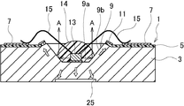
- Example 1 It is principal part sectional drawing which mounted LED on the metal base circuit board.
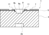
- Example 1 It is principal part sectional drawing of a metal base circuit board.
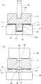
- Example 1 (A) is sectional drawing which shows a convex part formation process and a peeling process, (b) is sectional drawing which shows a mounting part formation process.
- Example 1 It is sectional drawing which shows the height adjustment of an electronic component mounting part.
- Example 1 It is sectional drawing which shows peeling of an insulating layer and copper foil.
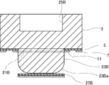
- Example 1 It is sectional drawing which shows peeling of an insulating layer and copper foil.
- Example 1 It is principal part sectional drawing of a metal base circuit board. (Example 2)
- the purpose is to attach electronic parts directly to a metal base to improve heat dissipation and enable high-density mounting, while being able to process at low cost and to suppress scratches, etc. This was realized by punching the insulating layer by half punching of a metal-based convex portion provided with a metal foil and pressing the convex portion.
- FIG. 1 is a plan view of a main part in which an LED is mounted on a metal base circuit board
- FIG. 2 is a cross-sectional view of the main part in which the LED is mounted on a metal base circuit board
- FIG. 3 is a cross-sectional view of the main part of the metal base circuit board. is there.
- the metal base circuit board 1 is manufactured by a manufacturing method described later.
- a metal foil for a circuit is provided on one side surface of a metal base 3 made of aluminum or aluminum alloy with an insulating layer 5 interposed therebetween.
- a copper foil pattern 7 is provided.
- the metal base 3 includes an electronic component mounting portion 9 without the insulating layer 5 and the copper foil pattern 7.
- the electronic component mounting portion 9 has a flat bottom mounting surface 9a and an inclined side wall portion 9b, and has a concave cross section.
- a discarded copper foil 11 is formed in a circular shape around the electronic component mounting portion 9. This discarded copper foil 11 is left to facilitate the punching of the insulating layer 5 and does not constitute a circuit. However, the discarded copper foil 11 can also be used as a ground circuit or the like.
- an LED 13 is attached as an electronic component to the central portion of the mounting surface 9a with a conductive paste (silver powder + epoxy resin) or the like.
- the LED 13 is connected to the copper foil pattern 7 for a circuit by a metal wire 15 formed by wire bonding or the like.
- the LED 13 is directly attached to the electronic component mounting portion 9 so that the heat generated by the LED 13 can be directly and efficiently transferred to the electronic component mounting portion 9.
- the LED 13 can be protected by being disposed inside the concave electronic component mounting portion 9, and the protrusion onto the metal base 3 can also be restricted.
- FIG. 4A shows a convex portion forming step and a peeling step
- FIG. 4B is a cross-sectional view showing a mounting portion forming step.
- an electron without the insulating layer 5 and the copper foil pattern 7 is provided on one side of the metal base 3 provided with the copper foil pattern 7 for a circuit through the insulating layer 5.
- the component mounting portion 9 is formed, and includes a convex portion forming step S1, a peeling step S2, and a mounting portion forming step S3.
- a copper foil pattern 7 for a circuit is provided through the insulating layer 5 on the entire surface before half-cutting, and as a metal foil to be punched, A dummy copper foil pattern 21 for assisting the punching of the insulating layer 5 is provided in a circular shape.
- the insulating layer 5 and the copper foil patterns 7 and 21 are formed as follows, for example. That is, the metal base 3 is disposed on one surface of the semi-cured insulating material, the copper foil is disposed on the other surface, integrated by a laminating press to form a copper-clad laminated structure, and this copper foil surface is etched Copper foil patterns 7 and 21 are formed.
- a round bar-shaped punch 16 and a die 19 provided with a hole 17 are used.
- the clearance between the punch 16 and the hole 17 is set to 2.5% or less, for example. However, this clearance can be set to other settings.
- the metal base 3 is first placed and fixed on the die 19. At this time, the dummy copper foil pattern 21 is positioned so that the center of the dummy copper foil pattern 21 is the center of the hole 17 of the die 19.
- the punch 16 is driven from the other side surface of the metal base 3 to the middle in the thickness direction, and the meat of the metal base 3 is pushed into the hole 17 of the die 19.
- a convex portion 23 is formed in the hole 17 of the die 19 by half punching, and a driven concave portion 25 is formed on the other side surface of the metal base 3. Due to the half-cut formation of the convex portion 23, the insulating layer 5 and a part of the dummy copper foil pattern 21 are punched out at a place where the dummy copper foil pattern 21 is present.
- the dummy copper foil pattern 21 discards the copper foil 11 around the convex portion 23, assists partial punching of the insulating layer 5, and facilitates driving.
- the pushing amount of the punch 16 is about half of the thickness of the metal base 3 in this embodiment. However, the pushing amount can be set to other values.
- the peeling step S2 is performed by setting the clearance between the punch 16 and the hole 17 and setting the pressing amount of the punch 16, and pulls up the metal base 3 after punching from the die 19 so that the convex portion 23 is formed in the hole of the die 19. It is executed by pulling out 17.
- the protrusion 23 is pushed by the punch 16 so that the cross-section of the tip peripheral edge 23 a changes to a curved shape, and the peripheral edge of the punched residue 27 is peeled off from the front peripheral edge 23 a of the convex 23.
- the removed dregs 27 that has been peeled off can be sucked by a suction device or the like connected to the hole 17 of the die 19.
- the cut residue 27, which is a part of the insulating layer 5 and the copper foil pattern 21, is peeled and removed using the peripheral edge portion 23a of the convex portion 23 to expose the tip of the convex portion 23.
- a flat plate punch 29 and a die 33 provided with a cone portion 31 are used.
- the convex part 23 of the metal base 3 whose tip is exposed through the convex part forming step S1 and the peeling step S2 in FIG. 4A is press-molded by the punch 29 and the die 33 as shown in FIG.
- the electronic component mounting portion 9 having a concave cross section without the insulating layer 5 and the copper foil patterns 7 and 21 is formed.
- FIG. 5 is a cross-sectional view showing the height adjustment of the electronic component mounting portion.
- the 2 can be adjusted by a punch 29 and a die 35 as shown in FIG. 5 in the mounting portion forming step S3. That is, the die 35 is formed with an adjustment projection 37 that enters the driving recess 25 formed in the metal base 3, and the balance of the two-way meat movement is adjusted by setting the height of the adjustment projection 37. Can do.
- the degree of the cross-sectional curved shape of the tip peripheral edge portion 23a of the convex portion 23 can be adjusted by selecting the diameter of the punch 16 and the diameter of the hole 17 of the die 19 and the pressing amount of the punch.
- 6 and 7 are cross-sectional views showing the separation of the insulating layer and the copper foil.
- the concave portion 25A is formed by a punch having a small diameter
- the tip of the convex portion 23A is made hemispherical
- the tip peripheral portion 23Aa is formed.
- the insulating layer 5 and the cut residue 27A of the copper foil pattern 21A are completely peeled off simply by forming the convex portion 23A.
- the recessed portion 25B is formed by a punch having a large diameter, and a corner radius is provided in the cross section of the tip peripheral edge portion 23Ba of the convex portion 23B, and the convex portion 23B is formed in a flat base shape.
- the trapezoidal convex portion 23B only the peripheral edge portion of the insulating layer 5 and the punched residue 27B of the copper foil pattern 21B is peeled off.
- the insulating layer 5 and a part of the dummy copper foil pattern 21 can be punched out at a place where the dummy copper foil pattern 21 is present.
- the punched residue 27 which is a part of the insulating layer 5 and the dummy copper foil pattern 21 can be easily peeled and removed using the curved shape of the cross section of the tip peripheral edge portion 23a of the convex portion 23.
- the electronic component mounting portion 9 that enables the LED 13 to be directly attached to the metal base 3 can be easily formed by pressing.
- the electronic component mounting portion 9 is formed by driving and pressing, machining and laser processing are not required, and the electronic component mounting portion 9 can be processed at low cost, and the occurrence of scratches on the electronic component mounting portion 9 is suppressed. be able to.
- the heat generated by the LED 13 can be directly transferred to the electronic component mounting portion 9, heat dissipation can be improved, and high-density mounting can be advanced.
- the metal base 3 was provided with a dummy copper foil pattern 21 for assisting the punching of the insulating layer 5.
- the discarded copper foil 11 can be formed to assist the punching of the insulating layer 5 and can be easily performed.
- the tip of the convex portion 23 is formed into a semispherical shape or a cross section of the tip peripheral portion 23Ba by selecting the diameter of the punch 16 and the diameter of the hole 17 of the die 19 and the pressing amount of the punch 16. It is formed into a trapezoid with a rounded shape.
- the electronic component mounting portion 9 was formed in a concave shape.
- the LED 13 can be protected by being disposed inside the concave electronic component mounting portion 9, and the protrusion onto the metal base 3 can also be restricted.
- the electronic component mounting portion 9 is composed of a flat bottom mounting surface 9a and an inclined side wall portion 9b.
- the connection between the LED 13 mounted on the mounting surface 9a and the copper foil pattern 7 on one side by the wire 15 is connected to the side wall portion 9b. It can be easily performed using the inclination.
- the electronic component mounting part 9 is formed in a concave shape, the light emitted from the LED 13 can be reflected to the front as indicated by the arrow A by the inclined side wall part 9b, and an increase in illuminance can be expected.
- the electronic component mounting portion 9 was formed in a concave shape while returning the meat on the convex portion 23 side into the driving concave portion 25 formed by driving the punch 16 on the other side surface.
- the depth of the electronic component mounting portion 9 can be set freely.
- FIG. 8 is a cross-sectional view of the main part of the metal base circuit board according to the second embodiment.
- the convex portion forming step S1, the peeling step S2, and the mounting portion forming step S3 are the same as in the first embodiment.
- the electronic component mounting portion 9C is flattened. Formed into a shape.
- the flat mounting surface 9Ca of the electronic component mounting portion 9C is integrated with the discarded copper foil 11 and is set at the same height as the upper surface of the copper foil pattern 7.
- the peripheral edge 5a of the insulating layer 5 is deformed toward the other side surface and bites into the meat of the metal base 3C.
- the electronic component mounting portion 9C is flattened while the meat on the convex portion 23 (see FIG. 4) side is returned into the driving recess 25C formed by driving the punch 16 on the other side surface of the metal base 3C.
- the setting of the meat return amount can be performed as shown in FIG.
- the flat mounting surface 9Ca of the electronic component mounting portion 9C By the flat mounting surface 9Ca of the electronic component mounting portion 9C, a highly exothermic semiconductor, for example, a bare chip such as a power switching element, can be directly attached to the metal base 3C in a wide range and efficiently radiated.
- a highly exothermic semiconductor for example, a bare chip such as a power switching element
- the insulating layer 5, the copper foil pattern 7, the dummy copper foil pattern 21, the discarded copper foil 11, and the electronic component mounting portion 9 can be provided on both surfaces of the metal base 3.
- a method of punching out a part of the insulating layer 5 at a place where the copper foil pattern 21 is present may be employed.
- the removal of the removal pieces 27, 27 ⁇ / b> A, 27 ⁇ / b> B, etc. can also be performed after the projections 23, etc. are pulled out from the holes 17 of the die 19.
Landscapes
- Engineering & Computer Science (AREA)
- Microelectronics & Electronic Packaging (AREA)
- Manufacturing & Machinery (AREA)
- Insulated Metal Substrates For Printed Circuits (AREA)
- Led Device Packages (AREA)
Abstract
Description
図1は、金属ベース回路基板にLEDを実装した要部平面図、図2は、金属ベース回路基板にLEDを実装した要部断面図、図3は、金属ベース回路基板の要部断面図である。
[金属ベース回路基板の製造方法]
図4(a)は、凸部形成工程及び剥離工程を示し、(b)は、搭載部形成工程を示す断面図である。
[実施例1の効果]
本発明実施例1では、絶縁層5を介して回路用の銅箔パターン7を備えた金属ベース3の一側面に、前記絶縁層5及び銅箔パターン7の無い電子部品搭載部9を形成する金属ベース回路基板1の製造方法であって、前記金属ベース3の他側面から肉厚方向の途中までパンチ16を打ち込み該金属ベース3の一側面にダイ19の穴17内へ押し込まれ先端周縁部23aの断面が湾曲形状の凸部23を半抜き形成して前記ダミーの銅箔パターン21の有る箇所で絶縁層5及びダミーの銅箔パターン21の一部を打ち抜く凸部形成工程S1と、前記打ち抜けかれた絶縁層5及びダミーの銅箔パターン21の一部である抜きカス27を前記凸部23の湾曲形状を利用して剥離除去し凸部23先端を露出させる剥離工程S2と、前記凸部23をプレス成型して前記電子部品搭載部9を形成する搭載部形成工程S3とを備えた。
[その他]
上記各実施例において、絶縁層5、銅箔パターン7、ダミーの銅箔パターン21、捨て銅箔11及び電子部品搭載部9は、金属ベース3の両面に設けることもできる。
3,3C 金属ベース
5 絶縁層
7 回路用の銅箔パターン(金属箔)
9,9C 電子部品搭載部
11 捨て銅箔
13 LED(電子部品)
17 ダイの穴
19 ダイ
21 ダミーの銅箔パターン
23,23A,23B 凸部
25,25C 打ち込み凹部
27,27A,27B 抜きカス(絶縁層及び金属箔の一部)
Claims (6)
- 絶縁層を介して回路用の金属箔を備えた金属ベースの一側面に、前記絶縁層及び金属箔の無い電子部品搭載部を形成する金属ベース回路基板の製造方法であって、
前記金属ベースの他側面から肉厚方向の途中までパンチを打ち込み該金属ベースの一側面にダイの穴内へ押し込まれ少なくとも先端周縁部の断面が湾曲形状の凸部を半抜き形成して前記絶縁層を打ち抜く凸部形成工程と、
前記打ち抜かれた絶縁層を前記凸部の湾曲形状を利用して剥離除去し凸部先端を露出させる剥離工程と、
前記凸部をプレス成型して前記電子部品搭載部を形成する搭載部形成工程と、
を備えたことを特徴とする金属ベース回路基板の製造方法。 - 請求項1記載の金属ベース回路基板の製造方法であって、
前記金属ベースは、前記絶縁層の打ち抜きを補助するダミーの金属箔を有する、
ことを特徴とする金属ベース回路基板の製造方法。 - 請求項1又は2記載の金属ベース回路基板の製造方法であって、
前記凸部形成工程は、前記パンチの径及びダイの穴の径の選択及びパンチの押し込み量の選択により前記凸部の先端を半球状又は先端周縁部の断面にコーナーアールを備えた台状に形成する、
ことを特徴とする金属ベース回路基板の製造方法。 - 請求項1~3のいずれかに記載の金属ベース回路基板の製造方法であって、
前記搭載部形成工程は、前記電子部品搭載部を凹状又は平坦状に形成した、
ことを特徴とする金属ベース回路基板の製造方法。 - 請求項1~4のずれかに記載の金属ベース回路基板の製造方法であって、
前記搭載部形成工程は、前記他側面に前記パンチの打ち込みにより形成された打ち込み凹部内に前記凸部側の肉を戻しつつ電子部品搭載部を凹状又は平坦状に形成した、
ことを特徴とする金属ベース回路基板の製造方法。 - 請求項1~5のいずれかに記載の金属ベース回路基板の製造方法により製造される金属ベース回路基板であって、
前記絶縁層を介して回路用の金属箔を備えた金属ベースの一側面に、前記絶縁層及び金属箔の無い電子部品搭載部を備えた、
ことを特徴とする金属ベース回路基板。
Priority Applications (2)
| Application Number | Priority Date | Filing Date | Title |
|---|---|---|---|
| CN201180006953.3A CN102714924B (zh) | 2010-01-27 | 2011-01-13 | 金属底座电路基板的制造方法以及金属底座电路基板 |
| KR1020127016989A KR101373119B1 (ko) | 2010-01-27 | 2011-01-13 | 금속베이스회로기판의 제조방법 및 금속베이스회로기판 |
Applications Claiming Priority (2)
| Application Number | Priority Date | Filing Date | Title |
|---|---|---|---|
| JP2010016005A JP5430422B2 (ja) | 2010-01-27 | 2010-01-27 | 金属ベース回路基板の製造方法及び金属ベース回路基板 |
| JP2010-016005 | 2010-01-27 |
Publications (1)
| Publication Number | Publication Date |
|---|---|
| WO2011093019A1 true WO2011093019A1 (ja) | 2011-08-04 |
Family
ID=44319018
Family Applications (1)
| Application Number | Title | Priority Date | Filing Date |
|---|---|---|---|
| PCT/JP2011/000157 Ceased WO2011093019A1 (ja) | 2010-01-27 | 2011-01-13 | 金属ベース回路基板の製造方法及び金属ベース回路基板 |
Country Status (4)
| Country | Link |
|---|---|
| JP (1) | JP5430422B2 (ja) |
| KR (1) | KR101373119B1 (ja) |
| CN (1) | CN102714924B (ja) |
| WO (1) | WO2011093019A1 (ja) |
Families Citing this family (1)
| Publication number | Priority date | Publication date | Assignee | Title |
|---|---|---|---|---|
| DE102019118966A1 (de) * | 2019-07-12 | 2021-01-14 | Automotive Lighting Reutlingen Gmbh | Verfahren zum Herstellen einer Schaltungsträgerplatte und Schaltungsträgerplatte |
Citations (5)
| Publication number | Priority date | Publication date | Assignee | Title |
|---|---|---|---|---|
| US5220487A (en) * | 1992-01-27 | 1993-06-15 | International Business Machines Corporation | Electronic package with enhanced heat sinking |
| JPH11284092A (ja) * | 1998-03-27 | 1999-10-15 | Mitsui High Tec Inc | 半導体装置 |
| JP2002094112A (ja) * | 2001-08-10 | 2002-03-29 | Toyoda Gosei Co Ltd | 3族窒化物化合物半導体発光素子の製造方法 |
| WO2004027866A2 (fr) * | 2002-09-23 | 2004-04-01 | Johnson Controls Technology Company | Procede d'etablissement d'une liaison dans un substrat metallique integre |
| JP2006080141A (ja) * | 2004-09-07 | 2006-03-23 | Stanley Electric Co Ltd | 発光装置、その発光装置に使用するリードフレーム、及びリードフレームの製造方法 |
Family Cites Families (1)
| Publication number | Priority date | Publication date | Assignee | Title |
|---|---|---|---|---|
| CN2713647Y (zh) * | 2004-07-27 | 2005-07-27 | 葛世潮 | 功率型白光发光二极管 |
-
2010
- 2010-01-27 JP JP2010016005A patent/JP5430422B2/ja active Active
-
2011
- 2011-01-13 CN CN201180006953.3A patent/CN102714924B/zh active Active
- 2011-01-13 WO PCT/JP2011/000157 patent/WO2011093019A1/ja not_active Ceased
- 2011-01-13 KR KR1020127016989A patent/KR101373119B1/ko active Active
Patent Citations (5)
| Publication number | Priority date | Publication date | Assignee | Title |
|---|---|---|---|---|
| US5220487A (en) * | 1992-01-27 | 1993-06-15 | International Business Machines Corporation | Electronic package with enhanced heat sinking |
| JPH11284092A (ja) * | 1998-03-27 | 1999-10-15 | Mitsui High Tec Inc | 半導体装置 |
| JP2002094112A (ja) * | 2001-08-10 | 2002-03-29 | Toyoda Gosei Co Ltd | 3族窒化物化合物半導体発光素子の製造方法 |
| WO2004027866A2 (fr) * | 2002-09-23 | 2004-04-01 | Johnson Controls Technology Company | Procede d'etablissement d'une liaison dans un substrat metallique integre |
| JP2006080141A (ja) * | 2004-09-07 | 2006-03-23 | Stanley Electric Co Ltd | 発光装置、その発光装置に使用するリードフレーム、及びリードフレームの製造方法 |
Also Published As
| Publication number | Publication date |
|---|---|
| KR101373119B1 (ko) | 2014-03-12 |
| KR20120092685A (ko) | 2012-08-21 |
| CN102714924A (zh) | 2012-10-03 |
| JP5430422B2 (ja) | 2014-02-26 |
| CN102714924B (zh) | 2015-03-11 |
| JP2011155153A (ja) | 2011-08-11 |
Similar Documents
| Publication | Publication Date | Title |
|---|---|---|
| JP2011139008A (ja) | 熱と電気の伝導経路を分離させたチップオンボード用金属基板構造 | |
| JP4329678B2 (ja) | 半導体装置に用いるリードフレームの製造方法 | |
| US6864567B2 (en) | Base of LED | |
| CN107331659A (zh) | Led电路板、终端设备及led电路板的制作方法 | |
| CN105578753A (zh) | 软硬结合板及其制备方法 | |
| CN1677665A (zh) | 电路装置及其制造方法 | |
| JP5430422B2 (ja) | 金属ベース回路基板の製造方法及び金属ベース回路基板 | |
| JP2006294701A (ja) | 半導体装置及びその製造方法 | |
| JP2011018699A (ja) | 電子回路ユニットおよびその製造方法 | |
| US9521756B2 (en) | Power module package and method of fabricating the same | |
| JP4631785B2 (ja) | 金属ベース回路板及びその製造方法、実装部品、モジュール | |
| JP5178648B2 (ja) | パッケージの製造方法、及び半導体装置 | |
| JP2012182207A (ja) | Led素子用リードフレームおよびその製造方法 | |
| JP2012104542A (ja) | Led発光素子用リードフレーム及びそれを用いたledパッケージ、およびその製造方法 | |
| JP4935320B2 (ja) | 部品内蔵多層配線基板装置及びその製造方法 | |
| JP2010087442A (ja) | 半導体装置及びその製造方法 | |
| CN205452352U (zh) | 易散热led支架 | |
| JP4719630B2 (ja) | 転写基板の製造方法 | |
| JP2009267061A (ja) | 配線基板の製造方法 | |
| JP2012182210A (ja) | Led素子用リードフレーム基板の製造方法 | |
| JP4311294B2 (ja) | 電子装置およびその製造方法 | |
| JP3889710B2 (ja) | 混成集積回路装置 | |
| JP2012182209A (ja) | Led素子用リードフレーム基板の製造方法 | |
| CN105026144A (zh) | 结构体和无线通信装置 | |
| JP5779876B2 (ja) | 素子搭載基板の製造方法 |
Legal Events
| Date | Code | Title | Description |
|---|---|---|---|
| WWE | Wipo information: entry into national phase |
Ref document number: 201180006953.3 Country of ref document: CN |
|
| 121 | Ep: the epo has been informed by wipo that ep was designated in this application |
Ref document number: 11736736 Country of ref document: EP Kind code of ref document: A1 |
|
| ENP | Entry into the national phase |
Ref document number: 20127016989 Country of ref document: KR Kind code of ref document: A |
|
| NENP | Non-entry into the national phase |
Ref country code: DE |
|
| 122 | Ep: pct application non-entry in european phase |
Ref document number: 11736736 Country of ref document: EP Kind code of ref document: A1 |